

Page 1

CIO-DAC04/12-HS
User’s Manual
Revision 2
October, 2000
Page 2

LIFETIME WARRANTY
Every hardware product manufactured by Measurement Computing Corp. is warranted against defects in materials or workmanship for
the life of the product, to the original purchaser. Any products found to be defective will be repaired or replaced promptly.
LIFETIME HARSH ENVIRONMENT WARRANTY
TM
Any Measurement Computing Corp. product which is damaged due to misuse may be replaced for only 50% of the current price. I/O
boards face some harsh environments, some harsher than the boards are designed to withstand. When that happens, just return the
board with an order for its replacement at only 50% of the list price. Measurement Computing Corp. does not need to profit from your
misfortune. By the way, we will honor this warranty for any other manufacture’s board that we have a replacement for!
30 DAY MONEY-BACK GUARANTEE
Any Measurement Computing Corp. product may be returned within 30 days of purchase for a full refund of the price paid for the
product being returned. If you are not satisfied, or chose the wrong product by mistake, you do not have to keep it. Please call for a
RMA number first. No credits or returns accepted without a copy of the original invoice. Some software products are subject to a
repackaging fee.
These warranties are in lieu of all other warranties, expressed or implied, including any implied warranty of merchantability or fitness for a particular application. The remedies provided herein are the buyer’s sole and exclusive remedies. Neither Measurement
Computing Corp., nor its employees shall be liable for any direct or indirect, special, incidental or consequential damage arising
from the use of its products, even if Measurement Computing Corp. has been notified in advance of the possibility of such damages.
MEGA-FIFO, the CIO prefix to data acquisition board model numbers, the PCM prefix to data acquisition board model numbers,
PCM-DAS08, PCM-D24C3, PCM-DAC02, PCM-COM422, PCM-COM485, PCM-DMM, PCM-DAS16D/12, PCM-DAS16S/12,
PCM-DAS16D/16, PCM-DAS16S/16, PCI-DAS6402/16, Universal Library, InstaCal, Harsh Environment Warranty and Measure-
ment Computing Corp. are registered trademarks of Measurement Computing Corp.
IBM, PC, and PC/AT are trademarks of International Business Machines Corp. Windows is a trademark of Microsoft Corp. All other
trademarks are the property of their respective owners.
Information furnished by Measurement Computing Corp. is believed to be accurate and reliable. However, no responsibility is
assumed by Measurement Computing Corp. neither for its use; nor for any infringements of patents or other rights of third parties,
which may result from its use. No license is granted by implication or otherwise under any patent or copyrights of Measurement Computing Corp.
All rights reserved. No part of this publication may be reproduced, stored in a retrieval system, or transmitted, in any form by any
means, electronic, mechanical, by photocopying, recording or otherwise without the prior written permission of Measurement Comput-
ing Corp.
Notice
Measurement Computing Corp. does not authorize any Measurement Computing Corp. product for use in life support systems and/or devices without the written approval of the President of Measurement Computing Corp. Life
support devices/systems are devices or systems which, a) are intended for surgical implantation into the body, or
b) support or sustain life and whose failure to perform can be reasonably expected to result in injury. Measurement Computing Corp. products are not designed with the components required, and are not subject to the testing required to ensure a level of reliability suitable for the treatment and diagnosis of people.
HM CIO-DAC04_12-HS.lwp
Page 3

1. INTRODUCTION
2. INSTALLATION
2.1 SOFTWARE INSTALLATION
2.2 BASE ADDRESS SELECTION
2.3 OUTPUT RANGE SELECTION
3. CONNECTIONS
3.1 MAIN CONNECTOR DIAGRAM
3.2 ANALOG OUTPUTS
4. PROGRAMMING
.................................................................................
.....................................................................................
......................................................................
....................................................................
....................................................................
.....................................................................................
..................................................................
..............................................................................
...................................................................................
4.1 CUSTOM SOFTWARE UTILIZING THE UNIVERSAL LIBRARY
4.2 FULLY INTEGRATED SOFTWARE PACKAGES (e.g., HP VEE)
4.3 DIRECT REGISTER LEVEL PROGRAMMING
5. CALIBRATION AND TEST
5.1 REQUIRED EQUIPMENT
.........................................................................
........................................................................
5.2 CALIBRATING THE D/A CONVERTERS
6. SPECIFICATIONS
..................................................................................
.....................................................
..........................................................
....................................
...................................
1
1
1
1
2
3
3
3
5
5
5
5
8
8
9
10
i
Page 4

This page is blank.
ii
Page 5

1. INTRODUCTION
The installation and operation of the CIO-DAC04/12-HS board is very simple. Use InstaCalTM to help you quickly and easily setup,
install and test your board. We assume you already know how to open the PC and install expansio n boards. If you are unfamiliar or
uncomfortable with board installation, please refer to your computer’s documentation.
2. INSTALLATION
2.1 SOFTWARE INSTALLATION
The CIO-DAC04/12-HS has a variety of switches to set before installing the board in your computer. By far the simplest way to
configure your bo ard is to use InstaCal. It will show you all available options, how to configure the various switches and j umpers to
match your application requirements, and will create a configuration file that your application software (and the Universal Library) will
refer to so the software you use will automatically know the exact configuration of the board. Refer to the Software Installation
Manual to install InstaCal.
Details regarding the setting of the switches are shown below.
2.2 BASE ADDRESS SELECTION
Unless there is already a board in your system using address 300h (768 decimal), we recommend you leave the switches as they are set
at the factory. The location of the Base Address switches is shown on Figure 2-2.
In Figure 2-1 below, the base address is shown set to 300h.
Figure 2-1. Base Address Switches Set to 300h
NOTE: The Base Address switches are additive and ON (active) when DOWN, and OFF when UP.
-1-
Page 6

2.3 OUTPUT RANGE SELECTION
The analog output full-scale ranges are set by DIP switches. Each analog channel has a separate set of switches. The location of the
switches and the channels they control are shown in the Figures 2-2.
CIO-DAC04/12-HS
Table 2-1 CIO-DAC04/12-HS Range Switch Settings
NOTE: UP = ON, DOWN = OFF
Figure 2-2. CIO-DAC04/12-HS Switch Locations
S4S3S2S1OUTPUT FULL - SCALE RANGE
OFFOFFONON+/-10V
ONOFFONON+/-5V
OFFONONON+/-2.5V
OFFOFFOFFOFF0 to 10V
ONOFFOFFOFF0 to 5V
OFFONOFFOFF0 to 2.5V
-2-
Page 7

3. CONNECTIONS
3.1 MAIN CONNECTOR DIAGRAM
All user-connections to the CIO-DAC04/12-HS are made thro ugh a 37 pin “D” connector accessib le from the rear of the P C (through
the expansion back plate).
The connector accepts female 37 D-type connectors, such as those on the C37FF-2 (a two foot cable). If frequent changes to signal
connections or signal conditioning is required we strongly recommend purchasing the CIO-MINI37 screw terminal board with the
mating C37FF-2 cable.
CIO-DAC04/12-HS SIGNAL CONNECTOR
Figure 3-1. I/O Connector Pinout
-3-
Page 8
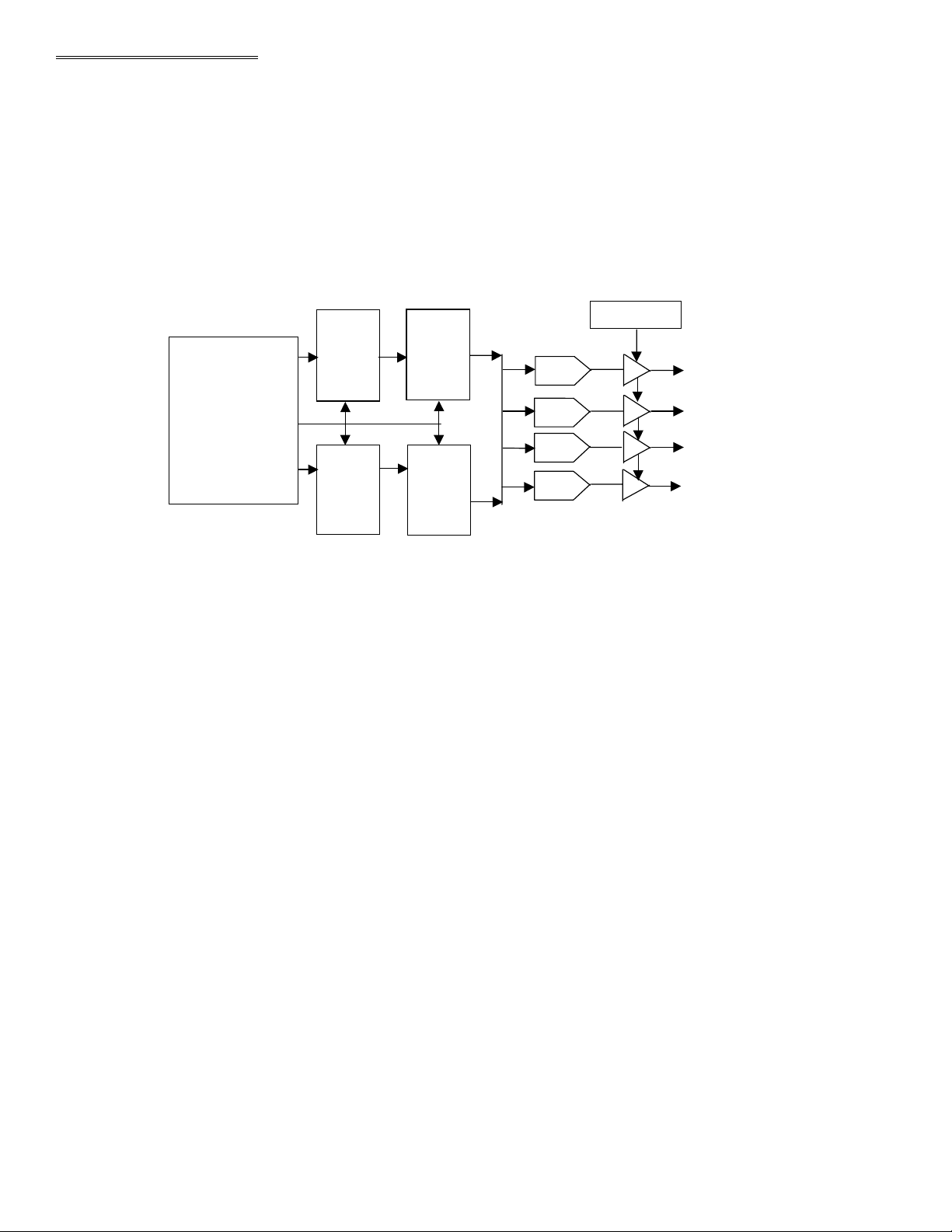
3.2 ANALOG OUTPUTS
Analog outputs are voltage outputs which can be connected to any device which will record, display or be contro lled by a vo ltage. The
CIO-DAC04/12-HS analog outputs are produced with four quadrant-multiplying DACs. They accept an input voltage reference and
provide an output voltage which is inverse to the reference voltage and proportional to the digital value in the output register.
For example, in unipolar mode, the supplied reference of −5V provides a +5V output when the value in the output register is 4095 (full
scale at 12-bits of resolution). It provides a value of 2.5V when the value in the output register is 2048.
Figure 3-2 is a simplified block diagram of the CIO-DAC04/12-HS.
DAC Control
DIO Control
Decoder Logic
FIFO
Upper
Byte
FIFO
Lower
Byte
DAC
Upper
Byte
Control
DAC
Lower
Byte
Control
Figure 3-2. D/A Output Configuration
Gain Select
DA
DA
T
2
T
-4-
Page 9

4. PROGRAMMING
There are three common approaches to programming the CIO-DAC04/12-HS board. They are:
y
Writing custom software utilizing our Universal Library package,
y
Using a fully integrated software package (e.g. Labtech Notebook), or
y
Direct register-level programming.
4.1 CUSTOM SOFTWARE UTILIZING THE UNIVERSAL LIBRARY
Most customers write custom software using Universal Library™. The Universal Library takes care of all the board I/O commands and
lets you concentrate on the application part of the software. For additional information regarding using the Universal Library, please
refer to the documentation supplied with the Universal Library.
4.2 FULLY INTEGRATED SOFTWARE PACKAGES (e.g., HP VEE)
Many customers also take advantage of the power and simplicity offered by one of the upper level data acquisition packages. Please
refer to the package’s documentation for setup and usage details.
4.3 DIRECT REGISTER LEVEL PROGRAMMING
Though uncommon, some applica tions do not allow the use of our Universal Lib rary, and are not a good match for an upper level
package. For experienced programmers we provide detailed register mapping below.
InstaCal is a complete installation, calibration and test package. Use it to guide the installation proced ure and to calibrate your data
acquisition board. InstaCal also creates a configuration file required for programmers who use the Universal Library programming
libraries.
REGISTER LEVEL PROGRAMMING INFORMATION
We recommend that users make use of our Universal Library programming interface. The following section is provided for those
experienced programmers who do not wish to take advantage of the control programs already built into the Universal Library.
Single Output:
1.
Clear the START bit.
2.
Select channel.
3.
Disable and reset interrupts.
4.
Clear FIFO.
5.
Write MSB to Base + 1, then LSB to Base + 0. DAC updates upon writing to Base + 0.
1023 samples or less:
(No interrupt necessary).
1.
Stop pacer by setting 8254 to mode 2.
2.
Clear FIFO.
3.
Disable and reset interrupts.
4.
Set channel limits.
5.
Set START bit to hold off pacer.
6.
Initialize the 8254.
7.
Load FIFO with new data.
-5-
Page 10

8.
Toggle START bit to start pacer.
1024 samples or more:
1.
Stop pacer by setting 8254 to mode 2.
2.
Clear FIFO.
3.
Disable and reset interrupts.
4.
Set channel limits.
5.
Set START bit to hold off pacer.
6.
Initialize the 8254.
7.
Load FIFO with first 1024 samples.
8.
Install Interrupt Service Routine (ISR).
9.
Enable interrupts and clear START bit. The DACs will begin updating immediately.
Upon the FIFO becoming half-empty, the board will assert an INT. The ISR is responsible for filling the FIFO with 256 samples on
each interrupt. Upon filling the FIFO with the last of the data, the ISR should disable the interrupts and be un-installed.
CIO-DAC04/12-HS REGISTER MAP
Base + 0 (DAC LSB)
RD -------------------- RESETS INTERRUPT ------------------------------WR D3 D2 D1 D0 N/A N/A N/A N/A
Base + 1 (DAC MSB)
RD ------------------- RESETS FIFO -----------------------------------------WR D11 D10 D9 D8 D7 D6 D5 D4
Base + 2 (Channel select)
RD N/A N/A H1 H0 N/A N/A L1 L0
WR N/A N/A H1 H0 N/A N/A L1 L0
This address sets the active D/A channels. The channels selected must be consecutive. This register sets a start channel and a stop
channel. Channels in-between are automatically written to. You cannot jump channels between your start and stop channels. (i.e., if
you start at ch 1 and stop at ch 3, you will also write data to ch 2) The table below describes the start/stop channel selections.
gh or Stop Channel Low or Start Channel
Hi
CH H1 H0 CH L1 L0
000 000
101 101
210 210
311 311
The stop channel must always be greater than or equal to the start channel. For single channel operation, Start Ch. = Stop Ch.
Base + 3 (Control / Status)
RD INTE INT2 INT1 INT0 FFE FFHF FFERR INTST
WR INTE INT2 INT1 INT0 N/A N/A SIMUL START
Control Register Description (Write Base + 3):
Bit #
0 START Used when total count is less than 1024. Setting the START bit starts DAC output
Name Description
process. Since count is less than 1024, no interrupts are required.
= 0 Pacer starts when sample #1024 is written.
= 1 Transfers one sample if 8254 not programmed (Direct mode).
-6-
Page 11

1 SIMUL DAC Simultaneous update mode. All DAC's are updated when Channel 3 is updated.
= 0 Normal DAC update mode (as data comes in).
= 1 Simultaneously updates all four DAC's when Channel 3 accessed.
2,3 Not Used
4-6 INT# Selects Interrupts 2-7.
INT2 INT1 INT0 IRQ selected
0 0 0 None
0 0 1 None
0102
0113
1004
1015
1106
1117
7 INTE Interrupt Enable.
= 0 Interrupts disabled (default).
= 1 Interrupts enabled.
Status Register Description (Read Base + 3)
Bit #
Name Description
0 INTST Interrupt flip-flop status. Clocked high when FIFO goes
less than half-full. Requires active pacer gate, does not require Interrupt enable.
(Resets interrupt)
1 FFERR FIFO Error Status. Goes high if FIFO went empty during pacing. Valid only while
pacer clock is active. (Resets FIFO).
2 FFHF FIFO Half Full. Low when FIFO has 512 samples or more.
3 FFE FIFO Empty. Low when FIFO is empty.
4-6 INT# Reads Selected Interrupt.
7 INTE Interrupt Enable
Base + 4 (Digital Input / Output)
RD DIN7 DIN6 DIN5 DIN4 DIN3 DIN2 DIN1 DIN0
WR DOUT7 DOUT6 DOUT5 DOUT4 DOUT3 DOUT2 DOUT1 DOUT0
Base + 5 ----------------------------------------------- NOT USED ---------------------------------------------
Base + 6 ----------------------------------------------- NOT USED ---------------------------------------------
Base + 7 ----------------------------------------------- NOT USED ---------------------------------------------
-7-
Page 12

Base + 8 (Counter 0 Data)
RD D7 D6 D5 D4 D3 D2 D1 D0
WR D7 D6 D5 D4 D3 D2 D1 D0
Base + 9 (Counter 1 Data)
RD D7 D6 D5 D4 D3 D2 D1 D0
WR D7 D6 D5 D4 D3 D2 D1 D0
Base + 10 (Counter 2 Data)
RD D7 D6 D5 D4 D3 D2 D1 D0
WR D7 D6 D5 D4 D3 D2 D1 D0
Base + 11 (Counter Control)
RD ----------------------------------------------- NOT USED --------------------------------------------WR D7 D6 D5 D4 D3 D2 D1 D0
Definitions
DA11:0 "DAC04HS/12 - DAC Data bits: D11 = MSB, D0 = LSB (LEFT-JUSTIFIED)"
CHxH DAC channel selection upper limit
CHxL DAC channel selection lower limit
Examples:
"To sample channel 1: Set CH2L/CH1L to 0/1, CH2H/CH1H to 0/1"
"To sample channels 1 to 2: Set CH2L/CH1L to 0/1 (1), CH2H/CH1H to 1/0 (2)"
"To sample channels 0 to 3: Set CH2L/CH1L to 0/0 (0), CH2H/CH1H to 1/1 (3)"
FFE "FIFO Empty: = 0 when empty, = 1 when not empty"
FFHF "FIFO Half Full: = 0 when > half full, = 1 when < half full (512 samples)"
FFERR FIFO Error: = 1 if FIFO went empty during pacing (valid while pacer active)
INTST Interrupt Status: = 1 when FIFO half full
INTE "Interrupt Enable: = 0 to enable interrupts, = 1 to disable"
SIMUL Simultaneous Update Mode: = 1 to enable simultaneous update of all 4 DAC's
START Start DAC conversions: = 1 to start conversions from pacer controlled
:= 0 to transfer 1 sample non-paced (direct mode)
DIN7:0 Digital Input byte
DOUT7:0 Digital Output byte
D7:0 Counter Data byte
INT2:0 Interrupt Select
-8-
Page 13

5. CALIBRATION AND TEST
Every board was fully tested and calibrated before leaving the factory. For normal environments, a calibration interval of 6 months to
one year is recommended. If frequent variations in temperature or humidity are common, recalibrate at least once every three months.
It requires less than 10 minutes to calibrate the CIO-DAC04/12-HS.
5.1 REQUIRED EQUIPMENT
You will need a 4½ digit digital voltmeter and a few pieces of wire.
You do not need an extender card to calibrate the b oard but you will need to have the cover off your computer with the power on, so
trim pots can be adjusted during calibration. A plastic screwdriver is supplied with your board. In the event that the screwdriver is
dropped into the PC, no damage will result from short circuits.
5.2 CALIBRATING THE D/A CONVERTERS
The D/A's are calibrated by writing a code to the D/A, measuring the analog output voltage and then adjusting potentiometers so that
the output voltage is correct. The entire procedure is described in the Insta
Calibrate each channel for the range you intend to use. When the range is changed, a there may be a slight variation in zero and full
scale gain.
, calibration routine.
Cal
-9-
Page 14

Power Consumption
+5V supply 520 mA typ, 610 mA max.
Analog Output
Resolution 12 bits
Number of channels 4 Voltage Output
D/A type AD7948BN
Voltage Ranges ±2.5, ±5, ±10, 0 to 2.5, 0 to 5, 0 to 10, switch-selectable, each channel independently
D/A Pacing Internal or external clock (EXTPACER) on falling edge or software-paced
D/A Gating External (EXTGATE), active high
Data Transfer Programmed I/O
Offset error Adjustable to zero
Gain error Adjustable to zero
Differential nonlinearity ±0.5 LSB max.
Integral nonlinearity ±0.5 LSB max.
Monotonicity Guaranteed monotonic to 12 bits over temperature
D/A Gain drift 5 ppm FSR/°C max.
Throughput PC-dependent, 250 kHz max.
Settling time (20V step to .01%) 1µs typical, 1.5µs max
Slew rate 32V/µs typical
Current Drive ±5 mA typical
Output short-circuit duration 20 mA min Continuous
Output Coupling DC
Miscellaneous Double buffered output latches
6. SPECIFICATIONS
From 1024 FIFO via programmed I/O or REP-OUTSW interrupt
Update DACs individually or simultaneously (software-selectable)
Simultaneous mode requires that channel 3 is always included in the channels to be
updated.
State of analog outputs at power-up is un-defined.
When using the internal pacer, the user must physically disconnect any signal connected
to the EXTPACER input on the User Connector.
Digital Input / Output
Digital Type Input: 74LS244
Configuration 2 banks of 8, 1 bank as input, 1 bank as output
Number of channels 16
Output High 2.7 volts min @ −0.4 mA
Output Low 0.4 volts max @ 8 mA
Input High 2.0 volts min, 7 volts absolute max
Input Low 0.8 volts max, −0.5 volts absolute min
Power up, reset state of outputs Logic low
Interrupt IRQ 2 - 7, Software-selectable
Interrupt enable Programmable
Interrupt sources D/A FIFO-half-full
Output: 74LS273
-10-
Page 15

Counters Section
Configuration 82C54 device. 3 down-counters, 16 bits each, chained to form a 48-bit counter
Clock input frequency 10 MHz max
High pulse width (clock input) 30 ns min
Low pulse width (clock input) 50 ns min
Gate width high 50 ns min
Gate width low 50 ns min
Input low voltage 0.8V max
Input high voltage 2.0V min
Output low voltage 0.4V max
Output high voltage 3.0V min
Counter 0 - Internal Pacer - First divider
Source: 10 MHz oscillator
Gate: Internal PGATE (FPGA control signal)
Output: Chained to Counter 1 clock input
Counter 1 - Internal Pacer - Second divider
Source: Counter 0 output
Gate: Internal PGATE (FPGA control signal)
Output: Chained to Counter 2 clock input
Counter 2 - Internal Pacer - Third divider
Source: Counter 1 output
Gate: Internal PGATE (FPGA control signal)
Output: Pacer control logic
Environmental
Operating temperature range 0 to 70°C
Storage temperature range −40 to 100°C
Humidity 0 to 90% non-condensing
-11-
Page 16

For your notes.
-12-
Page 17

EC Declaration of Conformity
We, Measurement Computing Corp., declare under sole responsibility that the product:
ISA Bus, high speed analog output boardCIO-DAC04/12-HS
DescriptionPart Number
to which this declaration relates, meets the essential requirements, is in conformity with, and CE marking has been applied according to the
relevant EC Directives listed below using the relevant section of the following EC standards and other normative documents:
EU EMC Directive 89/336/EEC: Essential requirements relating to electromagnetic compatibility.
EU 55022 Class B: Limits and methods of measurements of radio interference characteristics of information technology equipment.
EN 50082-1: EC generic immunity requirements.
IEC 801-2: Electrostatic discharge requirements for industrial process measurement and control equipment.
IEC 801-3: Radiated electromagnetic field requirements for industrial process measurements and control equipment.
IEC 801-4: Electrically fast transients for industrial process measurement and control equipment.
Carl Haapaoja, Director of Quality Assurance
Page 18

Measurement Computing Corporation
16 Commerce Boulevard,
Middleboro, Massachusetts 02346
(508) 946-5100
Fax: (508) 946-9500
E-mail: info@measurementcomputing.com
www. measurementcomputing.com
 Loading...