

Page 1

ADAC/5500 Series User’s Manual
12-Bit and 16-Bit PCI Data Acquisition Series Boards
the smart approach to instrumentation ™
IOtech, Inc.
25971 Cannon Road
Cleveland, OH 44146-1833
Phone: (440) 439-4091
Fax: (440) 439-4093
E-mail (sales): sales@iotech.com
E-mail (post-sales): productsupport@iotech.com
Internet:
www.iotech.com
ADAC/5500 Series
Data Acquisition Boards
© 2002, 2003, 2004 by IOtech, Inc. 928795 Printed in the United States of America
1107-0905 Rev 2.0
p/n
Page 2
Warranty Information
Your IOtech warranty is as stated on the product warranty card. You may contact IOtech by phone, fax machine, or
e-mail in regard to warranty-related issues. Phone: (440) 439-4091, fax: (440) 439-4093, e-mail: sales@iotech.com
Limitation of Liability
IOtech, Inc. cannot be held liable for any damages resulting from the use or misuse of this product.
Copyright, Trademark, and Licensing Notice
All IOtech documentation, software, and hardware are copyright with all rights reserved. No part of this product may be
copied, reproduced or transmitted by any mechanical, photographic, electronic, or other method without IOtech’s prior written
consent.
other product names, as applicable, are trademarks of their respective holders. All supplied IOtech software (including
miscellaneous support files, drivers, and sample programs) may only be used on one installation. You may make archival
backup copies.
DIRECT CONNECTTM is a Registered Trademark of IOtech, Inc. IOtech product names are trademarked;
CE Notice
Many IOtech products carry the CE marker indicating they comply with the safety and emissions standards of the European
Community. As applicable, we ship these products with a Declaration of Conformity stating which specifications and
operating conditions apply.
Warnings, Cautions, Notes, and Tips
Refer all service to qualified personnel. This caution symbol warns of possible personal injury or equipment damage under
noted conditions. Follow all safety standards of professional practice and the recommendations in this manual. Using this
equipment in ways other than described in this manual can present serious safety hazards or cause equipment damage.
This warning symbol is used in this manual or on the equipment to warn of possible injury or death from electrical shock
under noted conditions.
This ESD caution symbol urges proper handling of equipment or components sensitive to damage from electrostatic
discharge. Proper handling guidelines include the use of grounded anti-static mats and wrist straps, ESD-protective bags and
cartons, and related procedures.
This symbol indicates the message is important, but is not of a Warning or Caution category. These notes can be of great
benefit to the user, and should be read.
In this manual, the book symbol always precedes the words “Reference Note.” This type of note identifies the location of
additional information that may prove helpful. References may be made to other chapters or other documentation.
Tips provide advice that may save time during a procedure, or help to clarify an issue. Tips may include additional reference.
Specifications and Calibration
Specifications are subject to change without notice. Significant changes will be addressed in an addendum or revision to
the manual. As applicable, IOtech calibrates its hardware to published specifications. Periodic hardware calibration is
not covered under the warranty and must be performed by qualified personnel as specified in this manual. Improper
calibration procedures may void the warranty.
Quality Notice
IOtech has maintained ISO 9001 certification since 1996. Prior to shipment, we thoroughly test our products and review
our documentation to assure the highest quality in all aspects. In a spirit of continuous improvement, IOtech welcomes
your suggestions.
1.1
ii
Page 3

Warranty, Warnings, Cautions, and Notes ……………………………………………………....…. iii
1. INTRODUCTION
1.1 CHOICE OF MODELS.......................................................................................................1
1.2 PRODUCT DESCRIPTION ...............................................................................................1
1.2.1 Analog Inputs..............................................................................................................4
1.2.2 Analog Outputs...........................................................................................................4
1.2.3 Digital I/O....................................................................................................................4
1.2.4 Counters 0 and 1 ........................................................................................................4
1.2.5 Timers 0 and 1............................................................................................................4
1.2.6 PCI Interface...............................................................................................................4
1.3 SOFTWARE COMPATIBILITY ..........................................................................................5
1.4 CE COMPLIANCE .............................................................................................................5
1.5 FUSE AND CONNECTOR PLACEMENT..........................................................................6
2. GETTING STARTED
STEP 1 – INSTALL SOFTWARE..................................................................................................7
STEP 2 – INSTALL BOARDS IN AVAILABLE PCI BUS-SLOTS.................................................8
STEP 3 – CONFIGURE BOARDS................................................................................................9
3. HARDWARE CONFIGURATION
3.1 DMA AND INTERRUPT UTILIZATION............................................................................10
3.2 DMA ENGINE ..................................................................................................................11
3.3 ANALOG INPUT CONFIGURATION...............................................................................11
3.4 ADC RANGE....................................................................................................................11
3.5 DAC RANGE....................................................................................................................13
4. EXTERNAL CONNECTIONS
4.1 CONNECTING USER WIRING .......................................................................................14
4.1.1 Signal Types.............................................................................................................14
4.1.2 Choosing A/D Input Configuration............................................................................15
4.1.2.1 Single-Ended.....................................................................................................15
4.1.2.2 Pseudo-Differential (PD)....................................................................................16
4.1.2.3 Fully-Differential (DIFF) .....................................................................................16
4.2 ADAC/5500 SERIES, ON-BOARD CONNECTORS........................................................18
4.2.1 Signal Definitions......................................................................................................18
4.2.1.1 Analog Input Channels......................................................................................19
4.2.1.2 Analog Outputs..................................................................................................19
4.2.1.3 Digital I/O Lines .................................................................................................19
4.2.1.4 Terminal Panel Control......................................................................................19
4.2.1.5 Counters And Timers.........................................................................................20
4.2.1.6 Ground Lines.....................................................................................................21
4.2.1.7 Power Lines.......................................................................................................21
4.2.2 J1 Pin Assignments, ADAC/5500MF Only................................................................22
4.2.3 J1 Pin Assignments, ADAC/5501MF, ADAC/5502MF, ADAC/5503HR, &
ADAC/5504HR..........................................................................................................23
4.2.4 P3 and P5 Pin Assignments.....................................................................................24
4.2.5 Signal Definitions for P3, P5, and G17’s DB37 Connector.......................................25
4.3 SCREW-TERMINAL BOARDS........................................................................................26
4.3.1 ADAC-TB-8 Screw-Terminal Board..........................................................................26
4.3.2 ADAC-TB-16 Screw-Terminal Board........................................................................27
4.3.3 ADAC-DC-37 Screw-Terminal Board .......................................................................28
ADAC Series PCI Boards 938697 -iii- ADAC/5500 Series User Manual
Page 4

5. ADAC/5500 Series PCI CARD OPERATION
5.1 DEVICE DRIVERS...........................................................................................................29
5.1.1 LABVIEW™ ...............................................................................................................29
5.1.2 TESTPOINT™ ...........................................................................................................29
5.1.3 WINDOWS DRIVERS (ADLIB WDM).......................................................................29
5.2 THEORY OF OPERATION..............................................................................................30
5.2.1 Process Definitions ..................................................................................................30
5.2.2 Clocking the ADC......................................................................................................32
5.2.3 Starting (Triggering) an ADC Acquisition..................................................................33
5.2.4 Stopping an ADC Acquisition (Clock).......................................................................34
5.2.5 ADC Clock and FIFO Errors.....................................................................................35
5.2.6 ADC Data Transfer Modes .......................................................................................35
5.2.7 Clocking the DAC......................................................................................................36
5.2.8 Starting (Triggering) a DAC Acquisition....................................................................36
5.2.9 Stopping a DAC Acquisition (CLOCK)......................................................................37
5.2.10 DAC Data Transfer Mode .........................................................................................37
5.2.11 Digital Acquisition......................................................................................................38
6. SPECIFICATIONS
6.1 ADAC/5500MF.................................................................................................................40
6.2 ADAC/5501MF AND ADAC/5502MF...............................................................................43
6.3 ADAC/5503HR AND ADAC/5504HR...............................................................................47
6.4 TERMINATION BOARDS................................................................................................52
6.4.1 ADAC-TB-8...............................................................................................................52
6.4.2 ADAC-TB-16.............................................................................................................53
6.4.3 ADAC-DC-37 ............................................................................................................54
ADAC Series PCI Boards 938697 -iv- ADAC/5500 Series User Manual
Page 5
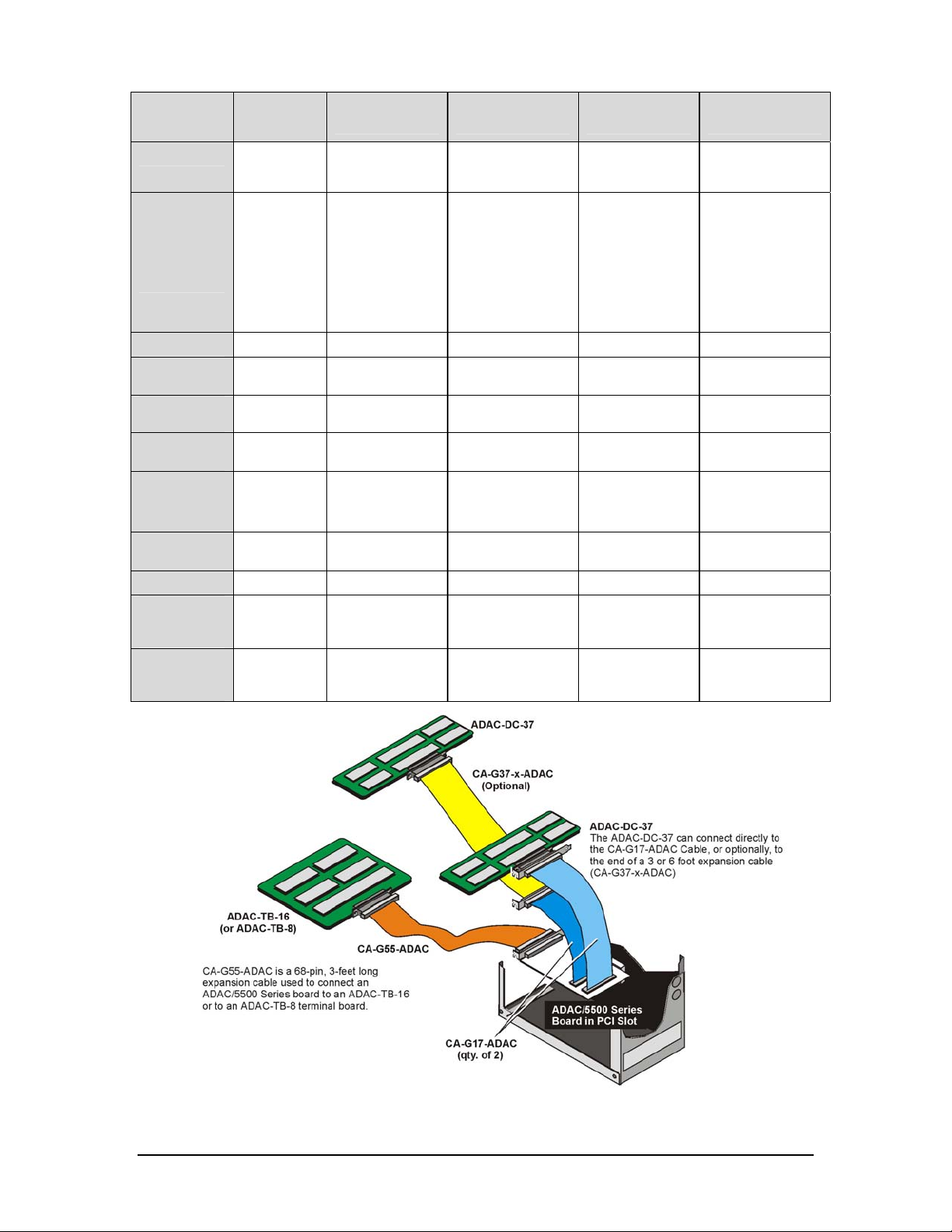
ADAC/5500 Series Boards
Feature
Analog Inputs
Ranges-
Unipolar
Bipolar
Resolution
A/D Sample
Rate
Gains
(Programmable)
D/A Outputs
(16-Bit)
Digital I/O
Counters
(16-Bit)
Timers
Associated
Terminal
Boards
Associated
Cables
(see figure)
/5500MF /5501MF
8 SingleEnded
0 to 10V 0 to10V
± 10V ± 10V
12-bit 12-bit 12-bit 16-bit 16-bit
100 kHz 100 kHz 100 kHz 200 kHz 200 kHz
N/A 1, 2, 4, 8 1, 10, 100, 1000 1, 2, 4, 8 1, 10, 100
0 2 Clocked DACs
16
(Two 8-bit
registers)
2 2 2 2 2
2 2 2 2 2
ADAC-TB-8 ADAC-TB-16
CA-G55ADAC
/5501MF-V
16 Single-Ended, or
16 Pseudo-Diff., or
8 Differential
0 to 5V
0 to 2.5V
0 to 1.25V
± 5V
± 2.5V
± 1.25V
(/5501MF-V only)
16 – from main I/O
(Two 8-bit registers)
16 – from aux. P3*
16 – from aux. P5*
ADAC-DC-37 (qty. 2)
CA-G55-ADAC
CA-G17-ADAC
CA-G37-x-ADAC
/5502MF
/5502MF-V
16 Single-Ended, or
16 Pseudo-Diff., or
8 Differential
0 to10V
0 to 1V
0 to 95mV
0 to 9.5mV
± 10V
± 1V
± 95mV
± 9.5mV
2 Clocked DACs
(/5502MF-V only)
16 – from main I/O
(Two 8-bit registers)
16 – from aux. P3*
16 – from aux. P5*
ADAC-TB-16
ADAC-DC-37 (qty. 2)
CA-G55-ADAC
CA-G17-ADAC
CA-G37-x-ADAC
/5503HR
/5503HR-V
16 Single-Ended, or
16 Pseudo-Diff., or
8 Differential
0 to10V
0 to 5V
0 to 2.5V
0 to 1.25V
± 10V
± 5V
± 2.5V
± 1.25V
2 Clocked DACs
(/5503HR-V only)
16 – from main I/O
(Two 8-bit registers)
16 – from aux. P3*
16 – from aux. P5*
ADAC-TB-16
ADAC-DC-37 (qty. 2)
CA-G55-ADAC
CA-G17-ADAC
CA-G37-x-ADAC
/5504HR
/5504HR-V
16 Single-Ended, or
16 Pseudo-Diff., or
8 Differential
0 to10V
0 to 1V
0 to 99.84 mV
± 10V
± 1V
± 99.86mV
2 Clocked DACs
(/5504HR-V only)
16 – from main I/O
(Two 8-bit registers)
16 – from aux. P3*
16 – from aux. P5*
ADAC-TB-16
ADAC-DC-37 (qty. 2)
CA-G55-ADAC
CA-G17-ADAC
CA-G37-x-ADAC
*
The CA-G17-ADAC cables connect to
40-pin headers P3 (DIO2) and P5 (DIO3)
located on the ADAC Series board.
ADAC/5500 Series, Possible Connections to Terminal Boards
ADAC Series PCI Boards 938697 -v- ADAC/5500 Series User Manual
Page 6

1. INTRODUCTION
1.1 CHOICE OF MODELS
ADAC/5500 PCI Series cards are part of an extensive line of data acquisition boards for use in PCs. ADAC series
boards are low cost and are optimized for use with Windows. We offer “sensor specific” DIRECT CONNECT™
boards, isolated digital I/O boards, boards for DSP applications, and much more. Visit our web site to learn about our
complete line of products.
1.2 PRODUCT DESCRIPTION ADAC/5500 SERIES
The ADAC/5500 Series includes several models of data acquisition boards. These are discussed briefly below, and in
the preceding table. Pages 2 and 3 consist of block diagrams to provide a better understanding of board function.
The ADAC/5500MF has 8 single-ended analog inputs multiplexed to a 12-bit A/D converter with maximum
throughput of 100 kHz, two counter input channels, two timer output channels and 16 lines of digital I/O.
The ADAC/5501MF has 16 single-ended/pseudo-differential or 8 differential analog inputs multiplexed to a 12-bit
A/D converter with maximum throughput of 100 kHz, programmable gains of 1, 2, 4 or 8, two optional clocked 16-bit
D/A voltage outputs, two counter input channels, two timer output channels and 48 lines of digital I/O.
The ADAC/5502MF is the same as the ADAC/5501MF, but with programmable gains of 1, 10, 100 or 1000.
The ADAC/5503HR has 16 single-ended/pseudo-differential or 8 differential analog inputs multiplexed to a 16-bit
A/D converter with maximum throughput of 200 kHz, programmable gains of 1, 2, 4 or 8, two optional clocked 16-bit
D/A voltage outputs, two counter input channels, two timer output channels and 48 lines of digital I/O.
The ADAC/5504HR is the same as the ADAC/5503HR, but with programmable gains of 1, 10, 100.
V-versions of the boards include two clocked DACs, with exception of ADAC/5500MF, which has no “V”- version
counterpart.
All boards feature on-board digital calibration for both A/D and D/A, and a DMA engine for optimum performance in
a Windows environment. Board connections are terminated in a 68-pin “high density” SCSC III connector at the rear of
the PC.
ADAC Series PCI Boards 196 - 1 - ADAC/5500 Series User Manual 908
Page 7
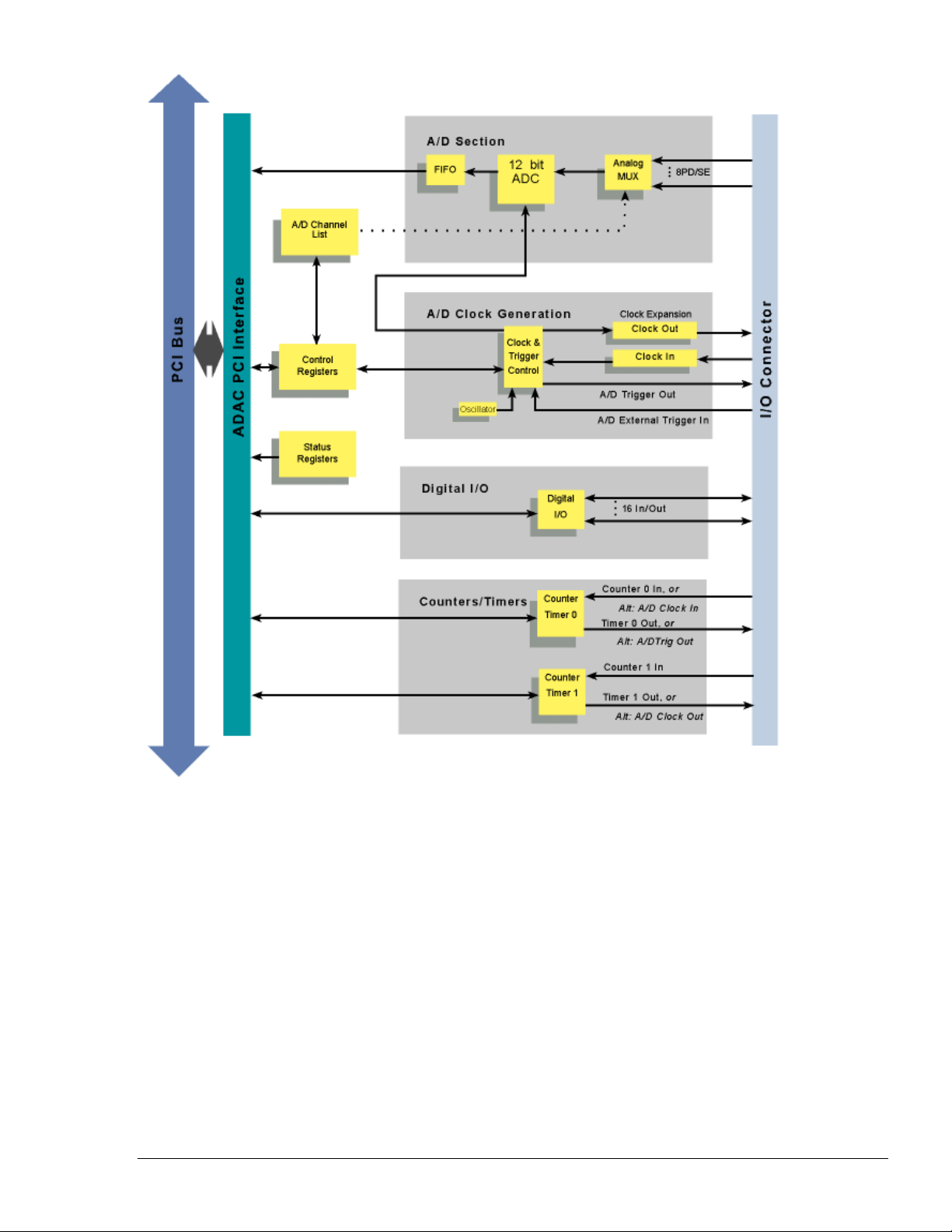
Figure 1.1
Block Diagram for ADAC/5500MF
ADAC Series PCI Boards 196 - 2 - ADAC/5500 Series User Manual
908
Page 8
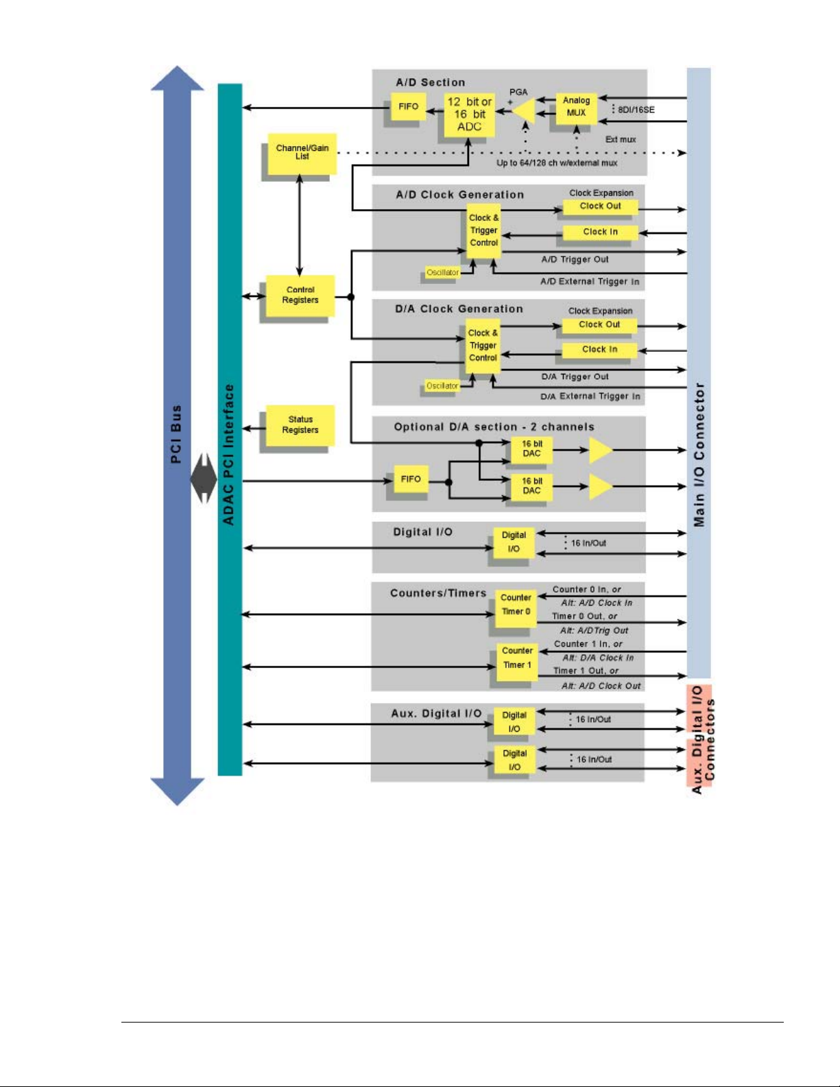
Figure 1.2
Block Diagram for ADAC/5501MF, ADAC/5502MF, ADAC/5503HR and ADAC/5504HR
ADAC Series PCI Boards 196 - 3 - ADAC/5500 Series User Manual
908
Page 9

1.2.1 Analog Inputs
The ADAC/5500MF has 8 single-ended analog inputs multiplexed to a 12-bit A/D converter. The input multiplexer is
supported by 176 elements of channel list RAM, which allows the board to access channels in any order. The 12-bit
A/D has a maximum throughput of 100 kHz and a programmable input range of ±10 V or 0-10 V. An A/D Pacer Clock
is provided to allow sampling rates from 0.0009 Hz to 100 kHz. An on-board Counter/Timer circuit provides two
counters and two timers dedicated to user connections.
The ADAC/5501MF, ADAC/5502MF, ADAC/5503HR and ADAC/5504HR models support 16 single-ended / pseudodifferential analog inputs, or 8 differential analog inputs (expandable to 64) multiplexed to a 12 or 16-bit A/D
converter. The input multiplexer is supported by a 176 element channel gain RAM which allows the board to select
gain on a per channel basis and to access channels in any order. The 12-bit A/D has maximum throughput of 100 kHz
and the 16-bit A/D has a maximum throughput of 200 kHz. An A/D Pacer clock is provided to allow sampling rates
from 0.0009Hz to 200 kHz.
1.2.1.1 4-20mA Current Loop Inputs – n/a
1.2.2 Analog Outputs
The ADAC/5501MF, ADAC/5502MF, ADAC/5503HR and ADAC/5504HR models may be equipped with two
optional clocked DACs (D/A). Both DAC channels are DC accurate with 16-bit resolution and
200 kHz throughput. The output ranges of the DACs are programmable to ±10 V or 0 to +10 V. A Pacer clock is
provided to allow sampling rates from 0.0009Hz to 200 kHz.
1.2.3 Digital I/O
All boards have 16 lines of TTL level digital I/O programmable in 8-bit ports as either inputs or outputs. All 16 lines
are brought out via the main 68-pin SCSI III connector, user accessible at the back of the PC.
Two additional 40 pin headers on the ADAC/550 1MF, ADAC/5502MF, ADAC/5503HR and ADA C/5504HR models
(internal to the PC) provide access to an additional thirty two 5 V CMOS/LSTTL compatible digital lines,
programmable in 16-bit ports as either inputs or outputs. Both sets of digital I/O lines may be brought to the back of the
computer with optional adapter connectors that are compatible with the ADAC line of isolated digital I/O panels.
1.2.4 Counters 0 and 1
Counter 0 and 1 can provide either cumulative or incremental counting capabilities. The counters are capable of
counting 5 V LSTTL rising edges to a maxim um count of 131071 decimal.
1.2.5 Timers 0 and 1
Timer0 and Timer1 provide a 50% duty cycle square wave 5 V LSTTL output with an output frequency range of
7.7 Hz to 500 kHz. The Timer’s output frequency is based on a 1 MHz oscillation with a divisor of 1 to 65536 decimal.
1.2.6 PCI Interface
The ADAC/5500 Series boards communicate to the PCI bus through an ADAC PCI interface controller. The boards are
fully Plug&Play compatible with no switches, potentiometers, or jumpers. The boards feature digitally calibrated A/D
and D/A’s, and Plug&Play compatibility to provide automatic integration into the PC’s configuration when first
installed. The interface also provides access to all on-board registers for software configuration of all on-board
functions. For maximum performance, the ADAC/5500 boards feature a 32-bit bus-mastering DMA engine on the
ADC and DAC hardware to provide high-speed transfers between the board and system memory.
ADAC Series PCI Boards 196 - 4 - ADAC/5500 Series User Manual 908
Page 10

1.3 SOFTWARE COMPATIBILITY
The ADAC/5500 Series boards are shipped with ADAC ADLIB WDM (a full-featur e Windows/NT/2000/XP
driver library based on Microsoft’s Windows Driver Model). This library provides functions to set all of the software
programmable modes of operation, and includes examples to acquire and output data.
In addition, drivers are available for PC data acquisition packages such as LabVIEW™, and TestPoint. See Section
5.1 DEVICE DRIVERS for details.
1.4 CE COMPLIANCE
The ADAC/5500 Series meets the essential health and safety requirements, and is in conformity with the EC Directives
as listed in the relevant sections of the following EC standards and other normative documents:
EN 55022 Class B: Limits and methods of measurements of radio interference characteristics of
information technology equipment.
EN 50082-1: EC generic immunity requirements.
IEC 801-2: Electrostatic discharge requirements for industrial process measurement and
control equipment.
IEC 801-3: Radiated electromagnetic field requirements for industrial process measurement
and control equipment.
IEC 801-4: Electrically fast transients for industrial process measurement and control
equipment.
ADAC Series PCI Boards 196 - 5 - ADAC/5500 Series User Manual 908
Page 11
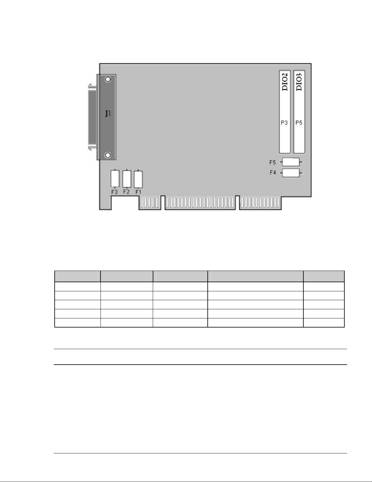
1.5 FUSE AND CONNECTOR PLACEMENT
NOT TO SCALE
Figure 1.3
Fuse and Connector Placement for ADAC/5500 Series Boards.
Fuse # Power Line Fuse Value Manufacturer’s p/n IOtech p/n
F1 -15 V to J1 1.0A, 63 V LITTLEFUSE # 0433001.NR FU-7-1
F2 +15 V to J1 1.0A, 63 V LITTLEFUSE # 0433001.NR FU-7-1
F3 +5 V to J1 1.0A, 63 V LITTLEFUSE # 0433001.NR FU-7-1
F4 +5 V to P3 3.0A, 63 V BUSSMAN # TR/3216-FF-3A FU-7-3
F5 +5 V to P5 3.0A, 63 V BUSSMAN # TR/3216-FF-3A FU-7-3
Note that the ADAC/5500MF does NOT contain the J2 & J3 Aux. Digital I/O connectors
ADAC Series PCI Boards 196 - 6 - ADAC/5500 Series User Manual
908
Page 12
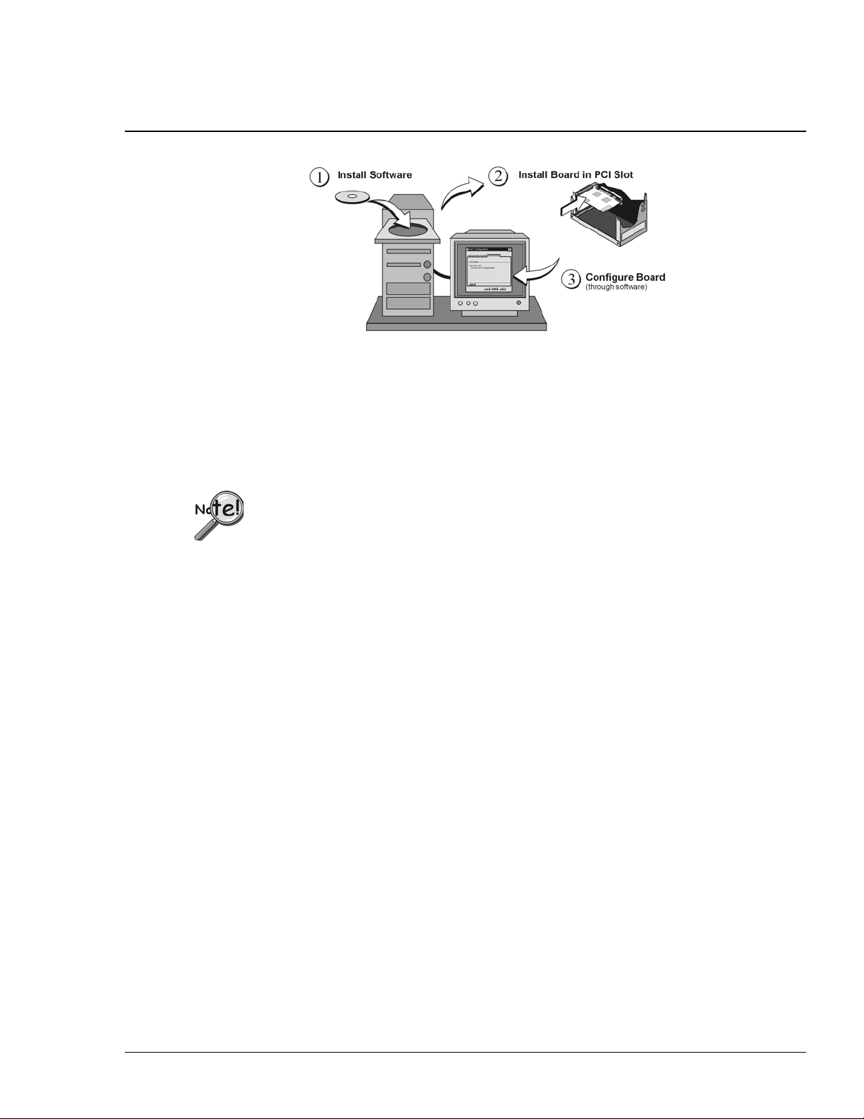
2. GETTING STARTED
This section contains information from the ADAC/5500 Series Inst al lat i o n Guide, p/n 1107-0940. If you have already
installed your software and ADAC board, you shou ld move on to chapter 3, Hardware Configuration.
STEP 1 – INSTALL SOFTWARE
IMPORTANT: Software must be installed before installing hardware.
1. Remove previous version ADAC drivers, if present. You can do this through Microsoft’s
Add/Remove Programs feature.
2. Place the Data Acquisition CD into the CD-ROM drive. Wait for PC to auto-run the CD. This
may take a few moments, depending on your PC. If the CD does not auto-run, use the
Desktop’s Start/Run/Browse feature.
3. After the intro-screen appears, follow the screen prompts.
Upon completing the software installation, continue with step 2, Install Boards in Availab le PCI Bus-
Slots.
ADAC Series PCI Boards 896897 - 7 - ADAC/5500 Series User Manual
Page 13

STEP 2 – INSTALL BOARDS IN AVAILABLE PCI BUS-SLOTS
IMPORTANT: Software must be installed before installing hardware.
Turn OFF power to, and UNPLUG the host PC and externally connected equipment prior
to removing the PC’s cover and installing an ADAC/5500 Series Board. Failure to do so
could result in electric shock, or damage to equipment.
CAUTION
WARNING
Take ESD precautions (packaging, proper handling, grounded wrist strap, etc.)
Use care to avoid touching board surfaces and onboard components. Only handle boards by
their edges (or ORBs, if applicable). Ensure boards do not come into contact with foreign
elements such as oils, water, and industrial particulate.
IMPORTANT: Bus Mastering DMA must be Enabled.
For an ADAC/5500 Series board to operate properly, Bus Mastering DMA must be
enabled on the PCI slot [for which the board is to be installed]. Prior to installation,
verify that your computer is capable of performing Bus Mastering DMA for the
applicable PCI slot. Note that some computers have BIOS settings that enable [or disable]
Bus Mastering DMA. If your computer has this BIOS option, ensure that Bus Mastering
DMA is Enabled on the appropriate PCI slot.
Refer to your PC Owner's Manual for additional informati on reg arding your PC and
enabling Bus Mastering DMA for PCI slots.
1. Turn OFF power to, and UNPLUG the host PC and externally connected equipment.
2. Remove the PC’s cover. Refer to your PC Owner’s Manual as needed.
3. Choose an available PCI bus-slot.
4. Carefully remove ADAC/5500 Series Board from its anti-static protective bag. If you have not already
done so, write down the serial number and type of ADAC board in the space provided on page 3 of this
document.
5. On the PC’s rear panel, loosen and remove the screw for the blank adapte r plate that corresponds with the
chosen PCI bus. See left-hand figure, below.
Removing a Blank Adapter Plate
Installing an ADAC/5500 Series Board
6. Remove the blank adapter plate. Refer to your PC Owner’s Manual if needed.
ADAC Series PCI Boards - 8 - ADAC/5500 Series User Manual
Page 14

7. Align the groove in the ADAC/5500 Series board’s PCI edge-connector with the ridge of the desired PCI
slot. See preceding right-hand figure.
8. Push the board firmly into the PCI slot. The board should “snap” into position.
9. Secure the board by inserting the rear-panel adapter-plate screw.
10. Using the previous steps, install additional boards into available PCI bus-slots, if applicable to your
application.
11. Replace the computer’s cover.
12. Plug in all cords and cables that were removed in step 1.
13. Apply power to, and start up the PC.
Note: At this point some PCs may prompt you to insert an installation disk. While this is rare, if you do
receive such a prompt simply place the install CD-ROM into the disk drive and follow additional
screen prompts.
STEP 3 – CONFIGURE BOARDS
Always turn the computer power OFF and unplug it before connecting or disconnecting a
screw terminal panel or a cable to the PCI card. Failure to do so could result in electric
shock, or equipment damage.
WARNING
Before you can use your ADAC/5500 Series Board, you will need to con figure it according to information
contained in chapters 3 and 4 of this document. However, prior to doing so you may find it helpful to review
the following points:
All configuration, including data-acquisition settings such as analog input, data collection rates,
•
input voltage range, and operating modes are made through ADAC configuration software. The
ADAC configuration software (ADAC Config) file can be accessed from the Windows desktop
Start Menu by navigating as follows:
Start ⇒ Programs ⇒ ADAC ⇒ ADACConfig ⇒ ADAC Config
Desktop Path to ADAC Config
ADAC ADLIB WDM software drivers provide an application level software interface to
•
Windows 98/ME/NT/2000/XP. Software packages such as LabVIEW™ communicate through
our ADLIB driver software. These packages configure and collect, or output, acquisition data in a
GUI based interface.
• The ADAC/5501MF, ADAC/5502MF, ADAC/5503HR and ADAC/5504HR analog inputs are
impedance buffered and drive a differential gain amplifier that can be referenced in a number of
ways, allowing the following programmable input configurations: Single-Ended, Pseudo-
Differential, and Fully-Differential.
ADAC Series PCI Boards 795 - 9 - ADAC/5500 Series User Manual
928
Page 15

•
The ADAC/5500MF analog inputs are impedance buffered. They can only be referenced in SingleEnded input configuration. A 176 element channel-conf iguration RAM is provided to allo w each ADC
channel to be programmed with a different Range. Note that input range selection also applies to
expansion channels located on the ADAC line of accessory screw terminal boards. The termination
boards are detailed in section 4.3.
•
The analog inputs on the ADAC/5500, ADAC/5501MF, ADAC/5502MF, ADAC/5503HR and
ADAC/5504HR may be configured for either ±10 V bipolar or 0-10 V unipolar operation. The input
range is programmable on a channel-by-channel basis in a 176-element channel configuration RAM. Note
that the range selection also applies to expansion channels.
•
The programmable gain circuitry on the ADAC/5501MF, ADAC/5502MF, ADAC/5503HR and
ADAC/5504HR must be taken into account in defining the usable error free input range. The boards
provide a wide range of programmable ranges and resolutions.
•
The ADAC/5500 Series Boards each bring out ±15 V and +5 V to the main I/O connector (J1). In
addition, the ADAC/5501MF, ADAC/5502MF, ADAC/5503HR and ADAC/5504HR bring +5 V to the
auxiliary digital I/O connectors (P3 and P5), located on the backside of those boards. These power lines
are individually fused to protect the ADAC/5500 Series Board. Note that connecting or disconnecting
cables or screw terminal panels (as well as any user connections to these power lines) may blow a fuse, or
cause damage to the board.
•
Incorrect connection of user wiring is one of the most common problems experienced by users of data
acquisition boards. To ensure proper results, you must first determine what type of signal source you are
measuring (Ground Referenced Source or Floating Source), and then choose the appropriate input
configuration on your data acquisition card (Differential, Pseudo-Differential, or S ingle-Ended). Chapter
4 of this manual includes detailed information.
3. HARDWARE CONFIGURATION
The ADAC/5500 Series contains no hardware jumpers; all board configuration elements are software selectable. Dataacquisition settings such as analog input, data collection rates, input voltag e range, and op erating modes are configured
through application software. ADAC ADLIB WDM software drivers provide an application level software interface to
Windows 98/ME/NT/2000/XP. Software packages such as LabVIEW™ communicate through our ADLIB driver
software. These packages configure and collect, or output, acquisition data in a GUI based interface.
3.1 DMA AND INTERRUPT UTILIZATION
The PCI specification uses a shared interrupt scheme to increase the availability of interrupts in an attempt to alleviate
limitations imposed by ISA interrupt constraints. This shared interrupt scheme, known as interrupt chaining, comes at a
price. When a PCI card that uses interrupts is installed into a PC, the system software adds the device to a list of
interrupt service routines for all PCI devices that share a common interrupt signal. When a PCI device generates an
interrupt, the system software detects the interrupt and executes the first Interrupt Service Routin e (ISR) in the list. The
first routine in the list may not be your data acquisition device. If not, th e first device determines if its device asserted
the interrupt, if so the software services the interrupt and returns. The processor immediately interrupts again because
the second device is still generating an interrupt request. The processor again jumps to the first device in the list, the
device determines it has not requested an interrupt and jumps to the entry point of the second ISR to be serviced. If the
first device in the list were to generate interrupts at a high frequency, the second device might over-run or under-run,
generating an error condition while awaiting service. Well-behaved PCI devices generate interrupts infrequently.
ADAC driver software only determines if the ADAC board has requested an interrupt, if so it defers the ISR to a
callback procedure and quickly returns control to the interrupted process. Now that the facts are on the table, interrupt
latency on the PCI bus can be extremely inefficient for high-speed data acquisition. To overcome this inefficiency we
incorporate an on-board DMA engine analogous to the older ISA type of DMA controller. The on-board DMA engine
ADAC Series PCI Boards 795 - 10 - ADAC/5500 Series User Manual 928
Page 16
supports scatter/gather, also known as buffer chaining, with a pair of chain address registers that point to system
memory to be used in the buffered transfer. The DMA controller is loaded with the previously allocated physical
addresses of these buffers and only generates interrupt requests when the current transfer buffer has been completed,
thus reducing the burden of CPU interrupt intervention.
3.2 DMA ENGINE
Both analog input and analog output channels have on-board DMA engine support for high-speed data transfers. The
two analog output channels have individual DMA engines and clocking methods available. DAC1’s clocking source
may be set to the DAC0 clocking source to allow simultaneously DAC transfers. All PCI bus transfers are 32-bit
operations. Analog input and analog output transfers are each independently software selectable to allow either 16-bit
or 32-bit data transfers. An immediate improvement of twice the memory bandwidth can be achieved by transferring
two analog input data points or two analog output data points into memory as a single 32-bit PCI transfer.
3.3 ANALOG INPUT CONFIGURATION
For selecting the best configuration for your application see Section 4.1 Connecting User Wiring.
The ADAC/5501MF, ADAC/5502MF, ADAC/5503HR and ADAC/5504HR an alog inputs ar e impedan ce buffered and
drive a differential gain amplifier that can be referenced in a number of ways allowing th e following programmable
input configurations: Single-Ended, Pseudo-Differential and Fully-Differential.
The ADAC/5500MF analog inputs are impedance buffered, and can only be referenced in Single-Ended input
configuration.
For selecting the best configuration for your application see Section 4.1 Connecting Us er Wiring.
A 176 element channel configuration RAM is provided to allow each ADC channel to be programmed with a
different input range.
3.4 ADC RANGE
The analog inputs on the ADAC/5500, ADAC/5501MF, ADAC/5502MF, ADAC/5503HR and ADAC/5504HR may be
configured for either ±10 V bipolar or 0-10 V unipolar operation. The input range is programmable on a channel by
channel basis in a 176-element channel configuration RAM. Note that the range selection also applies to expansion
channels.
The programmable gain circuitry on the ADAC/5501MF, ADAC/5502MF, ADAC/5503HR and ADAC/5504HR must
also be taken into account in defining the usable error free input range. The boards provide a wide range of
programmable ranges and resolutions. The following tables indicate the maximum resolution under different
conditions. Note that resolution is not accuracy. Resolution defines the minimum definable voltage increment. Absolute
DC accuracy and relative accuracy defines exactly how close the reading will be to the actual voltage input. Refer to
Section 6, SPECIFICATIONS for accuracy specifications.
Fixed Gain
x1 ± 10.00 V 5.00 mV/bit
x1 0 to 10.00 V 2.50 mV/bit
Full Scale Range
Bipolar
Unipolar
Microvolt
Resolution
ADAC Series PCI Boards 795 - 11 - ADAC/5500 Series User Manual 928
Page 17

Programmable
Gain
x1 ± 10.00 V 5.00 mV/bit
x2 ± 5.00 V 2.50 mV/bit
x4 ± 2.50 V 1.25 mV/bit
x8 ± 1.25 V 0.625 mV/bit
x1 0 to 10.00 V 2.50 mV/bit
x2 0 to 5.00 V 1.25 mV/bit
x4 0 to 2.50 V 0.625 mV/bit
x8 0 to 1.25 V 0.3125 mV/bit
Full Scale Range
Bipolar
Unipolar
Microvolt
Resolution
Table 3.2 ADAC/5501MF Input Range/Resolution
Programmable
Gain
x1 ± 10.00 V 5.00 mV/bit
x10 ± 1 V
x100 ±95 mV
X1000 ±9.5 mV
x1 0 to 10.00 V 2.50 mV/bit
x10 0 to 1.00 V
x100 0 to 97.5 mV
X1000 0 to 9.75 mV
Full Scale Range
Bipolar
Unipolar
Microvolt
Resolution
500 µV/bit
50.0 µV/bit
5.00 µV/bit
250 µV/bit
25.0 µV/bit
2.50 µV/bit
Table 3.3 ADAC/5502MF Input Range/Resolution
Programmable
Gain
x1 ± 10.00 V
x2 ± 5.00 V
x4 ± 2.50 V
x8 ± 1.25 V
x1 0 to 10.00 V
x2 0 to 5.00 V
x4 0 to 2.50 V
x8 0 to 1.25 V
Full Scale Range
Bipolar
Unipolar
Microvolt
Resolution
310.140 µV/bit
155.070 µV/bit
77.535 µV/bit
38.768 µV/bit
155.070 µV/bit
77.535 µV/bit
38.768 µV/bit
19.384 µV/bit
Table 3.4 ADAC/5503HR Input Range/Resolution
ADAC Series PCI Boards 795 - 12 - ADAC/5500 Series User Manual 928
Page 18
Programmable
Gain
x1 ± 10.00 V
x10 ± 1 V
x100 ± 99.68 mV
x1 0 to 10.00 V
x10 0 to .1 V
x100 0 to 99.84 mV
Full Scale Range
Bipolar
Unipolar
Microvolt
Resolution
310.140 µV/bit
31.0140 µV/bit
3.10140 µV/bit
155.070 µV/bit
15.5070 µV/bit
1.55070 µV/bit
Table 3.5 ADAC/5504HR Input Range/Resolution
3.5 DAC RANGE
The output range of both DACs are independently programmable to either ±10 V or 0 to 10 V.
The following table indicates the maximum resolution for each available range. Note that resolution is not accuracy.
Resolution defines the minimum definable voltage increment. Absolute DC accuracy and relative accuracy define
exactly how close the actual voltage output will be to the expected output. Refer to Section 6, SPECIFICATIONS, for
accuracy specifications.
Range
Configuration
BIPOLAR ± 10.00 V
UNIPOLAR 0 to 10.00 V
Full Scale Range
Microvolt
Resolution
305.600 µV/bit
152.800 µV/bit
Table 3.6 ADAC/5500 Series Analog Output Range/Resolution
ADAC Series PCI Boards 795 - 13 - ADAC/5500 Series User Manual 928
Page 19

4. EXTERNAL CONNECTIONS
WARNING
Always turn the computer power OFF and unplug it before connecting or disconnecting a screw
terminal panel or a cable to the PCI card. Failure to do so could result in electric shock, or
equipment damage.
The ADAC/5500 cards bring out ±15 V and +5 V to the main I/O connector J1, and +5 V to the auxiliary digital I/O
connectors P3 and P5. These power lines are individually fused to protect the ADAC/5500 card. Connecting or
disconnecting cables or screw terminal panels (as well as any user connections to these power lines) may blow a fuse,
or worse, cause damage to the board. If you are getting incorrect data readings on your ADAC/5500 card, check all
fuses to make sure they have not blown. Replacement fuses can be obtained from the factory, or from most electronics
stores (such as Radio Shack in the USA). Fuse values on the ADAC/5500 card are as follows:
Fuse # Power Line Fuse Value Manufacturer’s p/n IOtech p/n
F1 -15 V to J1 1.0A, 63 V LITTLEFUSE # 0433001.NR FU-7-1
F2 +15 V to J1 1.0A, 63 V LITTLEFUSE # 0433001.NR FU-7-1
F3 +5 V to J1 1.0A, 63 V LITTLEFUSE # 0433001.NR FU-7-1
F4 +5 V to P3 3.0A, 63 V BUSSMAN # TR/3216-FF-3A FU-7-3
F5 +5 V to P5 3.0A, 63 V BUSSMAN # TR/3216-FF-3A FU-7-3
4.1 CONNECTING USER WIRING
Incorrect connection of user wiring is one of the most common problems experienced by users of data acquisition
boards. To ensure proper results, you must first determine what type of signal source you are measuring (Ground
Referenced Source or Floating Source), and then choose the appropriate input configuration on your data acquisition
card (Differential, Pseudo-Differential, or Single-Ended).
4.1.1 Signal Types
Floating Sources
A Floating Source is a signal that has no connection to the building's power ground. Examples of Floating Sources are
batteries, battery powered devices, and signals from optically isolated devices. When connecting Floating Sources to a
data acquisition card, the ground reference of the signal must be tied to the analog ground (AGND) in order to establish
a common reference point.
Ground Referenced Sources
A Ground Referenced Source is one that is connected to the same common ground as the host PC, and therefore has the
same ground as the data acquisition cards. An example is equipment that plugs into the same building power source as
the host PC.
Due to differences in a building's power system, the Ground Referenced Source and the data
acquisition board's ground may be at different voltage levels. This difference is referred to as a
Common Mode Voltage. Common Mode Voltage can be eliminated by using either PseudoDifferential (PD) or Fully-Differential (DI) input configurations on the data acquisition board.
ADAC Series PCI Boards 795 - 14 - ADAC/5500 Series User Manual
928
Page 20

Signal Level
In addition to the grounding of source signals, the maximum voltage level of the signal should be taken into account
when choosing the optimum input configuration on the data acquisition board. When working with signals with a
maximum level below 1 V (Low Level), care must be taken to minimize possible affects caused by noise in the
environment. The addition of noise will have less effect on signals in the 1-10 V range (High Level), and therefore
High Level signals can use more types of input configurations.
4.1.2 Choosing A/D Input Configuration
Once you have determined what type of input signal source you have, and th e voltage level, you then need to select the
proper/optimum input configuration on your data acquisition card:
4.1.2.1 Single-Ended
Applications with a Floating Source are typically wired to a data acquisition board configured for SingleEnded (SE) configuration. Since only one wire from each input signal is connected to a multiplexed input of
the A/D, the Single-Ended configuration provides a larger number of inputs per board than Differential (see
below) configuration. Grounded Signal Sources can be wired in Single-Ended configur ation only when signal
leads are less than 12 feet AND when all signals share a common ground (the signals must be local to one
another).
With the Single-Ended configuration, the input signals are tied to the Channel Hi side of an an alog input, and
all signal low sides are tied to the SGND ground on the data acquisition card.
Single-Ended configuration sh ould only be used when:
• There is no Common Mode Voltage
• Ground isolation is not required
• Signal leads are less than 12 feet.
Note that of all the three possible input configurations, Single-Ended offers the least amount of noise rejection.
Because of this, Low Level signals should only be wired in Single-Ended configuration when you are certain
that there is little or no noise being introduced to the signal from the system, or the environment. We DO NOT
recommend using Single-Ended configuration with Low Level signals.
Figure 4.1 shows proper wiring for Single-Ended configuration.
Figure 4.1
Single-Ended Configuration
ADAC Series PCI Boards 795 - 15 - ADAC/5500 Series User Manual
928
Page 21

4.1.2.2 Pseudo-Differential (PD)
For multiple signal sources that share a common ground (signals must be local to one another), the PseudoDifferential mode may be the most desirable. The Pseudo-Differential configuration is similar to SingleEnded, but the analog low side of each signal is isolated from analog ground (AGND) by a 10 MΩ resistor and
a capacitor. All input returns are tied together to PDIN. Pseudo-Differential configuration allows the system to
reject any common-mode voltage difference that may exist.
Pseudo Differential configuration should be used when:
• Common Mode Voltage exists
• Common Mode Noise does not exist
• Each Source has a local ground
• Input signals are greater than 1 V (High Level)
• Signal leads are longer than 12 feet
Figure 4.2 shows proper wiring for Pseudo-Differential configuration.
4.1.2.3 Fully-Differential (DIFF)
In installations where each Ground Referenced Source signal has a local ground (signal located remote from
one another), the Fully-Differential configuration must be used. Since the Fully-Differential configuration
only responds to the difference in a signal between its high and low vo ltages, an y Co mmon Mod e Voltag e will
be cancelled out. In addition, Fully-Differential configuration provides the best performance of the three
configurations in an electrically noisy environment.
The Fully-Differential configuration should be used when any of the following exists:
• Each source has a local ground
• Signal sources are remote from one another
• Common Mode Voltage exists
• Common Mode Noise exists
• Signal sources are low-level (less than 1 V)
• Signal source leads are longer that 12 feet
Figure 4.2
Pseudo-Differential Configuration
ADAC Series PCI Boards 795 - 16 - ADAC/5500 Series User Manual
928
Page 22

Fully-Differential for Grounded Signal Sources
See Figure 4.3 for an example of connecting Grounded Signal Sources in Fully Differential configuration.
Figure 4.3
Fully-Differential Configuration for Grounded Sources
Fully-Differential for Floating Signal Sources
Floating Signal Sources are typically wired to a data acquisition board in Single-Ended configuration,
however, when the Floating Source signal leads pass through an electrically noisy environment, FullyDifferential configuration will give the best performance. When wiring Floating Signal sources in FullyDifferential configuration, a resistor must be connected from the low side of the sources to analog ground
(AGND). These resistors create a return path to AGND for the bias currents of the instrumentation amplifier.
If a return path is not provided, the bias current will build up on stray capacitance, resulting in drift and
possible saturation of the amplifier.
If the input signal is DC coupled a 10 K ohm to 100 K ohm resistor must be connected from the input signal's
return to the data acquisition board's AGND.
For AC coupled input signals a 10 K ohm to 100 K ohm resistor must be connected from both input signal
high and input signal low to AGND.
ADAC Series PCI Boards 795 - 17 - ADAC/5500 Series User Manual
928
Page 23

Figure 4.4 shows how to properly wire a Floatin g Source Signal in Fully-Differential configuration. In the
case where there is a combination of Ground Referenced Sources and Floating Sources, the Fully-Differential
mode should be used.
Figure 4.4
Fully-Differential Configuration for Floating Sources
4.2 MAIN I/O CONNECTOR (J1)
The main board connector is a 68 pin “SCSI III” style connector. This connector carries all the Analog I/O connections
as well as the 16 Digital I/O connections.
The ADAC/5500 input channels may be connected directly to any High Level voltage source. If long leads are run
from transducers to the system, it is very important that the leads be shielded to protect against pickup of power
frequency and other noise.
The factory has a line of screw terminal panels which can be used to ease field wiring to the PCI cards. Any of these
panels may be connected to the PCI card with an SCSC-III type cable (which can be ordered from the factory as a G55
cable).
The ADAC line of screw terminal panels includes:
ADAC-TB-8 - For use with the ADAC/5500MF boards only, this panel provides access to the 8 on-board analog input
channels, as well as the DIO ports 0 and 1 and various clocking and triggering signals.
ADAC-TB-16 - For use with the ADAC/5501MF, ADAC/5501MF-V, ADAC/5502MF, ADAC/5503HR,
ADAC/5503HR-V, and ADAC/5504HR boards only, this panel provides access to the 16 on-board analog input
channels, as well as the DIO ports 0 and 1, various clocking and triggering signals, and two optional DACs.
4.2.1 Signal Definitions
The following is a description of each of the signals available at the J1-pin connector at the front edge of the board.
ADAC Series PCI Boards 795 - 18 - ADAC/5500 Series User Manual
928
Page 24

4.2.1.1 Analog Input Channels
These channel signals are over-voltage protected to 20 V above or below the ±15 V power supply. The
channel inputs can withstand input voltages of up to ±20 volts when the power to the system is off.
ADAC-TB-8
CH 0..CH 7 - These signals are the positive half of the associated single-ended input channels.
ADAC-TB-16
CH 0..CH 14 EVEN - These signals are either the positive half of th e associated differential input
channel pairs 0 through 7, or single-ended/pseudo-differential input channels 0 through 14 even.
CH 1..CH 15 ODD - These signals are either the negative half of the associated differential input
channel pairs 0 through 7, or single-ended/pseudo-differential input channels 1 through 15 odd.
4.2.1.2 Analog Outputs
DAC 1, DAC 0 - These signals are the voltage output signals from the optional DACs.
RTN 1, RTN 0 - These signals are the return lines for the voltage outputs. These inputs are
essentially tied to AGND (Analog Ground) on the board.
4.2.1.3 Digital I/O Lines
DIO 0..DIO 15 - These signals are the 16 TTL level digital controls lines configurable as 8 bit input
or output lines. These lines are not clocked.
4.2.1.4 Terminal Panel Control
These signals are used to control the various optional terminal panels. The function of some signals may vary
slightly depending on the panel used.
MUX 0..MUX 7 - These signals are used to control the external multiplexers on active panels. These
lines directly reflect the current state of the Channel RAM bits of the same name.
ADCLKIN - This is the ADC External Pacer clock input. This input recognizes TTL level signals
and is edge sensitive. The active edge is selectable as either rising or falling.
The ADCLKIN signal line is shared with the on-board COUNTER 0 Clock Input
signal (CNTR0) pin #39 on the 68-pin J1 connector. Therefore only one input signal
may be connected to the ADCLKIN / CNTR0 terminal at any given time. Attempting to use COUNTER 0 when the ADC Pacer Clock Source is set for an External
Clock Input would not be possible, unless COUNTER 0 was being used to count the
ADC’s External Clock Input signal.
ADCLKOUT - This signal is the ADC’s External Clock Output. Each time the ADC is clocked from
any of the available clocking sources the ADCLKOUT signal pulses high for a period of 1
microsecond. This output can be used to synchronize multiple A/D converters on different PCI cards
allowing simultaneous A/D conversions by connecting the ADCLKOUT to the ADCLKIN input of
each PCI card.
ADAC Series PCI Boards 795 - 19 - ADAC/5500 Series User Manual
928
Page 25

The ADCLKOUT signal line is shared with the on-board TIMER 1 Clock Output
signal (TMR1) pin #5 on the 68-pin J1 connector. Therefore only one output signal
may be generated to the ADCLKOUT / TMR1 terminal at any given time. The
TIMER 1 is automatically disabled in hardware when the ADCLKOUT is enabled.
ADTGIN - This is the External ADC Trigger/Gate input. This input recognizes TTL level signals
and is used to start or stop the ADC acquisition process. The input is selectable as either rising/falling
edge or active high/low level sensitivity.
ADTGOUT - This signal is the internal ADC’s Trigger output. Each time the ADC is triggered from
any of the available triggering sources the ADTGOUT signal pulses high for a period of 1
microsecond. This output can be used to synchronize multiple A/D converters on different
ADAC/5500 cards allowing simultaneous A/D triggering by connecting the ADTGOUT to the
ADTGIN input of each PCI card.
The ADTGOUT signal line is shared with the on-board TIMER 0 Clock Output
signal (TMR0) pin #4 on the 68-pin J1 connector. Therefore only one output signal
may be generated to the ADTGOUT / TMR0 terminal at any given time. The
TIMER 0 is automatically disabled in hardware when the ADTGOUT is enabled.
DACLKIN - This is the External DAC0 Pacer clock input. This input recognizes TTL level signals
and is edge sensitive. The active edge is selectable as either rising or falling.
The DACLKIN signal line is shared with the on-board COUNTER 1 Clock Input
signal (CNTR1) pin #40 on the 68-pin J1 connector. Therefore only one input signal
may be connected to the DACLKIN / CNTR1 terminal at any given time. Attempting to use COUNTER 1 when the DAC Pacer Clock Source is set for an External
Clock Input would not be possible unless COUNTER 1 was being used to count the
DAC’s External Clock Input signal.
DATGIN - This is the External DAC0 Trigger/Gate input. This input recognizes TTL level signals
and is used to start or stop the DAC acquisition process. The input is selectable as either rising/falling
active edge or active high/low level sensitivity.
4.2.1.5 Counters And Timers
CNTR0 - This is the general purpose Counter 0 clock input. This input recognizes TTL level signals
and is rising edge sensitive. The input clock rate cannot exceed 500 kHz. The clock source must
provide a minimum pulse width of 100 ns.
The COUNTER 0’s External Clock Input line (CNTR0) is shared with the ADC’s
External Clock Input signal (ADCLKIN) pin #39 on the 68-pin J1 connector.
Therefore only one input signal may be connected to the ADCLKIN / CNTR0
terminal at any given time. Attempting to use COUNTER 0 when the ADC Pacer
Clock Source is set for an External Clock Input would not be possible, unless
COUNTER 0 was being used to count the ADC’s External Clock Input signal.
ADAC Series PCI Boards 795 - 20 - ADAC/5500 Series User Manual
928
Page 26

CNTR1 - This is the general purpose Counter 1 clock input. This input recognizes TTL level signals
and is rising edge sensitive. The input clock rate cannot exceed 500 kHz. The clock source must
provide a minimum pulse width of 100 ns.
The COUNTER 1’s External Clock Input line (CNTR1) is shared with the DAC’s
External Clock Input signal (DACLKIN) pin #40 on the 68-pin J1 connector.
Therefore only one input signal may be connected to the DACLKIN / CNTR1
terminal at any given time. Attempting to use COUNTER 1 when the ADC Pacer
Clock Source is set for an External Clock Input would not be possible, unless
COUNTER 1 was being used to count the DAC’s External Clock Input signal.
TIMER0 - This LSTTL output signal provides a 50% duty cycle square wave derived from an
independent TMR0 internal software pacer clock. The pacer clock period can be set from 1 us to
65535 us, producing an output clock rate from 500 KHz down to approximately 7.6295 Hz.
The TIMER 0’s External Clock Output line (TMR0) is shared with the ADC’s
External Trigger Output signal (ADTGOUT) pin #4 on the 68-pin J1 connector.
Therefore only one output signal may be generated to the ADTGOUT / TMR0
terminal at any given time. TIMER 0 is automatically disabled in hardware when
the ADC’s External Trigger Output is enabled.
TIMER1 - This LSTTL output signal provides a 2nd clock source, with characteristics identical to
TIMER0, using a separate, independent, TMR1 internal software pacer clock.
4.2.1.6 Ground Lines
SGND - This signal is the reference ground used for A/D conversion s. If you are measuring from a
fully floating source in differential mode, it would be beneficial to tie one of the channel inputs to this
point. This signal should not be used for sinking large amounts of current. This signal also acts as the
common reference line when the board is configured for single-ended inputs.
PDIN - This signal is the common return line used when the board is configured for pseudo
differential input mode.
AGND - This signal is the power return for the ±15 V power supply lines. It is distinguished from the
DGND line because it generally helps separate the poten tially high frequency digital ground noise
from the analog circuits that are powered by ±15 V.
DGND - This signal is the +5 V power return line. It is generally noisier than AGND and is a good
logic low reference point.
4.2.1.7 Power Lines
+15 V, -15 V - This power is only intended to power the optional terminal panels with active
circuitry on them. These voltages are supplied by one of the on-board DC/DC converters.
Approximately ±30 mA are available on these lines. Both lines are fused
@ 125 mA.
The TIMER 1’s External Clock Output line (TMR1) is shared with the ADC’s
External Clock Output signal (ADCLKOUT) pin #5 on the 68-pin J1 connector.
Therefore only one output signal may be generated to the ADCLKOUT / TMR1
terminal at any given time. TIMER 1 is automatically disabled in hardware when
the ADC’s External Clock Output is enabled.
+5 V - This signal is sourced directly from the PCI Bus. Take great care when using this power.
These lines are fused @ 3 Amps.
ADAC Series PCI Boards 795 - 21 - ADAC/5500 Series User Manual
928
Page 27

(
)
4.2.2 J1 Pin Assignments For ADAC/5500MF Only
Standard 68-Pin SCSCI Type III, Socket (Female) Connector with Orb
Pin
Signal
Description /
Pin
Signal
Description / Comments
Comments
1 DGND Digital Ground 35 +5 V (fused) Power
2 +15 V (fused) Power 36 +5 V
3 -15 V (fused) Power 37 +5 V (fused) Power
4 ADTGOUT / TMR0 Internal ADC Trigger Output
/ Timer 0 Clock Output
5 ADCLKOUT / TMR1 Internal ADC Trigger Output
/ Timer 1 Clock Output
6 N/C Not Connected 40 CNTR1 Counter 1 Clock Input
7 DIO_15 TTL Level Digital I/O Ch. 15 41 DIO_14 TTL Level Digital I/O Ch. 14
8 DIO_13 TTL Level Digital I/O Ch. 13 42 DIO_12 TTL Level Digital I/O Ch. 12
9 DIO_11 TTL Level Digital I/O Ch. 11 43 DIO_10 TTL Level Digital I/O Ch. 10
10 DIO_9 TTL Level Digital I/O Ch. 9 44 DIO_8 TTL Level Digital I/O Ch. 8
11 DIO_7 TTL Level Digital I/O Ch. 7 45 DIO_6 TTL Level Digital I/O Ch. 6
12 DIO_5 TTL Level Digital I/O Ch. 5 46 DIO_4 TTL Level Digital I/O Ch. 4
13 DIO_3 TTL Level Digital I/O Ch. 3 47 DIO_2 TTL Level Digital I/O Ch. 2
14 DIO_1 TTL Level Digital I/O Ch. 1 48 DIO_0 TTL Level Digital I/O Ch. 0
15 DGND Digital Ground 49 N/C Not Connected
16 N/C Not Connected 50 N/C Not Connected
17 N/C Not Connected 51 N/C Not Connected
18 N/C Not Connected 52 N/C Not Connected
19 N/C Not Connected 53 N/C Not Connected
20 N/C Not Connected 54 N/C Not Connected
21 AGND Analog Ground 55 AGND Analog Ground
22 N/C Not Connected 56 N/C Not Connected
23 SGND Signal Ground 57 N/C Not Connected
24 N/C Not Connected 58 N/C Not Connected
25 AIN_7 Analog Input, Ch. 7 59 AIN_3 Analog Input, Ch. 3
26 N/C Not Connected 60 N/C Not Connected
27 AIN_6 Analog Input, Ch. 6 61 AIN_2 Analog Input, Ch. 2
28 N/C Not Connected 62 N/C Not Connected
29 AIN_5 Analog Input, Ch. 5 63 AIN_1 Analog Input, Ch. 1
30 N/C Not Connected 64 N/C Not Connected
31 AIN_4 Analog Input, Ch. 4 65 AIN_0 Analog Input, Ch. 0
32 N/C Not Connected 66 N/C Not Connected
33 N/C Not Connected 67 N/C Not Connected
34 AGND Analog Ground 68 DGND Digital Ground
38 ADTGIN External Gate (level controlled),
39 ADCLKIN / CNTR0 External ADC Clock In, or
fused
Power
or External Trigger (edge active)
Counter 0. Rising or Falling
Edge Sensitive.
ADAC Series PCI Boards 795 - 22 - ADAC/5500 Series User Manual
928
Page 28

(
)
4.2.3 J1 Pin Assignments for ADAC/5501MF, ADAC/5502MF, ADAC/5503HR, & ADAC/5504HR
Standard 68-Pin SCSCI Type III, Socket (Female) Connector with Orb
Pin
1 DGND Digital Ground 35 +5 V (fused) Power
2 +15 V (fused) Power 36 +5 V
3 -15 V (fused) Power 37 +5 V (fused) Power
4 ADTGOUT / TMR0 Internal ADC Trigger Output /
5 ADCLKOUT /
6 DATRIGIN DAC0 External Gate (Level
7 DIO_15 TTL Level Digital I/O Ch. 15 41 DIO_14 TTL Level Digital I/O Ch. 14
8 DIO_13 TTL Level Digital I/O Ch. 13 42 DIO_12 TTL Level Digital I/O Ch. 12
9 DIO_11 TTL Level Digital I/O Ch. 11 43 DIO_10 TTL Level Digital I/O Ch. 10
10 DIO_9 TTL Level Digital I/O Ch. 9 44 DIO_8 TTL Level Digital I/O Ch. 8
11 DIO_7 TTL Level Digital I/O Ch. 7 45 DIO_6 TTL Level Digital I/O Ch. 6
12 DIO_5 TTL Level Digital I/O Ch. 5 46 DIO_4 TTL Level Digital I/O Ch. 4
13 DIO_3 TTL Level Digital I/O Ch. 3 47 DIO_2 TTL Level Digital I/O Ch. 2
14 DIO_1 TTL Level Digital I/O Ch. 1 48 DIO_0 TTL Level Digital I/O Ch. 0
15 DGND Digital Ground 49 CJ2 Reserved
16 CJ1 Reserved 50 CJ0 Reserved
17 MUX7 Reserved 51 MUX6 Reserved
18 MUX5 Reserved 52 MUX4 Reserved
19 MUX3 Reserved 53 MUX2 Reserved
20 MUX1 Reserved 54 MUX0 Reserved
21 AGND Analog Ground 55 AGND Analog Ground
22 ADEX_LO Reserved, AD Expansion LO 56 ADEX_HI Reserved, AD Expansion HI
23 SGND Signal Ground 57 PDIN Pseudo-Differential Input return
24 AIN_15 Analog Input, Ch. 15 58 AIN_7 Analog Input, Ch. 7
25 AIN_14 Analog Input, Ch. 14 59 AIN_6 Analog Input, Ch. 6
26 AIN_13 Analog Input, Ch. 13 60 AIN_5 Analog Input, Ch. 5
27 AIN_12 Analog Input, Ch. 12 61 AIN_4 Analog Input, Ch. 4
28 AIN_11 Analog Input, Ch. 11 62 AIN_3 Analog Input, Ch. 3
29 AIN_10 Analog Input, Ch. 10 63 AIN_2 Analog Input, Ch. 2
30 AIN_9 Analog Input, Ch. 9 64 AIN_1 Analog Input, Ch. 1
31 AIN_8 Analog Input, Ch. 8 65 AIN_0 Analog Input, Ch. 0
32 RTN1 Voltage output return, line 1. 66 DAC1 (Note 2) Digital-to-Analog Converter 1
33 RTN0 Voltage output return, line 0. 67 DAC0 (Note 1) Digital-to-Analog Converter 0
34 AGND Analog Ground 68 DGND Digital Ground
Signal
TMR1
Description / Comments
Timer 0 Clock Output
Internal ADC Trigger Output /
Timer 1 Clock Output
Controlled), or External
Trigger (Edge Active).
Pin
38 ADTGIN External Gate (level controlled), or
39 ADCLKIN / CNTR0 External ADC Clock In, or Counter
40 DACLKIN / CNTR1 External ADC Clock In, or Counter
Signal
fused
Description / Comments
Power
External Trigger (edge active)
0. Rising or Falling Edge
Sensitive.
0. Rising or Falling Edge
Sensitive.
Note 1: The clock source of the primary DAC0 channel may be software command, DAC0 Pacer clock,
or an external event (DACLKIN).
Note 2: The clock source of the secondary DAC1 channel may be software command, DAC1 Pacer clock, or Channel 0
clock source.
ADAC Series PCI Boards 795 - 23 - ADAC/5500 Series User Manual
928
Page 29

4.2.4 P3 and P5 Pin Assignments
The ADAC/5501MF, ADAC/5502MF, ADAC/5503HR and ADAC/5504HR include two auxiliary 40-pin headers.
These are located on the back of the boards, and provide access to the two 16-bit DIO ports (DIO2 and DIO3). Two
CA-G17-ADAC cables can be used to bring the DIO2 and DIO3 headers to separate37-pin D-type connectors [one
GA-17 cable per DIO header]. GA17’s orb (following figure) mounts at the back of the host PC.
The DB37-end of a CA-G17-ADAC Cable, which includes an Orb for PC Mounting
SIGNAL NAME P3 PIN or
P5 PIN
DGND 1 1 DGND 21 11
+ 5 V (fused) 2 20 D9 22 30
DGND 3 2 DGND 23 12
D0 4 21 D10 24 31
DGND 5 3 DGND 25 13
D1 6 22 D11 26 32
DGND 7 4 DGND 27 14
D2 8 23 D12 28 33
DGND 9 5 DGND 29 15
D3 10 24 D13 30 34
DGND 11 6 DGND 31 16
D4 12 25 D14 32 35
DGND 13 7 DGND 33 17
D5 14 26 D15 34 36
DGND 15 8 DGND 35 18
D6 16 27 STROBE2 / 3 36 37
DGND 17 9 DGND 37 19
D7 18 28 DGND 38 n/c
DGND 19 10 DGND 39 n/c
D8 20 29 DGND 40 n/c
G17 PIN
(37-pin D)
SIGNAL NAME P3 PIN or
P5 PIN
G17 PIN
(37-pin D)
P3 & P5 Auxiliary Digital I/O Connectors
Standard 40-Pin Male Headers
A CA-G17-ADAC Cable, Installed
Signal definitions for the P3 and P5 Auxiliary 40-Pin DIO headers and the DB37 connector follow.
ADAC Series PCI Boards 795 - 24 - ADAC/5500 Series User Manual
928
Page 30

4.2.5 Signal Definitions for P3, P5, and GB17’s DB37 Connector
The following descriptions apply to each of the signals that are available at the 40-pin auxiliary DIO headers,
designated as P3 and P5. The headers are located on the back of boards: ADAC/5501MF, ADAC/5502MF,
ADAC/5503HR, and ADAC/5504HR. In addition, the signals apply to the correspond ing pins on GA17’s
DB37 connector as indicated in the table on the preceding page.
GA17’s orb (following figure) mounts at the back of the host PC.
The DB37-end of a CA-G17-ADAC Cable, which includes an Orb for PC Mounting
D0... D15 These signals are the sixteen 5 V CMOS/LSTTL level digital input/output lines of DIO2 on
connector P3, and the D103 connector on P5.
On G17’s DB37 connector, D0 through D15 correspond to pins 21 through 36, with DB0
assigned to pin 21, DB1 assigned to pin 22, DB2 assigned to pin 23, etc.
DGND This signal is the +5 V power return line. It may also be used as a reference ground for TTL
signals. On G17’s DB37 connector, the DGND lines connect to pins 1 through 19,
inclusive.
+5 V This signal is +5 V power voltage signal that is sourced directly from the PC bus. The +5 V
lines are fused at 3 amps. See WARNING. On G17’s DB37 connector, the +5 V power
signal corresponds to pin 20.
WARNING
Possible electric shock. Take great care when using the +5 V power as the
voltage signal is sourced directly from the PC Bus. The +5 V lines are
fused at 3 Amps.
STROBE The Strobe2 signal is provided on the DIO2 37-pin interface and the Strobe3 signal is
provided on the DIO3 interface. When either port is configured as an input port, the
associated Strobe signal is disabled and placed in a High Impedance state (Z off). When
DIO port is configured as an output port, the associated strobe signal will be pulsed low for
1 microsecond following each data output event that occurs.
On system power-up the DIO Strobe signals are disabled and placed in a High Impedance
state (Z off). 3.3 V CMOS signal.
In regard to the G17 DB37 connector, pin-3 7 is use d fo r th e strobe si g nal.
ADAC Series PCI Boards 795 - 25 - ADAC/5500 Series User Manual
928
Page 31

4.3 SCREW-TERMINAL BOARDS
4.3.1 ADAC-TB-8 Screw-Terminal Board Connections
The ADAC-TB-8 provides screw-terminal access to all of a ADAC/5500MF board’s analog and
digital I/O signals. The terminal board connects to the ADAC/5500MF via a 3-foot long 68-pin
conductor expansion cable, p/n CA-G55-ADAC. The terminal board accepts wire up to 14 AWG.
ADAC-TB-8
WARNING
Always turn the computer power OFF and unplug it before connecting or
disconnecting a screw terminal panel or a cable to the PCI card. Failure to do
so could result in electric shock, or equipment damage.
ADAC Series PCI Boards 795 - 26 - ADAC/5500 Series User Manual
928
Page 32

4.3.2 ADAC-TB-16 Screw-Terminal Board
One ADAC-TB-16 provides screw-terminal access to all analog and digital I/O signals from any one of the
following boards: ADAC/5501MF, ADAC/5501MF-V, ADAC/5503HR, and ADAC/5503HR-V. The
terminal board connects to the board via a 3-foot long 68-pin conductor expansion cable, p/n CA-G55-ADAC.
The terminal board accepts wire up to 14 AWG.
ADAC-TB-16
WARNING
Always turn the computer power OFF and unplug it before connecting or
disconnecting a screw terminal panel or a cable to the PCI card. Failure to do
so could result in electric shock, or equipment damage.
ADAC Series PCI Boards 795 - 27 - ADAC/5500 Series User Manual
928
Page 33

4.3.3 ADAC-DC-37 Screw-Terminal Board for Auxiliary Digital I/O
The ADAC-DC-37 provides access to 16 of the 32 available auxiliary digital I/O channels from
ADAC/5501MF, ADAC/5501MF-V, ADAC/5503HR, and ADAC/5503HR-V boards. Two ADACDC-37 terminal boards are required to access all 32 digital I/O channels.
As depicted on page 4, each DC-37 terminal board can connect to an ADAC/5500 Series Board via a
CA-G17-ADAC cable, or to an optional CA-G37-x-ADAC extension cable, which interfaces
between a CA-G17 cable’s orb and the ADAC-DC-37 board.
ADAC-DC-37
WARNING
Always turn the computer power OFF and unplug it before connecting or
disconnecting a screw terminal panel or a cable to the PCI card. Failure to do
so could result in electric shock, or equipment damage.
ADAC Series PCI Boards 795 - 28 - ADAC/5500 Series User Manual
928
Page 34

5. ADAC/5500 SERIES PCI CARD OPERATION
5.1 DEVICE DRIVERS
The simplest method of operating the card is by using a program package such as LabVIEW™. This package can be
incorporated to do a wide range of display, data logging and control functions. For those who prefer to write their own
programs, the ADAC/5500 cards include the ADAC ADLIB WDM Series of driver packages. These packages provide
easy to use software function calls that can be used to perform most available board functions
5.1.1 LabVIEW™
The ADAC/5500 cards are fully supported by the ADAC-LVi data acquisition VIs for LabVIEW™. Please refer to the
ADAC-LVi manual (p/n 1107-0901) for details on using ADAC cards with LabVI EW™. The ADAC-LVi software and
user manuals are included on the ADAC CD that ships with the ADAC/5500 boards. Follow the instructions on the CD
for proper installation.
5.1.2 TestPoint™
The ADAC/5500 cards are fully supported by the TestPoint software. Please refer to the TP Help manual for details on
using ADAC cards with TestPoint. The TestPoint driver software and user help manual are included on the ADAC CD
that ships with the ADAC/5500 boards. Follow the instructions on the CD for proper installation. Note that the ADAC
driver software is also included with new releases of the TestPoint software. The TP ADAC-32 User’s Manual is p/n
1107-0903.
5.1.3 Windows Drivers (ADLIB WDM)
ADLIB WDM is a set of sophisticated, high level, dynamically linked library (DLL) data acquisition subroutines for
programmers involved in the developing of process and/or data acquisition applications. ADLIB WDM is both a
Microsoft C interface library (C, Visual C++) and a Visual Basic interface library for Windows 98/ME/NT/2000/XP.
The functions supplied with ADLIB WDM provide an easy to use interface to the line of PC data acquisition products,
shielding the programmer from the complexity of low level DAQ board programming and complicated DMA and
interrupt handling mechanisms of the PC and the Windows environment. Based on Microsoft’s Windows Driver
Model, ADLIB WDM supports DMA, Interrupt and Software Po lled data transfer methods for acquiring da ta. ADLIB
WWDM has full support for analog high level (10 V) and analog low level (mV) inputs.
The ADLIB WDM software and user manuals are inclu ded on the ADAC CD that ships with the ADAC/5500 boards.
Follow the instructions on the CD for proper installation.
ADAC Series PCI Boards 795 - 29 - ADAC/5500 Series User Manual 928
Page 35

5.2 THEORY OF OPERATION
5.2.1 Process Definitions
In order to best understand how to operate the various board functions, it is important to first understand the language
that will be used to describe the board processes. The following is a list of pertinen t terms and definitions used in this
document.
ADC
Analog to Digital Converter, also referred to as A/D. This is the circuitry that samples the voltage present at one of the
inputs and translates that reading to a number that is representative of the input voltage. The number supplied by the
ADC is referred to as the ADC DATA or RAW DATA and its units are bits or binary digits.
DAC
Digital to Analog Converter, also referred to as D/A. This is the circuitry that translates a binary data word to a specific
voltage level. The optional DACs on the ADAC/5500 Series boards are specified for DC accuracy. The DACs on these
boards can be clocked and triggered; the outputs are updated as soon as they receive new data.
ADC Channel
This term is used to refer to any of the 256 addressable connections to the multiplexed ADC. The ADAC/5 500MF has
8 on-board ADC channels available and supports the ADAC-TB-8 panel. The ADAC/5501MF, ADAC/5502MF,
ADAC/5503HR and ADAC/5504HR have 16 on-board channels available and support the ADAC-TB-16 and ADACTB-8 panels for a maximum number of 256 input channels.
ADC Data- also Raw Data
This is the unscaled number returned by the ADC. For two’s complement data coding (which is standard for bipolar
inputs), this number will be either in the range of -2000...+1999 (for 12-bit A/D boards) or -32242…+32241 (for 16-bit
boards). For straight binary data coding (which is standard for unipolar inputs), this number will be in th e range of
0..+3999 on 12-bit A/D boards and 0...+644 83 on 16-bit boards. This number is typically multiplied by some scale
factor to convert the number to more useful engineering units. For example: the bipolar ±10 V input uses a scale factor
of .005 V/bit. An ADC reading of +1000 when multiplied by .005 V results in +5 .000 V. Similarly, the 16 bit scale
factor for the ±10 V scale is .000130140 V/bit.
DAC Data- also Raw Data
This is the unscaled number sent to each DAC channel. For two’s complement data coding (which is standard for
bipolar inputs), this number will be either in the range of -32722...+32722. For straight binary data coding (which is
standard for unipolar inputs), this number will be in the range of 0..+65445. This number is typically multiplied by
some scale factor to convert the number to more useful engineering units. For example: 0-10 V input uses a scale factor
of .000152800V/bit. A DAC DATA value of 32723 when multiplied by .0001528 0 results in 5.000044 V at the DAC
output line.
ADC Conversion
This is the process of sampling a single input or transducer’s voltage and generating a representative data value.
DAC Conversion
This is the process of outputting a single voltage generated from representative data value.
ADAC Series PCI Boards 795 - 30 - ADAC/5500 Series User Manual 928
Page 36

ADC Acquisition
This term is used to refer to a series of A/D conversions. This series may consist of sampling a single channel several
times or sampling several channels sequentially one or more times. An acquisition has a clearly defined Starting point
and Ending point. Thus an acquisition may be STARTED and STOPPED.
DAC Acquisition
This term is used to refer to a series of D/A conversions. This series may consist of outputting a sing le DAC channel
several times or outputting both channels simultaneously one or more times. An acquisition has a clearly defined
Starting point and Ending point. Thus an acquisition may be STARTED and STOPPED.
ADC and DAC Clock
This is the signal or impetus that initiates an A/D or D/A conversion. To CLOCK the ADC or DAC is to start an A/D
conversion. The term clock is used for this process because typically a clock signal consists of a series of pulses that are
periodic or evenly timed. If the conversions are evenly spaced it is then possible to digitally reconstruct the input
waveform without distorting its component frequencies.
ADC and DAC PACER Clock
This is a timed periodic signal that may either directly clock the ADC/DAC or initiate a burst of ADC conversions.
Thus the PACER clock is exclusive to both the ADC and DAC channels.
ADC BURST Clock
This is also a timed periodic signal that may be used to directly clock the ADC. When the Burst clock is used, this
signal defines the time between individual conversions. This signal is not, however, continuous. It lasts for a predefined
number of pulses and then stops. The duration of this signal is called the burst clock; and the period of individual pulses
is the burst rate. The ADC Pacer Clock initiates Bursts.
ADC and DAC Trigger
This is the signal or impetus that initiates or terminates an Acquisition. Essentially the Trigger Starts o r Stops the ADC
or DAC PACER Clock.
ADC Channel Configuration RAM
This is the term used for the ADC’s Channel, Gain, Range, and Input Configuration lookup table. The length of this
table can be anywhere from 1 element to 176 elements. When an ACQUISITION is in process, the board will
sequentially go through this list to determine the channel and gain setting fo r the next conversion. Thus, channels may
be sampled in any order and at any gain. Note, however, that for maximum performance, it is recommended that
channels with like gains be grouped together in the sample sequence.
ADC Polled
This is an acquisition mode in which all aspects of the data collection is handled directly. Specifically, once an A/D
conversion is initiated, the software must POLL the ADC’s status register testing for a DATA available flag to set and
data is then read from the board. This mode requires the most software overhead.
DAC Polled
This is an acquisition mode in which all aspects of the data collection is handled directly. Specifically, once a D/A
conversion is initiated, the software must POLL the DAC’s status register testing for a DATA ready flag to set before
the next DAC conversion can be initiated. This mode requires the most software overhead.
ADAC Series PCI Boards 795 - 31 - ADAC/5500 Series User Manual 928
Page 37

ADC and DAC DMA
Short for Direct Memory Access, DMA is the most self-sufficient of the Acquisition Modes available over the PCI bus.
In this mode, data from each conversion is automatically transferred directly from the ADAC/5500 board to or from
some pre-specified block of system memory. Essentially, DMA allows the acquisition process to run in the b ackground
with virtually no software overhead.
5.2.2 Clocking the ADC
The source of the ADC clock may be any of the following:
1) Software Command
2) Pacer Clock
3) External Event (ADCLKIN)
4) Burst Clock
Once an ADC clock is received, the Analog input is immediately sampled. Converted data will become available
within 10 microseconds of the clock (max) for 12-bit boards, and 5 microseconds (max) for 16-bit boards. Any attempt
to clock the ADC while an A/D conversion is currently running will result in a Clock Error.
5.2.2.1 ADC Software Generated Single Clock
A single A/D conversion may be initiated by a software generated clock. The ADC will sample the voltage
present on the channel selected by the Channel configuration RAM. After issuing the software convert
command, the FNE
1
flag in the AD_STATUS register is monitored to determine when the conversion has
completed, and data is available to be read out of the AD_FIFO register.
5.2.2.2 ADC Pacer Clocking
A series of A/D conversions may be controlled by the on-board pacer clock. This timer can be programmed to
generate a periodic clock rate up to the ADC’s maximum rate or as slow as 4 samples per hour.
5.2.2.3 ADC External Event Clocking
Conversions may also be caused by an external event. ADCLKIN is an edge sensitive input that can be
programmed to cause conversions. The ADCLKIN is selectable as either rising or falling edge sensitive.
5.2.2.4 ADC Burst Clocking
This mode uses the Burst Rate clock to initiate conversions. The Burst Rate is defined as the time between
ADC conversions and the duration of the burst is defined Burst Length. When burst mode is enabled, each
burst will be started by any of the three previously mentioned clock sources.
5.2.2.5 ADC Maximum Clock Rate
The maximum rate which the ADC should be clocked and retain optimal accuracy will vary depending on
several factors. These include ADC resolution (12 or 16-bits), gain setting, and sampling mode.
The first limiting factor is the ADC chip itself. Boards with 12-bit ADC chips are capable of performing
analog to digital conversions at up to 100 kilo-samples per second. Models with 16-bit ADC chips will sample
at rates up to 200 kilo-samples per second. These limits may not be exceeded. If the sample clock is run faster,
some of the clock pulses will be ignored by the circuitry, and a clock error will be generated.
1
FIFO and DMA control bits and ADC status flags are grouped together in the AD_STATUS register.
ADAC Series PCI Boards 795 - 32 - ADAC/5500 Series User Manual 928
Page 38

The second factor involves the front-end circuitry. The bandwidth of the front-end will vary depending on the
gain setting (and the required resolution). The b andwidth will limit the maximum signal frequency the board
can pass. Essentially, when sampling a single channel repeatedly, the ADC may be operated up to its
maximum speed, but the front-end will filter out any frequency components of the input signal that exceeds
the bandwidth of the system.
When changing channels, even if the input signal is static, the front-end is required to respond to a chan ging
input each time the channel is changed. The net effect is that the maximum sampling speed of the ADC is
limited to the bandwidth of the front-end when changing channels.
Each time a conversion is initiated, the ADC goes into hold mode and the front-end begins to settle on the next
channel. At this point a timer is started. The duration of the timer is determined by the gain setting. If a new
conversion is begun before the timer completes its cycle, the clock error flag, CERR, will set indicating the
front-end has not settled sufficiently and the accuracy of the data may be compromised. The timer cannot,
however, determine whether the channel has actually changed or not. For example, if the front-end bandwidth
is 33 kHz but only a single channel is sampled at 100 kHz, the CERR flag will set even though th e data is
accurate.
The following table indicates the bandwidth and sampling rates for each of the models at different gains, and
at what sample rate the error flag will set. Use this table as a guide in determining sampling rates and correct
error flag interpretation.
Product
12-bit ADC
16-bit ADC
Gain
×1, ×2, ×4, ×8
×1, ×10
×100, ×1000
×1, ×2
×4, ×8
×1
×10
×100
Front End
Bandwidth
(minimum)
166 kHz 100 kHz 100 kHz
166 kHz 100 kHz 100 kHz
16 kHz 33 kHz 33 kHz
50 kHz 200 kHz 200 kHz
25 kHz 50 kHz 50 kHz
50 kHz 100 kHz 100 kHz
25 kHz 50 kHz 100 kHz
5 kHz 10 kHz 1 kHz
Max Sample
Rate*
Error Flag sets
if rate above
* NOTE: Max Sample Rate applies only if input channel is changing. For single channel acquisition, the
max sample rate equals the max rate of the ADC itself (100 kHz or 200 kHz) regardless of gain.
5.2.3 Starting (Triggering) an ADC Acquisition
There are several methods that can be used to initiate an acquisition, all of these are achieved by triggering or gating the
ADC clock as mentioned previously. Note that a trigger is an edge active event and a gate is a level controlled enable.
An acquisition can be initiated via the following:
1) Software Gate
2) External Gate (ADTGIN)
3) External Trigger (ADTGIN)
5.2.3.1 ADC Software Gate
The software Control Gate Enable bit (CGEN
2
) may be used to allow the starting and stopping of the on-board
ADC pacer clock. CGEN may not be used to control the external clock input (ADCLKIN).
2
Control bits are grouped together in the AD_CTRL register.
ADAC Series PCI Boards 795 - 33 - ADAC/5500 Series User Manual 928
Page 39

5.2.3.2 ADC External Gate
An ADC clock may be “switched On” (and Off) with the external ADTGIN input. The input is level sensitive
and selectable as either active high or active low control. If the on-board pacer clock drives the ADC, the
external gate input is used to enable and disable the ADC’s pacer clock after being polarity conditioned. The
ADC clock will be enabled as long as the gate input is in the active state.
5.2.3.3 ADC External Trigger
The external gate/trig input (ADTGIN) may also be configured as a rising or falling edge sensitive input to
trigger the start of the ADC clock. External triggers are ignored until the ADC is en abled. Once the ADC is
enabled, the next active edge signal on ADTGIN will enable the ADC Clock source. To disable the cloc k,
refer to Section 5.2.4 Stopping an ADC Acquisition (CLOCK).
5.2.4 Stopping an ADC Acquisition (CLOCK)
The current acquisition will halt under several circumstances. The most basic method is to simply disable the ADC by
setting the Conversion Enable control bit, CVEN, to 0. This will effectively shu t-off the ADC and re-prime the trigger
inputs.
An acquisition can be halted via the following:
1. Software Gate
2. External Gate (ADTGIN)
3. External Trigger (ADTGIN)
5.2.4.1 ADC Software Gate
To stop the ADC clock when operating in software gated mode, simply disable the Control Gate Enable
(CGEN). Refer to Section 5.2.3.1 ADC Software Gate for additional information on this mode.
5.2.4.2 ADC External Gate
An ADC clock may also be “switched off” with the external trig/gate input (ADTGIN). Refer to Section
5.2.3.2 ADC External Gate for additional information about this mode.
5.2.4.3 ADC External Trigger
The external gate/trig input (ADTGIN) may also be used to stop an acquisition. In this mode, referred to as
ABOUT Trigger Mode, the ADC is disabled after a certain number of conversions are performed following a
trigger. The number of conversions may be anywhere from 1 to 65,536, which represents the number of post
trigger conversions. Once triggered, the ADC Conversion Counter immediately increments following each
conversion until it reaches 0, whereupon ADC conversions are automatically disabled. If the timer is loaded
with a value of -1, the ADC will be stopped after one valid clock. If this register is loaded with the value 0, the
full count (65,536 conversions) will occur.
Note that the Software and External Gate modes described in Section 5.2.3 Starting (Triggering) an ADC
Acquisition are ignored, i.e., the trigger source is always external when in the ABOUT Trigger Mode.
If the External Trigger input is disabled, conversion s are enabled as soon as the ADC is enabled and the next
valid trigger will enable the internal counter to count conversion s. If the External Trigger input is enabled, the
first external trigger will start the conversions and the next valid trigger will enable the internal counter to
count conversions.
ADAC Series PCI Boards 795 - 34 - ADAC/5500 Series User Manual 928
Page 40

5.2.5 ADC Clock and FIFO Errors
If the ADC is running in DMA operating modes, the board will automatically interrupt if the Clock Erro r Flag (CERR)
or FIFO Overflow Flag (FOVR) become active (i.e. set). These interrupt sources are automatically enabled when using
DMA.
5.2.6 ADC Data Transfer Modes
ADC data can be read directly from the on-board ADC FIFO register or directly to system memory via the on-board
DMA engine. The on-board FIFO data register requires 32-bit read access from the PCI bus. The FIFO register is used
in both POLLING and DMA transfer modes. The on-board DMA engine provides for the fastest means of collecting
ADC data by directly writing each conversion result to system memory. Two 32-bit DMA memory pointer registers
and two 16-bit memory sample count registers provide for continuous DMA transfers. Each 32-bit FIFO location may
contain two ADC samples or the upper 16-bits can contain the actual channel configuration settings for the current
sample. Since all ADAC PCI bus transfers are 32-bit operations, it is possible to transfer two analog data points into
memory during a single 32-bit transfer. This provides an immediate improvement in system bandwidth of a factor of
two when compared to 16-bit PCI implementations.
5.2.6.1 Software Polled ADC Acquisition Mode
This mode is the most CPU intensive acquisition mode. Basically, the ADC Channel Configuration RAM list,
clock and trigger modes are set up and initiated. The FIFO Not Empty signal is polled until data becomes
available. Once data becomes available, it is read from the ADC FIFO register.
5.2.6.2 ADC DMA Transfer Mode
To overcome PCI interrupt inefficiencies, the cards include an on-board DMA engine analogous to the older
ISA type of DMA controller. This on-board DMA engine supports scatter/gather, also known as buffer
chaining, with a pair of chain address registers that point to the physical system memory to be used in the
buffered transfer. The DMA controller is loaded with the physical addresses of these buffers, and only
generates interrupts once the current buffer transfer has been completed, thus reducing the burden of CPU
interrupt intervention. This PCI transfer mode requires the least software overhead, thus permitting the highest
potential conversion speeds. In this mode, ADC data is automatically transferred to some predetermined
physical memory location by the on-board DMA controller as soon as it becomes available. The number of
samples transferred in this manner is limited only by the amount of system memory available. This mode can
use any of the clocking methods, however, the overhead required for software clocking may defeat the
purpose of using DMA.
DMA transfers will begin as soon as three conditions are met:
1. The DMA controller is programmed
2. The on-board DMA controller is enabled
3. The ADC data becomes available.
There are a number of interrupts that are useful in DMA transfer mode. The Interrupt on DMATC event is
enabled automatically when DMA is enabled. Essentially, an interrupt is sent when the DMA transfer is
complete. Another useful interrupt is the Interrupt on Conversion Counter terminal count. This is used with
ABOUT Trigger Mode (see section 5.2.4.3 ADC External Trigger). Here the CPU is interrupted and the clock
is stopped when the on-board conversion counter reaches zero. Interrupt on conversion counter terminal count
is automatically enabled when using DMA.
If a clock or FIFO error is generated during a DMA transfer it is an indication that the PCI bus is overloaded.
Essentially this means that another board in the system is using up too much of the available bus transfer
bandwidth. If this is the case, concurrent bus accesses must be stopped, or the conversion frequency must be
slowed down.
ADAC Series PCI Boards 795 - 35 - ADAC/5500 Series User Manual 928
Page 41

5.2.7 Clocking the DAC
Two DAC channels are provided. The clock source of the primary DAC0 channel may be any of the following:
1) Software Command
2) DAC0 Pacer Clock
3) External Event (DACLKIN).
The clock source for the secondary DAC1 channel is limited to the following sources:
1) Software Command
2) DAC1 Pacer Clock
3) Channel 0 Clock Source.
The DAC processes, once started, immediately copy the next data sample to a holding register. Upon receipt of a DAC
clock, the analog output immediately changes to the current value in the holding register, and the next data sample is
immediately copied from system memory into the holding register. If the DACs are clocked before their previous
outputs have fully settled, their outputs will simply begin slewing to the new level.
5.2.7.1 DAC Software Generated Single Clock
A single D/A conversion may be initiated by a software generated clock. The DAC will output the next FIFO
data sample for the selected DAC channel. After issuing the software convert command, the DAC READY
flag is monitored to determine when the conversion has completed, and DAC is ready for the next conversion.
5.2.7.2 DAC Pacer Clocking
A series of DAC conversions may be controlled by the on-board pacer clock. This timer may be programmed
to generate a periodic clock rate as high as 200 kHz or as slow as 4 samples per hour. Refer to section 5.2.8
Starting (Triggering) a DAC Acquisition for information on triggering (starting) a clocked acquisition.
5.2.7.3 DAC External Event Clocking
Conversions may also be caused by an external event. DACLKIN is an edge sensitive input that can be
programmed to cause conversions. The DACLKIN is selectable as either rising or falling edge sensitive.
5.2.7.4 DAC Maximum Clock Rate
The maximum rate which the DAC should be clocked and retain optimal accuracy is limited by the DAC chip
itself. These limits may not be exceeded. If the pacer clock is run faster, some of the clock pulses will be
ignored by the circuitry, and the clock error flag will set.
5.2.8 Starting (Triggering) a DAC Acquisition
There are several methods that can be used to initiate an acquisition. All of these are achieved by triggering or gating
the DAC clocks mentioned previously in section 5.2.7 Clocking the DAC. Note that a trigger is an edge active event
and gate is a level controlled enable. Note also that all trigger and clocking functionality is available for the primary
DAC channel 0. The secondary DAC channel 1 is limited to software control methods (no external trigger or clock)
except that it can be synchronized to output samples simultaneously with channel 0. In this latter mode, it performs
identically to channel 0 as far as triggering and clocking methods are concerned.
1) Software Gate
2) External Gate (DATGIN)
3) External Trigger (DATGIN)
5.2.8.1 DAC Software Gate
The software Control Gate Enable (CGEN) may be used to allow the starting and stopping of the on-board
DAC pacer clock. CGEN may not be used to control the external clock input (DACLKIN).
ADAC Series PCI Boards 795 - 36 - ADAC/5500 Series User Manual 928
Page 42

5.2.8.2 DAC External Gate
The DAC0 clock may be “switched On” (and Off) with the external DATGIN input. The input is level
sensitive and selectable as either active high or active low control. If the on-board pacer clock drives the
DAC0 the external gate input is used to enable and disable the DAC0’s pacer clock after being polarity
conditioned. The DAC0 clock will be enabled as long as the external gate input is in the active state.
5.2.8.3 DAC External Trigger
The external gate/trig input (DATGIN) may also be configured as a rising or falling edge sensitive input to
trigger the start of the DAC0 clock. External triggers are ignored until the DAC0 is enabled. Once the DAC0
is enabled, the next active edge signal on DATGIN will enable the DAC0 Clock source. To disab le the clock,
refer to section 5.2.9, Stopping a DAC Acquisition (CLOCK).
5.2.9 Stopping a DAC Acquisition (CLOCK)
The current acquisition will halt under several circumstances. The most basic method is to simply disable the DAC by
setting the Conversion Enable bit, CVEN, to 0. This will effectively shut off the DAC and re-prime the trigger inputs.
Other methods to stop the acquisition are:
1) Software Gate
2) External Gate (DATGIN)
5.2.9.1 DAC Software Gate
To stop the DAC clock when operating in software gated mode, simply disable the Control Gate Enable
(CGEN). Refer to section 5.2.3.1 ADC Software Gate for additional information on this mode.
5.2.9.2 DAC External Gate
The DAC0 clock may also be “switched off” with the external trig/gate input (DATGIN). Refer to section
5.2.3.2 ADC External Gate for additional information about this mode.
5.2.9.3 DAC Clock and FIFO Errors
When the DACs are running using DMA operating modes, the board will automatically interrupt if the Clock
Error Flag (CERR), FIFO Empty Flag (FE) or FIFO Error Flag (FERR) becomes active (i.e. set). These
interrupt sources are automatically enabled when using DMA.
5.2.10 DAC Data Transfer Mode
DAC data can be written directly to the on-board DA_FIFO
3
register or read directly from system memory to the
DA_FIFO via the on-board DMA engine. Each DA_FIFO data register implements a 32-bit read access from the PCI
bus. Two data samples are transferred during each DMA access. The first data sample always occupies the upper bits
(31-16) while the second sample always occupies the lower bits (15-0). Either DAC channel may be enabled or
disabled from their DA_CTRL registers. If either of the DAC channels is disabled, data is only sent to the enabled
channel(s). Both DAC channels can be independently configured in either POLLING or DMA modes. For POLLING
mode, each write to the DA_FIFO will immediately be output to, and update, the selected DAC channel(s). For DMA
mode, the on-board DMA engine directly reads data points from system memory to the DA FIFO register, thus
providing the fastest means of outputting DAC Data. Two 32-bit DMA memory pointer registers and two 16-bit
memory sample count registers provide for continuous DMA transfers. All PCI bus transfers are 32-bit operations. By
transferring two analog data points from system memory simultaneously to the destination DAC FIFO in one PCI bus
operation, the ADAC PCI cards are twice as efficient as 16-bit PCI implementations. Furthermore, skew between the
DAC0 and DAC1 channel can be entirely eliminated by using the linked clocking mode.
5.2.10.1 Software Polled DAC Acquisition Mode
This mode is the most CPU intensive acquisition mode. Basically the READY flag is monitored until the DAC
indicates it is ready to accept new data and then the DAC output is updated by writing the next data sample to
the DAC FIFO.
3
In this discussion, DA_FIFO refers to either DA0_FIFO or DA1_FIFO.
ADAC Series PCI Boards 795 - 37 - ADAC/5500 Series User Manual 928
Page 43

5.2.10.2 DAC DMA Transfer Mode
To overcome PCI interrupt inefficiencies, we have incorp orated an on-board DMA engine analogous to the
older ISA type of DMA controller. The on-board DMA engine supports scatter/gather, also known as buffer
chaining, with a pair of address registers that point to the physical system memory to be used in the buffered
transfer. The DMA controller is loaded with the physical addresses of these buffers and only generates an
interrupt when the current transfer buffer process has been completed, thus further reducing the burden of
CPU interrupt intervention. This mode requires the least software overhead of the various PCI transfer
methods, and thus permits the highest potential conversion speeds. In this mode, DAC data is automatically
transferred from some predetermined physical memory location by the on-board DMA controller directly to
the DA FIFO. The DA FIFO data is then sent to the DAC holding register, where it is held and th en output on
each DAC clock event. The pipeline continues to be maintained by automatic DMA actions until all samples
have been clocked out. The number of samples transferred in this manner is limited only by the amount of
system memory available. This mode can use any of the clocking methods, however, the overhead required for
software clocking may defeat the purpose of using DMA.
DMA Transfers will begin as soon as three conditions are met:
1. The DMA controller is programmed
2. The on-board DMA controller is enabled
3. Room exists in the DA FIFO.
Each DAC channel has its own FIFO register. The READY flag indicates when the DAC outputs have settled.
If the DACs are written to before their outputs have fully settled, the CERR flag will be immediately set
causing an interrupt if DM A is enabled.
The data written to the DACs may either be written as a two’s complement 16-bit word for bipolar
applications, or a 16-bit unsigned word when configured for unipolar operation.
There are a number of interrupts that are useful in DMA transfer mode. The Interrupt on DMATC is enabled
automatically when DMA is enabled. Essentially, an interrupt is sent when the DMA transfer is complete.
Another useful interrupt source is the DAC FIFO Underflow condition. If a DAC clock occurs and the D/A
FIFO is empty, the FERR flag sets, indicating a DAC underflow condition. Interrupt on DAC FIFO errors are
automatically enabled when using DMA.
If a clock or FIFO underflow error is generated during a DMA transfer, it is an indication that the PCI bus is
overloaded. Essentially this means that another board in the system is using up too much of the available bus
transfer bandwidth. If this is the case, concurrent bus accesses must be stopped, or the conversion frequency
must be slowed down.
Note: At power-up, both of the DACs are preloaded to output 0 volts.
5.2.11 Digital Acquisition
The ADAC/5500MF supports 16-bits of digital I/O and the ADAC/5501MF, ADAC/5502MF, ADAC/5503HR and
ADAC/5504HR Series boards support 48 bits of digital I/O. The first 16 bits on all board s are LSTTL compatible. The
32 additional bits on the ADAC/5501MF, ADAC/5502MF, ADAC/5503HR and ADAC/5504HR are both 3.3 V
CMOS and LSTTL compatible. All input ports are terminated to +5 V with 4.7 KΩ resistors, and all output ports power
up driving low. The DIO ports operate with positive logic: A “0” represents a TTL low, and a “1” represents a TTL
high.
ADAC Series PCI Boards 795 - 38 - ADAC/5500 Series User Manual 928
Page 44

5.2.11.1 DIO0 and DIO1 - 8-bit Input/Output Ports
These signals are available at the main 68-pin I/O connector. They are accessed via the DIO0, DIO1, and
DIO_16 ports. Each 8-bit DIO0 and DIO1 port can be individually programmed as either an input or output
port. The DIO_16 port provides access to both DIO0 and DIO1 in a single 16-bit port for read and write
operations.
5.2.11.2 DIO2 and DIO3 - 16-bit Digital Input and Digital Output Ports
The two 16-bit ports on the ADAC/5501MF, ADAC/5502MF, ADAC/5503HR and ADAC/5504HR boards
are accessible through two 40-pin headers on the board. The signals on these connectors can be brought out to
the back of the PC (at the cost of a slot for each port) using an optional G17 cable. This cable is terminated
with a 37-pin D-type connector which is compatible with the ADAC line DC-37 screw terminal panel, as well
as our other ADAC line of 4000 VRMS isolated digital I/O panels.
The DIO2 and DIO3 ports can be programmed to be either an input or output port. A strobe signal is provided
in the 37 pin interface. When DIO2 or DIO3 is configured as an input port, the strobe is disabled. When DIO2
or DIO3 is configured as an output port, the strobe signal will be pulsed following each data output event.
ADAC Series PCI Boards 795 - 39 - ADAC/5500 Series User Manual 928
Page 45

6. SPECIFICATIONS
6.1 ADAC/5500MF
Function: High speed, 8 channel multiplexed 12 Bit analog to digital
converter with 16 digital I/O lines for PC compatibles.
Bus Interface: The ADAC/5500MF plugs into the PCI bus, complies with
the industry standard "PCI Local Bus Specification
Revision 2.0 and higher".
Board Configuration: The ADAC/5500MF is completely software configurable:
The host PC sets all Bus-related selections. All data
acquisition-related configuration is done by the user via
the ADAC PCI Software Utility.
Calibration: The ADAC/5500MF is digitally calibrated.
6.1.1 A/D Inputs - ADAC/5500MF
Number of Inputs: 8 Single-Ended
Resolution: 12 bit (2.5mV/bit on 0 to 10 V range)
Acquisition Rate: 100 kHz max
A/D Full Scale Ranges: ±10 V
0 to 10 V
Differential Linearity: ±0.9 LSB, no missing codes
Gain Error: Adjustable to Zero
Gain Drift: ±5 ppm/ °C
Zero Error: Adjustable to Zero
Zero Drift: ±2 ppm/ °C
Signal to Noise and Distortion: S/(N+D) 73 dB min. @ gain = 1
Total Harmonic Distortion: -90dB (typical) @ gain = 1, measured to 5th harmonic
Full Power Bandwidth: 250 kHz
Input Impedance
Shunt Res. to Ground: 10 M ohm
Shunt Capacitance: 28 pf
On Resistance: 400 ohm
Overvoltage Protection: ±25 V (powered)
±40 V (unpowered)
ADAC Series 908196 -40- ADAC/5500 Series User’s Manual
Page 46

Acceptable Operating Limit
Signal Plus Common Mode: ±12 V
Output Coding
Unipolar: Straight binary
Bipolar: Offset binary 2's complement
Data Format: 16-bit right justified
6.1.2 A/D Trigger - ADAC/5500MF
Clock Sources: - software
- on board programmable pacer
- user defined external TTL
External Clock Input Delay: - 100ns uncertainty
Trigger Sources: - software
- on board pacer (burst mode)
- external (TTL)
Triggering Modes: - software gate
- external gate
- periodic burst
- pre-trigger (sample until trigger)
- post-trigger (sample after trigger)
- about-trigger (sample before and after trigger)
External Trigger Input Delay: - 100ns uncertainty
6.1.3 Digital Inputs / Outputs – ADAC/5500MF
Number: 16
I/O Direction Select: Software selectable in groups of eight
Register: Two 8 bit registers configurable as either inputs or outputs.
Inputs are unlatched read-only.
Data Coding: Positive logic
Input Level: 5 V CMOS/TTL with 4.7 Kohm pull-up resistor
High Level Input Voltage: 2 V min.
Low Level Input Voltage: 0.8 V max.
High Level Output Voltage: 2.4 V
Low Level Output Voltage: 0.5 V
Maximum Output Current: Low: 24 mA (sinking)
High: 24 mA (sourcing)
ADAC Series 908196 -41- ADAC/5500 Series User’s Manual
Page 47

6.1.4 Counters/Timers– ADAC/5500MF
Number: 2 Counters / 2 Timers
Counter 0 Shared with ADCLKIN terminal
Counter 1 Shared with DACLKIN terminal
Counter 0/1Input Delay: - 100ns uncertainty
Counter 0/1 Maximum Count 65536
Counter 0/1 Maximum Input Freq. 900Khz
Timer 0 Shared with ADTGOUT terminal
Timer 1 Shared with ADCLKOUT terminal
Timer 0/1 Output Rate 7.6Htz to 500Khz 50 % Duty Cycle Square Wave
Counter Input Levels: 5 V CMOS/TTL with 4.7 Kohm pull-up resistor
High Level Input Voltage: 2 V min.
Low Level Input Voltage: 0.8 V max.
Timer Output Levels: 5 V CMOS/TTL with 4.7 Kohm pull-up resistor
High Level Output Voltage: 2.4 V
Low Level Output Voltage: 0.5 V
Maximum Output Current: Low: 24 mA (sinking)
High: 24 mA (sourcing)
6.1.5 Physical & Environmental - ADAC/5500MF
Size: 4.2" (10.6cm) H x 5.57" (14.1cm) L
Connector: 68 Pin standard SCSI Type III Female Connector brought
to outside of PC.
Temp. Range of Operation: 0 °C – 55 °C
CE Conformity: EN 55022 Class B
EN50082-1
IEC801-2
IEC801-3
IEC801-4
ADAC Series 908196 -42- ADAC/5500 Series User’s Manual
Page 48

6.2 ADAC/5501MF AND ADAC/5502MF
Function: High speed, 16 channel multiplexed 12 Bit analog to digital
converter with programmable gain, two optional digital to
analog converters, and 16 + 32 digital I/O lines for PC
compatibles.
Bus Interface: The ADAC/5501 and ADAC/5502MF plug into the PCI
bus, complies with the industry standard "PCI Local Bus
Specification Revision 2.0" and higher.
Board Configuration: ADAC/5501 and ADAC/5502MF are completely software
configurable: The host PC sets all Bus-related selections.
All data acquisition-related configuration is done via the
ADAC PCI Software Utility.
Calibration: The ADAC/5501 and ADAC/5502MF are digitally
calibrated.
6.2.1 A/D Inputs ADAC/5501MF and ADAC/5502MF
Number of Inputs: 16 Single-ended
16 pseudo-differential
8 differential
A/D Expansion: Up to 256 channels external
Resolution: 12 bit (2.500 mV/bit on 0 to 10 V range)
Acquisition Rate: 100 kHz max
A/D Full Scale Ranges: ±10 V, 0 to 10 V
Programmable Gain
High level (ADAC/5501MF): x1, x2, x4, x8
Low level (ADAC/5502MF): x1, x10, x100, x1000
Full Scale Input Ranges
A/D Full Scale Range Plus Input Gain
ADAC/5501MF: ±10 V, ±5 V, ±2.5 V, ±1.25 V,
0-10 V, 0-5 V, 0-2.5 V, 0-1.25 V
ADAC/5502MF: ±10 V, ±.1 V, ±0.095 V, ±9.50 mV
0-10 V, 0-1 V, 0-0.0975 V, 0-9. 75 mV
ADAC/5501MF: 0-20mA
Differential Linearity: ±0.9 LSB, no missing codes
Gain Error: Adjustable to Zero
Gain Drift: ±5 ppm/ °C
Zero Error: Adjustable to Zero
ADAC Series 908196 -43- ADAC/5500 Series User’s Manual
Page 49

Zero Drift: ±2 ppm/ °C
Signal to Noise and Distortion: S/(N+D) 73 dB min. @ gain = 1
Total Harmonic Distortion: -90dB (typical) @ gain = 1, measured to 5th harmonic
Full Power Bandwidth: 250 kHz
Input Impedance
Shunt Res. to Ground: 10 M ohm
Shunt Capacitance: 28 pf
On Resistance: 400 ohm
Over-voltage Protection: ±25 V (powered)
±40 V (unpowered)
Acceptable Operating Limit
Signal Plus Common Mode: ±12 V
Output Coding
Unipolar: Straight binary
Bipolar: Offset binary 2's complement
Gain/Channel/Sequence Selection: 256 element RAM
Data Format: 16-bit right justified
6.2.2 A/D Trigger – ADAC/5501MF and ADAC/5502MF
Clock Sources: - software
- on board programmable pacer
- user defined external TTL
External Clock Input Delay: - 100ns uncertainty
Trigger Sources: - software
- on board (burst mode)
- external (TTL)
Triggering Modes: - software gate
- external gate
- periodic burst
- pre-trigger (sample until trigger)
- post-trigger (sample after trigger)
- about-trigger (sample before and after trigger)
External Trigger Input Delay: - 100ns uncertainty
ADAC Series 908196 -44- ADAC/5500 Series User’s Manual
Page 50

6.2.3 D/A Outputs (-V Option only) - ADAC/5501MF and ADAC/5502MF
Number of Outputs: 2 (optional) Clocked DACs
Resolution: 16 bit (152.870 µV/bit on 0 to 10 V range)
D/A Full Scale Range: ±10 V, 0 to 10 V
Settling time to 0.006% of FSR: 10 µsec for 20 V step
Differential Linearity: ± 0.25 LSB @ 25° guaranteed monotonic
Relative Accuracy
Bipolar: ± 2 LSB typ.
Unipolar: ± 4 LSB typ.
Gain Error: Adjustable to zero
Zero Error: Adjustable to zero
Data Coding:
Unipolar: Straight binary
Bipolar: Offset binary 2's complement
Data Format: 16 bit right justified
Data Storage: FIFO
DAC Clock Update Source: - Software Pacer
- Internal Pacer
- External TTL
DAC Triggering: - Software Trigger
- External Trigger TTL
- Software Gate
- External Gate
Output Current: ±5mA
Total Harmonic Distortion: Not specified, DACs for DC level only
ADAC Series 908196 -45- ADAC/5500 Series User’s Manual
Page 51

6.2.4 Digital Inputs / Outputs – ADAC/5501MF and ADAC/5502MF
Number: 16 accessible from main I/O connector,
32 accessible from two auxiliary I/O connectors
6.2.4.1 Main I/O Connector – ADAC/5501MF and ADAC/5502MF
Number: 16 accessible from main I/O connector
I/O Direction Select: Software selectable in groups of eight
Register: Two 8 bit registers configurable as either inputs or outputs.
Inputs are unlatched read-only.
Data Coding: Positive logic
Input Level: 5.0V/3.3 V CMOS/LSTTL compatible with 4.7 K ohm
pull-up resistor
High Level Input Voltage: 2 V min.
Low Level Input Voltage: 0.8 V max.
High Level Output Voltage: 2.4 V
Low Level Output Voltage: 0.4 V
Maximum Output Current: Low: 24 mA (sinking)
High: 24 mA (sourcing)
6.2.4.2 Auxiliary Digital I/O Connectors – ADAC/5501MF and ADAC/5502MF
Number: 32 accessible from 2 Auxiliary Digital I/O connectors
I/O Direction Select: Software selectable in groups of sixteen.
Register: Two 16 bit registers configurable as either inputs or
outputs. Inputs are unlatched read-only.
Data Coding: Positive logic
Input Level: 5.0V/3.3V CMOS/LSTTL compatible with 4.7 K ohm
pull-up resistor
High Level Input Voltage: 2 V min.
Low Level Input Voltage: 0.8 V max.
High Level Output Voltage: 2.4 V
Low Level Output Voltage: 0.4 V
Maximum Output Current: Low: 24 mA (sinking)
High:24 mA (sourcing)
ADAC Series 908196 -46- ADAC/5500 Series User’s Manual
Page 52

6.2.5 Counters/Timers– ADAC/5501MF and ADAC/5502MF
Number: 2 Counters / 2 Timers
Counter 0 Shared with ADCLKIN terminal
Counter 1 Shared with DACLKIN terminal
Counter 0/1Input Delay: - 100ns uncertainty
Counter 0/1 Maximum Count 65536
Counter 0/1 Maximum Input Freq. 900Khz
Timer 0 Shared with ADTGOUT terminal
Timer 1 Shared with ADCLKOUT terminal
Timer 0/1 Output Rate 7.6Htz to 500Khz 50 % Duty Cycle Square Wave
Counter Input Levels: 5 V CMOS/TTL with 4.7 K ohm pull-up resistor
High Level Input Voltage: 2 V min.
Low Level Input Voltage: 0.8 V max.
Timer Output Levels: 5 V CMOS/TTL with 4.7 K ohm pull-up resistor
High Level Output Voltage: 2.4 V
Low Level Output Voltage: 0.5 V
Maximum Output Current: Low: 24 mA (sinking)
High: 24 mA (sourcing)
6.2.6 Physical & Environmental – ADAC/5501MF and ADAC/5502MF
Size: 4.2" (10.6cm) H x 5.57" (14.1cm) L
Connector: 68 pin standard "SCSI Type III" female connector brough t
to outside of PC.
Temp. Range of Operation: 0 °C – 55 °C
CE Conformity: EN 55022 Class B
EN50082-1
IEC801-2
IEC801-3
IEC801-4
6.3 ADAC/5503HR AND ADAC/5504HR
Function: High speed, 16 channel multiplexed 16 Bit analog to digital
converter with programmable gain, two optional digital to
analog converters, and 16 + 32 digital I/O lines for PC
compatibles.
Bus Interface: The ADAC/5503 and ADAC/5504HR plug into the PCI bus,
and comply with the industry standard "PCI Local Bus
Specification Revision 2.0" and higher.
Board Configuration: The ADAC/5503 and ADAC/5504HR are completely software
configurable: The host PC sets all Bus-related selections, all
data acquisition-related configuration is done by the user via
the ADAC PCI Software Utility.
Calibration: The ADAC/5503 and ADAC/5504HR are digitally calibrated.
ADAC Series 908196 -47- ADAC/5500 Series User’s Manual
Page 53

6.3.1 A/D Inputs – ADAC/5503HR and ADAC/5504HR
Number of Inputs: 16 Single-ended
16 pseudo-differential
8 differential
A/D Expansion: Up to 256 channels external
Resolution: 16 bit (155.070 µV/bit on 0 to 10 V range)
Acquisition Rate: 200 kHz max
A/D Full Scale Ranges: ±10 V
0 to 10 V
Programmable Gain
High level (ADAC/5503HR): x1, x2, x4, x8
Low level (ADAC/5504HR): x1, x10, x100
Full Scale Input Ranges
A/D Full Scale Range Plus Input Gain
ADAC/5503HR: ±10 V, ±5 V, ±2.5 V, ±1.25 V,
0-10 V, 0-5 V, 0-2.5 V, 0-1.25 V
ADAC/5504HR: ±10 V, ±1 V, ±0.09968 V,
0-10 V, 0-1 V, 0-0.0998 V
ADAC/5503HR: 0-20mA
Differential Linearity: ± 3 LSB, no missing codes
Gain Error: Adjustable to Zero
Gain Drift: ± 7 ppm/ °C
Zero Error: Adjustable to Zero
Zero Drift: ± 2 ppm/ °C
Signal to Noise and Distortion: S/(N+D) 83 dB min. @ gain = 1
Total Harmonic Distortion: 90 dB (typical) @ gain = 1, measured to 5th harmonic
Full Power Bandwidth: 1 MHz
Input Impedance
Shunt Res. to Ground: 10 M ohm
Shunt Capacitance: 28 pf
On Resistance: 400 ohm
Overvoltage Protection: ±25 V (powered) ±40 V (unpowered)
Acceptable Operating Limit
Signal Plus Common Mode: ±12 V
Output Coding
Unipolar: Straight binary
Bipolar: Offset binary 2's complement
ADAC Series 908196 -48- ADAC/5500 Series User’s Manual
Page 54

Gain/Channel Selection: 256 element RAM
Data Format: 16-bit right justified
6.3.2 A/D Trigger – ADAC/5503HR and ADAC/5504HR
Clock Sources: - software
- on-board programmable pacer
- user defined external TTL
External Clock Input Delay: - 100ns uncertainty
Trigger Sources: - software
- on-board pacer (burst mode)
- external (TTL)
Triggering Modes: - software gate
- external gate
- periodic burst
- pre-trigger (sample until trigger)
- post-trigger (sample after trigger)
- about-trigger (sample before and after trigger)
External Trigger Input Delay: - 100ns uncertainty
6.3.3 D/A Outputs ( -V Option only) – ADAC/5503HR and ADAC/5504HR
Number of Outputs: 2 (optional) Clocked DACs
Resolution: 16 bit (152.800 µV/bit on 0 to 10 V range)
D/A Full Scale Range: ±10 V, 0 to 10 V
Settling time to 0.006% of FSR: 10 µsec for 20 V step
Differential Linearity: ± 0.25 LSB @ 25° guaranteed monotonic
Relative Accuracy
Bipolar: ± 2 LSB typ.
Unipolar: ± 4 LSB typ.
Gain Error: Adjustable to zero
Zero Error: Adjustable to zero
Data Coding
Unipolar: Straight binary
Bipolar: Offset binary 2's complement
Data Format: 16 bit right justified
Data Storage: FIFO
DAC Clock Update Source: - Software Pacer
- Internal Pacer
- External TTL
ADAC Series 908196 -49- ADAC/5500 Series User’s Manual
Page 55

DAC Triggering: - Software Trigger
- External Trigger TTL
- Software Gate
- External Gate
Output Current: ±5 mA
Total Harmonic Distortion: Not specified, DACs for DC level only
6.3.4 Digital Inputs / Outputs – ADAC/5503HR and ADAC/5504HR
Number: 16 accessible from main I/O connector,
32 accessible from two auxiliary I/O connectors
6.3.4.1 Main I/O Connector – ADAC/5503HR and ADAC/5504HR
Number: 16 accessible from main I/O connector
I/O Direction Select: Software selectable in groups of eight
Register: Two 8 bit registers configurable as either inputs or outputs.
Inputs are unlatched read-only.
Data Coding: Positive logic
Input Level: 5.0V/3.3V CMOS/LSTTL compatible with 4.7 Kohm pull-
up resistor
High Level Input Voltage: 2 V min.
Low Level Input Voltage: 0.8 V max.
High Level Output Voltage: 2.4 V
Low Level Output Voltage: 0.4 V
Maximum Output Current: Low: 24 mA (sinking)
High: 24 mA (sourcing)
6.3.4.2 Auxiliary Digital I/O Connectors – ADAC/5503HR and ADAC/5504HR
Number: 32 accessible from 2 Auxiliary Digital I/O connectors
I/O Direction Select: Software selectable in groups of sixteen.
Register: Two 16 bit registers configurable as either inputs or
outputs. Inputs are unlatched read-only.
Data Coding: Positive logic
Input Level: 5.0V/3.3V CMOS/LSTTL compatible with 4.7 K ohm pull-
up resistor
High Level Input Voltage: 2 V min.
Low Level Input Voltage: 0.8 V max.
ADAC Series 908196 -50- ADAC/5500 Series User’s Manual
Page 56

High Level Output Voltage: 2.4 V
Low Level Output Voltage: 0.4 V
Maximum Output Current: Low: 24 mA (sinking)
High: 24 mA (sourcing)
6.3.5 Counters/Timers– ADAC/5503HR and ADAC/5504HR
Number: 2 Counters / 2 Timers
Counter 0 Shared with ADCLKIN terminal
Counter 1 Shared with DACLKIN terminal
Counter 0/1Input Delay: - 100ns uncertainty
Counter 0/1 Maximum Count 65536
Counter 0/1 Maximum Input Freq. 900Khz
Timer 0 Shared with ADTGOUT terminal
Timer 1 Shared with ADCLKOUT terminal
Timer 0/1 Output Rate 7.6Htz to 500Khz 50 % Duty Cycle Square Wave
Counter Input Levels: 5 V CMOS/TTL with 4.7 K ohm pull-up resistor
High Level Input Voltage: 2 V min.
Low Level Input Voltage: 0.8 V max.
Timer Output Levels: 5 V CMOS/TTL with 4.7 K ohm pull-up resistor
High Level Output Voltage: 2.4 V
Low Level Output Voltage: 0.5 V
Maximum Output Current: Low: 24 mA (sinking)
High: 24 mA (sourcing)
6.3.6 Physical & Environmental
Size: 4.2" (10.6cm) H x 5.57" (14.1cm) L
Connector: 68 pin standard "SCSI Type III" female connector brought
to outside of PC.
Temp. Range of Operation: 0 °C – 55 °C
CE Conformity: EN 55022 Class B
EN50082-1
IEC801-2
IEC801-3
IEC801-4
ADAC Series 908196 -51- ADAC/5500 Series User’s Manual
Page 57

6.4 TERMINATION BOARDS
6.4.1 ADAC-TB-8
The ADAC-TB-8 terminal board provides a means of bringing the ADAC/5500MF signals out from its
68-pin connector and onto screw terminals. There is no active circuitry on the terminal board, thus the
ADAC/5500MF board’s specifications are not affected by its use.
Size: 3.30” L x 5.28” H
Connector: 68 pin standard "SCSI Type III" female connector
Temp. Range of Operation: 0 °C – 55 °C
Power Requirements: none
Used with: ADAC/5500MF
Connects to Board via: CA-G55-ADAC, 68-conductor, 3 foot expansion cable
ADAC Series 908196 -52- ADAC/5500 Series User’s Manual
Page 58

6.4.2 ADAC-TB-16
The ADAC-TB-16 terminal board provides a means of bringing board signals out from the 68-pin
connector and onto screw terminals. There is no active circuitry on the terminal board, thus the
specifications of the PCI boards do not change with use of the terminal board.
Size: 4.20” L x 5.28” H
Connector: 68 pin standard "SCSI Type III" female connector
Temp. Range of Operation: 0 °C – 55 °C
Power Requirements: none
Used with: ADAC/5501MF, ADAC/5501MF-V, ADAC/5503HR, and
ADAC/5503HR-V
Connects to Board via: CA-G55-ADAC, 68-conductor, 3 foot expansion cable
ADAC Series 908196 -53- ADAC/5500 Series User’s Manual
Page 59

6.4.3 ADAC-DC-37
The ADAC-DC-37 provides access to 16 of the 32 available auxiliary digital I/O channels from
ADAC/5501MF, ADAC/5501MF-V, ADAC/5503HR, and ADAC/5503HR-V boards. Two ADAC-DC-37
terminal boards are required to access all 32 digital I/O channels.
Each DC-37 terminal board can connect to an ADAC/5500 Series Board via a CA-G17-ADAC cable, or to
an optional CA-G37-x-ADAC extension cable, which interfaces between a CA-G17 cable’s orb and the
ADAC-DC-37 board (see figure on following page).
There is no active circuitry on the terminal board, thus the specifications of the PCI boards do not change
with use of the terminal board.
ADAC Series 908196 -54- ADAC/5500 Series User’s Manual
Page 60

Size: 2.75”L x 5.28” H
Connector: DB37
Temp. Range of Operation: 0 °C – 55 °C
Power Requirements: none
Used with: ADAC/5501MF, ADAC/5501MF-V, ADAC/5503HR, and
ADAC/5503HR-V boards
Connects to Board via: CA-G17-ADAC, 40-pin to DB37 (see figure); or
connects to an optional CA-G37-x-ADAC cable, which connects to a
CA-G17-ADAC (see figure).
*
The CA-G17-ADAC cables connect to
40-pin headers P3 (DIO2) and P5 (DIO3)
located on ADAC Series board.
ADAC/5500 Series, Possible Connections to Terminal Boards
ADAC Series 908196 -55- ADAC/5500 Series User’s Manual
 Loading...