

Page 1
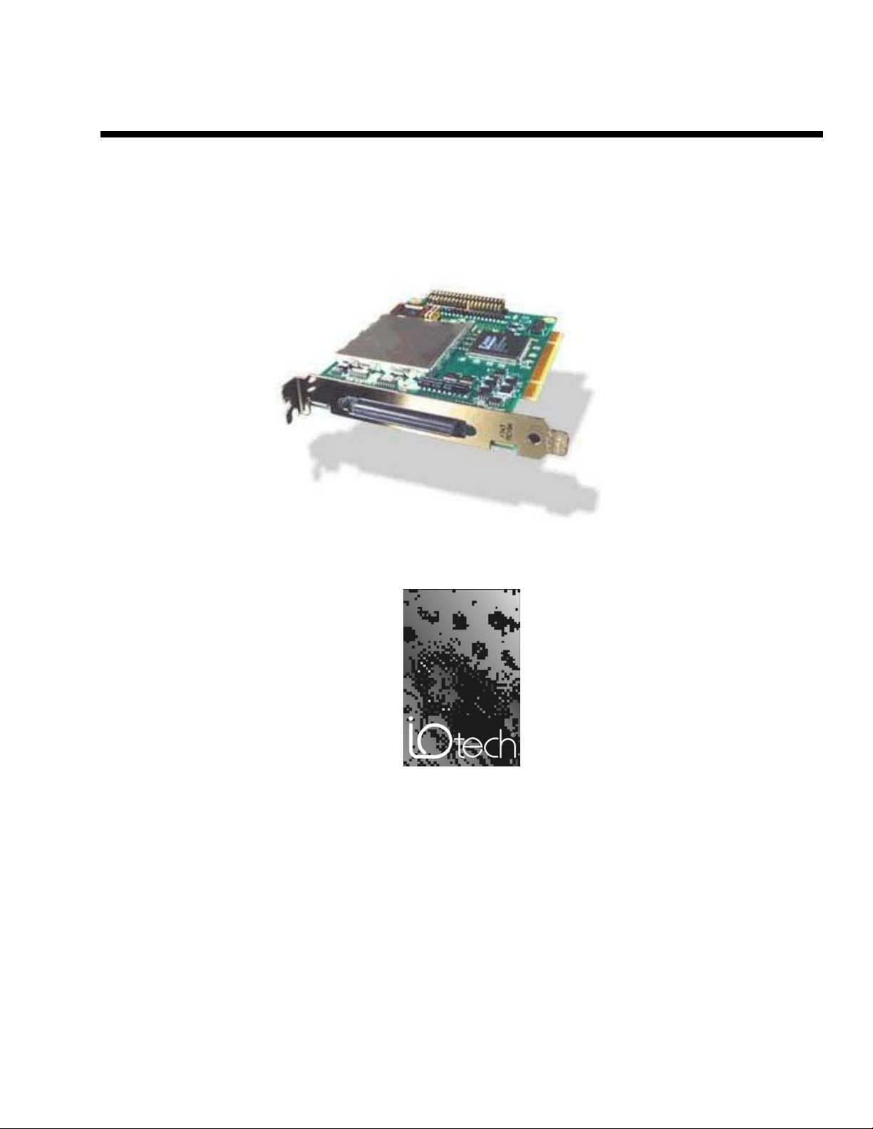
ADAC/5500 Series
PCI Data Acquisition Boards
Installation Guide
the smart approach to instrumentation ™
IOtech, Inc.
25971 Cannon Road
Cleveland, OH 44146-1833
Phone: (440) 439-4091
Fax: (440) 439-4093
E-mail (sales): sales@iotech.com
E-mail (post-sales): productsupport@iotech.com
Internet:
© 2002 by IOtech, Inc. 908096 1107-0940, rev. 2.0
www.iotech.com
Page 2
Warranty Information
Your IOtech warranty is as stated on the product warranty card. You may contact IOtech by phone,
fax machine, or e-mail in regard to warranty-related issues.
Phone: (440) 439-4091, fax: (440) 439-4093, e-mail: sales@iotech.com
Limitation of Liability
IOtech, Inc. cannot be held liable for any damages resulting from the use or misuse of this product.
Copyright, Trademark, and Licensing Notice
All IOtech documentation, software, and hardware are copyright with all rights reserved. No part of this product may be
copied, reproduced or transmitted by any mechanical, photographic, electronic, or other method without IOtech’s prior written
consent. IOtech product names are trademarked; other product names, as applicable, are trademarks of their respective
holders. All supplied IOtech software (including miscellaneous support files, drivers, and sample programs) may only be used
on one installation. You may make archival backup copies.
CE Notice
Many IOtech products carry the CE marker indicating they comply with the safety and emissions standards of the European
Community. As applicable, we ship these products with a Declaration of Conformity stating which specifications and operating
conditions apply.
Warnings, Cautions, Notes, and Tips
Refer all service to qualified personnel. This caution symbol warns of possible personal injury or equipment damage under
noted conditions. Follow all safety standards of professional practice and the recommendations in this manual. Using this
equipment in ways other than described in this manual can present serious safety hazards or cause equipment damage.
This warning symbol is used in this manual or on the equipment to warn of possible injury or death from electrical shock under
noted conditions.
This ESD caution symbol urges proper handling of equipment or components sensitive to damage from electrostatic discharge.
Proper handling guidelines include the use of grounded anti-static mats and wrist straps, ESD-protective bags and cartons, and
related procedures.
This symbol indicates the message is important, but is not of a Warning or Caution category. These notes can be of great
benefit to the user, and should be read.
In this manual, the book symbol always precedes the words “Reference Note.” This type of note identifies the location of
additional information that may prove helpful. References may be made to other chapters or other documentation.
Tips provide advice that may save time during a procedure, or help to clarify an issue. Tips may include additional reference.
Specifications and Calibration
Specifications are subject to change without notice. Significant changes will be addressed in an addendum or revision to the
manual. As applicable, IOtech calibrates its hardware to published specifications. Periodic hardware calibration is not
covered under the warranty and must be performed by qualified personnel as specified in this manual. Improper calibration
procedures may void the warranty.
Quality Notice
IOtech has maintained ISO 9001 certification since 1996. Prior to shipment, we thoroughly test our products and review our
documentation to assure the highest quality in all aspects. In a spirit of continuous improvement, IOtech welcomes your
suggestions.
During software installation, Adobe® PDF versions of user manuals are automatically installed onto your hard drive as a part of
product support. The default location is in the Programs group, which can be accessed from the Windows Desktop. A copy
of the Adobe Acrobat Reader® is included on your CD. The Reader provides a means of reading and printing the PDF
documents.
2 ADAC/5500 Series Installation Guide 908096 1107-0940, rev 2.0
Page 3
ADAC/5500 Series, Installation
Contents
Introduction …… page 3
Install Software …… page 5
Install Boards in Available
PCI Bus-Slots …… page 7
Configure Boards ….. page 9
Pinouts …… page 10
Introduction
This document is designed to help you quickly install your ADAC software and ADAC/5500 Series Board. More
detailed documents, in Adobe® PDF format, are installed on your hard-drive as a part of product support, during the
software installation process.
After installing the software and the board, you will need to configure the board. Although this document provides
some notes regarding board configuration, you will need to refer to your PDF copy of the ADAC/5500 Series User’s
Manual (p/n 1107-0905) for details.
You should keep your ADAC/5500 Series board’s serial number and your authorization code (if applicable) with
this document. Space is provided below for recording up to 4 board numbers and their PCI bus-slot location. The
board serial number is located on the bottom of the board
.
Board 1
Board 2
Board 3
Board 4
The host PC can support up to four ADAC/5500 Series Boards.
Board Type
(e.g., ADAC/5500MF,
ADAC/5503HR, etc.)*
Serial Number
PCI Bus-Slot Location
*Note: ADAC/5500 Series boards have device labels which read, for example, “ADAC/5500MF,”
“ADAC/5501MF,” etc. The name labels are convenient for users of more than one board type.
Authorization Code for purchased software (if applicable) ____________________________
If you purchased software that requires an authorization code, the code will be located on an
authorization code sheet that you will receive with your order.
WARNING
Always turn the computer power OFF and unplug it before connecting or disconnecting a screw
terminal panel or a cable to the PCI card. Failure to do so could result in electric shock, or
equipment damage.
Reference Notes:
(1) Each ADAC/5500 Series Board plugs into a PCI bus-slot. Consult your PC owner’s manual as needed.
(2) After the software install, you can navigate to relevant electronic documents from your desktop as follows:
Start ⇒ Programs ⇒ ADAC PDF Documentation
Accessing ADAC PDF Documentation
1107-0940, rev 2.0 908096 ADAC/5500 Series Installation Guide 3
Page 4
ADAC/5500 Series Boards
Feature
Analog Inputs
Ranges-
Unipolar
Bipolar
Resolution
A/D Sample
Rate
Gains
(Programmable)
D/A Outputs
(16-Bit)
Digital I/O
Counters
(16-Bit)
Timers
Associated
Terminal
Boards
Associated
Cables
(see figure)
/5500MF /5501MF
8 SingleEnded
0 to 10V 0 to10V
± 10V ± 10V
12-bit 12-bit 12-bit 16-bit 16-bit
100 kHz 100 kHz 100 kHz 200 kHz 200 kHz
N/A 1, 2, 4, 8 1, 10, 100, 1000 1, 2, 4, 8 1, 10, 100
0 2 Clocked DACs
16
(Two 8-bit
registers)
2 2 2 2 2
2 2 2 2 2
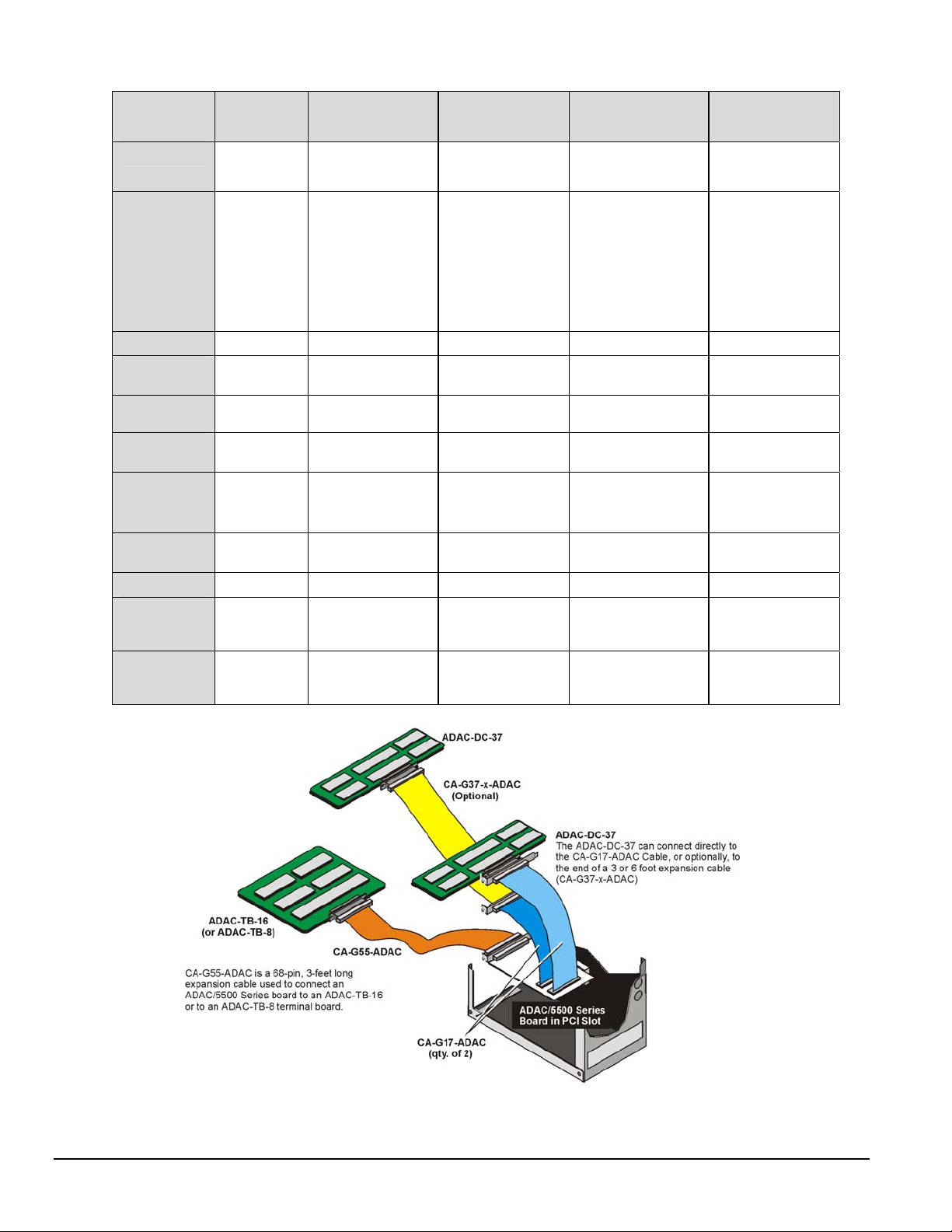
ADAC-TB-8 ADAC-TB-16
CA-G55ADAC
/5501MF-V
16 Single-Ended, or
16 Pseudo-Diff., or
8 Differential
0 to 5V
0 to 2.5V
0 to 1.25V
± 5V
± 2.5V
± 1.25V
(/5501MF-V only)
16 – from main I/O
(Two 8-bit registers)
16 – from aux. P3*
16 – from aux. P5*
ADAC-DC-37
CA-G55-ADAC
CA-G17-ADAC
CA-G37-x-ADAC
(qty. 2)
/5502MF
/5502MF-V
16 Single-Ended, or
16 Pseudo-Diff., or
8 Differential
0 to10V
0 to 1V
0 to 95mV
0 to 9.5mV
± 10V
± 1V
± 95mV
± 9.5mV
2 Clocked DACs
(/5502MF-V only)
16 – from main I/O
(Two 8-bit registers)
16 – from aux. P3*
16 – from aux. P5*
ADAC-TB-16
ADAC-DC-37 (qty. 2)
CA-G55-ADAC
CA-G17-ADAC
CA-G37-x-ADAC
/5503HR
/5503HR-V
16 Single-Ended, or
16 Pseudo-Diff., or
8 Differential
0 to10V
0 to 5V
0 to 2.5V
0 to 1.25V
± 10V
± 5V
± 2.5V
± 1.25V
2 Clocked DACs
(/5503HR-V only)
16 – from main I/O
(Two 8-bit registers)
16 – from aux. P3*
16 – from aux. P5*
ADAC-TB-16
ADAC-DC-37 (qty. 2)
CA-G55-ADAC
CA-G17-ADAC
CA-G37-x-ADAC
/5504HR
/5504HR-V
16 Single-Ended, or
16 Pseudo-Diff., or
8 Differential
0 to10V
0 to 1V
0 to 99.84 mV
± 10V
± 1V
± 99.86mV
2 Clocked DACs
(/5504HR-V only)
16 – from main I/O
(Two 8-bit registers)
16 – from aux. P3*
16 – from aux. P5*
ADAC-TB-16
ADAC-DC-37 (qty. 2)
CA-G55-ADAC
CA-G17-ADAC
CA-G37-x-ADAC
*
The CA-G17-ADAC cables connect to
40-pin headers P3 (DIO2) and P5 (DIO3)
located on ADAC Series board.
ADAC/5500 Series, Possible Connections to Terminal Boards
4 ADAC/5500 Series Installation Guide 908096 1107-0940, rev 2.0
Page 5

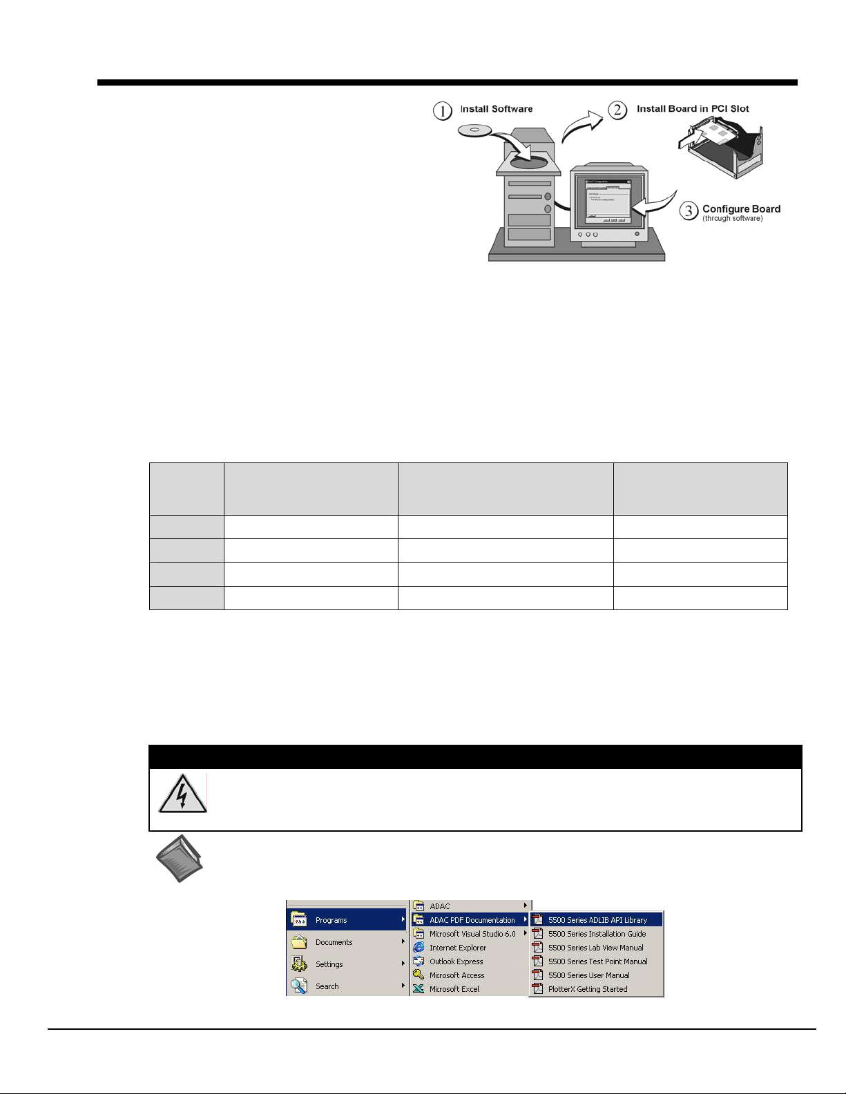
Step 1 – Install Software
IMPORTANT: Software must be installed before installing hardware.
Remove previous version ADAC drivers, if present. You can do this through Microsoft’s
1.
Add/Remove Programs feature.
2. Place the Data Acquisition CD into the CD-ROM drive. Wait for PC to auto-run the CD. This may
take a few moments, depending on your PC.
If the CD does not auto-run, use the Desktop’s Start/Run/Browse feature to select and run
Setup.exe.
3. After the intro-screen appears, follow the screen prompts.
Upon completing the software installation, continue with step 2, Install Boards in Available PCI Bus-Slots.
1107-0940, rev 2.0 908096 ADAC/5500 Series Installation Guide 5
Page 6

6 ADAC/5500 Series Installation Guide 908096 1107-0940, rev 2.0
Page 7

Step 2 – Install Boards in available PCI Bus-slots
IMPORTANT: Software must be installed before installing hardware.
WARNING
Turn OFF power to, and UNPLUG the host PC and externally connected equipment prior to
removing the PC’s cover and installing an ADAC/5500 Series Board. Failure to do so could
result in electric shock, or damage to equipment.
CAUTION
Take ESD precautions (packaging, proper handling, grounded wrist strap, etc.)
Use care to avoid touching board surfaces and onboard components. Only handle boards by their
edges (or ORBs, if applicable). Ensure boards do not come into contact with foreign elements such as
oils, water, and industrial particulate.
IMPORTANT: Bus Mastering DMA must be Enabled.
For an ADAC/5500 Series board to operate properly, Bus Mastering DMA must be enabled on
the PCI slot [for which the board is to be installed]. Prior to installation, verify that your
computer is capable of performing Bus Mastering DMA for the applicable PCI slot. Note that
some computers have BIOS settings that enable [or disable] Bus Mastering DMA. If your
computer has this BIOS option, ensure that Bus Mastering DMA is Enabled on the appropriate
PCI slot.
Refer to your PC Owner's Manual for additional information regarding your PC and enabling
Bus Mastering DMA for PCI slots.
1. Turn OFF power to, and UNPLUG the host PC and externally connected equipment.
2. Remove the PC’s cover. Refer to your PC Owner’s Manual as needed.
3. Choose an available PCI bus-slot.
4. Carefully remove ADAC/5500 Series Board from its anti-static protective bag. If you have not already done so,
write down the serial number and type of ADAC board in the space provided on page 3 of this document.
5. On the PC’s rear panel, loosen and remove the screw for the blank adapter plate that corresponds with the chosen
PCI bus. See left-hand figure, below.
Removing a Blank Adapter Plate
Installing an ADAC/5500 Series Board
6. Remove the blank adapter plate. Refer to your PC Owner’s Manual if needed.
1107-0940, rev 2.0 908096 ADAC/5500 Series Installation Guide 7
Page 8

7. Align the groove in the ADAC/5500 Series board’s PCI edge-connector with the ridge of the desired PCI slot.
See preceding right-hand figure.
8. Push the board firmly into the PCI slot. The board should “snap” into position.
9. Secure the board by inserting the rear-panel adapter-plate screw.
10. Using the previous steps, install additional boards into available PCI bus-slots, if applicable to your application.
11. Replace the computer’s cover.
12. Plug in all cords and cables that were removed in step 1.
13. Apply power to, and start up the PC.
Note: At this point some PCs may prompt you to insert an installation disk. While this is rare, if you do receive
such a prompt simply place the install CD-ROM into the disk drive and follow additional screen prompts.
Reference Notes:
After you have completed the installation you should refer to the electronic documents that were
automatically installed onto your hard drive as a part of product support. The default location is in the
Programs group, which can be accessed from the Windows Desktop.
ADAC related documents, in Adobe® PDF format, are:
É
ADAC/5500 Series User’s Manual, p/n 1107-0905
(ADAC5500 Series Users Manual.pdf)
É
ADAC-LVi User’s Manual, Data Acquisition VIs for LabView, p/n 1107-0901
(ADAC-LVi Users Manual.pdf)
É
ADLIB WIN Interface Library Software User’s Manual, p/n 1107-0902
(ADLIB WIN Users Manual.pdf)
É
TP ADAC-32 (32-Bit TestPoint Driver) User’s Manual, p/n 1107-0903
(TP ADAC-32 Users Manual.pdf)
É
PlotterX, PlotterX Plus, and ADAC Config Getting Started, p/n 1107-0941
(PlotterX-GettingStarted.pdf)
8 ADAC/5500 Series Installation Guide 908096 1107-0940, rev 2.0
Page 9

Step 3 – Configure Boards
Always turn the computer power OFF and unplug it before connecting or disconnecting a screw
terminal panel or a cable to the PCI card. Failure to do so could result in electric shock, or
damage to equipment.
Before you can use your ADAC/5500 Series Board, you will need to configure it using the ADAC/5500 Series
User’s Manual, p/n 1107-0905 (ADAC5500 Series Users Manual.pdf) for reference. However, prior to doing so
you may find it helpful to review the following points:
All configurations, including data-acquisition settings such as analog input, data collection rates, input
•
voltage range, and operating modes are made through ADAC configuration software. The ADAC
configuration software (ADAC Config) file can be accessed from the Windows desktop Start Menu by
navigating as follows:
WARNING
Start ⇒ Programs ⇒ ADAC ⇒ ADAC Config ⇒ ADAC Config
Desktop Path to ADAC Config
ADAC ADLIB WDM software drivers provide an application level software interface to Windows
•
98/ME/NT/2000/XP. Software packages such as LabVIEW™ communicate through our ADLIB
driver software. These packages configure and collect, or output, acquisition data in a GUI based
interface.
•
The ADAC/5501MF, ADAC/5502MF, ADAC/5503HR and ADAC/5504HR analog inputs are
impedance buffered and drive a differential gain amplifier that can be referenced in a number of ways,
allowing the following programmable input configurations: Single-Ended, Pseudo-Differential, and
Fully-Differential.
•
The ADAC/5500MF analog inputs are impedance buffered. They can only be referenced in Single-
Ended input configuration. 1 to 176 element channel-configuration RAM is provided to allow each
ADC channel to be programmed with a different combination of Gain, Range, and Input Configuration.
Note that these modes also apply to expansion channels located on the ADAC line of accessory screw
terminal panels.
•
The analog inputs on the ADAC/5500, ADAC/5501MF, ADAC/5502MF, ADAC/5503HR and
ADAC/5504HR may be configured for either ±10 V bipolar or 0-10 V unipolar operation. The input
range is programmable on a channel-by-channel basis in a 176-element channel configuration RAM.
Note that the range selection also applies to expansion channels.
•
The programmable gain circuitry on the ADAC/5501MF, ADAC/5502MF, ADAC/5503HR and
ADAC/5504HR must be taken into account in defining the usable error free input range. The boards
provide a wide range of programmable ranges and resolutions.
•
The ADAC/5500 Series Boards each bring out ±15 V and +5 V to the main I/O connector (J1). In
addition, the ADAC/5501MF, ADAC/5502MF, ADAC/5503HR and ADAC/5504HR bring +5 V to the
auxiliary digital I/O connectors (P3 and P5), located on the backside of those boards. These power lines
are individually fused to protect the ADAC/5500 Series Board. Note that connecting or disconnecting
cables or screw terminal panels (as well as any user connections to these power lines) may blow a fuse,
or cause damage to the board.
•
Incorrect connection of user wiring is one of the most common problems experienced by users of data
acquisition boards. To ensure proper results, you must first determine what type of signal source you are
measuring (Ground Referenced Source or Floating Source), and then choose the appropriate input
configuration on your data acquisition card (Differential, Pseudo-Differential, or Single-Ended). Your
user’s manual provides detailed information.
1107-0940, rev 2.0 908096 ADAC/5500 Series Installation Guide 9
Page 10

Pinouts
(
)
This section contains pinouts for the various ADAC/5500 Series Boards and the terminal boards that can be used
with them, i.e., ADAC-TB-8, ADAC-TB-16, and DC-37.
J1 Pin Assignments for ADAC/5500MF Only
Standard 68-Pin SCSCI Type III, Socket (Female) Connector with Orb
Pin
Signal Description /
Comments
1 DGND Digital Ground 35 +5 V (fused) Power
2 +15 V (fused) Power 36 +5 V
3 -15 V (fused) Power 37 +5 V (fused) Power
4 ADTGOUT / TMR0 Internal ADC Trigger Output
5 ADCLKOUT / TMR1 Internal ADC Trigger Output
6 N/C Not Connected 40 CNTR1 Counter 1 Clock Input
7 DIO_15 TTL Level Digital I/O Ch. 15 41 DIO_14 TTL Level Digital I/O Ch. 14
8 DIO_13 TTL Level Digital I/O Ch. 13 42 DIO_12 TTL Level Digital I/O Ch. 12
9 DIO_11 TTL Level Digital I/O Ch. 11 43 DIO_10 TTL Level Digital I/O Ch. 10
10 DIO_9 TTL Level Digital I/O Ch. 9 44 DIO_8 TTL Level Digital I/O Ch. 8
11 DIO_7 TTL Level Digital I/O Ch. 7 45 DIO_6 TTL Level Digital I/O Ch. 6
12 DIO_5 TTL Level Digital I/O Ch. 5 46 DIO_4 TTL Level Digital I/O Ch. 4
13 DIO_3 TTL Level Digital I/O Ch. 3 47 DIO_2 TTL Level Digital I/O Ch. 2
14 DIO_1 TTL Level Digital I/O Ch. 1 48 DIO_0 TTL Level Digital I/O Ch. 0
15 DGND Digital Ground 49 N/C Not Connected
16 N/C Not Connected 50 N/C Not Connected
17 N/C Not Connected 51 N/C Not Connected
18 N/C Not Connected 52 N/C Not Connected
19 N/C Not Connected 53 N/C Not Connected
20 N/C Not Connected 54 N/C Not Connected
21 AGND Analog Ground 55 AGND Analog Ground
22 N/C Not Connected 56 N/C Not Connected
23 SGND Signal Ground 57 N/C Not Connected
24 N/C Not Connected 58 N/C Not Connected
25 AIN_7 Analog Input, Ch. 7 59 AIN_3 Analog Input, Ch. 3
26 N/C Not Connected 60 N/C Not Connected
27 AIN_6 Analog Input, Ch. 6 61 AIN_2 Analog Input, Ch. 2
28 N/C Not Connected 62 N/C Not Connected
29 AIN_5 Analog Input, Ch. 5 63 AIN_1 Analog Input, Ch. 1
30 N/C Not Connected 64 N/C Not Connected
31 AIN_4 Analog Input, Ch. 4 65 AIN_0 Analog Input, Ch. 0
32 N/C Not Connected 66 N/C Not Connected
33 N/C Not Connected 67 N/C Not Connected
34 AGND Analog Ground 68 DGND Digital Ground
/ Timer 0 Clock Output
/ Timer 1 Clock Output
Pi
n
38 ADTGIN External Gate (level controlled),
39 ADCLKIN / CNTR0 External ADC Clock In, or
Signal
fused
Description / Comments
Power
or External Trigger (edge active)
Counter 0. Rising or Falling
Edge Sensitive.
10 ADAC/5500 Series Installation Guide 908096 1107-0940, rev 2.0
Page 11

(
)
J1 Pin Assignments for ADAC/5501MF, ADAC/5502MF, ADAC/5503HR, and ADAC/5504HR
Standard 68-Pin SCSCI Type III, Socket (Female) Connector with Orb
Pin
1 DGND Digital Ground 35 +5 V (fused) Power
2 +15 V (fused) Power 36 +5 V
3 -15 V (fused) Power 37 +5 V (fused) Power
4 ADTGOUT / TMR0 Internal ADC Trigger Output /
5 ADCLKOUT /
6 DATRIGIN DAC0 External Gate (Level
7 DIO_15 TTL Level Digital I/O Ch. 15 41 DIO_14 TTL Level Digital I/O Ch. 14
8 DIO_13 TTL Level Digital I/O Ch. 13 42 DIO_12 TTL Level Digital I/O Ch. 12
9 DIO_11 TTL Level Digital I/O Ch. 11 43 DIO_10 TTL Level Digital I/O Ch. 10
10 DIO_9 TTL Level Digital I/O Ch. 9 44 DIO_8 TTL Level Digital I/O Ch. 8
11 DIO_7 TTL Level Digital I/O Ch. 7 45 DIO_6 TTL Level Digital I/O Ch. 6
12 DIO_5 TTL Level Digital I/O Ch. 5 46 DIO_4 TTL Level Digital I/O Ch. 4
13 DIO_3 TTL Level Digital I/O Ch. 3 47 DIO_2 TTL Level Digital I/O Ch. 2
14 DIO_1 TTL Level Digital I/O Ch. 1 48 DIO_0 TTL Level Digital I/O Ch. 0
15 DGND Digital Ground 49 CJ2 Reserved
16 CJ1 Reserved 50 CJ0 Reserved
17 MUX7 Reserved 51 MUX6 Reserved
18 MUX5 Reserved 52 MUX4 Reserved
19 MUX3 Reserved 53 MUX2 Reserved
20 MUX1 Reserved 54 MUX0 Reserved
21 AGND Analog Ground 55 AGND Analog Ground
22 ADEX_LO Reserved, AD Expansion LO 56 ADEX_HI Reserved, AD Expansion HI
23 SGND Signal Ground 57 PDIN Pseudo-Differential Input return
24 AIN_15 Analog Input, Ch. 15 58 AIN_7 Analog Input, Ch. 7
25 AIN_14 Analog Input, Ch. 14 59 AIN_6 Analog Input, Ch. 6
26 AIN_13 Analog Input, Ch. 13 60 AIN_5 Analog Input, Ch. 5
27 AIN_12 Analog Input, Ch. 12 61 AIN_4 Analog Input, Ch. 4
28 AIN_11 Analog Input, Ch. 11 62 AIN_3 Analog Input, Ch. 3
29 AIN_10 Analog Input, Ch. 10 63 AIN_2 Analog Input, Ch. 2
30 AIN_9 Analog Input, Ch. 9 64 AIN_1 Analog Input, Ch. 1
31 AIN_8 Analog Input, Ch. 8 65 AIN_0 Analog Input, Ch. 0
32 RTN1 Voltage output return, line 1. 66 DAC1 (Note 2) Digital-to-Analog Converter 1
33 RTN0 Voltage output return, line 0. 67 DAC0 (Note 1) Digital-to-Analog Converter 0
34 AGND Analog Ground 68 DGND Digital Ground
Signal Description / Comments
Timer 0 Clock Output
TMR1
Internal ADC Trigger Output /
Timer 1 Clock Output
Controlled), or External
Trigger ( Edge Active)
Pi
n
38 ADTGIN External Gate (level controlled),
39 ADCLKIN / CNTR0 External ADC Clock In, or
40 DACLKIN / CNTR1 External ADC Clock In, or
Signal
fused
Description / Comments
Power
or External Trigger (edge active)
Counter 0. Rising or Falling Edge
Sensitive.
Counter 0. Rising or Falling Edge
Sensitive.
Note 1: The clock source of the primary DAC0 channel may be software command, DAC0 Pacer clock,
or an external event (DACLKIN).
Note 2: The clock source of the secondary DAC1 channel may be software command, DAC1 Pacer clock,
or Channel 0 clock source.
1107-0940, rev 2.0 908096 ADAC/5500 Series Installation Guide 11
Page 12

P3 and P5 Pin Assignments
The ADAC/5501MF, ADAC/5502MF, ADAC/5503HR and ADAC/5504HR include two auxiliary 40-pin headers. These
are located on the back of the boards, and provide access to the two 16-bit DIO ports (DIO2 and DIO3). Two CA-G17ADAC cables can be used to bring the DIO2 and DIO3 headers to separate37-pin D-type connectors [one GA-17 cable per
DIO header]. GA17’s orb (following figure) mounts at the back of the host PC.
The DB37-end of a CA-G17-ADAC Cable, which includes an Orb for PC Mounting
SIGNAL NAME P3 PIN or
P5 PIN
DGND 1 1 DGND 21 11
+ 5 V (fused) 2 20 D9 22 30
DGND 3 2 DGND 23 12
D0 4 21 D10 24 31
DGND 5 3 DGND 25 13
D1 6 22 D11 26 32
DGND 7 4 DGND 27 14
D2 8 23 D12 28 33
DGND 9 5 DGND 29 15
D3 10 24 D13 30 34
DGND 11 6 DGND 31 16
D4 12 25 D14 32 35
DGND 13 7 DGND 33 17
D5 14 26 D15 34 36
DGND 15 8 DGND 35 18
D6 16 27 STROBE2 / 3 36 37
DGND 17 9 DGND 37 19
D7 18 28 DGND 38 n/c
DGND 19 10 DGND 39 n/c
D8 20 29 DGND 40 n/c
G17 PIN
(37-pin D)
SIGNAL NAME P3 PIN or
P5 PIN
G17 PIN
(37-pin D)
P3 & P5 Auxiliary Digital I/O Connectors
Standard 40-Pin Male Headers
A CA-G17-ADAC Cable, Installed
Signal definitions for the P3 and P5 Auxiliary 40-Pin DIO headers and the DB37 connector follow.
12 ADAC/5500 Series Installation Guide 908096 1107-0940, rev 2.0
Page 13

Signal Definitions for P3, P5, and GB17’s DB37 Connector
The following descriptions apply to each of the signals that are available at the 40-pin auxiliary DIO headers,
designated as P3 and P5. The headers are located on the back of boards: ADAC/5501MF, ADAC/5502MF,
ADAC/5503HR, and ADAC/5504HR. In addition, the signals apply to the corresponding pins on GA17’s DB37
connector as indicated in the table on the preceding page.
GA17’s orb (following figure) mounts at the back of the host PC.
The DB37-end of a CA-G17-ADAC Cable, which includes an Orb for PC Mounting
D0... D15 These signals are the sixteen 5 V CMOS/LSTTL level digital input/output lines of DIO2 on
connector P3, and the D103 connector on P5.
On G17’s DB37 connector, D0 through D15 correspond to pins 21 through 36, with DB0
assigned to pin 21, DB1 assigned to pin 22, DB2 assigned to pin 23, etc.
DGND This signal is the +5 V power return line. It may also be used as a reference ground for TTL
signals. On G17’s DB37 connector, the DGND lines connect to pins 1 through 19, inclusive.
+5 V This signal is +5 V power voltage signal that is sourced directly from the PC bus. The +5 V lines
are fused at 3 amps. See WARNING. On G17’s DB37 connector, the +5 V power signal
corresponds to pin 20.
WARNING
Possible electric shock. Take great care when using the +5 V power as the voltage signal is
sourced directly from the PC Bus. The +5 V lines are fused at 3 Amps.
STROBE The Strobe2 signal is provided on the DIO2 37-pin interface and the Strobe3 signal is provided on
the DIO3 interface. When either port is configured as an input port, the associated Strobe signal is
disabled and placed in a High Impedance state (Z off). When DIO port is configured as an output
port, the associated strobe signal will be pulsed low for 1 microsecond following each data output
event that occurs.
On system power-up the DIO Strobe signals are disabled and placed in a High Impedance state
(Z off). 3.3 V CMOS signal.
In regard to the G17 DB37 connector, pin-37 is used for the strobe signal.
1107-0940, rev 2.0 908096 ADAC/5500 Series Installation Guide 13
Page 14

ADAC-TB-8 Screw-Terminal Board Connections
The ADAC-TB-8 provides screw-terminal access to all of a ADAC/5500MF board’s analog and digital I/O
signals. The terminal board connects to the ADAC/5500MF via a 3-foot long 68-pin conductor expansion
cable, p/n CA-G55-ADAC. The terminal board accepts wire up to 14 AWG.
ADAC-TB-8
WARNING
Always turn the computer power OFF and unplug it before connecting or disconnecting a screw
terminal panel or a cable to the PCI card. Failure to do so could result in electric shock, or
equipment damage.
14 ADAC/5500 Series Installation Guide 908096 1107-0940, rev 2.0
Page 15

ADAC-TB-16 Screw-Terminal Board
One ADAC-TB-16 provides screw-terminal access to all analog and digital I/O signals from any one of the
following boards: ADAC/5501MF, ADAC/5501MF-V, ADAC/5503HR, and ADAC/5503HR-V. The
terminal board connects to the board via a 3-foot long 68-pin conductor expansion cable, p/n CA-G55ADAC. The terminal board accepts wire up to 14 AWG.
ADAC-TB-16
WARNING
Always turn the computer power OFF and unplug it before connecting or disconnecting a screw
terminal panel or a cable to the PCI card. Failure to do so could result in electric shock, or
equipment damage.
1107-0940, rev 2.0 908096 ADAC/5500 Series Installation Guide 15
Page 16

ADAC-DC-37 Screw-Terminal Board for Auxiliary Digital I/O
The ADAC-DC-37 provides access to 16 of the 32 available auxiliary digital I/O channels from
ADAC/5501MF, ADAC/5501MF-V, ADAC/5503HR, and ADAC/5503HR-V boards. Two ADAC-DC37 terminal boards are required to access all 32 digital I/O channels.
As depicted on page 4, each DC-37 terminal board can connect to an ADAC/5500 Series Board via a
CA-G17-ADAC cable, or to an optional CA-G37-x-ADAC extension cable, which interfaces between a
CA-G17 cable’s orb and the ADAC-DC-37 board.
ADAC-DC-37
WARNING
Always turn the computer power OFF and unplug it before connecting or disconnecting a screw
terminal panel or a cable to the PCI card. Failure to do so could result in electric shock, or
equipment damage.
16 ADAC/5500 Series Installation Guide 908096 1107-0940, rev 2.0
 Loading...