


The MicroControllerShop
http://microcontrollershop.com
PIC-P40-28
Prototyping Board
User Manual
Rev. 1.0
February 2008

The MicroControllerShop
MicroController Pros Corporation
http://microcontrollershop.com
Table of Contents
1.0 Preface ................................................................................................................................................... 3
1.1. Cautions............................................................................................................................................. 3
1.2. Trademarks........................................................................................................................................ 3
1.3. Limited Guarantee and Support ........................................................................................................ 3
1.4. Copyright ........................................................................................................................................... 3
2.0 Introduction............................................................................................................................................. 4
3.0 Hardware ................................................................................................................................................ 5
3.1. PIC-P40-28 Board Components........................................................................................................ 5
3.2. Power Supply Requirements ............................................................................................................. 6
3.3. 14- and 18-pin MCU sockets ............................................................................................................. 6
3.4. MCU Oscillator Circuit ....................................................................................................................... 7
3.5. In-Circuit Serial Programming (ICSP) and In-Circuit Debug (ICD) Interface..................................... 7
3.6. RS232 Interface................................................................................................................................. 9
3.7. Reset Circuit .................................................................................................................................... 11
3.8. LED.................................................................................................................................................. 11
3.9. Push Button ..................................................................................................................................... 11
3.10. Board Dimensions & PCB Material................................................................................................ 11
Appendix A. Board Schematic.................................................................................................................... 12
PIC-P40-28 User Manual February 2008

The MicroControllerShop
MicroController Pros Corporation
http://microcontrollershop.com
1.0 Preface
1.1. Cautions
Caution: Check power supply requirements. Incorrect voltage will damage the board. See chapter 3.2
for details.
Caution: Only populate one socket at a time. Do not insert microcontrollers into more than one socket
at a time, or you may damage the microcontroller chips.
Caution: Check the pin orientation of the sockets before inserting a chip. The 28- pin socket is
rotated by 180 degrees in relation to the 40-pin socket (see ). This means that the pin 1
location for the 28-pin socket is in the lower right hand corner, whereas the pin 1 position for the 40-pin
socket is in the upper left hand corner of the socket. Make sure you align pin 1 of your microcontroller
with pin 1 of the socket. Inserting a microcontroller chip incorrectly can damage it.
1.2. Trademarks
Figure 3-1
All brand or product names used in this manual are trademarks or registered trademarks of their
respective companies or organizations.
1.3. Limited Guarantee and Support
MicroController Pros Corp. warrants the PIC-P40-28 board to be free from component or assembly
defects for a period of 180 days from the date of purchase. Settlement is limited to repair or replacement
of the product only. MicroController Pros Corp. does not assume any liability arising out of the application
or use of any product, circuit or procedure described herein. No other liability or warranty applies,
expressed or implied. While every attempt has been made to ensure accurate documentation,
MicroController Pros Corp. cannot be held responsible for errors or omissions, and reserves the right to
make changes without prior notice.
This prototype board is intended as a low-cost development tool with limited support. It is assumed that
you are familiar with basic electrical engineering concepts and microcontroller code development. Our
support does not include us teaching you those concepts. If you experience functional issues with this
board, you can contact support via email: support@microcontrollershop.com
General information on Microchip PIC microcontrollers can be found at the following URL:
http://www.microchip.com
1.4. Copyright
© 2008 MicroController Pros Corporation. All rights reserved.
Website: http://microcontrollershop.com
PIC-P40-28 User Manual 3/ 12 February 2008

The MicroControllerShop
MicroController Pros Corporation
http://microcontrollershop.com
2.0 Introduction
The PIC-P40-28 is a prototype board for Microchip PIC microcontrollers in a 28- or 40-pin DIP package.
Check the pinout of the PIC microcontroller, which you intent to use with this board, in the Microchip PIC
device datasheet. Verify that the PIC’s Vdd, Vss, OSC1, OSC2, ICSP programming, and UART Rx and
Tx signals match the location of those pins on the appropriate MCU socket of this board (see schematic).
The board comes completely assembled and tested and offers the following features:
• 28-pin, and 40-pin DIL microcontroller sockets
• Jumper selectable +3.3V or +5.0V board supply voltage
• Power plug-in jack: 5.5mm outer, 2.5mm inner diameter
o Accepts AC and DC input voltage
• RS232 DB9 female connector with MAX2232 interface circuit and Tx, Rx, CTS and DTR/RTS
signals. Rx and Tx signals are routed to 28-pin and 40-pin MCU sockets (see schematics).
• RJ12 and 6-pin, single row In-Circuit Serial Programming (ICSP) connectors for in-circuit
programming and debugging with a PIC In-Circuit Debugger & Programmer.
• 20 MHz quartz crystal oscillator in machined, spring-loaded socket for easy oscillator replacement
• Reset button
• Push button connected to PIC I/O pin via removable jumper
• Status LED connected to PIC I/O pin via removable jumper
• Extension solder pads for every µC pin
• Prototyping area with 100 mils grid
• Prototyping GND bus
• Prototyping Vcc bus
• FR-4, 1.5 mm (0.062″), single layer, electroless nickel/immersion gold (ENIG) plating, green
soldermask, white silkscreen component print
• Four mounting holes
PIC-P40-28 User Manual 4/ 12 February 2008
MicroController Pros Corporation
Socketed 20MHz Crystal
ge
L
D
ct
M
T
3.0 Hardware
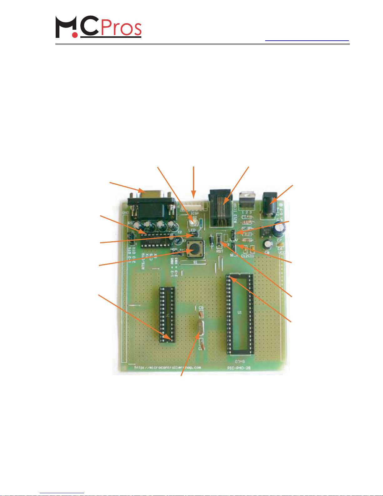
3.1. PIC-P40-28 Board Components
Figure 3-1
shows the PIC-P40-28 Board with major components identified.
The MicroControllerShop
http://microcontrollershop.com
6-pin, single row
LED
RS232 Interface
(D-Sub 9 female)
AX2232 RS232
ransceiver
ED Connect/
isconnect Jumper
Push Button
S1
Pin 1 of
28-pin socket
ICSP/ICD Connector
RJ12 Jack
ICSP/ICD Connector
Power Connector
Board Supply Volta
Selection Jumper
Open: 5.0V
Closed: 3.3V
Push Button
Connect/Disconne
Jumper
Reset Button
Pin1 of
40-pin socket
S1
PIC-P40-28 User Manual 5/ 12 February 2008
Figure 3-1: PIC-P40-28 Board

The MicroControllerShop
MicroController Pros Corporation
3.2. Power Supply Requirements
Power input to the board is supplied via a barrel connector with 5.5mm outer and 2.5mm inner diameter.
An on-board bridge rectifier provides polarity reversal protection and allows you to use both AC or DC
input voltages.
An on-board LM317 adjustable output voltage regulator can be set via a jumper to provide the board with
either 5.0V or 3.3V DC operating voltage. In the open position of jumper 3.3V, the output voltage is 5.0V.
In the jumper-closed position, the output voltage is 3.3V
Jumper 3.3V Board Operating Voltage (BOV)
Open 5.0V DC
Closed 3.3V DC
The input voltage supplied to the board should be at least 3.5V above the desired board operating voltage
(BOV) if you use a DC power supply, and 2.5V above BOV if you use an AC power supply.
Minimum AC input voltage
Minimum DC input voltage
The following maximum input voltages should not be exceeded by your power supply, otherwise you risk
damaging the board:
Maximum AC input voltage
Maximum DC input voltage
The current rating of your power supply is uncritical, as this board requires less than 100mA to operate.
Therefore, any power supply with a current rating of 100mA or higher can be used. A higher current rating
is not a problem, as the board will only draw as much current from the supply as is needed for operation.
In general, you should use voltages close to the minimum required input voltage. It reduces stress on the
voltage regulator, as a smaller voltage differential has to be dissipated into heat.
A word of caution, however: Many cheap transformer-based wall-plug power supplies provide an
unregulated output voltage that under no load is usually much higher than the rated output voltage printed
on the supply. This high output voltage then “collapses” under load and can be lower than the rated
output voltage. To avoid damage to your board, verify with a multi-meter that the true voltage of your
power supply is within the above stated limits before connecting it to this board.
5.0V Board Operating Voltage 3.3V Board Operation Voltage
7.5V AC 5.8V AC
8.5V DC 6.8V DC
10.5V AC
15V DC
http://microcontrollershop.com
3.3. 28- and 40-pin MCU sockets
Caution: Only populate one socket at a time. Do not insert microcontrollers into more than one socket
at a time, or you may damage the microcontroller chips.
Caution: Check the pin orientation of the sockets before inserting a chip. The 28- pin socket is
rotated by 180 degrees in relation to the 40-pin socket (see ). This means that the pin 1
location for the 28-pin socket is in the lower right hand corner, whereas the pin 1 position for the 40-pin
socket is in the upper left hand corner of the socket. Make sure you align pin 1 of your microcontroller
with pin 1 of the socket. Inserting a microcontroller chip incorrectly can damage it.
PIC-P40-28 User Manual 6/ 12 February 2008
Figure 3-1

The MicroControllerShop
MicroController Pros Corporation
Check the pinout of the PIC microcontroller, which you intent to use with this board, in the Microchip PIC
device datasheet. Verify that the PIC’s Vdd, Vss, OSC1, OSC2, ICSP programming, and UART Rx and
TX signals match the location of those pins on the appropriate MCU socket of this board (see schematic).
The board has routed connections from both sockets to the RS232 Rx and Tx pins, ICSP signals, a push
button, a reset button, an LED and a crystal oscillator.
Each unused MCU pin has a direct connection to the solder pad next to it. You can solder square header
pins into those locations and then use prototyping jumper wires to connect to other circuitry. Alternatively,
you can directly solder wire connections or component pins to these pads. Using header pins and jumper
wires gives you the flexibility to connect the MCU pins to different components on the board quickly.
For header pins, see: http://microcontrollershop.com/product_info.php?products_id=2115
For prototyping jumper wires, see: http://microcontrollershop.com/product_info.php?products_id=791
3.4. MCU Oscillator Circuit
A 20MHz crystal oscillator is connected to the 28-pin and 40-pin socket oscillator pins. The crystal is
socketed, so you can easily replace it with a different frequency value.
http://microcontrollershop.com
Figure 3-2: Socketed Crystal
3.5. In-Circuit Serial Programming (ICSP) and In-Circuit Debug (ICD) Interface
PIC microcontrollers use the same connection for in-circuit serial programming (ICSP) and in-circuit
debugging (ICD). Figure 3-1 shows the location of the ICSP/ICD connectors. The board features two
ICSP/ICD connectors - an RJ12 jack and a 6-pin single row, latched header - to provide compatibility with
a broad selection of PIC programmers and in-circuit debuggers. The ICSP signals are routed to the
appropriate pins of both PIC MCU sockets.
PIC-P40-28 User Manual 7/ 12 February 2008
The MicroControllerShop
1
2
3
4 5
6
MicroController Pros Corporation
Some 40-pin PIC microcontrollers have the optional PGM programming signal on pin 38 (RB5), others on
pin 25 (RB3). If you use a programmer that requires the PGM signal, make sure you connect it to the
correct MCU pin, by setting jumper PGM_sel according to the table below.
PGM_sel
position
40-pin PIC Socket Pin
# (Name)
1-2 PGM_RB5 38 (RB5)
2-3 PGM_RB3 36 (RB3)
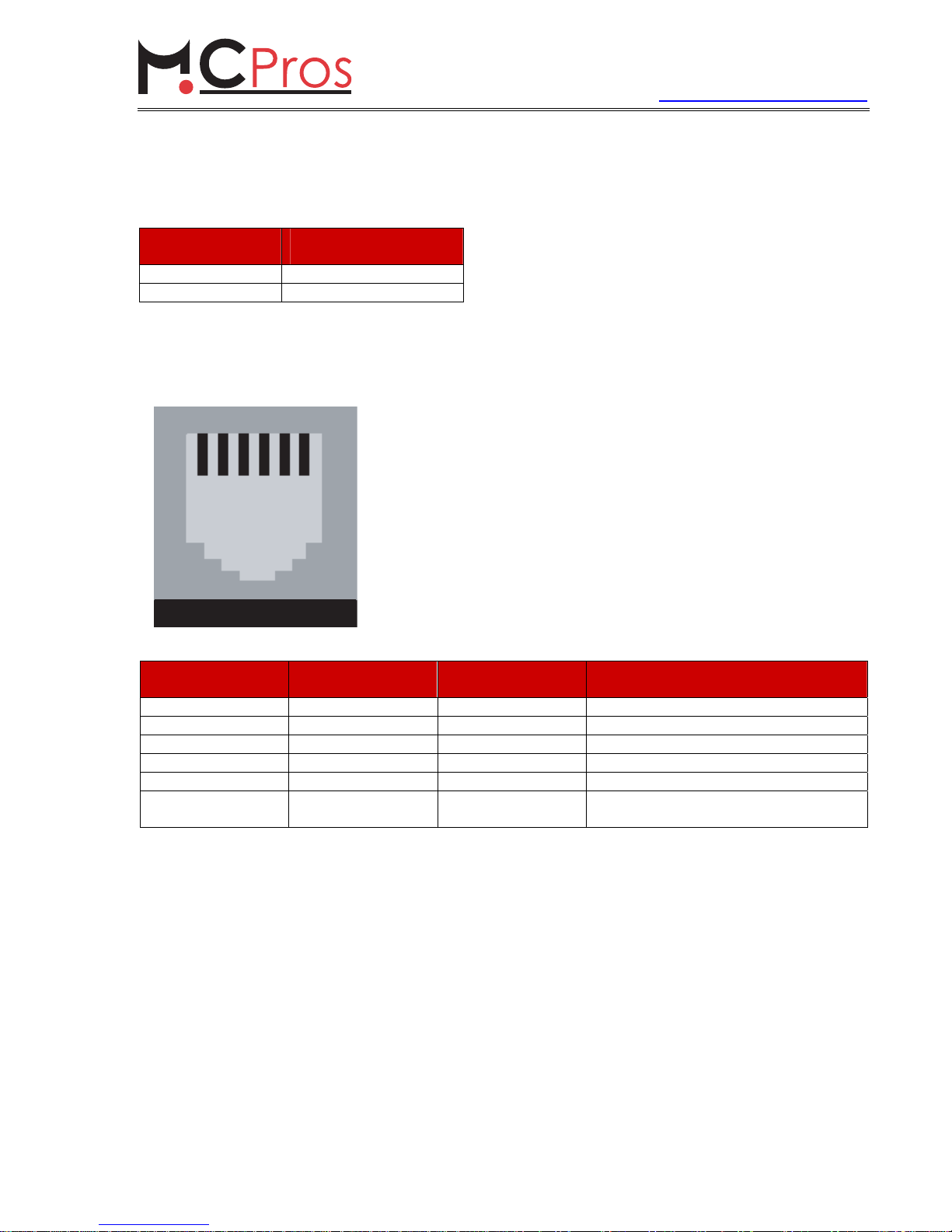
The board’s RJ12 ICSP/ICD jack is connected as shown in the figure and table below.
http://microcontrollershop.com
1
Figure 3-3: RJ12 PIC ICSP Connector
Signal Name Board ICSP/ICD
Connector Pin
28-pin PIC Socket
Pin
40-pin PIC Socket Pin
/MCLR 1 1 1
Vdd (Vcc) 2 20 11 & 32
Vss (GND) 3 8 & 19 12 & 31
PGD 4 28 40
PGC 5 27 39
PGM (optional) 6 24 36 or 38 (depending on PGM_sel
Jumper position)
PIC-P40-28 User Manual 8/ 12 February 2008

The MicroControllerShop
C
D
D
d
r
LR
MicroController Pros Corporation
The board’s 6-pin, single row ICSP/ICD header is connected as shown in the figure and table below.
http://microcontrollershop.com
6
5
4
3
2
1
Signal Name Board ICSP/ICD
/MCLR 1 1 1
Vdd (Vcc) 2 20 11 & 32
Vss (GND) 3 8 & 19 12 & 31
PGD 4 28 40
PGC 5 27 39
PGM (optional) 6 24 36 or 38 (depending on PGM_sel
For compatible PIC ICSP programmers, see:
http://microcontrollershop.com/default.php?cPath=112_97
For compatible PIC ICD in-circuit debuggers & programmers, see:
http://microcontrollershop.com/default.php?cPath=112_152
PGM
PG
PG
GN
Vd
/MC
Figure 3-4: 6-pin, Single Row, PIC ICSP
Connecto
Connector Pin
with Latch and 0.1” Spacing
28-pin PIC Socket
Pin
40-pin PIC Socket Pin
Jumper position)
3.6. RS232 Interface
RS232 devices are classified as Data Terminal Equipment (DTE) or Data Communications Equipment
(DCE). This defines for each device which wires will be sending and receiving each signal.
PCs or terminals have male connectors with DTE pin functions; the PIC-P40-28 board has a female
connector with DCE pin functions.
As a minimum requirement for communicating with a PC or Terminal, only the RxD and TxD signals are
required. All other signals are optional. If hardware flow control is desired, connect the CTS and RTS/DTR
signals to free PIC I/O pins (you must then implement the hardware handshake in your PIC firmware).
The RS232 standard defines RTS/CTS as the signaling protocol for hardware flow control for data
transmitted from DTE to DCE.
PIC-P40-28 User Manual 9/ 12 February 2008

The MicroControllerShop
MicroController Pros Corporation
Figure 3-5: D-Sub 9 RS232 Connector
http://microcontrollershop.com
RS232 Pin #
- DTE Name
Connected to
(28/40 pin package)
Function
1 - CD Not connected Carrier Detect. Asserted by DCE when a connection has
been established with remote equipment (dial-up modem).
2 - RXD PIC TxD pin (6/8) TX solder pad: PIC transmit, PC receive (Data sent from
DCE to DTE)
3 - TXD PIC RxD pin (5/7) RX solder pad: PIC receive, PC transmit (Data sent from
DTE to DCE)
4 - DTR Jumper J1 DTR position Data Terminal Ready handshake signal. If jumper J1 is in
DTR position, pin 4 of DB9 connector is connected to
RTS/DTS solder pad via RS232 Transceiver R2OUT.
Asserted by DTE to indicate that it is ready to be
connected. If the DCE is in power save mode, this may
“wake up” the DCE, bringing it out of a power-saving
mode. When this signal is de-asserted, the DCE may
return to its power-save mode.
5 - GND GND Ground
6 - DSR Not connected Data Set Ready. Asserted by DCE to indicate an active
connection .
7 - RTS Jumper J1 RTS position Request to Send handshake signal. If jumper J1 is in RTS
position, pin 7 of DB9 connector is connected to RTS/DTS
solder pad via RS232 Transceiver R2OUT. Asserted by
DTE to prepare DCE to receive data. This may require
action on the part of the DCE, e.g. asserting the CTS
signal.
8 - CTS CTS solder pad Clear to Send handshake signal. Asserted by DCE to
acknowledge RTS and allow DTE to transmit.
9 - RI Not connected Ring indicator. Asserted by DCE when it detects a ring
signal from the telephone line.
PIC-P40-28 User Manual 10/ 12 February 2008

The MicroControllerShop
MicroController Pros Corporation
3.7. Reset Circuit
An RC reset circuit (R2 and C13) is connected to the MCLR pin to assure that a proper power-on reset is
generated when a PIC microcontroller is used that has no integrated Brown-Out-Reset (BOR) or where
BOR is disabled. C13 is not mounted. If you use a PIC chip without BOR or with BOR disabled, then you
should mount C13. See the PIC datasheet for recommended values.
Using the RC reset does not assure a proper reset in brown-out conditions (sudden, short voltage drops).
Certain brown-out conditions may corrupt the PIC’s on-chip Flash or EEPROM content. Some PIC chips
feature on-chip brown-out reset (BOR) circuitry that can be enabled (check the datasheet of your
particular device). It is recommended that you enable the PIC’s on-chip brown-out to avoid memory
corruption.
The PIC chip can also be reset by pressing and releasing the RST switch on the board.
3.8. LED
An LED is connected via jumper LED_J to a PIC I/O pin (see schematic).You can disconnect the LED by
removing jumper LED_J. You can easily connect the LED to any unused PIC I/O pin of your choice by
running a wire from the LED connect side of the jumper header to the desired PIC pin.
The LED is turned on by programming the I/O pin as a high output.
The table below shows to which PIC pin, depending on the jumper LED_J setting, the LED is connected.
LED_J 28-pin PIC Socket Pin
# (Name)
closed 2 (RA0/AN0) 2 (RA0/AN0)
open N.C. N.C.
40-pin PIC Socket Pin
# (Name)
http://microcontrollershop.com
3.9. Push Button
A push button S1 is connected via jumper S1_J to a pin on the PIC MCU sockets.
The table below shows to which PIC pin, depending on the jumper S1_J setting, S1 is connected.
S1_PB4 28-pin PIC Socket Pin
# (Name)
closed 7 (RA5/AN7) 10 (RE2/AN7)
open N.C. N.C.
40-pin PIC Socket Pin
# (Name)
3.10. Board Dimensions & PCB Material
• 112 mm by 110 mm
• FR-4, 1.5 mm (0.062″), single layer, electroless nickel/immersion gold (ENIG) plating, green
soldermask, white silkscreen component print
• RoHS compliant
• Four mounting holes
PIC-P40-28 User Manual 11/ 12 February 2008

The MicroControllerShop
MicroController Pros Corporation
Appendix A. Board Schematic
http://microcontrollershop.com
B
RJ12
6
PGM
5
PGC
4
PGD
3
GND
2
+5V
1
ICSP1
22
23
24
SDI/RC4
SDO/RC5
RD2/PSP221RD3/PSP3
VSS
RC3/SCK18RD0/PSP0
RD1/PSP1
PIC_40
17
19
20
OSC2
OSC1
1 2
22pF
GND
GND
+5V
20
MCLR
31
GND
12
LED
PGD
PGC
PGM
RX
18
23
28
26
21
24
RB122RB2
RB425RB5
PGC/RB627PGD/RB7
VDD
PGM/RB3
INT/RB0
RX/RC7
PGC
U1
PGM
1
40
VDD
MCLR#/THV
C
1
PGM_sel
38
PGC/RB639PGD/RB7
RA1/AN13RA0/AN0
4
2
R1
330
12
LED
+5V
2
3
1-2 = RB5
2-3 = RB3
RX
TX
26
25
29
36
RB437RB5
30
33
35
RB134RB2
INT/RB0
PGM/RB3
RE2/CS#/AN710RE1/WR#/AN6
RE0/RD#/AN58RA5/AN4
RA4/TOCK1
RA3/AN35RA2/AN2
9
7
6
1
2
LED_J
GND
S1
R6
10K
TX/RC6
RX/RC7
PSP4/RD427PSP5/RD528PSP6/RD6
PSP7/RD7
OSC1/CLKIN13OSC2/CLKOUT
RC0/T1OSD15RC1/T1OSI16RC2/CCP1
14
Q1
4-20MHz
C9
22pF
C10
1
2
S1
S1
D
ICSP
1
2
3
4
5
6
MCLR
1N4004
D1
C11
100nF
C12
100nF
R2
10K
C13
NA
RST
C8
+5V
100uF/16vdc
GND
GNDGNDGND
GND
PGD
11
32
A
1.9
Number RevisionSize
PIC-P40-28
Copyright 2008 MicroController Pros Corp.
A4
Title
TX
16
15
17
TX/RC6
SDO/RC5
SDI/SDA/RC4
VSS
Date: 17-Jan-2008 Sheet of
File: PIC-P40-28 Drawn By:
8
GND
19
R4
240/1%
2
OUT
1
ADJ
IN
LM317
3
G1 VR1
B-DIL
D
PIC-P40-28 User Manual 12/ 12 February 2008
C4
C6
100nF
R3
390/1%
C7
470uF/16vdc
GND GND
1
2
3.3V
GND
R5
330/1%
+5V
GNDGND
C1
1uF/16VDCC51uF/16VDC
3
1
4
U2
C1-
C1+
VDD
VCC
GND
2
C2
1uF/16VDC
16
GND
1uF/16VDC
GND
4
5
9
C
RX
TX
CTS
RTS/DTR
OSC1/CLKIN9OSC2/CLKOUT10RC0/T1OBO11RC1/T1OSI12RC2/CCP1
RA5/AN47RA4/TOCK16RA3/AN35RA2/AN2
RA1/AN13RA0/AN02MCLR#/THV
U3
R1OUT
R1IN13T1OUT
GND
9
15
GND
R2OUT
VEE
6
8
C3
1uF/16VDC
1
2
3
1-2 = RTS
2-3 = DTR
RS232
B
5
12
11
C2-
C2+
T2IN10T1IN
T2OUT7R2IN
14
J1
1
2
3
6
7
8
GND
4
1
MCLR
LED
S1
OSC1
OSC2
RC3/SCL/SCK
PIC_28
13
14
A
 Loading...