


-::::.-:::.-:::.~~--==-'"::....~~-::::...~~--==-~~~'":::::.-::::...~-::::...-::..-::..~~--
-~~~~~~~~~~~~~~~~~~~~~~~-
~
f=
\W
.... - -
--~
(7···
..
---:;
1
INSTRUCTION MANUAL
8-9101·
10
watt
FM
Exciter/Transmitter
TECHNICAL
II
INTRODUCTION
III INSTALLATION
UNPACKING
IV GENERAL CIRCUIT
DESCRIPTIONS ... . . . . .
V
OPERATION .......
VI
CALIBRATION
VII
STANDARD
CURVE. . . . . . . . . . . . . . .
VIII
FCC
STANDARDS
IX
PARTS
X
SCHEMATIC
SPECI
...........
AND
..............
PROCEDURES'
PRE-EMPHASIS
...........
LIST
..............
DIAGRAMS
FICATIONS
....
. .
.....
.......
..
..
..
2
3
4
11
12
16
17
17
23

The
8·910
and B-910T
part 73 of
operation,
B-1l3
type
the
FCC
and with
Stereo/SCAassemblies,
accepted
for
are
type
Rules
and Regulations
the
addition
stereophonic
accepted
for
for
of
the
8-110
this
equipment is further
and/or
SCA
use
under
monaural
and/or
operation.

I.
OPERATING
RF
OUTPUT
POWER: ...•.
RF
OUTPUT
IMPEDANCE:
CENTER
FREQUENCY
STABILITY: .............
MODULATION
CAPABILITY: .
AUDIO
IMPEDANCE: ......
AUDIO
LEVEL: . ........... .........•...... ...........
AUDIO
RESPONSE: ... .
RANGE:
..........
...•............
...
INPUT
INPUT
FREQUENCY
.. .......
....
Specified frequency in
ronge.
6·
910
. . iusloble. 6·
10 watts n
. . . .... . ............
..............
. ...................
. . •
....
. . .
.....•........
:!:
0.5
db
emphasi s)
E
x cite~
:
910T 10 watt
omina
30
Hz -
2·1
5W co
l.
. ....... ..... :t 500
.....
.......
600
15
kHz (75 usee pre·
TECHNICAL SP
88
to
lOa
MHz
nt
inuousl y ad·
rransmiller:
. .
..
50
ohms
Hz
. !
150
kHz
ohms, ba
lanced
t
10
! 2
dBm
,
ECIFICATIONS
AUDIO
FREQUENCY
RESPONSE:
DISTORTION:
STEREO
SEPARATION: . .
FM
NOISE:
PILOT
RANGE: ....
SUBCARRIER
SUPP
CR
OSSTA
A
UDIO
LEVEL: .... .
. . .
......
...
. . .
.......... . Greater than
STABILITY
. . . . . •.
RES
SION: ........
LK: ...........
INPU
T . .
...
[8SD~(Q)I·
.. . ± 0.5
.. ............•.•.
.•....
. . 39
....•...•
. .
•...•....•....•... .....
dB,
30
Channel
dB
through exciter
ti
on
! 1
......
................ . 55dB
47
dB
50
dB
4
0dB
S
CA
- 15,000
0.5%
or
greater, module only
65
Hz over rated temperature range
or
greater, less 15kHz LP Ii Iters;
(30·50
00
(10-15 kHz) with filters.
or
(50
dB
Hz)
Hz
Ius,
- 15000
below
; 45
. . .
Loft
30
- 15,000
Hz)
100%
dB (5·
.. + 10
or
modulo
or
10
, ± 2
Right
Hz
35
dB
greater
kHz);
dBm
-
TOTAL
AF
HARMONIC
DISTORTION: ......•...
FM
NOISE: ...........
AM
NOISE: ........
POWER
REQUIRED: .•.•.....
OPERATING
TEMPERATURE
MECHANICAL
8.
910
8.910T Transmitter ................
WEIGHT: ........... _ ..
FINISH: ...
: ....................... . . . -201>
:
Exciter
.............
. . . . . .
...
.......
. ...............
. . . 115 VAC
wo
50
...
...
. .
.......
. .
.. _ ................. -25
McMo
access
STEREO
EMISSION:
AUDIO INP
IMPEDANCE:
A
UDIO INP
LE
VEL: ... ......
......
. .
_. _ ............
UT
......
. . . . • . . .•• Lo
UT +
. . .... . . . . . . .. . . .........••.
1/74
.......
. .
. .
68
dB belo
....
or
230 V
tts
. .
(W
) 19"
rtin beige w
ponel
............
ft
Channol
RighI
Channel
..
0.3%,
30
Hz -15
w
100"
;';
65
dB below carrier
AC,
:!:
1
5%,
to +
500 Ce
(E
IA
Std. Rock
............
Ibs
30
lb
•. (B·
ith woodgrain trim
. . .
...
600
ohm~,
600
ohms, bal
10
•. ,
kHz
m
odu
lat i
on
lev
50 _60
Hz
lsius
"'-'unl)
(H) lOt "
(0)
17
:"
. (W) 20"
(H
) l
W'
(0)
18"
. (6·910)
910T
fron
. . 3
00
ba
lanced
anced
± 2
dBm
IN
PU
T
IMPEDANCE: ...........
SCA
CARRIER
FREQUENCY: ..........
el
SCA
CARRIER
STABILITY: .....................
M
ODU
LATION
CA
PAB
ILIT
Y: .......
PRE·
EMPHASIS:
FREQUENC
RESPOHSE: .............
CROSSTAL
MA
IN INTO
SUBCHANNEL
C
ROSSTALK
SUBCHANNEL
INTO
}
DISTORTION:
t
FM
F9
AUT
REMOTE
MAIH
NOIS
E:
OMATIC
Y
K -
......
-
..........
.......
.......
MUTE
CONTR
. . . . . . . . . .
41
quencies "re avoilable
........
. .. ....
.. 150
usec avai lable
..
.
. 0.75% or less,
2.5%
....
60
deviation)
: .. .
Adi
modu
varia
..
seA
Iro
tral clos ure
OL:
.............
kHz
Or
67
kHz
.
............
....
. .
..........
mic
roseconds, standard; 50
on
request
. .
.......
...
. ±
1.5
60
dB
Or
greater below
60
dB
Or
greater belaw
50
or
less,
dB below 10
USloble to a
lati
on and
ble mu
su
bcarrier moy
nt panel
50
1
50
usee
ny
te delay
swi
tch
- 5,000
- 5,000
0% modulati
3%
. . . . .
600
standard (other
On
special order)
...... ± 500
1:
7.5
kHz (100
dB
,
SO -SOO
program
program
Hz
Hz
modu
be
by
held
a remot
on
sis
lation, with
de-empha
level between
or
ohms
or
O
levels
level
LP
lilter
BP
Ii
rt 6kHz
100%
on
by a
e can·
fre-
Hz
%)
75
Hz
Iler
. , -

The
McMartin
10
watt
FM
the
most
recent
modular
ing
stereo,
by
modes.
and
the
design
Federal
accommodated
II.
INTRODUCTION
8-910
broadcast
direct
allows
All
possible
SCA
operating
Communications
by
use
modular
transmitter
FM
FM
exciter
designs
sol
id
state
complete
flexibility
comb~nations
modes
presently
Commission
of
optional
and
incorporate
technology.
in
of
monaural,
authorized
plug-in
8-910T
The
operat-
may be
modules.
SCA
carrier
Modules
on
special
be
turned
minals.
or
75
quest.
channels
frequencies
for
other
order.
on
or
150
microsecond
microsecond
are
available.
subcarrier
The
off
available
individual
remotely
preemphasis
preemphasis
The
standard
are
41
kHz
frequencies
SCA
through
is
rear
available
SCA
and
67
are
avai
generators
chassis
is
standard.
sub-
kHz.
lable
may
ter-
50
on re-
Electrical
the
requirements
and
Regulations.
ards
will
purpose
formance
A
tabulation
the
equipment
table
will
in
the
event
The
8-910T
pass
output
Mon
aural
The
standard
monaural
locator
wired
diagram.)
for
operation
includes
equipment.
seA
Operation
When
operating
parameters
be
found
of
aiding
of
the
of
serve
trouble
consists
filter
Operation
8-910
operation.
later
by
insertion
six
of
conservatively
of
Part
A
list
in
the
the
broadcaster
8-910
equipment.
actual
received
performance
is
as a reference
occurs.
of a 8-910
and
cabinet.
unit
(See
The
8-910
conversion
of
the
nine
in
the
73
of
of
minimum
rear
shipped
far
is
equipped
Figure
exciter
to
appropriate
possible
monaural
the
Commission
broadcast
of
this
in
checking
measurements
with
operating
exciter,
with
1--Plug-in
main
stereo
modules
mode,
meet
manual
the
plus a low-
modules
frame
or
stereo/SCA
modules.
as
two
or
exceed
Rules
stand-
for
the
the
per-
for
unit.
This
parameters
for
module
is
pre-
This
standard
optional
Stereo
Stereo
Module
place
sion
to
for
Operation
operation
in
of
the
in
Position
process
modulation.
additional
modated.
whi
Ie
operating
spectrum
19
kHz
vided
simple
a
remote
pilot
on
control
is
the
contact
Functional
Alarm/Control
Automatic
two
ways.
high
frequency
paring
the
frequency
nal.
For
deviations
of
an
IF
signal
age
from
the
employs a plug-in
Position
single
.:0
1.
the
left
When
67
kHz
sub
The
41
kHz
stereo
used
by
subcarrier
front
of
closure
operation.
Diagram.
Circuitry
off-frequency
First,
by
phase
output
detector
frequency
and
in
removes the
power
amplifier
Oc
2 and a
module
The
and
right
operating
channel
sub
since
the
L-R
is
controlled
the
stereo
on
See
detection
sampling
comparator,
utilizing
excess
Dual
used
in
dual
audio
channel
in
the
option
channel
thi s part
stereo
generator
the
rear
Fig.
the
AC
and
to a crystal
the
of
100
DC
collector
module.
Stereo
Audio
the
monaural
module
audio
stereo
may be
is
not
of
the
information.
by a
module
of
the
3,
System
is
accomplished
component
secondly,
resulting
kHz,
the
supply
Generator
Module
is
signals
mode,
accom-
available
composite
switch
or by
exciter
810ck
of
controlled
IF
absence
volt-
in
ver-
used
an
The
pro-
for
In
the
com-
sig-
o
0
5
~
...
0
"2':
0
!
0
'"
~
~
0
0
::>
«
C
~
...J
~
«
;;.
::>
~
~
MODULE
NOS
-2-
o
' 1
~
0
'"
I-
«
...J
...J
u
0
0
w
I-
«
...J
::>
0
0
'"
~
2
FIG
"3 "4
FRONT
1
VIEW
PLUG
0
'"
I-
«
IJJ
'"
Z
IJJ
..,
w
U
z
w
III
'"
OJ..
w 0
'"
' S
IN
MODULE
LOCATOR
...J
0
'"
I-
"2':
0
u
..
1
.~
'"
-I
""
' 6
DIAGRAM
D
"-
<:
'"
w
'"
3'
0
"'- "'-
-7
C>:
0
I-
«
...J
::>
<.:>
w
'"
w
""
~
;;1l
11/73

[850®lJ@1·
III, INSTALLATION
After
unpacking
should
If
ping
said
ly
the
for thi s
Module Complement
.1
'
.2
113
~
.5
;t6 Alarm
. 7 RF Power Amplifier RF
118
In
includes
and
McMartin
sonnel
citer
ning
tribute
exciter
be
any
damage
agency
action.
positioned
Plug-in
purpose.
Stereo
Dual Audio
Stereo
SCA
11
Modulated Osci Ilator
Reference
Power
addition
a module
repair
completely
before
based
to
.
the
FM
conducted
is
and advi
Check
in
Module
Generator
1 (if
used)
Generator
and
Control Alarm
Supply
to
the
purposes
Industries
proceeding
on
stable
to
noticed,
se
to
see
their
Locator
Regulator
above
extender
.
recommends
fam i
good
engineering
and
AND
exciter,
reveal
immediately
McMartin
that
respective
Diagram,
items
card (PI N
liarize
reliable
with
themselves
installation.
a thorough
any
all
Mono
SCA
SCA
Modulated
Reference
PowerSupply
each B-910
operation
UNPACKING
shipping
notify
Industries,
modules
locations.
Monaural
*2
.1
Power
that
practices
are
should
Audio
(If
used)
(If
used)
Osci
Generator
and
Control
Amplifier
FM
555009)
installation
with
Early
of
inspection
damage.
the
ship-
Inc. of
secure-
Figure
be
used
lIator
Regulator
Exciter
for
test
per-
the ex-
plan-
will con-
the
B-910
All
using
Power
The
exciter
single-phase
1,
ation.
proper
front
A.C.
Power
The
voltage
made
sis
wiring
IN
ground .
to
shielded
Requirements
power
transformer
may
For
230Y
transformer
panel
fuse
BlK
BlK
I RED I
WHT
BlK/WHT
Transformer
B-910
of 117 YAC, ±
to
TB-1
the
B-910
should
wire
to
prevent
located
be
operated
sources.
___
wi
II
terminals 1 and
Factory
operation,
primary
with a 1I2A
--'
FIG
Connections
operate
be
RF
an
from
either
wiring
refer to
connection.
slo-blo
E
E
E
. 2
satisfactorily
15%
AC .
2. Terminal 3 is
installed
pick
the
115 or 230 YAC
is
Figure 2 below
fuse.
RED
RED
RED
BRN
BRN
BRN
BlU
BlU I WHT
BlU
Power
in
up.
top
rear
for 110Y
Replace
I
YEl
35V
/
WHT
l2VCT
lOY
with a
connection
conduit
of
the
oper-
for
the
1.6A
IA
CT
IA
line
is
chas
-
Mechanical
The
modular
removal of
routine inspection
easily
dle
provided.
removal
top
cover
and
meter
r
--------------,
)
,~
I AUDI O I
IDELETE L
,
SeA
Ir
4
------------:..J
I
I
approach
practically
removed
Access
of
the
is removable for
amplifier
STEREO OPTI
and
by
exerting
screws
.
DUAL
used
all
to
21 S T ERE 0 I I
--
GENERATOR I J
MONAURAL
AU
D I 0
SCA
# 1
OPTIONAL
SCA
oJ
OPTIONAL
2
in
the
B-910
components
maintenance.
a forward pull on
the
rear
of
securing
access
ON
the
to
I'
R'
provides
for
service
Each
module is
the
the
cabinet
rear
panel.
the
meter
FIG, 3 SIMPLIFIED
easy
or
han-
is
by
The
switch
BLOCK
Input-Output
lB·l
1
2
3
4
5
6)
7)
Phase Lock
8)
FUNCTIONAL
Connections
Indi
DIAGRAM
cator
115VAC
115
VAC
Chassis
Ground
(Normally Closed
(Norma
lIy
(Pole
Open
":"
11/73
-3-

lB
-2
1
2
3
4
5
6
7
8
lB-3
1
2
3
4
5
6
7
8
Stereo
Generator
Exciters
Assembly
stereophonic
If
the
Stereo
date,
the
assembly
Modu I
e, a B-
Pass
Filter.
tion
of
the
To
install
of
the
B-910.
top
of
the
holding
are
these
Connect
nal,
of
and
now
Cables
two
and
the
fi
replace
equipped
it
the
the
Iter.
Assembly
which
as
part
include
of
operation
Generator
will
112
Stereo
See
Figure
B-lll
and
the
Band
Pass
Remove
unit,
by
removing
in
place.
No. 34 and 35.
cables
to
red
lead
red
lead
Secure
the
rear
for
stereophonic
the
the
RF
RF
SCA ~ 1
SCA n 1
SCA
SCA ~ 2
Connect
Ground
Monaural
Monaural
SCA
SCA
Stereo
Stereo
Stereo
Stereo
the
an
original
when
Assembly
consist
Generator
1 for
B-112
Filter,
the
Directly
"GND"
of
cable
of
cable
fi
Iter
cover
power
amp
power
amp
Audio
Audio
1/
2
Audio
Audio
to
ground
audio
audio i'nput -black
1/
1
Remote
1/
1
Remote
left
audio
left
audio
right
audio
right
audio
B-ll0
order
received.
is
of a
Modu Ie
the
proper
modules.
remove
sma
II
pi
ate
the
four
below
Solder
the
terminal
34 to
35
to
to
the
of
the
unit.
operation.
DC
voltage
DC
voltage
Input
Input
Input
Input
for
stereo
input -red
Contro
Control
input -red
input -black
input -red
input -black
Stereo
are
ordered
B-lll
module
the
located
machine
the
plate
black
of
the
"OUT"
the
"IN"
top
of
The
interrupt
interrupt
operation
I
(+)
(Ground)
Generator
ready
for
at a later
Dual
Audio
and a Band
loca-
rear
cover
on
the
screws
location
leads
of
the
fi
Iter.
termi-
terminal
the
exciter
exciter
is
oscillator
proximately
signal
frequency
thousandths
88
to
output
8.8
to
the
output
ence
MHz
two
derived
the
reference
and
converter
frequency
0.25-watt
is
sampled
in
the
of
108
MHz
frequency
10.8
kHz
frequency
crysta I osc i Ilator
(one-tenth
frequencies
from
the
oscillator,
phase-to-voltage
provides
variable-capacitor
ing
tank
circuit
"locks"
half
The
of
the
at
the
in
appear
the
output
phaselock
operating
phase
the
divider
and
the
comparator
the
"free-running"
sensing
an
The
trolled
To
frequency
B-910
circuit.
ruption
~ircuitry
external
exC
aural
iter
pending
further
insure
deviation
incorporates
The
of PA
center
B-910
at a frequency
the
center
frequency.
and
8.8
to
the
specified
FM
broadcast
is
compared
range
of a temperature-controlled
the
operating
in
the
modulated
a
circuitry
of
oscillator
frequency
loop
wi
and
circuitry,
modu I
condition.
in
the
alarm,
frequency
circuit
aga
limits
an
is
collector
more
is
doubled
level.
This
divided
10.8
ki
operating
spectrum).
with a frequency
generated
dperati
8.8
to
oscillator,
are
fed to a
converter.
correction
in
the
modulated
frequency
.
II
respond
reference
inputs.
the
control
ated
osc
When
B-910
indicating
repair.
in
st
operati
established
additional
automatically
voltage
than
100 k i
and
ampilfied
operating
by
10,000
10Hertz
range
frequency
by
dividing
ng in
the
frequency)
10.8
KHz
phase
The
DC
voltage
the
frequency
oscillator.
precisely
only
to
frequencies
If
malfunctions
voltage
ill
ator
wi
this
occurs,
may be
loss
can
be
ng
beyond
by
channel
disabled
if
the
unit
loHertz
frequency
to
produce
(one
This
by
8.8
range.
range,
the
other
comparator
output
to
voltage-
determin-
to
submultiples
appearing
will
II
revert
automatic
used
to
of
phaselock.
manua
Ily
the
the
FCC,the
loss
by
is
operated
removed
to
ap-
ten-
in
the
divider
in
the
1000
refer-
to 10.8
The
one
from
of
the
This
one-
occur
dis-
to
trigger
con-
center
alarm
inter-
from
a
a
IV.
The
FM
put
is
precisely
IN
GENERAL
B-910
osci
frequency.
exciter
Ilator
maintained
operating
>-
t=
~
The
CIRCUIT
system
at
center
by
Q 1
EMITTER
FOLLOWER
uses a free-running
one-half
frequency
phaselock
I
-4-
DESCRIPTION
direct
the
specified
of
the
osci
techniques.
,II
~
FIG
. 4
BLOCK
f
FUNCTIONAL
out-
Ilator
The
·1
The
RF
put
level
Module
Electrical
by
removal
Q2
EMITTER
FOLLOWER
DIAGRAM
signal
into a 50-ohm
Circuit
components
of
H
MONAURAL
AUDIO
is
ampli
fied
unbalanced
Descriptions
in
each
the
individual
15kHz
~~
to a
nominal
load.
module
module
AMPLIFIER
AND
EMITTER
FOLLOWER
are
cover
~OUT
10-watt
accessible
plates.
11/73
out-
Ele-

(8)o®lJ(Q)I·
ctrical
ponents
lum
Audio Module (Monaural)
The
proper
plifies
the
Refer to
diagram (Drawing
The
proximately + 10dBm,
input
card.
response
unbalanced
tially
capacitor,
Signal
as
network
8,
capacitor
mounted
normally
more
The
another
tion
Thefilter
"Combination,
last
required
is
mize
necessary
the
components
of
equal
and
electrolyti c capac
audio
module
pre-emphasis
the
incoming
modulator
Figure 4 and
incoming
line
transformer
The
transformer
and
input. A resistive
by-passed
C1, is
then
flows
a low
and
attenua·ted
source
consisting
9)
can
on
switched
convenient
output
emitter
between
is
emitter
to
RF
and
value
of
and
the
of
followed
follower,
drive
to
the
should
value
serves
of
audio
input
11552072/1)
audio
converts
with
driven
through
impedance
of
one
capacitor,
be
switched
front
in.
to
remove
the
pre-emphasis
follower
the
network
Q-3, Q-4.
the
at
the
modulated
noise
interference.
alter
the
switched
signal
signal
of
However,
by
is
modulated
be
replaced
and
ratings. Polarity
itors
mu
st
two
functions.
the
audio
input
level
to
requirement.
the
monaural
at
the
rear
from
TB-3, 1 and
± 2 dB
located
a high
three
The
at
400
on
the
provides
the
by
Q-l,
in
the
stage.
and a 15 kHz low
a low
substantially
pre-emphasis
pre-emphasis
excellent
balanced
pad
frequency
the
transformer
an
emitter
to
feed
precision
C6.
or
out
module.
for
the
pre-emphasis
R-C
This
noise
signal
oscillator.
oscillator
If
(Rl,
by
certain
level
only
with com-
of
be
ma
inta
It
provides
signal
properly
audio
schematic
of
the
Hz) is fed
monaural
freq
configuration
2,
and
compensating
secondary.
follower
the
pre-emphas
resistors,
The
pre-emphasis
the
switch
This
capacitor
tests,
network
provides
pass
ampli'fier/
from
higher
it
curve,
than
The
cord to mini-
should
changing
capacitor,
tanta-
ined.
and
am-
match
manual.
2 (ap-
to
the
audio
uency
to
3) par-
used
is
(R7,
SW-1
is
it
is
network.
drives
isolafilter.
follower
Q-4,
the
that
signal
become
C-6,
will
alter
Do
not
attempt
filter,
quire
Module
Verification
complished
source
the
ured
be 5 to
Dual
The
aural
of
the
tors,
right
frequency
slight
justment
bration
Modulated
See
diagram,
lator
LC
output
The
Q-2,
output
stages
proximately
are
acteristics
The
lator
FL-1.
no
adjustment.
Circuit
of
wave
at
the
7V rms for a + 1 0 dBm input.
Audio
dual
audio
audio
both
sections
right
R-20
channel
differences
section
Figure
module
osc i Ilator,
frequency.
oscillator
which
frequency
of
ti
ghtly
low
impedance
is
fed to a push-on
the
response
to
alter
The
inductors
Descriptions,
of proper
by
connecting a 600
400
Hz
to
the
form of
channel
and
variable
of
Oscillator
5,
(Drawing
RF
coupled
the
output
output
Module (Drawing
terminals
card
cards
on
is
is
R-21 to
amplifiers.
these
components
of
the
Block
combines
one
identical.
composed
peaking
in
high
manual.
Module
Functional
11554021/1).
is
the
heart
Q.-
1,
operates
is
loosely
multiplies
voltage
amplification,
a 0.25
watt
to provi
to
accommodate
RF
characteristics.
or
adjust
are
epoxy
Audio
operation
line
plug-in module.
balance
Each
the
of
input
signal,
of
the
11
559047/1)
the
The
of
the
amplifier
capacitor
frequency
is
(Drawing
Diagram
The
of
the
at
coupled
oscillator
is
then
FM
Q-3,
level.
The
de
adequate
all
of
output
coaxial
of
connector,
CAUTION:
the
15
kHz
low
sealed
Module
this
ohm
terminals.
the
audio
circuitry
input
two
gain
to
covered
exciter. A simple
exactly
to a
amplified
Q-4
RF
the
the
(Monaural)
module
balanced
Observing
voltage
module
of
two
Performance
attenuator
variable
of
the
uti
lizes a high
compensate
gain.
Proper
in
the
11:554021/1)
and
schematic
modulated
one-ha
doubler
frequency.The
by
and
Q-5,
amplifier
broadband
FM
sidebands.
modulated
J-1,
pass
and
is
audio
meas-
shoulc
mon-
resis-
left
cali-
oscil
If
stage,
three
to ap-
stages
char-
osci
on
re-
ac-
of
and
for
ad-
-
the
1-
the
SCA
---1~
'''"'
1
COMPOSITE
I N
PUT
AFC
FREQ.
VERNIER
""l
OUT
11/73
50MHI
OSC
FIG
. 5
1
MH.
0-5
V O- (+S V)
ruu
BLOCK
FUNCTIONAL
1.r
DIAGRAM
RF
E
LEVEL
TRANSLATOR
MODULATED
RF
AMP
'V
","H'
10
MH,
0-(-5V
ru
OSCILLATOR
+ 10
)
RF
AMP
rv
ru'
1
OOMH
*
z
100M H z
OUT
1
~
1
JI ·
-5-
rear
of
the
module.
modulated
mates
damage. The
also
consisting
the
phase
erator
integrated
the
high
(one-tenth
low-speed
frequency (880
c i
se
I y 1/ 1
to
the
erator
The
two
composite
to
both
capacitor-diode,
the
50
control
in
the
ode
side
the
phase
ule.
composite
signals
ulators
modu I
capacitors
distortion. The
plied
R 3
operat
Each
o
scillator
to
prevent
The
ing
bock
oscillator
with
its
feeds,
50
The
ator
and
filters
through
of IC-1,
comparator
module.
circuit.
frequency
of
TTL
OOth
phase
modu Ie.
MHz
LCoscillator,
sides
MHz
osci
is
used
phase
lock
of
the
comparator,
AC
input
are
fed
VVC2
to i ncrea
transfer
through
R 7,
i ng
range.
contro I and
incorporates
stray
also
into
comparator
When
module,
chassi
s-mounted
RF
output
C38, a frequency
Q-6
and
sections
IC-1
is a divide
Q-6
integrated
the
operati
divide-by-10,
kHz -
1079
of
the
operati
inputs.
of
Ilator
to
VVC 1 diode
inputs
and
modulation
two 82K ohm
to
the
One
the
frequency
VVC1
,and
frequency
set
the
range.
from
consist
and
the
to a pair
VVC3.
se
the
curve,
select
modu
signals
prevent
external
The
inserting
make
from
the
1C-2.
of
by 10,
is a level
c i
rcu
ng
frequency)
device lC-2.
kHz
range)
ng
circuitry
Q-1,
has
of
the
control,
is
the
adjust
free-running
other
is
the
the
reference
of
the
SCA
input. These
of
back-to-back
Two
VVC's
I i
near
thus
lowering
varicaps
voltage divi
the
most
lati
on i
nput
either
from
RC
modulating
oscillator
wiring.
and
removing
certain
connector
Q-5
This
the
tran~;;lator
it
frequency
on
the
two
DC
voltage
DC i
amp I i
monaural
range
have
linear
to
or
voltage
VVCI is AC
to
ampl
ifier
divider
circuitry
reference
high
output
to a sta
The
of
1C-2 is
and
reference
DC
inputs
inputs
voltage-variable
derived
pot,
R-30. This
freq
uency
nput
to
fi
ed
generator
modulating
varicap
are
used
of
the
the
a DC
ding
portion
the
RLC
the
the
that
J-1
prevent
stage
chain,
drives
gen
frequency
to
adapt
frequency
ndard
output
pre-
is fed
gen-
and
is
applied
from
with-
the
cath-
output
mod-·
or
stereo
mod-
as
the
vo
Itage-
harmonic
bias
ap-
resistors,
of
the
modu
la
ted
filtering
oscillator.
from
feed-
coupled
to
the
oscillator
DC
voltages
condition
respect
ance. This
series
VVCI
capacitance
the
cap;
the
in
frequency. The
the
by
the
low.
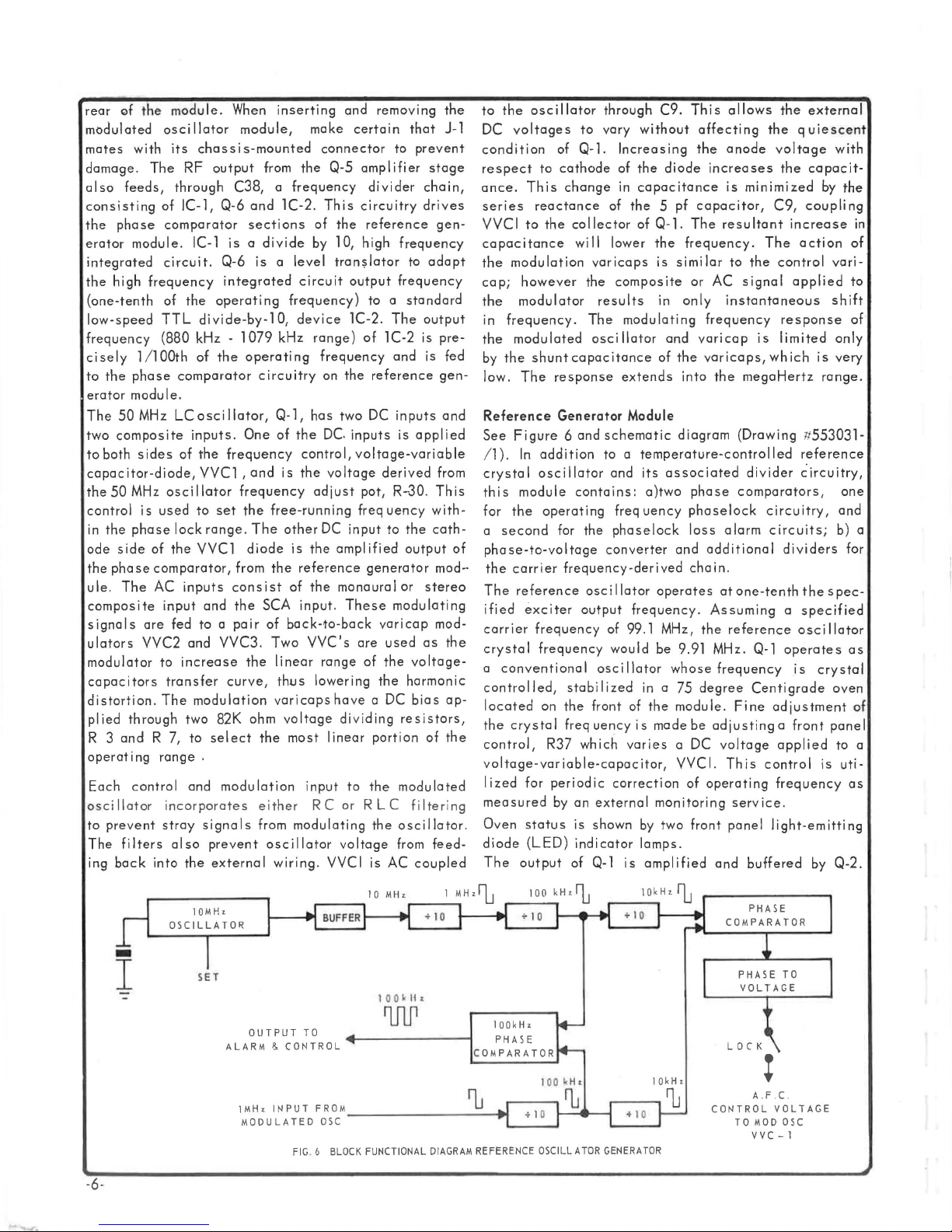
Reference
See
/
1).
crystal
this
for
a
second
of
phase-to-voltage
the
The
ified
carrier
crystal
a
conventional
controlled,
located
the
crystal
control,
voltage-variable-capacitor,
lized
measured
Oven
diode
The
of Q-l.
to
cathode
change
reactance
to
the
collector
wi
modulation
however
modulator
modulated
shunt
capacitance
The
response
Generator
Figure 6 and
In
addition
oscillator
module
the
carri
reference
exciter
for
status
(LED)
output
contains:
operating
for
er
frequency
frequency
frequency
stabi I ized
on
the
freq
R37
periodic
by
an external
is
indicator
of
through
to
vary
Increasing
of
in
of
the
II
lower
varicaps
the
composite
results
modulating
oscillator
extends
Module
schematic
to a
and
freq
the
phaselock
converter
-der
osci Ilator
output
of 99.1 MHz,
would
oscillator
front
of
uency
which
varies
correction
shown
Q-1
is
C9.
This
allows
without
the
capacitance
of
temperature-controlled
its
a)two
uency
frequency. Assuming a specified
in
the
is
by
lamps.
amplified
affecting
the
diode
increases
5 pf
capacitor,
Q-1
.
The
the
frequency.
is
simi
lar
or
AC
in
only
frequency
and
varicap
of
the
varicaps,which
into
the
diagram
associated
phase
phaselock
loss
and
additional
i ved
cha
i n.
operates
the
be
9.91 MHz. Q-1
whose
a 75
degree
module. Fine
made
be
adjusting a front
a DC
VVCI .
of
operating
monitoring
two
front
and
anode
is
resultant
to
instantaneous
alarm
at
reference
frequency
voltage
This
service.
panel
the
external
the
quiescent
voltage
the
minimized
C9,
The
the
control
signal
response
is
limited
megaHertz
(Drawing 11553031-
divider
comparators,
circuit
circuits;
dividers
one-tenth
operates
Centigrade
adjustment
applied
control
frequency
light-emitting
buffered
with
capacit-
by
the
coupling
increase
action
vari-
applied
shift
only
is
very
ronge.
reference
~ircuitry,
one
ry,
and
b) a
the
spec-
osci
Ilator
is
crystal
oven
panel
to a
is
uti-
by
Q-2.
for
as
as
in
of
to
of
of
OUTPUT
ALARM & CONTROL
1MHz
MODULATED
TO
INPUT
FIG 6 BLOCK
FROM
·6·
OSC
l
OOkl1'
W
FUNCTIONAL
lOOk H z
PHASE
COMPARATOR
ru
DIAGRAM
REFERENCE OSCILLATOR
....
1----.
•
..
10 I
l
OOk
Htl
~
~10
GENERATOR
10kHz
ru
1
A. F .C
CONTROL
TO
V VC - 1
VOLTAGE
MOD
OSC

Q
-3
is a shaping
tially
sinewave
compatible
is
heavily
produces
counter.
ves
IC-2,
is
in
of
the
parator
the
reference
IC-3
ference
rator.
1080
the
modulated
range
channel
a
NAND
rator.
respective
frequency
rical
When
with
and
Q-5
varying
departure
two
input
greater
average
an
value.
This
prase-to-voltage
of
Q-6,
rent
0-6
operates
C-14
off
when
ly.
Q-9
mizes
100kHz
SQUARE
WAVE
IN
IN
FROM
MODULATED
OSC
MODULE
with
driven.
square
The
another
the
88-108
inputs
as
well
is
in
the
input
Decade
kHz
range
and
is
phase
gate,
Both
Q-4
reference-derived
derived
square
the
carrier-derived
the
reference
wi II be a
from 0
from
signals
or
lower
output
comparator
Q-7, Q-8,
saurce
at
PU
PUT
zero.
the
serves
the
T
which
loading
~
amplifier
output
the
TTL
Its
wave
output
to
the
waves
as a
input
of
decade
kHz
of
the
phaselock-Ioss
as
to a third
oscillator
8.8
to
10.8
Q-4
of
dividers
carrier-frequency-derived
oscillator
carrier
comparator.
comprise
and
Q-5
input
at
generator
perfect,
to 5 volts,
exact
will
than
voltage
DC
output
converter
and
charges
switch
Q-8
switches
signal
as
an
on
7.5kHz
LOW
PASS
FIL
TER
which
of
Q-2
circuitry
grounded-emitter
outputand
IC-l
(880-1080
counter.
range.
divider
kiloHertz
the
main
IC-4
module
derived
This
and
Q-4
the
main
are
heav i Iy
pulses
the
paralleled
pulses
pulses,
50%
or
averaging
phase
50%
Q-9.
output
-
produce
duty
above
voltage
and
Q-7
to
goes
C-14
0-7500Hz
coincidence
C-14
set
the
emitter
while
changes
to
square
drives
Its
signal
decade
chain.
channel
IC-5
to
input
and
channel
frequency
and
are
duty
!Square
cycle.
or
feeds a combination
loop
acts
to
the
current
high
chargin~
...
wave.
which
follows.
configuration
IC-l, a decade
kHz
output
is fed to
alarm
divider,
The
range
andisthere-
phase
divide
pulses
the
8.8-10.8
to
Q-50f
Q-5,
connected
phase
overdri
and
produce
collector
exactly
the
output
cycle,
square
2.5
between
wave
This
below
the
fi
Iter,
as a constant
generate
initial
source
or
low,
follower.
DETECTOR
01.
02
the
essen-
output,
range)
frequency
phase
com-
IC-3,
output
compa-
the
880-
from
kHz
the
main
compa-
ven
by
carrier-
symmet-
output.
in
phase
of
wave
volts.
Any
output
results
2.5
volt
consisting
cur-
a ramp.
voltage
on or
respective-
It
mini-
the
output
-
-
filter.
ates
as a DC
differentials
Q-3
output
"lock"
dri-
q
uency
tween
I
ated-os
one
The
modulated
may
in
of
as
the
Q-4
the
of
in
on
be
ier
control,
placing
Q-l0
and
phase
(carrier-derived
lator-derived
to
the
the
output
to
DC.
cisely
output
the
input
are
modulated
difference
assume a departure
frequency
(1
x 10
channel
normally
the
modulated
output.
100
kHz
ten
times
The
100
Hertz
cuitry
7,500
7.5
MHz
Alarm
See
Figure 7 and
The a larm
3 STAGE
...
DC
AM
Q1
Q2 Q3
@®lJ(Q)I·
Thus
the
Q-6, Q-7,
loop
fi
Iter
at
the
phase
voltage.
switch,
control
the
c i
adjusted
the
lock
10kHz
When
in
of
3
-:-
phase
would
If,
comparator
kHz
rate
of
Hertz
at
and
P
This
output
SW-l,
reference-oscillator-derived
Ilator-deri
(R-30
front
Q-ll
comprise
loss
input
phase
of
the
the
phase,
the
comparator.
signals
by
in
the
of
100
1 x
10
comparator
osci
for
some
0.1
Hertz
square
would
which
representing a carrier
the
100
Control
and
input
ved
oscillator
by
the
on
modulated
panel
alarm
input
from
comparator,
Q-l
0,
two
100
vary,
the
input
of
MHz.
4
= 1 x 10-
result
Ilator
reason,
wou
or
wave
be
fed
responds
MHz
Module
schematic
control
AC
to
and
from
100
kHz
in a correction
J
LED~LQ.~~
Q-8
or
compari
front
lock
circuit.
and
integrator,
comparator
voltage
the
modulated
corrects
son
"free-running"
mounted
oscillator
switch
the
phase
It
IC-4
IC-2)
in an
operates
and
Q-4
Q-ll
comparator
kHz
input
square
If
the
frequency
the
resultant
component
frequencies.
1.0
kiloHertz
This
would
1
difference
)
operating
to
produce a precise
this
does
Id
produce
1.0
Hertz(10
signal,
to
the
alarm
to
input
operating
module
RELA
KI
O
-:
frequency.
Diagram
contains
-
Y
-
-
Q-9
circuitry
converting
input
is
fed
through
oscillator
any
difference
and
frequenc i es.
frequency
module)
in
its
off
comparator
at
reference-oscil-
identical
and
Q-5.
is
not
signals
waves
appearat
or
100
kHz
resulting
As
an
from
an
represent
at
at
10kHz.
voltage
not
c s
lip
frequency
3
3
-:-
10
= 1 x
interrupted
module,
frequencies
frequency
Dwg.
Ii 550161/1.
circuitry
-
-
~
occur,
oper-
phase
into a DC
the
fre-
be-
the
modu-
frequency
vern-
by
position.
for
the
100
kHz
manner
However,
fi
Itered
are
pre-
the
phase
of
pulses
from
the
example,
operating
0.1
Hertz
the
main
This
to
return
100
MHz
the
of
100)
at a 1.0
the
cir-
up
to
error
of
to
:
'
l
l
l
.
OSC
fo-900kHz
FIG.7
11
/ 73
Q4
2
BLOCK
FUNCTIONAL
DIAGRAM
ALARM
8.
CONTROL
MODULE
-7-

alert
the
operator
the
unit
if a
occurs.
The
output
in
the
reference
low
pass
filter,
kHz
components
parator
quency,
of
wave
a DC
switches
co
LED
at
strip
operate
a
shou
exciter
trol
DC
sensitive
lock.
in
the
absence
be
represents a division
tor
produces
pass
condition
at
ate
duce
backup
operation.
Fig.
cy
and
which
the
phase
output
voltage
Q-2
Ilector
loss
current
lock
1.0A,
28
of
the
an
of
phase
I d
be
relay
permitting
amplifier,
Loss
an
ouf-of-tolerance
center
frequency
of
made
manually.
of
1000
a 1 Hz
filter.
of
the
carrier
on
frequencies
submultiples
system
7. A crystal
of
carrier
indicator
to
to
frequency
of
thE:
generator
FLI.
produced
passes
would
lock
of
the
which
on
and
de-energ i zes
VDC),
exciter.
external
lock.
operated
contact
adjustment
Q-l,
insure
of
phase
phaselock
times. A carrier
signal
The
detector
7500 x 1000
frequency.
is
Refer
to
oscillator,
frequency -900
2
The
with
lated
lated
oscillator
an
oscillator
oscillator
output
operating
module.
module
loss
of
deviation
100
kHz
This
only
be
present
condition.
fi
Iter
is
turns
off
Q-3
"off".
appear
This
visual
Alarm
by a
closure.
Q-2, Q-3,
early
lock
operating
should
and
The
100
of
the
at
the
Since
which
suitable
employed
the
Alarm
frequency
frequency
The
is
phase
in
phase
module
filter
by
the
the
low
The
detected
transistor
off.
When
re
lay
The
contacts
on
the
termination
or
aural
loads
in
slave
re
R-5
of
the
threshold
to a point
detection
does
riot
be
closely
frequenty
kHz
comparison
carrier
frequency
output
responds
or
an
error
it
when
divided
for
phase
to
prevent
Module
Q-4,
operates
kHz.
is
signal
RF
amplified
lock
and
to
excess
comparatOr,
is
eliminates
100
frequency
in
low
Q-3
rear
excess
lay
is a sensitivity
necessarily
frequency,
corrections
frequency
of
to
is
doubled,
fed
input
by
of
fed
to a 7.5
kHz
phase
the
event
freq
uancy
and
converted
Q-l.
Thisaction
is
turned
K-l
and
turn s the
of
K-l
terminal
may
be
alarm,
indicating
of
actuated
condition
sufficiently
of
loss
However,
monitored
frequency
by a
error
of
the
7,5
a loS!!
of
up
to
possible
by
10,000
lock, a second
off-frequency
Block
at a frequen-
then
from
the
from
the
the
field
disable
100
kHz
located
kHz
any
100
com-
slip
fre-
of
loss
sine
to
oH,
(rated
barrier
used
to
25
watts
by
the
con-
of
of
phase
result
in
the
should
fac-
1000
Hz
kHz low
of
lock
7.5
MHz
to
oper-
pro-
Diagram,
mixed
modumodu-
effect
transistor,
intermediate
Q-7.
ter
provides a 900
detector,
shift
frequency
IF),
the
ficiently
is
turned
rent
of
contacts
The
normally
supply
relay
mounted
module
or
maintenance.
RF
Power
See
Figure 8 and
The
two-stage
imately
lator
pically
properly
The
the
drive
work
of
Q-l
output
push-on
module.
provide a relative
total
.47
ohm
this
DC
meter
The
RF
of
approximately 2 to
level
on/standby
of
the
from
abling
voltage
Q-5,
Q-7
drives a 900
D-6,
by
100
100
voltage
to
off
Q-l0
appearing
voltage
contact
On
the
is
removed
Amplifier
0.25
module
will
matched
RF
input
control,
comprised
matches
stage.
coaxial
RF
collector
resistor,
resistor
switch
output
from
switch
RF
module.
the
equipment
the
for
the
frequency
kHz
kHz
allow
and
en
closed
closure
R F
watt
to a rated
deliver
The
output
current
is
the
complete
and
fed
kHz
D-7.
If
or
more
removed
at
the
Q-8
Q-l0
erg i zes
on
to
the
main
frame,
from
Module
schematic
power
output
up
50
ohm
to
the
R-l
of
Cl,
the
input
RF
output
is
power
R4.
fed
to
is
in
power
modulated
SW-l
Thi s permits
following
RF
power
to
mixer,
output
kHz
the
filter
to
is
re
connector
contacts, 8 and
power
is
the
ampl i fi
to
first
and
C2
output
sampled
of Q-l
The
the
the
is
15
exciter.
of
band
IF
output
operating
(resulting
from
output
turn
on.
turned
lay
K-2
amplifier
by-passed
which
mounting
diagram
er i ncrea
level
of
10
watts
15
watts
load.
stage,
an
impedance
and
ll.
impedance
from
connector
by
output
and
voltage
front
Ipa
pOsition.
adjustable
watts
by
oscillator
is
provided
the
The
amplifier
Q-6
pass
signal
the
If
on.
and
terminals 8 and
operates
the
output
output
Q-l,
The
at
diodes
level
Q-2
penel
by
varying
removal
exciter
Q-6.
The
is
amplified
filter.
to
frequency
in a
mixer
norma I
wi
II
decrease
Q-8
turns
The
collector
opens
10,
connect
module.
by a
microswitch,
if
frame
for
Dwg.
::t
ses
th
modulated
level,
power
is
fed
matching
output
of
Q-2,
Q-2
appears
the
rear
Dl
indication.
passes
developed
meter
Rl
over a range
the
module.
on
the
front
of
without
+ 24V DC
can
be
900
kHz
The
fil-
the
diode
should
output
900
kHz,
suf-
on,
Q-9
cur-
the
re
lay
10.
DC
This
the
alarm
service
552073/1.
e a
pprox-
oscil-
and
ty-
into
through
netcircuitry
the
final
at
of
the
and
D2
The
through
across
when
the
RF
input
An
RF
panel
RF
power
dis-
supply
interrupted
by
a
a
to
a
R F
I N
A PR
1 4 W
PUT
OX
AMP
-8-
RF
Q 1
FIG. B BLOCK
RF
AMP
Q2
FUNCTIONAL
DIAGRAM
RF
POWER
AMPLIFIER
RF
REFERENCE
l-lSW
RF
OUTPUT
OUTPUT
11/73

at
several
the
Main
1)
The
2)
Channel-loss
control
3)
Main
alarm
4)
Standby
ule.
CAUTION:
operate
load,
amplifier
voltage
VSWR
2)
Amplifier
connectors.
pa
respective
tors
then
nectors
Power
See
The
DC
corporated
supply
A-5
divider,
+15
RF
is
Transistors
with
of D-1,
ohm
ficientto
under
good
represents
Use
extreme
ne I of
the
mounting
retighten
to
Supply
Figure 9 and
power
supply
for
.2
volt
volt
power
supplied
an
overload
D-2,
series
points
Functional
be
standing
Module
mounting
the
supply
IC-1,
supply
amplifier. Power
allow
in
the
Block
rear
term
ina
module;
frame-mounted
module
1)
engineering
operated
If
exc
Regulator
supply
voltages.
in
all
from a
Q-1
and
resi
is
switch
Although
normal
wave
a
transmission
care
to avoid
mi
sa I ignment
iter
and
bracket
hardware.
the
hardware
frame
.
schematic
regulator
the
module. These
logic
feeds
of
the
powers
+24 volt
and
Q-2
current
D-3.
stor,
R-11
current
exciter
I s
TB-2, 1 and
relay
removed);
on
the
the
conditions
practice
with a suitable
ratio
in
inserting
rea
Carefully
Module
Four
devices
the
modulated
all
act
protection
Current
develops a voltage
atthe
system,
Diagram.
contacts
microswitch (actuated
RF
power
RF
power
without a 50
dictates
of
less
efficiency
or
damage
I i gn
separate
high
source
to
occur
s,
the
by
loosening
securing
diagram
provides
and
phase
speed
oscillator
other
modules
to
the
RF
.
as a Darlington
drawn
bose
of
as
shown
2;
on
the
alarm
amplifier
amplifier
ohm
that
the
RF
load
with
than
2: 1.
of 89%;
removing
the
remove
con
nector
insert
the
(Dwg.:;552074/l)
all
regulators
include
100
power
ci
rcuit,
through
Q-1
the
push-on
the
s on
the
connec-
the
module,
coaxial
the
required
ore
a +5
comparators.
MHz
decade
module
except
amplifier
regulato
consi
the 0.27
drop
to
be
drained
on
and
when
Mod-
can
RF
RF
This
RF
coax
rear
the
con-
in-
volt
. A
the
sting
suf
from
the
Darlington
The
two
with
the
5 .6
ence
voltage
loss
of
Q-1,
5V, ± 10%,
meter.
exciter
a
and
urement
a
The
regulators,
with
the
The
i r
to
tively
be
i
metal
i
.
Q-7
the +24
on
main
voltage
at
requirements
F1,
regulator
occurs
power
r
former
Main
transformer
nection
The
should
discrepancy
the
specified
of
operation
the
schematic
+
15
that
used
high
measured
stor
Q-6,
chass
nsulated
and
Q-8
the
externa I heat
chassis.
from
approximately 1.25A,
is
provided
in
module
with
Block
wiring.
base
through
combination
forward
volt
sufficiently
Q-2
as
measured
DC
meter
be
between
the
actual
of
is
simi
exception
diagram
volt
supply
in
the
current
with
an N
PN
is
of
from
the
operate
volt
supply. These
Q-7
Z-l.
of
the
to
protect
the
regulator
are
three
Functional
connections
~o@l](Q)I·
the
load,
thus
biased
zener
.
The
provided
used
+5
volts,
voltage
the -5.2
lar
in
of
uses
+5V
supply.
all
modules
powe r devi
the
chass
as
si nk
and
The
24
well
RF
between
the
supplied
separate
Q-1,
Q-2
from
diodes,
diode,
to
DC
with a high
as a reference.
the
operation
the
for
supply.
power
is
with a mica
Darl
Q-8
volt
power
the
power
section. All
secondary
Diagram
and
D6
Z-3,
overcome
output
on
the
front
panel
verify
the
at
the
volt
supply,
to
current
nominal
regulator
This
The
output
properly
ce,
supply
ington
transistors
located
receive a base
supply
above
the
amplifier. A 1.5A
rectifier
transformer
by a
common
for
power
preventing
being
turned
and
D7
increase
the
DC
voltage
quality
front
ponel
In
the
meter
reading
modules
the
shutdown.
is
pass
on
is
the
.
with
+ 5
volt
voltage values.
circuitry
supply
voltage
inserted. Trans-
mounted
regulator
washer
tr'ansi
ore
the
top
current
maxi
mum
diodes
if a fai
voltages
power
winding. See
proper
supply
in
series
the
refer-
voltage
should
DC v
olt-
of
event
reading
by
meas-
Q-3,
Q-4
supply
Refer
similar
is a rela-
should
on
the
and
.
stors
mounted
of
the
reference
limited
current
fuse,
and
the
lure
to
the
trans-
the
power
intercon-
the
on.
be
the
of
to
is
in
IS
r
POWER
TRANSFORMER
11/73
FIG
12 V I A
CT
3SV
1.6A
.9
BLOCK
TO
OVEN
FUNCTIONAL
DIAGRAM
POWER
• •
SUPPLY
TOR E LA
REGULATOR
YS
-9-

Meter
Ampl
ifier
and
See
Figure
The
panel,
modulation
VU
cover
Q-1
lower,Q-2.Q-3functions
Rectification
circuit
follower
ter
resistor.
amount
compensate
plied
adjustable
The
·.'of
the
to a zero
Model
The
od
of
advantage
and
stal
ly
coupled
ter
follower.
plifier,
square
changes
voltage
si~nal
provides a dual
by
four
provides
degrees
sq
uare
operate
10
and
meter
amplifier,
is
used
to
signals
meter.
stereo
excellent
oscillator,
This
plate.
provides
of
of
to
input
amplifier
B-1l2Stereo
generating a stereo
drives
to
wave
of
Q-3.
with
the
Since
DC
for thi s
the
opposite
1 K
calibrate
VU
reading
generator
of
this
stereo
to
Q-7,
The
Q-8.
Q-8
wave
from
at a 76
switching
19
kHz for
two
38
out
of
voltages
as
high
ampl
flows
ohm,
operates
output.
the
Switching
schematic
located
amplify
sufficiently
is
ification
the
The
meter
so
Generator
method
a
output
is
kHz
function.
kHz
phase.
impedance
the
accessible
as
DC
signal
transistor
connected
the
meter
through
voltage, a reverse
side
zero
adjust
control,
that
100%
on
the
module
composite
separation.
at
buffer
stage,
of
heavily
The
full
supply
rate.
integrated
It
pilot
carrier
signals
The
drive
diagram
to
aDC
the
of
R-1,
meter.
Module
utilizes a switching
is
simplicity
76 kHz.
Q-7
collector
Thi s square
divides
two 38 kHz
Q-1
shun!
(Dwg. #551049/1).
behind
various
to
by
drive
takes
operates
is DC
the
modulation
overdriven,
voltage
which
the
audio
drive
the
removal
the
meter
drive
place
as
to a tap
coupled, a small
meter
to
voltage
meter
potentiometer,
sets
the
(Dwg. '0'559048/1)
signal.
of
Transistor
Its
output
operating
drives a shaping
voltage
value
wave
circuit,
the
76 kHz
output
and
are
Q-2.
ing
and
precisely
switches.
on
overall
corresponds
resulting
out-of-phase
Q-1
front
meter
frequency
front
panel
of
the
emitter
amplifier.
in
the
base
an
emitter
the
emit-
ground.
is
through
R-14.
meth-
The
prime
adjustment
Q-6,
a
is
loose-
as
an
emit-
of
to
76
IC-1. IC-1
signal
secondly,
and
They
top
fol-
To
apthe
gain
cry-
am-
Q-8
zero
kHz
180
Q-2
alternately
signal
When Q-1
in
and
composite
val,
13-14
in
the
setting
bration
bined
from
sine
plus
nal
to
range
to
lower,
modulator.
function
and
The
the
modu
pilot
in
panel
The
panel
mode.
at
adjusted
Q-5
cillator
by a
switch
coming
is
turned
its
"on"
state,
10
is
shunted
amplifier,
Q-2
is
turned
can
reach
the
collector
attenuation
of
these
and
Operation
signal
terminals
wave
derived
many
harmonics
switching
located
is
properly
produce a constant
Q-4,
out
of
providing
process
of
Q-3
on
the
a
simple
the
matched
fi
A front
justs
the
phase
insures
the
transmitted
amp
I i
tude
level
of
the
lation
would
carrier.
pi
19 kHz
switch,
terminals
to
relay
lot ampl
In
monaural
in
feed
module.
located
This
pi
9-10
level
the
out a segment
from
the
on, Q-2
the
to
Q-3.
off
Q-3.
250
leads
of
the
controls
in
Q-3
13-14;
from IC-1
of
Q-1
is
filtered
lower
top
by
Iter.
The
gain
a low
panel
of
the
proper
38
of
the
composite
include
amplitude
itude
control,
lot
carrier
SW-1,
placing
operation,
and
and
monaural
The
above
on
input
is
input
ground,
During
and
an
ohm
of
Q-1
two
transistor
wi
II
section
consi
sts
the
19 kHz
generated
and
by a 53
cover
the
group
output
stage,
impedance
pilot
transmitted
timing
kHz
switched
pi
lot
is
10%
may be di
13-14
connected
signal
switching
the
module
of
terminal s of
turned
signal
hence
input
controls,
and
be
of
through
Q-2.
input
delay
of
and
phase
of
signal.
injection
is
R-47.
the
the
are
from
cannot
the
signal
Q-2,
switches.
covered
the
manual.
of
the
pi
lot
in
the
The
kHz
of
the
and
over
the
fi
Q-5,
output
control,
19
the
transmitted
composite
norma
Ily
Thus
established
sabled
system
audio
resi
stively
directly
to
the
itself.
the
audio
the
off.
When Q- 1
terminals
reach
same
time
on
terminals
R-11
and
serve
to
in
the
The
chopped
which
a 19 kHz
square
composite
low
pass
unit.
This
output
the
frequency
Iter
is
connected
an
emitter
to
drive
kHz
pilot.
set
at
100%
of
the
by a front
by a front
in a
monaural
input
combined,
to
modulated
is
accomplished
The
relay
input
module.
inter-
R-12,
balance
Correct
Cal
com-
signal
is
now a
fi
Iter;
wave
filter,
filter
ci rcu i
R46,
This
pi
signal.
1I10th
total
19 kHz
signals
Q-4
is
9
the
i-
sig-
ts
fol-
the
ad-
lot
and
os-
can
COMPOSITE
IN
J
1
1
ST
f
IN
PU
T
CONTROL
-10-
a I
GAIN
AGE
J
l
--'"
02
EMITTER
FOLLOWER
FIG
10
BLOC·K
FUNCTIONAL
03
OETECTOR
AND
METER
DRIVER
DIAGRAM
METER
~r---7lH
~L....LJ
AMPLIFIER
D.C
ZERO
TO
METER
11/73

be
controlled
by
an
externally
minals
in
stereo
Model
The
able
kHz.
tions
quency
of R-16,
the
the
signal
is
put
R-3,
modulation
Q-1
lower
to
pre-emphasized
gain
The
frequency
ter
consisting
resistor
ing
of
beIng
wave
sisting
form.
filter,
isolation.
potentiometer
tion
The
and
of
vides
age.
tified
ronic
voltage
combination
circuit.
istor
indicating
Thet
and
TB-2, 7 and
the
mono
modes.
8-113
SCA
Generator
on
two
Dual
transistor
as
the
is
primari
R-20,
pos
ition
front
panel
is
also
frequency
of
F L-1 is
which
acts
and
Q-2,
to
provide
properly
output
follower
circuit.
emitter
level.
emitter
adjusts
Q-7.
regulated
modulate
of
Q-1
of
modulated
Q-4,
of
diode
follower
transmitted. FL-2
harmonics
only
To
prevent
Q-S,
an
The
Q-7
40dB
The
limiter
DC
output
mute
switch,
is
bled
The
Q-8
on,
lamp
35-40
volt
11173
by
the
front
connected
8.
The
position
SCA
standard
free-running
of
bandwidth
level
for
Generator
(Module
frequencies,
Q-3
Iy
determined
C-S,
C-8
R-10,
the
fine
adjustment. The
applied
connected
both
serve
to
limited
as a load
control. The
as
the
necessary
remote
(a
and
coar
the
an
Q-3.
frequency
as
the
modulation
Q-3
is a 41
signal
through
R-21, R-22, R-23,
switch
The
67 or
and
of a
frequency
emitter
output
R-29
of
Q-2
the
modulation
functions
of
limiting
output
voltage
off
which
presence
allowing
mounted
unregulated
by
trans i stor Q -6.
a DC
is
used
41
kHz sq
Q-4
must
eliminates
produces a clean
undesirable
follower
level
to
vary
is
connected
as a limiter
to
voltage
is
R-21,
R-23,
to
ground
functions
of
the
current
external
panel
switch
front
panel
selection
(Dwg.
position 2 or
matched
master
by
the
se
adj
bases
by
filter
to
a 1 K ohm
to
the
following
ampl
ifier
level
C-2
produces
response
frequency
kHz or
which
voltage
to
provide a silent
uare
be
filtered
modulated
loading
provides
from
Q-S
the
SCA
to a 2.SK
voltage
the
sampled
is
used
to
D-6,
through
as
a var
mute
to
flow
source
switch,
closure
control
of
It
559049/1)
either
41
silicon
oscillator.
the
time
voltage
ustment,
audio
of
Q-3.
FL-1,
potentiometer,
fi
Iter
and
and
pre-emphasi
the
by
increasing
is
67
kHz
is
coupled
controlled
and
D-6, D7.
wave
by
the
unwanted
subcarrier
sinusoidal
of
the
the
is
controlled
sub
level
ampl
ifier.
modulating
rectified.
turn
on
and
D-7.
the
iable
voltage
through
to
the
SCA
voltage
or
remotely
across
must
the
mono/
3)
is
avai
kHz or
pair)
func-
The
constant
appl
ied by
and
R-ll
modulating
The
audio
The
and
as
two
stages,
emitter
necessary
increased.
square
carrier
to
swi
signal
FL-2
square
low
necessary
control,
to
the
wave
emit-
before
wave-
Q-7
The
the
elect-
The
R-44, C-21
mute
delay
turns
trans-
the
module.
is
filtered
ter-
be
67
fre-
out-
the
fol-
the
tch
The
mut-
out
con-
pass
by
injec-
R-9,
input
pro-
volt-
rec-
mute
LED
Turning
Place
Amplifier
tion.
Connect a SO
1-
Actuate
switching
to
insure
Obtaining
Rotate
this
position,
tor
is
tion
while
turn
on
100%. Within
modulated
Slow
s
ence
matically
the
LED
few
seconds
the
50
the
modulated
to
the
the
control
is
not
control.
the
reference
vern
ier
or
the
the
vernier
other
rotation
the
control
assume
a
few
tion
for 100%
Setting
No
attempt
made
in
operation
temperature.
temperature
control
adjust
monitor
frequency
Adjusting
With a
output
on
the
PA
module
Connect
power
to
proper
Phaselock
the
meter
connected
resistor,
observing
the
exc
osci
oscillation
of
the
AC sl ip freq
attained,
indicator
MHz
vernier
left,
then
negatively,
attained,
Check
frequency
unit
is
frequency
until
lock
of
the
to
goodrelock
hours
of
the
Station
to
unti I the
on
the
the
freq
or
to
measuring
the
properly
of
the
~°®lJ(Q)I·
V.
OPERATION
Exciter
drive
in
AC
power
ohm load
switch.
the
tSV,
operation
switch
the
output
to
the
R-14A.
the
iter.
15
seconds,
Ilator
of
the
the
on
later.
To
freq
oscillator
to
the
the
to
be
generator
control
extremely
is
attained
control.
position
if a
operation,
reading.
Frequency
adjust
system
long
enough
Allow
to
stabi
reference
uency
concur
RF
Output
matched
B-910
FM
control
its
Turn
The
approaches
the
meter
certain
30
I i
to a properly
service.
located
extreme
to
Check
-SV, t lSV,
to
of
meter
phase
meter
uency
quivering
verify
uency
right.
then
is in
cold,
control
After
the
loss
the
is
minutes
ze.
with
exciter,
counterclockwise
to
terminals
the
exciter
DC
of
the
phase
the
10
through a 4.7 K calibra-
the
exciter
lock
meter
shou
the
meter
needle
signal.
alarm
module
pro,Per
control
module
The
positively.
wi
II
not
the
the
ha s
been
cantinue
from
and
lock
meter
ofAC
recheck
station
phase
to
reach
The
fron t
osci
lIator
measurements
50
ohm
flip
on
the
TB-1, 1 and
RF
meter
and
+24V
the
power
lock
kHz
phase
off
meter.
Id
come
will
the
lock
is
due
As
wi
II
stop
wi"
phase
R-30
front
panel)
meter
should
follow
phase
lock
lock
pasition.
improper
to
one
extreme
the
meter
is
attained,
at
100%.
power
the
phase
frequency
locked,
for
load
and
normal
the
pane I frequency
module
calibrated
connected
the
RF
RF
Power
output
readings
positions
suppl
position.
compara-
momentarily
Once
again,
up
to
quiver
If
slowly
freq
to
the
lock
abruptly
come
lock,
(located
phase
the
switch
Iy
ad j usted
follows
This
occurs.
lock
should
has
operating
crystal
is
frequency
taken
on/
as
uency.
is
adjust
slowly
follow
vernier
If
adjust
to
rotate
used
to
standby
posi-
2.
jack.
by
ies.
In
near
the
pres-
auto-
and
on a
on
lock
on
the
the
the
wi
After
posi-
be
bee
oven
to
by a
the
-11-
II
'n

switch
th e
Adjust
ing
The
corresponding
the
trol
shou
Normally
approximately
The
meter
per
wattmeter
adjust
output
Ipa
cond
Connect a 400
terminals
signal
mately + 10dbm.
located
position.
desired
FCC
position
tion
semi-peak
100%
When
must
100%
respond
perienced
located
"on"
the
the
Ipa
meter
RF
output
until
the
Id
the
PA
and
output
the
power,
current.
ition
Monaural
level
on
percentage
type-approved
the
and
modulation
feeding
be
made
modulation
to
po
sit
PA
meter
is a 0-1
desired
fina I current
an
RF
position
is
only
is
in
series
PA
or
Either
for
the
Audio
located
feeding
the
Adjust
front
adjust
reading
complex
intermittent
wi
th norma I
on
the
i on .
drive
control
position.
ampere
to
lA.
As
wi
II
increase.
RF
output
600-900
scales
used
obtained,
with
tune-loading
adjust
procedure
power
ampl
Hertz
audio
on
the
the
Position
front
of
the
the
audio
of
modulalion
panel
the
level
device
with a sine
wave
to
maintain
point
since a semi-peak
program
RF
Power
meter
the
o~tput
read
of
10
milliamperes
the
as a reference.
either
the
the
loading
rear
exciter
the
module
level
modulation
meter
accordingly.
and
program
modulation
peaks
clockwise
in thi s
PA
Advance
is
achieved.
i n9
watts
meter
connect
output
controls
wi
II
ifier
output
source
of
the
flat
Ipre-emphasis
to the.
monitor.
switch
is
calibrated
wave
of
short
materi
Ampl
drive
exceed
is
to a 0-28
coaxial I ine
for maximum RF
control
result
to
the
exciter.
should
to
the
os
in
audio
material,
peaks
a
I.
ifier
Modu
while
monitor-
position,
is
increased,
the
drive
In
no
1
ampere.
achieved
of
PA
Current.
volt
After
the
an
in-line
for minimum
in a
resonant
network.
proper
The
be
approxi-
pre-emphasi
exciter
indicated
Alternatively,
the
audio
The
meter
to
display
input
allowance
below
meter
duration,
Ie to
100%
con-
case
with
DC
pro-
RF
and
input
audio
switch
for
the
on an
posi-
is
signal.
the
cannol
as
ex-
REFERENCE
Osci
lIator)
Place
extender
1.
Turn
tion.
Adjust
2.
lator
Pos
3.
front
Connect
4.
Q-3
FCC
should
If
the
tate
direction
sired
range
frequency
5.
Adjust
(lOOK)
REFERENCE
age
1.
Connect
ing
2.
With
form
MHz
Just
be
If
shown
R-19,
ramp
is
normally
Converter)
similar
the
s
a
VI.
CALIBRATION
GENERATOR
the
reference
card.
meter
switch
inductor
voltage.
iti
on
the
frequency
of
the
module
a
frequency
or
observe
type-approved
be
within
frequency
the
slug
to
bring
frequency.
wi th
the
correction.
the
Reference
for a 100% '
GENERATOR
an
osc i II
capacitor,
the
system
across
oscillator
prior
amplitude
eliminated,
the
to
phase
to
Fig.
observed
in
Fig.
slightly
will
generator
to
L-l
to
the
frequency
frequency
1 kHz
deviation
in
inductor
the
This
front
oscope
C-14.
in
capacitor.
vernier
11
wave
12,
in
until
as
phase
operate
PROCEDURES
MODULE
module
the
Reference
for maximum
ad j ustment
its
mid-position.
counter
mon
of
the
is
greater
L-l
frequency
will
insure
contro
I,
Oscillator
ading
on
MODULE
to
the
phase
lock
below.
adjust
the
theglitch
lock,
until
loss,
form
the
direction
lock
in
its
Slowly
the
is
full
(
Oscillator
reference
to
the
of
the
itor.
desired
in
closer
sufficient
to
perm it
calibration
the
front
(Phase
.005
tanta I um
observe
advance
system
the
wave
more
ramp
voltage
which
on
the
is
lost.
clockwise
Reference
on
the
module
oscil-
control
exc
The
than 1 kHz;
the
similar
leading
on
collector
iter
with
frequency
frequency.
appropriate
to
the
tuning
long-term
pot
panel
meter.
to
charg-
the
the
loses
form
should
to
control,
lowers
edges
This
control
position.
posi-
the
of
an
ro-
de-
R-l
Volt-
wave
50
lock,
that
the
0
Stereo
Audio
Conr.Ject
channel
Adjust
-1
Operation
suitable
terminals
left
input,
the
Pi
lot
Level
Remove
justed
of
pi
erator
the
FCC
measuring
lot
level,
modu Ie for 8-10%.
?-
sources
on
TB-3, 5 and
levels
as
described
audio
from
type-approved
the
19
located
on
of
the
6;
the
kHz
the
audio
rear
af
right
input,
in
exciter.
modulation
pilot
front
panel
to
the
left-
the
B-910
TB-3, 7 and
the
monaural
With a
monitor
injection,
of
the
and
exciter;
section.
properly
capable
adjust
stereo
right-
ad-
the
gen-
8.
----J
FIG.
11
L-I--'
FIG.
'--
12
11/73

MODULATED
Place
the
card.
1.
Turn
generator
2.
Position
mid-position.
3.
Position
4.
Connect a suitable
the
RF
required
to
prevent
5.
Position
near
6.
Connect a 100
to
the
7.
Slowly
the
phase
the
coil
the
beat.
dication
8.
Flip
snap
the
LED
should
9.
Observe
the
doubler
10.
Adjust
L-l1,
these
11.
Observe
quency
sired
12.
Remove
watt
13.
Adjust
for maximum
should
res i sti
MONAURAL AUDIO
1.
Connect
internal
put
quency
the
output
2.
Adjust
3.
Set
an
4.
Vary
recording
sary
tenuation
dard
in
section
A
reproduction
is
included
OSCILLATOR
modulated
phase
their
the
to a
carrier
non-inductive
termi
the
to
75
lock
modu Ie).
the
vernier
meter
output
between
damage
all
coil
mid-position.
RF
output
adjust
lock
slug
Set
as
possible.
phase
steady
lock
come
on
the
coil,
the
three
and
L-14,
inductances
the
mon i tor.
operating
the
counter
the
series
be
between 3 and 5 volts
ve
load.
an
accurate
or
external
no
I s
response
terminals.
the
input
output
input
the
maintain a constant
settings
mi
crosecond
73.3330f
following
osci
switch
frequency
switch
100
jack
(J-l).
the
to
the
slugs
MHz
jack.
the
oscillator
meter
for a low
very
slowly
the
slug
lock
position
indicator
after a few
output
frequency
output.
level
attenuation
voltage
L-6,
remaining
for max i
wi
II
The
and
resi
output
MODULE
col
and
on
over
level
reference.
frequency
should
the
of
the
MODULE
lIator
module
off
(located
control,
in
phase
lock
MHz
frequency
CAUTION: A pad
exciter
oscilloscope
as
switch
for maximum 100
be
frequency
frequency.
stor.
The
signal
a
at
pre-empha
this
latter
(L-2,
as
close
indicating
on
the
seconds.
of
sluga
mum
extremely
on
the
repl
ace
coupling
final
ibrated
output
SO
to
250
between
of
the
output
follow
FCC
Rules
standard
section.
output
unit.
L-6,
L-8,
Or
coil,
frequency
it
is
possible
to
the
on.
The
alarm/control
the
in
Olltput.
counter
shou
wi
capacitor,
RF
across
generator
attenuator
vol
tmeter
15,000
Hz
to + 10
50
input
voltage.
closely
sis
and
pre-emphasi s curve
on
the
extender
on
reference
R-30,
in
its
position.
counter
and
the
L-ll,
RF
voltmeter
L-2,
and
beat.
zero
meter
phase
module.
MHz
inductor~
The
tun
broad.
or
Id
be
th a
47
voltage
the
with
to
of
Hz
range,
dBm.
and
15,000
signal
the
curve
as
Regulations.
may be
counter
L-14)
watch
Turn
to
miss
beat
.hould
lock
module
Adjust
dUtpUt.
L-8,
ing
the
the
ohm, 1-
C-37,
output
47
either
the
flat
neces-
The
stan-
shown
to
in-
and
of
fre-
de-
ohm
in-
fre-
to
Hz,
at-
5.
If
the
measured
scribed
slightly
capacitor,
switch,
6. Do
filter.
adjusted
ductor
justment.
ALARM AND
Connect
card.
module.
per
frequency
Fc(MHz} =
Oscillator
1.
Connect a voltmeter
point
bler
2.
Adjust
imum
direction
age
mately
This
the
Doubler
1. Adj
in
point.
The
volts
R F Coi I
1.
Connect
istor,
mediate
maximum
peak-to-peak.
Off
Frequency
1.
Temporarily
socket.
the
insert
(relay
curve,
by
SW-l.
not
alter
This
at
sore
the
alarm
Check
for
Use
the
fo+900kHz
Adjustments
TP-l,
coi
Is,
the
voltage
to
reoding.
10·15%
will
unit
is
Adjustment
ust
the
the
output
Set
final
DC.
Ad i ustment
an
Q-6,
frequency.
900
Adjust
point
the
de-energizes.)
varying
C-6,
the
epoxi
CONTROL
of
L-3
slug
insure
turned
doubler
the
voltage
(the
where
crystal.
~o@IJ(Q)I·
response
the
the
in
the
adjustment
is
an
extremely
factory.
ed
and
proper
formula
the
crystal.
:2
located
and
L-2.
in
the
at
the
increase
Adjust
below
reliable
on.
voltage
slug
reading
oscilloscope
mixer),
kHz
output,
Detector
remove
the
the
K-2
does
pre-emphasis
value
of
series
in
control
frequency
with
between
test
the
the
coi
for
Adjust
Threshold
K-2
coil
with
of
stable
The
tuning
place
MODULE
module
below
for
or
a 5
theoscillator
oscillator
point.
inductance
slug
maximum
crystal
I,
L-2, for a
observed
the
exact
will
to
the
Observe
the
which
the
crystal,
threshold
of K-2
contacts
not
follow
may
the
nominal
the
pre-emphasis
the
15
kHz
filter,
slugs
after
fi
na I
to
the
crystal
determining
Fc(MHz} =
volt
range
coil,
L-3,
Rotate
for a
be
the
for maximum
reading
voltage
starting
noticeable
at
the
minimum
between 1 and
collector
the
900
RF
coi
is
typically 2 volts,
Xtal-1,
control,
just
energizes.
should
the
be
low
precisely
in
factory
extender
in
the
fo-900
to
the
and
for
slug
approxi-
obtained.
whenever
above
reading.
of
kHz
I,
L-1,
from
R-33,
then
pre-
altered
1500
pass
the
in-
ad-
alarm
the
pro-
kHz
2
test
dou-
max-
in a
volt-
dip
test
trans-
inter-
for
Re-
reopen,
pf
2
its
to
11173
-13-

Phase
1.
2.
3.
RF
modu
the
Ampl
2.
3.
5.
Lock
Turn
the
tate
the
oscillator
position.
Adjust
relay
Turn
just
trol for
relay
Remove
1.
Connect a cal
Connect a high
output
meter,
waveform
harmonics
Switch
,' ing of
4.
Sw
correct
front
6.
7. An R F
eres
8.
for
9.
50
the
K-1
the
the
phase
K-1
POWER
the
Ie,
remove
Alarm
and
ifier
.
jack
(J-l)
Jack,
C-14
for a maximum
and
to
ascertain
the
between
indicated.
itch
the
tween
22
p,eat
step
Return
milliamperes
reading
Observe
wattmeter
with a total
Adjust
si
recommended
Switch
adjust
a
reading
and
brated
power
the
paMI
output
.
the
red
RF
which a B-910
the
the
100%
is
not a precise
RF
ohm load
readings
Loss
Threshold
phase
lock
vern i er
modulated
AMPLIFIER
Ipa
is
read
is
frequency
module
loss
is
phase
should
RF
Control
on
simultaneously
as
and
DC
DC
and
between 8 and
the
and
output
wattmeter
to
of
lock
de-energized.
lock
lock.
energizes.
Power
the
Reference
ibrated
the
rear
frequency
adjust
atthe
same
displayed
spurious
Meter
600
Meter
24
volts
and
Epa
2 unti I
DC
Meter
RF
Drive
is
indicated.
indication
adjust
power of
lpo
current
front
panel
power
required
is
DC
Meter swit"ch
RF
Sample
i ng
on
relative.
should
are
switch
switch
osci
After
module
C-1, C-2, C-7,
and
sw
correct
being
the
It
terminated
be
to
to
control
the
extreme
threshold
to
Ilator
ver,nier
approximately 3 seconds,
MODULE
Amplifier
Osc i Ilator
to
gain
RF
wattmeter
of
the
exciter.
osci
signal
function
readings
control
indication
as
observe
time
that
shows
signals.
900
millamperes
itch
to I pa, a read i ng
DC
should
readings
switch
C-13
be
to
until a reading
The
12
watts.
of
RF
for maximum RF
10
watts
of
less
RF
Drive
(10
watts
RF
drive
used
to
Calibration
meter,
is a sampling
used
whenever
made.
the
off
position.
on
the
modu I
counterclockwise
control,
its
on
cover,
access
to
Iloscope
shown
the
the
the
minimal
switch
be
are
not
Epa
RF
output
shou
than
control
for a
for
as
an
the
The
of
RF
with a non-inductive
R-5,
position
freq
uency
reinsert
modu I e
to
the
RF
to
the
C-8, C-13,
on the
osci
Iloscope
sinusoidal
amount
to Ipa, a
should
indicated.
obtained,
are
obtained.)
and
adjust
output
power on
I d
be
obtai
900
milliamp-
for
B-910T
the
transmitter
exciter).
RF
position
control,
R F
output
of
RF
power. A cali-
absolute
the
output
of be-
of
ot
output.
the
or
R-6 for
voltage
Ro-
ated
until
. Ad-
con-
the
and
RF
RF 5.
and
watt-
RF 6.
of
read-
be
(If
re-
the
800
this
the
ned
dethe
and
meter
RF
are
zener
diode
ments
are
required
NOTE: A 1)12
module
STEREO
1.
2.
3.
4.
7.
8.
9.
GENERATOR
Place
card
Connect
and
B-910.
Locate
minals
Connect
level
adjust
left
total
meter
Switch
19 kHz
e I
pilot
Switch
leftmanner
phase
Adjust
Connect
terminals
be
control,
Observe
kHz
stereo
arrow
below
the
provided.
an
pilot
the
located
to
the
the
channel
modulation
of
the
the
pilot
contro I located
injection
the
and
wh
with
the
readi
Iy
R-31).
the
phasing
generator
heads
in
referenced
or
Amp
fuse,
protecting
stereo
frequency
an
composite
stereo
signal
right-channel
i ch
the
level
an
of
connected
Fig.
generator
FCC
Type
left
and
on
the
audio
left-channel
modulation
monitor
stereo
modulation
injection.
on
.
generator
wi
II
left
for 100%
oscilloscope
the
stereo
bow-tie
control,
module,
exactly
13.
and
possible
source
modulation
(L =
horizol1tal
(Fig. '14, i
.
F-1,
the
RF
MODULE
Approved
Monitor
right-channel
rear
apron
of
audio
output
indicated
and
Adjust
the
front
audio
have
the
-R).
total
generator
to
the
waveform
located
no
is
located
Power
module
to
250
level
90% on
monitor.
monitor
the
of
to
100
input
right
modulation.
to
the
arm of
and
on
to
phase
to
ncorrect
calibration
inside
amplifier.
on
the
stereo
the
of
Hz
input
the
module. (This
each other
modulation
output
audio
the
control
by 100%
19
Hz.
composite
adj
the front
input
exciter.
at
a + 1 0 dBm
terminals
for 100%
the
left
to
monitor
kHz
pilot
modu Ie for 10%
Parallel
terminals
channel
the
output
ust
the 19-
the
hori
as
adjustment)
adjust-
of
the-
extender
of
the
ter-
and
on
the
channel
the
lev-
the
in
out-of-
output
can
level
38
of
the
zontal
shown
a
.
POWER
All
REGULATOR
output
DC
voltages
MODULE
from
the
Power Regulator
-14-
Module
FIG.
14
11173

10.
Feed a 400
11.
Adjust
the
amplitude
the
Repeat
12.
connected
just
Select
13.
base
adjust
R-20,
the
composite
base
line
steps 9 and
the
right
an
audio
line
of
the
filter-matching
and
R-24
lines
Hz
signal
oscilloscope
waveform.
switch
to
as
control
as
shown
the
right
channel
frequency
the
composite
for minimum
shown
to
the
to
Adjust
for minimum
in
Fig.
FIG.
15
lOw
channel
amplitude
near
series
in
Fig.
left
channel
properly
15.
ith
the
input
control.
10 kHz.
wave
phase
16.
input.
synchronizeon
the
left
channel
curvature
signa I generator
termi
no
Observe
form.
Alternately
and
shunt
trimmers,
error
and
straight
(Fig.
17,
improper
ls.
17.
in
18.
19.
20.
Ad-21.
the
Front
Remove
compartment
calibration
1.
2.
3. T
4.
5.
6.
sary)
of
±
0 Hz,
with
Connect
minals
in-phase
L = + R.
nel
for
50 -15,000
Repeat
feed
L - R
Measure
should
Position
mono
Adjust
100%
+10
nel
Remove
Place
if
Adjust
meter
Re-insert
modulate
wave
tion
Adjust
100%
of
into
the
measurements.
step
L=
- R
into
be
position.
the
reading
dBm, 1000 Hz
input
Panel
top
adjustments.
all
the
emporar i Iy
used.
the
amplifier
signal
monitor.
the
as
~°®lJ(Q)I·
the
19 kHz
the
the
signa I generator
the
signals
Measure
L - R
Hz
16
signals,
L + R.
the
suppressed
below
the
front
monaural
on
terminals.
Modulation
cover.
directly
input
meter
remove
DC
balance
the
stereo
the
transmitter
as
input
indicated
signal
trimmer,
exciter
to
the
the
channel
Complete
spectrum.
except,
1%.
panel
gain
the main
signal
Meter
The
meter
behind
audio
select
the
card,
for
generator
indi
cated
cal
ibration
on
for
C-11.
to
in a manner
left
and
crosstalk
using
the
connect
and
measure
38
kHz
stereo-mono
trimmer
channel
connected
ampl
the
meter
signals
switch
control,
the
stereo
zero
100%
by a cal
control
front
.
in
reading
with a 1,000
exactly
the
rear
which
the
right
of
the
the
stereo
above
the
the
carrier
switch
control,
monitor with a
totheleft
ifier
located
panel
the
Audio
generator
R-14,
located
on
module
ibrated
R-1 for
panel
meter.
19,000
aud
i 0
will
channels,
L + R
monitor
across
generator
crosstalk
level.
in
R-2, for
in
has
position.
modu Ie,
on
the
meter.
if
used,
Hz
modula-
exactly
Hz,
ter-
feed
chan-
the
to
of
This
the
chan-
the
two
the
and
sine-
FIG.
17
14.
Check
modulation
into
than
and
15.
Recheck
justment
output
16.
Check
ing a
justment
11/73
the
stereo
left
measurements.
35
dB for
15
kHz.
steps 3 and
of
level
the
frequency
control.
audio
monitor
adjustment.
frequency
the
for both
all
pilot
counter
Adjust
separation
Separation
freq
uenci
4.
This
level
of
the
to
the
left
control
19 kHz
the
using
into
should
es
between
will
be
and
pi
lot ampl
frequency
right
the
pilot
the
stereo
and
right
be
greater
50
Hertz
final
ad-
composite
connect-
itude
ad-
(if r'!eces-
B-113
SeA GENERATOR
1.
Position
card.
2.
Connect
and
modu
exciter.
3.
Adjust
actly
67
trol
positioned
4.
Pos i tion
position.
5.
Connect
±2,
dBm,
6.
Adjust
modulation
7.
Adjust
subcarrier
the
SCA
generator
an
FCC
Type
lation
mon
i tor
R-10,
the
coarse
kHz
with
the
front
approximately
thel flat /pre-empha
an
audio
signal
to
the
rear
audio
R-29,
the
Injection
as
indicated
R-3,
the
Modulation
modulation.
module
Approved
to
the
frequency
panel
sis
source
input
Level
on
the
Level
output
fine
in
the
swi
tch
of
terminals
control
SCA
control
on
an
extender
SCA
frequency
of
the
control
frequency
mid-position.
in
the
1000 Hz,
.
for 8-10%
monitor.
for 100%
B-910
for
con-
II
fl
+10,
ex-
at"
-15-

8.
Reduce
the
waveform
peaks
holding
Mute
just
the
the
input
level
at
start
SeA
the
signal
control
output
to
cl ip.
carrier
level
R-9, whi Ie
of
Q-7
This
will
on
and
by
40
unti I
prevent
wi
II
dB
and
observing
the
wave
noise
avoid
unwanted
adjust
the
form
from
dropouts
9.
Remove
delay
mute
iod.
of
the
for
delay
carrier.
audio
input
the
carrier
potentiometer
signal
to
and
squelch.
for
the
observe
Adjust
desired
the
R-M,
delay
time
the
per-
VII. S TAN 0 A R 0 P R
7 . .' J H
·1 . q
6
5
4 -II I
3 I IIPlIIIII
2
1 1
o
9
8
7
"'
1
Qi
~
6 '. "
~
o ,
5 .
:.
2
o r
·1
-2-
If
tl
1111
III
!
01111111111
1
111'1'11'1.
.,
;#,
1ttt
!:W
L
ttr.~"
-:T
.
fit
fHj
~;
w.
::
~
~
~
1
...
..
.
.::'
,
:::\ ..
f-
ff
H.
~
7:l~
i
•
..
1
STANDARD
TIME
Frequency
. LJashed
. ,
. .. .
'.
,- ,
1;'
..
' ,
::::
:.
::~..
:::.'" .
..
.
~
,.,
:-1
-
~
•
PRE·EMPHASIS
CONSTANT
Shown
Solid
ft
~
....
...
~._
;
.
i
It
.~
..
+·
:
75
'd
L'
(S
I
o I
Response
by
and
01
' ;'
:1i
:
_.
1=
fii
~ ::)
.,
-1t-:.lli!t:+;:1
'
_,
:r:
:.
';
.
..
I
II
MICROSECONDS
me)
use
.
~~
OJ , ..
~~;:
~
E-E
MPH A
"H,.I;:f~
·::1··
..
+
+++!l...
CURVE
Limits
of
Lines
f
;F ::::
:.: .:.-
..
..
....
:
:-.1 .::: :
:..
:::-
!:
r~::
~
' ,;
'::
~..;::
--
I
. ,
•
.:
.. ::: :'''
:·
.:
. . .
,
:+
-
.. .
......
. "
.
...
-
I'
...
. t
::1 .
...
"
!=J;
SIS
,
H-
~~
' .
,-
CUR V E
G'I+!-l
&.
t-t
t-
~t
+i
·
'''1\
I
:.iLi
r+t+
·rn ....
..
...,.~:i,
~'
r~I"'"f
.
,.,
........
,~..
.
t " "
t -
~
I"
:'
: . ::::
.......
:
;:::
-Ii"
T'U,
H+Hfl·J ::
L1
111r:;:
Bi
Ir!··I
n mHh i'
tt
U
~WI-U
W
m!tt!
.
~
LI .
'
,1-
'.-,
f,
i.l1
H nw
.
,.. ..•
h.
1-..w ~ .1. : _
l
ilt· ..
~II;
pu
..
.. ,
.
;~
; ;~~
Ilit : ..
... ·,10
il. ...
...
iHlfll
..
I::J~:
:
::::::;::
...
: "
"
...
... "'Lt:±r'
..
...
~
.::
".;
'
~:--.
.......
..
... . ...
:;~
:::
~
r ....
::
: ::
i:
n!' ::::
rI'::::
.
,.
"~I'~
f.I
..
-·
'1'
f!-;
,::.11'
iJ ... . Y ;i:
~t.
·
"-
tll"
;t: .
1
fF:
" J.!,I'I
I
:". ....
oi
L . ,
.,
..
It
..
'
:I!
I·I
~r
Lrtf
rr .... : .;..
" ' I I 'j- I' ..
··.
"II... "'"
......
....
~.-
.....
~.'
.... ~ ......
;
• .
::;
t .
::::
r-:.tjr~·
~
t
-tt·
iE
W4
- I j n . .
..
:'
~
t
·:~ Iti·::
i
If+
:~:I J ~:
V . ""1
,.1.:'j ::··· ..
1'1
fHi ......
.
~W.'.tt
1
fi
,I ...
~
..
_
_ • u
•. .. :.
·A
t .
' l
rit:
t'+tf'l
·M.
!&--
I
P::!i
;'
·.. ....
:'
l:
.
~
:L.
..
.
......
.......
:'f':~
, •
4"
r:
/ '"
i:
J
... J
..
..
.
..:
..
:::
..
(..:
L.
: V :: / _.
..
:
I .
,;:
i ·
···
Ii ... :: '
1-. ,
::;ll~i
~
'Ii
I.
:~:
-.4
~
::
t·
... · ..
~
1 ..
m
" l
' ,
"
· ,
~~I
~~r
j
. . -I- [
. '+-:-
,.
J
-J'
*'
:. ,':
_.
W,;!
j:
.... r
..
.
.'
I
I.
I
·
:::
1
'~'
I
:·
1·
. "
~·-
I
.
;;p.
'
"
••• I ..
. ~ i
·
-t
.t:
t ·
~
,I
.lI
.-
~
,...
.,
t
·;
IT
i:!
!:
~
Ff
-
')
-oJ
·4
·
so
·16·
10c
200
400 600
Hertz
to
2000
ttlliWfijOO.
4000
6000
'
1i
10.000
15,000
11/73

VIII.
FCC
STANDARDS
[8)0
®lJ
(Q)I·
BROADCAST
MODULATION
AUDIO
FREQUENCY
REQUIREMENTS
PRE·
EMPHASIS
OJRVE
TOTAL
HARMONIC
DISTORTION
SO%
and
(FCC R &
...............................
.............
.........
111m!.
..................... .
FOR
25%,
.......
......
R,
Section 73.317, Nov., 1972)
...........
...........
..
...
.....
50·100
100·7500
7500
- 15,000
The transmitter should not produce over
maximum
FM
(SO
AM
(SO
CARRIER
DEVIATION.
All
in
distortion figures.
SIN
..............
Hz·l5kHz) Modulation
SIN
..........
Hz.15kHz)
FREQUENCY
..
unwanted emissions must
..
......
.. ..
. . . .. . . . . .
..
Greater
Greater
Modulation
....
than
than
......
be
Watts) below the carrier power.
60
50
... . ..
43 + 10
STEREO
± 75
..
50
- 15,000
75
microseconds
.
Hz
Hz
Hz
Y2
of
dB
below
dB below
•..
Log (Power
kHz
=
100%
Hz
3.5%
2.5%
3.0%
the above
100%
FM
100%
AM
±
2000
Hz
STEREO
SUPPRESSION
THAN
SUB
FREQUENCY
MAXIMUM
MODUU
MAXIMUM
(MAIN
STEREO
(FOR
BETWEEN
15,000
Cross talk:
Main
SUB
CARRIER
1%
CARRIER
CHANNEL)
Left
Right into
ALL
Hz)
LESS
MODULATION
RESPONSE ......
L - R
TION ................
L + R
SEPARATION
into
Right... . ...
L.ft . .. ..
FREQUENCIES
50
AND
Main
shall
be
...............
tion.
When
monaural
SCA
carrier must
SCA
subcarriets shall
carrier.
shall
If
be
engaged
between
shall not exceed
..................
..........
•. . .
. .............
.. . ..... . .
..
• .
.... . .....
into Subchannel,
greater than
main
channel programming is used, the
be
between 20-74
in
stereo, the
53
10%
40
not
exceed
to
75
kHz.
modulation
......
..
...... ..
.....
.. . . . ..•...
.. . .. ... . . . 29.7 dB minimum
. .
..
..
dB
50 - 15,000
....
...
29.7 dB minimum
or
Subchannel into
below
kHz.
30%
modulation
SCA
carrier frequency
Total
of
of
the
main
1%
= -
40
45%
of
total
45%
of total
90%
modula-
Total
of
subcarriers
carrier.
dB
Hz
all
of
PILOT FREQUENCy
PILOT INJECTION
The majority
...................•....
.................. " .....
of
the components used are
ctronics jobbers. Those components
SYMBOL
R-7,
8,
10
R-9
C-2,
7,
11
C-5,8
C-l0
Q-l,
2,
3
Q-4
SW·l
T-l
FL·l
19,000
Hz,
..........
8 -
IX.
of
standard
of
unusual tolerances
MODULE
II
1,
PIN DESCRIPTION
540001
540019 3010
670002 3.3
600027
600019 1000
201050 SE-4010 transistor
201056 2N3569 transistor
480004 Single pole, double
910046 600
Hz
10%
PARTS
Crosstalk
shall
for
LIST
± 2
valuesand
or
MONAURAL
of
the
SCA
subcarrier into the
be
greater than
the frequency range
60
of
50
tolerances generally available
of
McMartin
AUDIO
10K
20
Manufacture are listed here.
CARD
ohm,
1%,
metal film
ohm,
1%,
metal
mf,
35V,
10%
tantalum capacitor
mf,
16V,
electrolytic capacitor
mf,
16V,
electrolytic capacitor
throw
ohm
cud
io
transformer
15
kHz
low
pass filter
dB
below
- 15,000
film
100%
resistor
resistor
switch
main
Hz.
from
channel
modulation
local ele.
11/73
-17
-

MODULE
II
1,
STEREO
AUDIO
(OPTIONAL)
SYMBOL
R-7,
8,
BA,
R-9,
28
R-20
R-21
C-2,
8,
C-6,
20
C-14
C-l3,
27
Gl-l,
2,
3,
Q-4,8
SW-l
T-l,
2
FL-l, 2
SYMBOL
R-2,
31
R-4,
5
R-6,
9
R-11,
12,20,24
R-46
R-47
C-3,
4,
C-7
C-11
C-15
C-18
C-20,
22
C-21
SW-l
D-l
RL
Y-l
Q-l,2
Q-3,
4,
6,
Gl-5
IC-l
L-l, 2
Xtal-l
Z-l
26,
12,
16,22,26
5.
5
7,
6,
8
27,
7
28A
MODULE
PiN
540001
540019
400059
400041
670002
660015
600019
600009
201050
201056
480026
910046
II
2,
STEREO
PiN DESCRIPTION
400053 2.5K
540001
540021
400050 250
401012
401017
670005 220
600019 1000
660026 5-25
670004
670011
116049 6800
116104 12000
480004 Single Pole,
210008
470027
201088 2N709 transistor
201050 SE-4010 transistor
201056 2N3569 transistor
230041
932041
090018
220007
GENERATOR
DESCRIPTION
10K
3010
250
ohm,
ohm,
1 K
3.3
mf,
5.5 -
1000
160
mf,
SE-4010
2N3569 trans i stor
Double pole, double throw switch
600
ohm,
15
kHz
10K
4750
ohm,
5K
ohm,
lOOK
mf,
2.2
mf,
3.9
mf,
IN-4006
5000
MC7473P
12.0mh
76
kHz
13V
ohm,
1%,
Y2w
ohm,
1%,
Y2W
trim
pot
trim
pot
35V,
10%
18
pf,
variable capacitor
mf,
16V,
electrolytic capacitor
25V,
electrolytic capacitor
tra
ns
i stor
audio transformer
low
pass filter
(OPTIONAL)
ohm,
trim
pot
ohm,
1%,
Y2W
ohm,
1%,
Y2W
trim
pot
pot
ohm,
pot
10V,
tantalum capacitor
mf,
16V,
electrolytic cappcitor
pf,
variable capacitor
20V,
tantalum capacitor
35V,
10%
pf,
33V,
polystyrene capacitor
pf,
33V,
polystyrene capacitor
doubl'e
rectifier diode
ohm
relay
integrated circuit
pot
core inductor
crystal
SIR
13B
Zener diode
metal
film
resistor
metal
film
resistor
tantalum capacitor
metal
film
resistor
metal
film
resistor
tantalum capacitor
throw
switch
MODULE
SYMBOL
R-3
R-9
R-l0
R-11
R-16,20
-18-
II 2 or
3,
SeA
GENERATOR
PIN
400041
400053
400055
402006
540017 68380
DESCRIPTION
1 K
ohm,
2.5K
10K
250
(OPTIONAL)
trim
pot
ohm,
trim
pot
ohm,
trim
pot
ohm,
Pot
ohm,
1%,
Y2
W metal
film
resistor
11173

SYMBOL
R-44
D-l,
2,
D-5
through
Q-l,4,5
Q-2,8
Q-3,7
Q-6
Q-9
Z-l,2
Z-3,5
Z-4
SW-l,2
T
-1
3
D-l0
MODU
LE
# 2
or 3 (continued)
PIN DESCRIPTION
400038
210008
220005
201049
201056
201074
201024 2N3053 trans istor
201
055
220019
220018
220011
480004 Single pole, double
910046
1 megohm,
IN-4006
IN-3604
SE-4002 transistor
2N3569 tra
2N2060 trans i stor
2N4355 trans istor
5.6V Zener diode
6.8V Zener diode
24V
Audio input -
diode
diode
Zener diode
~D®](Q)I·
trim
pot
ns
i s tor
throw
switch
600
ohm
transformer
SYMBOL
R-30
C-2
C-3
,4,
C-5
C-8
C-13,
16
C-37
C-39,
41
L-l
L-2
L-3,
4,
7,
L-5,!9,
L-6,
8,
L-14
L-15
Q-l,
2,
6
Q-3
Q-4,5
IC-l
IC-2
VVC-l,
D-l,2
Z-l,
Z-2
J-l
22, 23, 24,
10,
13
12
11
2,
3
25
MODULE
II
4,
MODULATED
PIN
402003
600019
660030
670015
640040
670014
660032
670004
930099
930100
930010
930011
9-30101
930102
930029
201065
201079
201081
230042
230007
660034
220005
220019
220007
173022
OSCILLATOR
DESCR
5K
1000
.001
30
18
18
7-100
2.2
25
50
3
10
100MHz doubler coil
100
.85
MPS
2N5179 trans i stor
2N3866
95H90
SN
MV2205
IN
IN5232
SlR 136 ·zener
RF
IPTION
ohm,
pot
mf,
16V
electrolytic capacitor
mf,
500V,
feed-through capacitor
mf,
25V,
10%
tantalum capacitor
pf,
N470,
disc ceramic capacitor
mf,
20V,
10%
tantalum capacitor
pf,
variable capacitor
mf,
35V,
10%
tantalum capacitor
uH,
rf
choke
MHz
oscillator coil
uH,
rf
choke
uH,
rf choke
MHz
amplifier coil
uH,
rf choke
6539 transistor
trans
is
tor
integrated circuit
7490 integrated circuit
voltage variable capacitor
3604 diode
5.6 V zener diode
output jack
MODULE
SYMBOL
R-l0
R-19
R-37
C-2
C-14
11173
II
S,
REF.
FREQUENCY
PIN
400043
400042
4Q2013
650033
670016
AND
CONTROL
DESCRIPTION
lOOK
oh
50K
ohm,
1 K
ohm,
15
pf,
N750,
.005
mf,
AFC
GENERATOR
m,
tr
i m
pot
trim
pot
pot
mica
capacitor
10%,
tantalum capacitor
-19-

SYMBOL
C-20A
VVC-1
L-1
L-2
L-3
Q-1,
2,
3
Q-4,
5,
10,
Q-6,
8,
9
Q-7
IC-1,
2,
3,
0-1
0-2,3
Z-l, 2
LEO-1m,2
X-tal
oven
X-tal
SW-1
4,
11
5
MODULE
PIN
670017
220023
930016 Oseillator coil
930095
930029
201065
201022
201056
201655 2N4355 transistor
230007
220004 lNS42, diode
220003
220007 SlR 13B,
062321
700031
090001
480004 Single pole, double
5 (continued)
DESCRIPTION
12
MV1876voitage variable capacitor
33
.85
MPS
SE-4001
2N3569
SN7490
1
N462,
M'{5054-1
7S
8
to
mf,
25V,
10%,
uH
rf choke
uH
rf
choke
6539 transistor
transistor
transistor
- integrated circuit
diode
13V,
(mounted
C,
7.5 watt,
10
MHz
crystal
tantalum capacitor
zener diode
on
front panel)
12V,
crystal
throw
switch
oven
SYMBOL
R-5, 33
0-1,
2,
6,
0-3,5
0-4
LED-1
K-1,
2
L-1
L-2
L-3
X-ta
I,
1
Q-1,
2.
7.
Q-3;
10
Q-4
Q-5
Q-6
Z-l
7
8.
MODULE
9
It
6,
PIN
400043
220004
210008
220005
062321
470027
930080
930076
930083
090011
201050
201033
201022
201062
201079
220007
ALARM
AND
CONTROL
DESCRIPTION
lOOK
ohm, tri m pot
1N542, diode
1N4006,
1N3604,
MV5054-1,
5000
ohm,
Mixer
coil
Doubler coil
Osci Ilator
Crystal
SE'4010,
2N2102, tran s i stor
SE
-4001, tran s i stor
2NS246,
2N5179,
SlR 13B,
diode
diode
phase
29V,
coi
HC-6
transistor
field effect transistor
tranS i stor
13V,
lock
relay
I
holder
zener diode
indicator
SYMBOL
R-1
R-6
C-1,
7,
8
C-2,
13,
14
L-1,
5,
6
-20-
MODULE
It
7,
PIN
402002
400042
660033
660032
930103
RF
POWER
AMPLIFIER
DESCRIPTION
100
ohm,
pot
50K
ohm
trim
55-300
7·100
RF
coil
mfd
mfd
variable capacitor
pot
variable capacitor
11/73

[850®lJ(Q)1·
SYMBOL
L-2
L-3
L-4,
8,
10,
L-7
L-9
L-ll
D-1,
2
Q-1
Q-2
SW-l
J-l,
2
SYMBOL
R-1
Q-1,
2
Q-3,4
Q-5
Q-6
Q-7,
8
D-l
through
15,16,17,18
D-8,
9,
Z-l
Z-2
Z-3
Z-4
10,
12
11
D-7,
D-12,
13,
14
MODULE
PIN DESCRIPTION
930104 R F
930105
930106
930107
9301
930109
220005
201090
201089 B-25-28
490004 Single pole
17~022
MODULE
PIN
512003
201024
201055
201033
201068
201039
210008
210009
220011
220012
220019
220018
08
It
8,
7 (continued)
RF
RF
RF
RF
RF
1
N3604
B3-28
RF
POWER
SUPPLY
DEseR I PTION
1.5K
2N3053,
2N4355,
2N2102,
MJE2801, transistor
2N3055,
1
N4006,
1N4142,
24V, 1 W,
15V, 1 W,
5.6
6.8
ch
oke
choke
toroidal choke
choke
choke
coil
diode
eTC
RF
transistor
eTC
RF
dou.ble
jack
ohm,
10%,
lW
tran s i stor
tran s i stor
transistor
transistor (located
rectifier diode
rectifier diode
Zener Diode
Zener Diode
V, 1 W,
V, 1 W,
Zener
Zener
transistor
throw
switch
resistor
Diode
Diode
on
heat sink)
SYMBOL
R-1
R-14
Q-l
Q-2,3
D-l
Z-l
SYMBOL
F-1
LED-3,
M-1
SW-l
T-1
4
1T!73
METER
PIN
400042
400041
201050
201056
220004
220007
BLOCK
PIN
280002
062321
700047
484024
900063
AMPLIFIER
DEseR
50K
ohm,
1K
ohm,
SE-4010, transistor
2N3569,
1
N542,
SlR
13B,
INTER-CONNECT
DEseRI
1
amp s low
MV-5054-1
Meter
Push button on-off switch
Power
IPTION
input calibrate
DC
balance
trans istor
di
ode
13V,
zener diode
PTION
blow
indicator
transformer
pot
pot
fuse
-21-

SCHEMATIC
DIAGRAMS
page
BLOCK DIAGRAM
MODULE 1
MODULE 1
MODULE 2
MODULE 2
MODULE 4
MODULE 5 REFERENCE OSCILLATOR
MODULE 6
MODULE 7
MODULE 8
or
MONAURAL AUDIO
DUAL
AUDIO (STEREO) (optional)
STEREO GENERATOR (optional)
3
SCA
GENERATOR (optional)
MODULATED OSCILLATOR
ALARM
RF
POWER
METER
AND CONTROL
POWER
AMPLIFIER
SUPPLY REGULATOR
AMPLIFIER
PIN 000252
PIN
552072
PIN
559047
PIN
559048
PIN
559049
PIN
554021
PIN
553031
PIN
550161
PIN
552073
PIN
552074
PIN
551049
23
24
25
26
27
28
29
30
31
32
33
·22·
11/73
FL-t
PA VOLTAGE
ADJUST
IIF
OUT
f!lF
LOW
PASS
FILTER
I-----H
J-I
-:
USED
ON
.-IIOT
ONLY
IIF OUT
MODULE
-8
POWER
SUPPLY
- s.
ZV
+(lIV
1
I
J
(;
8
10
12
14
16
20
22
215171
fl
~11'JlISI/7121
1IIIIIIIIIljl
lWI
1I0DULE
-7
II,.
POWER
AliI'
I
1
r-
-----
-,
I I
I I I
I
I
21
I
2°
l
l'
RI
IK
4
":'
NODULE
"'I
ALARII
+.0
51
10
6
8
IJ
5ill-2
~I
":'
,.IIEQ
.
ADJUST
LOOK
SW
ITCH
(
VERNIER
n
r-
________ ~ ________
~IIFOUTrt~----------
--~
MODULE
"5
/lAODULE
....
TOA::R
2 IIOO/JL£
"J
REFERENCE
f FIIEQ CONTROL 1I0DULATED
08C-e LOW
PWII
II
.K
1100"
SOA
...
SCA
,
- I/IIHZ
R2
III
OK
-12
ICA
IN
-+
40
OUT
•
i,o
,~
IB
to
III
I II I II "
15
"
1/
AFC
COMP IN
®~E
o -
~
STEREO
INDICATOR
.---
I
I
I
I
: I
III
OIETER
AOIP
]
II
II IIII~L
,.---
R I
WCATED
I
1.51<
ON HEAT I
L-----+++-----------ttt-I-rR4~
I
II'
SINK, I .
~
0i4$SIS
TrY'
1 q
L.--+--+-t+lf-!PA;;;;RT~OF
OIOOULE~
I
I SCHEIIATIC I _ \ AUDIO
L..--
______
.....J
...
\
'<-'
1
":ill
I
'I~::::"""
A.
'!bLOCK
B.
P.A. VOLTS
C.
RA
. CURRENT
D.
-lI.ZVDC
E.
+SVOC
F.
+15VOC
S.
REF
OSC'
H.
R.F:
OUT
I.
CONTROL
I'IlLTA6E
J.
AUDIO
IN
II
LJL
J
~
E~
S W·I
POWER
BRN
I -
I
--
---
·1
I
SC~
..,
TII-2I
P P
~A~'
~A~
~.~
iCA
"I!
INPUT
PILOT
CONTROL
NOTES;
11173
BL
Ue
1
0VAc/CT
T-I
(Q)
I POWER
LIGHT
n
....---
r
TB
-I
1 P §
(B
0 0
(}j
())
<Z
I
Ne
NO
COOl
"HASE
LOCK
ALARII
R£LAY
L--.I
IIOVAC
INPuT
I) REIIOVING
MOOULE·'
(ALARIII) ACTUATES SII'-I!
TO
ALLOW
f!
A.
TO
CONTINUE
TO
OPERATE
1
I
I
Rtl
1
50
I
I
1
LEO-I
d'
~
ON
, <'O-2~
~
\!:!7
orF.
L
PART
0'
IIIOoULE"S
SCHEIIATIC
--------
Rill
"0
1
I
I
I
I
I
_.J
L......-
II
,K POWER
II INTERIIVPT
r-t\ L
Eo
-4
~
SCA
INOICATOR
INPUT
TB-J
I(})
($
(2)
0 0
(2)
Q)
0
on
)
IIONU
AUDIO
i.e,.,
RICHT
,
AUDIO
AUDIO
~
STEREO
5~k
Hz
LOW
PASS
FILTER
-
rL-1
1
IIOOII
LE
.,
AUDIO
~°®lJ(Q)a·
COIH'OSITE
INPUT
Joe
":'
2
22
I I
~I
I
up
":'
BLOCK
DIAGRAM
FM
EXCITER
Pf'l'o4
000252
-23-

4/74
CI
BIOOpf
TI
C3
47pt
12VOC
= 210
(4
6 •
NV'
~
NV'
•
~
ISO
470
~."~
C60(']
II
E
:#c
00
'
Fi
t
R2
~JVDC
C4
47pf
-=-
RI9
CB
910pf
820
+-1-
CIO
lJOool16v
2)
,--I
_---'
FL-
J
15 KHz
LO-PASS
FRON T PANEL FUN
CTIO
N
-=-
I)
UN
LESS
OTHERwISE
SPECIFIED
:
ALL
CAPACITORS IN
MFO
NOT
ES·
ALL
RESISTORS
112 WATT
5%
R27
330K
-=-
R22
15K
Q3
SE4010
IVDC
f
3VDC
Q4
2NJ569
CI3
+
220125V
r~p,
& SEE
OWG.
A-1997
FOR
SCHEMA
TIC
C~~
1500pf
I
PRE
I '
-=-
1°
/",
R-28
10 K
R25
lOOK
RB
10K
1%
R9
3010
I
Q/o
TO
MODULATED
OSCILLATOR
-=-
RI3
CI4
I
220125V
RII
15K
12VOC
Q2
SE4010
+,
C8
22125V
8-910 :t:t 1
MONAURAL
AUDIO
PIN
552072
JANUARY
17,
1973
R26
220
~D®1J(Q)I·
MODULE
1
MONAURAL
AUDIO
PIN
552072
-24-

(;R
AUDIO IN
~ I
Ii
l-
WHl
8LXl
AUDIO IN
~Iil
wd
&SEE
0.,&
A-1997
FOR
SCHEMATIC
.
.llf 1
FRONT
PANEL
SWITCH
2J
ALL
VOLTAGES SHOWN
ARE
DC
IJ
UNLESS
OTHERWISE
SPECIFIED
ALL
RESISTORS
1/2
WATT
5°/0
ND&
ALL
.CAPACITORS
IN
MFO
10/74
RI
18
0
Rc
47
0
R20
R21
25C
IX
-:-
R.3
C2
+
p~
470
.3.3/35V
TANT
7V
C4
R5
pf
r
820K
R22
C'
,;
VVV
I
oj
47
0
J .
JU!>\
rANT
Clf:'
pf
r
-:-
C€;
QI
SE4010
1500pf'
+
C5
R7
RB
10K
I
10K
22125V
I
1
0
/
0
101
0
R6
I
R9
4.7K
I
3010
I
1
0
/0
-:-
1-:-
-:-
I
1
I
1
I
I
I
I
I
I
I
I
I
I
I
I
I
I
I
C20
\
10
V J.("
\
\
f"''':J;
--
I::JUUpT
R27
R26
10K
10K
1%
1%
R2B
301
0
1%
-:-
-:-
~
ql
2
N\I'
+.lC
.9
220
1
2
?0'?!;V
Q2
SE4010
FL-I
15kHz
CIO
RII
LO
W +
PASS
w9Jo
Fi
LTER
RIO
CII
4.7K
910pf
220
R31
+
lC23
220
rl
IC2O/25V
fL
-2
RJO
ISkl-fz
LO
W
PASS
820
r
lLTER
C25
910pf
IX
-:-
-:-
~D®lJ(Q)i·
~
RI5
15
K
-:-
-:- -:-
+
..l..
CI4
I
1000/16
V
~
R3
4
15K
R.j3
)Q8
2N3569
1.5
M
Llf
/IV
SE4010
R35
C27
A
IX
r
e
opr
-:-
-:-
-:-
R36
560
-:-
MODULE
1 (optional)
DUAL
AUDIO
(STEREO)
PIN 559047
-25-

R6
VV'-
4750
RS
1%
-L
CJ
10K
.fIZZO/IOV
InA
rANT
/t'7
RIO
100
CI
I
~
f:'4
0.8V
RMS L - ,-
-,
I I
2.?12~
-s;~O
1
3JK
R7
~
.
_-
II
~
I
01
M
)2N709
0.8V
RMS
~
-'-I--
+-h
l
-
I
02
-
RIG
I '"'0,
~
':~o
~
RI $ R3
I
I'" I II<
R4
'OK
R?
1%
2 ..
::;_-
-----1
>RI
J
-
~g,%O
I I > <00
• TRIM '
-L
7 I '
~ T ~l~jIOV
R32
3.
3K
01
RLY
I
5K
PILOT
LlGHT( II XI2
CI3
IM
ONOl820PfJ
REM07£
CONTFlOL~STEREOI
SW-I
J:
--
PILOT
FREQ
ADJUST
CII
5-
25pf
CI2
*
R3.J
8.cK
76kHz
')
'T
....
RRED VALUES
~EL~C
n:o
IN
PRODVC
TlON
z)
I I FRON T PANEL
FUNC
nON
I)UNI.ESS
OTHERWISE
SPECIFIED
ALL
CAPACITORS IN MFD
RJ7
!Jb
R'>
6
&
.7
1<
Q6
S
['1010
R35
180K
'- ,
ZI
IJV
4 150
1%
CI4
820p'
CIS
CI6
IO
pr
I
i!·2120
V
TANT
RJ9
410K
RJ8
56/(
Q7
SE
4010
CIl
220pl'
Fl41
22K
R40
2.2K
R4 2
390
Rof3
of.lK
N01ISo
ALL
RESISTORS,
112
WATT,
5°10
10/74
+J....
CI8
1
3.
91.35
TAN
T
Q8
5E4010
RI9
R21
150
.
~
19
FL-I
:
~~z
L
LOW
PASS
FIL
TER
+
..LC7
I,000116v
~
18
220
10K
17
I
J
R24
250
r
LOCATED
ON
I'I'lP
180
t'
?.
.3
13
~
4
IC-I
6 MC74
73
7 P
!2.
14
1/
~
IZ
6
,),
CHASSI~,
CIS
.068
R44
1.5K
R45
4.7K
LI
~R
26
1
0K
R47
lOOK
~D®U(Q)i·
L2
COMPOSITE
LEVEL
0-Z.4VP-P
--@fi6)
~
R48*
56K
C
22
r
ooP
'
MODULE
2
(optional)
STEREO
GENERATOR
PIN
559048
-26-

AUDIO
INPUT
r
RI
I.~·
I
I(
MCOt-L
A T
!CN
LEVEL
5
R4
1JOl(
RS
JJ
IPRE-FMPHASlsl
c
2.
R31
Q6
2N3(053
~
4
0V(Sl6)
' .NV" A
PIL
OT
(II
1,2)
LlGHI
R30
3.3K
18C-ZW
R3Z
IK
CI4
410140V
..
J::..
6-310
250
DI-IM
l..fi
8'113 R IK
IN
PARALLEL
WITH
lI<-
S
SEE
OWG fJ-1766
FOR
SCHEMATIC.
S
SEE
DWG
8-1555
FOR
SCHEMA
TIC.
4)
lfVALUE
SELECTED
IN PRODUCTION
+ I elf>
I
Cc-
I
6JV
&
VALU.:\
S£LecrED
IN
PRODUCTION
TO
EQVIIL
.01
2)1
I
FRONT
PANEL
FUNCTION
/} UNL ESS
OTHERWISE
SPECIFIED
ALL
CAPACITORS
IN
MFD
NOTlSo
ALL
RESISTORS.
liZ
WATT. 5°10
10/74
R6
I(l
K
01
·<;E4002
R 7
rr:-
R8
1
.2
R9
2.5K
I'/.;T£
L£VFL
Q2
R.JJ
~71(
" 13
RII
£1
RI
O
10K
RI4
560
@3)
lc~e
R
I.'>
.330
I
O/ZSV
+
R45
E2K
RI2
7
2N2060
~
C4
1
47/
25V
1
C5
330pf
~
*
RJ7
4.lK
RJ8
4.7K
05
IIIJ604
+
C7
RI9
I470/40V
4.7K
C8
3JOpt
t
I~
Q3
2N
206
0
*
--
I
I
I
L_J ___
J _
___
C_
J
RJ5
I K
RI5
58J80
.2596
--1
I
I
I
_ _ J
RJ7
JJO
RJ6
47K
R38
UK
ZJ
5·8V
+
+ C
I8
-----l
22125
V
CI7
rum
C6
.1
08
R39
15K
R20
68380
.25
%
IN:J604
09
IN3604
+ -L
CI9
I
22/10V
TANT
SCA
REMOTE
CONTROL
09
2N4355
R24
.
130
R42
JJK
Z5
6.BV
G21
100/63V
R4J
ICOK
010
IN3604
l-~
R44
1 M
MUTE
DELAY
R26
56K
(19
Y20)
PILOT
UGH
T
CE
2N356~
~D®lJ(Q)I·
R
27
3JOK
MODULE
2
or
3 (optional)
SeA
GENERATOR
PjH 559049
-27-

RI
SCA(IJ~
COMPOSITE
INPUT
CORRECTlON@
VOLTAGE
15
vERNIER
FREQUENCr@
INPUT
18K
R4
10)( 1
0
/0
R5
4.7K
R8
T
.tYV'
T
150
CJ
JJOpf
RJ
82K
C5+
~
J3125V
TANT
R6
820
1
R9
.tYV'
1
0K
CI2
+
.l..CIJ
r
TANT
1""°'
-
RIO
r r
./\IV
lOOK
CIS
+...L
CI6
1""'
TANT
1""°'
T
R2
82K
C9
II-
5pf
-L..
vvc
I
'A.
MV2205
RII
2.7K
J..
CI7
l"P'
-=
I
~~
18pf
N470
ISVDC
-
-
~
_)
*
VALUES
SELECTED
IN
PRODUCTION
"UNLESS
OTHERWISE SPECIFIED
ALL
CAPACITORS
IN MFD
H01ISo
ALL
RESISTDRS/112
WATT,
5°/0
11,73
1
c2
CII
II-
J9p'
C3
.001
RI2
470
f-~
LJ
RF
CHOKE
RI6
6.8/(
+5
V
o
4 V
p-p
Jln
C4
.0 01
L4
RFC
I
L5
RF
CHOKE'
r---l
IC2
.~
~
.00
1
III
1/4
L7
RFC
L9
RFC
C22
.001
(!
;
I
r---lI
C24
-.l
.001
1
LlO
RFC
C29
1°01
=R27
8.2K
Q4
2N3B66
R26
47
06
M
PS65J9
9VDC
C25
.001
R28
560
CJO
.
o~
LI'I
Z2
IJV
CJ5
220pf
+..l.C26
1
330/
1
0V
@®lJ©I·
CJ8
2~pf
TO
PIN
18
RF
OUT
12
IC-2
SN7490 ,.
(
6V
p.p
Q ' I
.25V
RJ2
p.p
120
T
(6)-5.2VDC
.
~/O
T+I
IV
T
,f\N'
TTl
T
2
LI5
I?FC
CJ9
1
2.2
TANT
4 J I MHz OUT
TO
MODULE #5
5
C.O
-
J30pf
C41
~
2'2
C4C TANT
L I
<l70140V
e )
-ISVOC
RJI
270
-I
2VP-P
B
0
---
.4 V - ' _
flIV
10
MH
z
J 9
12
IC I
95H90
.;.
In
41
5
C
42
.01 I
R33
ISO
IVP-P
ruv
100 MHZ
R34
68
C44
I·
02
C45
+I4701.0V
C4J
.05
DI.
INJ604
02
IN.J604
MODULE
4
MODULATED
OSCILLATOR
PIN
554021
·28·

BUFFER
19)+15V
Z2
13V
+.1-
CI
II0163v
OVEN
10VAC
,-----,O
I7A
I 8 -10
MHz
1
47
p"
RI
33K
R2
IK
5VP-P
IJVDC
R3
560
C5A
,
005
1
QI
MPS6539
10
MHz
f\J\J
R4
fS
K
~------~1
3~
~
J~+--
---------H(I
I
1TAL
I t
CI7
t2VOO
I - I + II-I
----+-+-------,
.-----4~1
----.
T :
I
I
I
1
7
.
J I
L
__
~~
2
)1-------,
R23
10K
CI6
15p'
INI876
1200pF
47K
R25
IK
L2
RFC
CI9
.
01
100kHz
OUT
+
C5
RS
IK
1680125V
8VP-P
4.SVDC
Q2
MPS65J9
10MHz
2-3
VDC
SHAPER
SVP-P
'\.fl
OUT
OF
LOCK
4VP-P
JULJlJULflfl
OVEN
OFFI
Ij
. _
\LE
O-2
f VVC
-I
r
@
T.25VDC
R21
150
OVEN
ON
R22
150
PANEL
J)
SELECTED IN PRODUCTION.
DC
IN
FREQ.
CONTROL
~
FROM PIN 5
IMHz
INPUT
FROM
MODULATED
OSCILLATOR
2)
I
IFIWNT
PANEL
FUNCTION
!)
UNLESS
OTHERWISE SPECIFIED
ALL
RESISTORS
112WIITT
5°1o
+
sv
.1.
-
-
+svr9'
ns
10kH
z
NOTES,
ALL
CAPACI
TORS
IN
MFD
4/74
C6
270pF
47p'
TEST
POINT
R8
2 .
7K
IN542
100kHz
COMPARATOR
REF
OSC
LEVEL
DETECTOR
OUTPUT
TO
METER
cs
I ·I
Q4
SE4001
R30
J .
9K
+..L
CIO
I
6BOI
25V
..!LA
[B)0®1J(Q)~.
T
TO
PHASE
LOCK
8 POSITION ON
METER
RI4A
4.7
K
+...L
CI2
1
33D
I
10V
JVP-P
R32
3.9K
RI4
10
CI3A
CONTROL
VOLTAGE
GENERATOR Q 6,Q
7,
Q8,
Q 9
+--L
CI4
10kHZ
4
-8VP-P
WV
1
.005
TANT
Q7
2N4355
-
RI7
820
RIB
4.
7K
RIg
SOK
R20
820
10kHz
COMPARATOR
I !
10kHz
+..L
C20A
TO
METER
CONTROL
VOLTAGE
I
'2125v
TANT
R31
68
K
RJ6
nm
10VP·P
IIV:~
2.
2K
8·lOkHz
OJ
SW-I
LO
CK
4-8
VDC
IN
LOCK
R34
3.9K
R33
68
+..L
C20
I
10163V
- I FREQUENCY I
AFC
CONTROL
VOLTAGE OUT
R37
IK
5
6 ) TO MODULATED
OSCILLATOR
FREQUENCY CONTROL
VOL
TA
GE
OUT
C22
r
op
,
13V
+.1.
024
I
10163
V
C2J
..L'"
1000l16V
I
II
IJV
MODULE 5
R38
68
+ISV
REFERENCE OSCILLATOR
PIN 553031
-
29-

[8)o®1](Q)I·
R2
+ISV(!G)
NV'
, , , "
JlfUl
FL-I
100kHz
PULSES
INPUT
WHEN
LOSS
OF
PHASE
LOCK OCCURS
RI
4.7K
C6
1°02
7.5
kHz
LOW
PASS
FILTER
RIJ
4.7K
LI
RI4
Q5
(SFIJ750)
2N5246
C7
RF
INPUT
FROM
OUTPUT
OF
MODULATED
(2i~
OSCILLATOR
MODULE
-4
IK
AI2
100
68
ZI
I
JV
SENSITIVITY
02
INS
42
C8
ISpf
C9
10pf
RI7
2.2K
DC
AMP
RI7A
15K
R7
58K
Q2
SE4010
~
RIB
5.6K
RB
33K
R9
1
0K
CI2
1·
0J
MIXER
900kHz
Q6
2NSl79
4VDC
R22
39
CIJ
1
2vDe
<;Rn<
.1
MIXER
B8-IOB
MHz
CIO
-
.5pf
-
DOU8LER
L2
...
• l0IIIIIII. •
CI4
I
+...L
C4
IIOOOIIGV
RIO
+..L
C5
.
7V
33K I 22125
V
R26
330
R2B
15K
RII
6.BK
~
6)
+40V
UNREGULATED
03
IN4006
I
I
K/
NORMALLY
ENERGIZED
LED-I
PHASE LOCK
INDICATOR
I 0
~
'I
TO
T8-1
FOR
EXTERNAL
~.
~5
LOSS OF LOCK ALARM
T MAX
lA-DC
L-_________________________________
4
FL-2
C22
1.
1
OFF
FREQUENCY
SENSITIVITY
R3J
lOOK
L
kHz
BAND
n.J
I •
lOIIIIIII
• o/VV'
.,
( I
CI9
90~900I<HZ
~
C21
07
RJ2
,--
PASS
-.
.002
FILTER
J.5VDC
06
IN542
RJS
68K
.7V
\28
5E4010
l'"K
r-
RJI
...L
C20
820
,.002
39K
C2J
12.216JV
R34
47K
L3
~C17
""""ISpf
MANUAL r-
--
-
-
-
K2
010
2N2102
10pf
RIS
22
CII
15pf
R20
lOOK
SEE
~
'Op'
t--()2VOC
U
I
R21
04
~
10K
C'~A"''''
I I
IN4006
NORMALLY
DE-ENERGIZED
RJ6
JJK
+J..
C24
2SV
1
2201
09
SE4010
RF
AMP
&
SEE
DWG
8-"55
FOR SCHEMATIC.
~
FIL
TER
PREASSEM8LED AND
MOUN/ED
ON P,C.80ARD
AS
A UNIT.
SEE
DWG
~*VALUES
SELECTED
IN PRODUCTION
B-f!024
FOR
SCHEMA
TIC.
OUNLESS OTHERWISE SPECIFIED
ALL
CAPACITORS
IN
MFD
-
-
-
-
TP-
I
R24
~."vvv
I I
1°
+40V
4.7K
6 UNREGULATED
DC
AMP
~'6
80
~
C18
T .OI
MODULE
6
RJ8
JJK
NOns.
ALL
RESISTORS,I12
WATT,
5°1
o
ALARM
AND
CONTROL
PIN
550161
11173
-30-

~.
,
~
~
JI
RF
IN
"'tJ.a~
".,,0
Z"'tJC
U'lOC
U'I~r
~mm
~.a'l
,..
~
"'tJ
!:
."
m
.a
C5..L
C4
.0
0'
1
4.71
50V
_
TANT_
RI
10 0 S •
l.-f.
-
-
R2
15
C.3
,005T
...L
L4
L.J
C8
55-.300
R9
15J\-
C9
.
005
1
L7
L8
L9
Q2
825-28
Lf
l
R4
SW-I
.
47
IW
CI3
7-/00
CIS
DI
IN3604
"1
R5
5.6K
R7
2 .
7K
J2
02
IN.3604
R6
'--
-
--.
.... ?
50K
RF
OUT
RF
LEVf:L
CAL
rn
o
~
W
~
,
©
I J
sa!Jas

11/73
RED
1-----
I AC
INPUT
I
I
I
1
I
I
(-.J
.35VAC
;-
CT
"--
-
-...,
\- I
'-.
1
I
I
I
1
I
I
, I
1 I
REoL_l
__
I
I
AC
INPUT
I
I
I
I
1
I
I
I
REO
I
YEll
1
I
1
.35
TO
45VDC
08
I
N5404
09
IN5404
+ I
CI
10001
SOV
010
+
IN5404
011
IN5404
1
FI
(LOCATED
INSIDE)
/-112 A MODULE
EXTERNAL
r-
-----
---,
I
Q8
I
1
2N.3055
I
1
I
1
I
I
I
I
1
I
I
I
I
LOCATED :
I
HEAfs1
NK 1
,
IW
,
,
I
L
_____
---_._--'
C2
22016JV
ZI
24V
012
NV'.
(
/I)
0-.30V
OUTPUT
IA
01.3
014
Q6
- LOCATED
ON
MODULE FRAME
MJE2801
R9
~'6)+15VDC
REGULATEO
600MA
L_
22V
/7)'
"
ORN
f..
.82
-IW
NOm.
+.
C4
68012SV
+
R8
120
C5
680125V
2) UNLESS OTHERWISE
SPECIf}ED
'ALL CAPACITORS IN MFD
ALL
RESISTORS,
112w,
5°1o
14VAC
04
IN4006
05
+
SV
SUPPLY
RIO
680
8VOC
Q2
2N30S.3
RII
~o®](Q)i·
~
NV',
(20)+5VDC
REGULATED
.
27-/W
OUTPUT
IN4006
+
~.~ .
~~+
. 1 . 1
..
1 •
~
TO
METER
56K
C6
10001ifiv
AC
INPUT
(j)
14VAC
AC
INPUTe!)
+
+
019
~
IN4006
020
~
IN4006
C8
680125V
C7
680125V
1+
-8VOC
~
R13
560
..L
C8
+T
680125V
Q4
2N4355
'A
, (
3)
-5.2VDC
REGULATED
OUTPUT
RI4
~IVV'--l
5)
TO
METER
56K
-
S.2V
SUPPLY
MODULE
8
POWER
SUPPLY
REGULATOR
PIN 552074
-32-

........
-....J
W
w
COM
POSfTE
lA/
PU
T
A
e·,
-=-
SOl:'
""O~
"-..m
%-1
VIm
VI:;:O
o~
"..~
"'''''0
r
"TI
m
:;:0
C·2
+
47
1
ZS"
V
l
-=-
C-I
2.2/20
v
--=:ll+.
([
INPUT
TANT
a.
·1
SE40IO
CAL
E4-
I.se
C-3
4.7/(i,3V
:tiC-
e·S'
331:'
e
·&.
51.K
E
~
E-7
2.2L:'
2 -9
4..71:
!?
·B
4.7C
C.5+
IO
IG.W:
+ISV
B
INO
'220
c
·
~
I
O/G3
V
Z I
13V
e-13
220C
2·
1
q.
1
.1::
D.C.
BAL
c~
~D-=-
IreJOl
TONIETEI!
~
~
©
~S
~,
'

WARRANTY
McMartin
manship
jected
equipment
tin's
under
specifically
uals.
Upon
agrees
parts
fective
turned
At
turn
Nebraska.
tin's
orization
prepaid,
the
specific
environmental
notification
for
McMartin's
the
prior
ment.
should
pair
parts
Buyer,
to
without
as
in
All
at
be
products
for a
period
normal
any
accordance
defective
number
usage
has
been
prior
described
charge,
properly
to
design,
sole
Parts
or
authorization
merchandi
Buyer's
included
or
repaired
FOB
factory.
are
warranted
of
one
and
altered
authorization;
conditions
in
within
the
to
maintained
materials,
with
di
scretion,
part of
equipment
and
issued
se
risk.
so
by
so
Full
as
or
to be
year
service.
or
repaired
or
McMartin
applicable
repair,
or
McMartin's
the
equipment
may
must
McMartin's
returned
details
to
expedite
replaced
free
from
after
shipping
All
warranties
by
others
or (b)
circumstances
replace,
equipment
Buyer
be
equipment
equipment
literature
warranty
or
or
workmanship
instructions
may be
to
McMartin, FOB
be
returned
identified
Customer
mu
st
be
of
the
failure
repair
defects
date,
when
are
without
is
other
than
or
instruction
period,
supply
sent
or
wi
replacement
p~rts
that
and
that
to
the
requested
only
with
by a return
Service
transportation
or
malfunction
replacement.
II
be
returned
and
work-
void
if (a)
McMar-
operated
those
man-
McMartin
are
are
Buyer.
to re-
Omaha,
McMar-
auth-
Depart-
sub-
de-
re-
Re-
to
 Loading...