

Page 1
OV-7605-C8
Application Manual
June 2017 1/20 Rev. 1.0
Application
Manual
OV-7605-C8
Low Power Clock Oscillator
32.768 kHz
Page 2

Micro Crystal
Low Power Clock Oscillator 32.768 kHz OV-7605-C8
June 2017 2/20 Rev. 1.0
TABLE OF CONTENTS
1. OVERVIEW ..................................................................................................................................................... 3
GENERAL DESCRIPTION ......................................................................................................................... 3 1.1.
APPLICATIONS ......................................................................................................................................... 3 1.2.
ORDERING INFORMATION ...................................................................................................................... 4 1.3.
2. BLOCK DIAGRAM ......................................................................................................................................... 5
PINOUT ...................................................................................................................................................... 5 2.1.
PIN DESCRIPTION .................................................................................................................................... 5 2.2.
DEVICE PROTECTION DIAGRAM ........................................................................................................... 6 2.3.
3. ELECTRICAL SPECIFICATIONS .................................................................................................................. 7
ABSOLUTE MAXIMUM RATINGS ............................................................................................................ 7 3.1.
OPERATING PARAMETERS .................................................................................................................... 7 3.2.
TYPICAL CHARACTERISTICS ................................................................................................................. 8 3.3.
TIMING WAVEFORMS .............................................................................................................................. 8 3.4.
OSCILLATOR PARAMETERS .................................................................................................................. 9 3.5.
XTAL FREQUENCY VS. TEMPERATURE CHARACTERISTICS ..................................................... 9
3.5.1.
4. PACKAGE .................................................................................................................................................... 10
DIMENSIONS AND SOLDER PAD LAYOUT .......................................................................................... 10 4.1.
RECOMMENDED THERMAL RELIEF ............................................................................................. 10 4.1.1.
MARKING AND PIN #1 INDEX ................................................................................................................ 11 4.2.
5. MATERIAL COMPOSITION DECLARATION & ENVIRONMENTAL INFORMATION ............................... 12
HOMOGENOUS MATERIAL COMPOSITION DECLARATION ............................................................. 12 5.1.
MATERIAL ANALYSIS & TEST RESULTS ............................................................................................ 13 5.2.
RECYCLING MATERIAL INFORMATION .............................................................................................. 14 5.3.
ENVIRONMENTAL PROPERTIES & ABSOLUTE MAXIMUM RATINGS ............................................. 15 5.4.
6. APPLICATION INFORMATION ................................................................................................................... 16
OPERATING OV-7605-C8 ....................................................................................................................... 16 6.1.
SOLDERING INFORMATION .................................................................................................................. 17 6.2.
HANDLING PRECAUTIONS FOR MODULES WITH EMBEDDED CRYSTALS ................................... 18 6.3.
7. PACKING & SHIPPING INFORMATION ..................................................................................................... 19
8. COMPLIANCE INFORMATION ................................................................................................................... 20
9. DOCUMENT REVISION HISTORY .............................................................................................................. 20
Page 3

Micro Crystal
Low Power Clock Oscillator 32.768 kHz OV-7605-C8
June 2017 3/20 Rev. 1.0
OV-7605-C8
Low Power Clock Oscillator 32.768 kHz
1. OVERVIEW
Oscillator with built-in “Tuning Fork” crystal oscillating at 32.768 kHz
Very tight frequency tolerance: ±20 ppm
Excellent oscillator stability: < 3 ppm/V
High shock and vibration resistance
Wide operating voltage range: 1.6 V to 5.5 V
Very low power consumption: typ. 450 nA
Standard operating temperature range TA: -40 to +85°C
CLKOUT enable/disable
Low aging rate
Ultra-miniature ceramic SMT package, RoHS-compliant and 100% lead-free: 2.0 x 1.2 x 0.85 mm
Available for Medical Implantable applications
Automotive qualification according to AEC-Q200 available
GENERAL DESCRIPTION 1.1.
The OV-7605-C8 combines an advanced very low power CMOS oscillator circuitry together with a 32.768 kHz
“tuning-fork” crystal in an ultra-miniature ceramic package. No external components are required. The very low
power consumption over a wide supply voltage and temperature range is the key feature of this product.
The frequency output on CLKOUT pin can be enabled/disabled by the CLKOE pin. The CLKOUT frequency is
enabled when CLKOE pin is connected to VDD. When the CLKOE pin is tied to GND the frequency is disabled and
the CLKOUT pin is high impedance (Hi-Z) .
The OV-7605-C8 is available for Medical Implantable applications.
APPLICATIONS 1.2.
The OV-7605-C8 oscillator module combines very low power consumption with a ultra-small ceramic package:
Smallest oscillator module (embedded XTAL) in a ultra-small 2.0 x 1.2 x 0.85 mm lead-free ceramic
package
Price competitive
The unique size and the competitive pricing make this product perfectly suitable for many applications:
Communication: IoT / Wearables / Wireless Sensors and Tags / Handsets
Automotive: M2M / Navigation & Tracking Systems / Dashboard / Tachometers / Engine Controller
Car Audio & Entertainment Systems
Metering: E-Meter / Heating Counter / Smart Meters / PV Converter / Utility metering
Outdoor: ATM & POS systems / Surveillance & Safety systems / Ticketing Systems
Medical: Glucose Meter / Health Monitoring Systems / Implantable
Safety: Security & Camera Systems / Door Lock & Access Control
Consumer: Gambling Machines / TV & Set Top Boxes / White Goods
Automation: PLC / Data Logger / Home & Factory Automation / Industrial and Consumer Electronics
Page 4

Micro Crystal
Low Power Clock Oscillator 32.768 kHz OV-7605-C8
June 2017 4/20 Rev. 1.0
ORDERING INFORMATION 1.3.
Example: OV-7605-C8 -20/+20ppm TA QC
Code
Operating temperature range
TA (Standard)
-40 to +85°C
Code
Qualification
QC (Standard)
Commercial Grade
QA
Automotive Grade AEC-Q200
QM
Medical Grade
Page 5

Micro Crystal
Low Power Clock Oscillator 32.768 kHz OV-7605-C8
June 2017 5/20 Rev. 1.0
2. BLOCK DIAGRAM
OUTPUT
CONTROL
OSC
32.768 kHz
CRYSTAL
CLKOUT
CLKOE
V
DD
GND
4
2
1
3
Hi-Z
PINOUT 2.1.
PIN DESCRIPTION 2.2.
Symbol
Pin #
Description
CLKOUT
1
Clock Output; push-pull; controlled by CLKOE. If CLKOE is HIGH (VDD), the CLKOUT pin drives the
square wave of 32.768 kHz. When CLKOE is tied to Ground, the CLKOUT pin is high impedance
(Hi-Z).
GND 2 Ground.
CLKOE
3
Input to enable the CLKOUT pin. If CLKOE is HIGH, the CLKOUT pin is in output mode. When
CLKOE is tied to Ground, the CLKOUT pin is high impedance (Hi-Z).
VDD 4 Power Supply Voltage.
OV-C8 Package: (top view)
7605
#1 #2
#4 #3
#1 CLKOUT
#2 GND
#3 CLKOE
#4 VDD
Page 6

Micro Crystal
Low Power Clock Oscillator 32.768 kHz OV-7605-C8
June 2017 6/20 Rev. 1.0
DEVICE PROTECTION DIAGRAM 2.3.
GND
V
DD
CLKOUT
CLKOE
2
1
3
4
Page 7

Micro Crystal
Low Power Clock Oscillator 32.768 kHz OV-7605-C8
June 2017 7/20 Rev. 1.0
3. ELECTRICAL SPECIFICATIONS
ABSOLUTE MAXIMUM RATINGS 3.1.
Absolute Maximum Ratings according to IEC 60134:
SYMBOL
PARAMETER
CONDITIONS
MIN
MAX
UNIT
VDD
Power supply voltage
-0.5
6.0
V
VI
Input voltage
-0.5
6.0
V
VO
Output voltage
-0.5
6.0
V
T
OPRA
Standard operating temperature TA
-40
85
°C
T
STO
Storage temperature
Stored as bare product
-55
125
°C
T
PEAK
Maximum reflow condition
JEDEC J-STD-020C
265
°C
OPERATING PARAMETERS 3.2.
For this Table, VDD = 3.0 V; GND = 0 V; TA = 25 °C; unless otherwise indicated.
Operating Parameters:
SYMBOL
PARAMETER
CONDITIONS
MIN
TYP
MAX
UNIT
Supply
VDD
Power supply voltage
1.6 5.5
V
V
DDSR
VDD slew rate
±0.5
V/ms
IDD
VDD Supply Current. CLKOUT
disabled.
(1)
VDD = 3.0 V, TA = 25°C
450
650
nA
VDD = 5.0 V, TA = 25°C
680
900
VDD = 3.0 V, TA = -40 to 85°C
1300
VDD = 5.0 V, TA = -40 to 85°C
1800
Input CLKOE
VI
Input voltage
GND -0.5
VDD +0.5
V
VIL
LOW level input voltage
GND
0.3 VDD
V
VIH
HIGH level input voltage
0.7 VDD
VDD
V
Output CLKOUT
VOH
HIGH level output voltage
IOH = -400 µA, VDD = 1.6 to 5.5 V
VDD – 0.4
V
VOL
LOW level output voltage
IOL = 400 µA, VDD = 1.6 to 5.5 V
GND +0.4
V
IOZ
Hi-Z leakage current
CLKOE = GND,
CLKOUT = VDD or GND
±100
nA
tr
Output rise time
CL = 10 pF, 10% to 90% VDD
30
70
ns
tf
Output fall time
CL = 10 pF, 10% to 90% VDD
30
70
ns
t
CKH
CLKOUT enable time
(see following diagram)
0
0.5
µs
t
CKL
CLKOUT disable time
(see following diagram)
0 µs
(1)
When CLKOUT is enabled (CLKOE is HIGH) the additional VDD supply current ∆IDD can be calculated as follows: ∆IDD = CL x VDD x f
OUT
e.g. ∆IDD = 10 pF x 3.0 V x 32’768 Hz = 980 nA
Page 8

Micro Crystal
Low Power Clock Oscillator 32.768 kHz OV-7605-C8
June 2017 8/20 Rev. 1.0
TYPICAL CHARACTERISTICS 3.3.
Supply current IDD vs. Supply voltage VDD: TA = 25°C, CLKOUT disabled
0
1
2
3
4 5
VDD [V]
700
500
300
0
I
DD
[nA]
100
400
600
6
200
800
TIMING WAVEFORMS 3.4.
CLKOUT enable/disable time:
32.768 kHz
CLKOUT
CLKOE
t
CKH
t
CKL
= 0
32.768 kHz
CLKOUT
CLKOE
t
CKH
= 0
Hi-Z Hi-Z
Hi-Z Hi-Z
t
CKL
= 0
Page 9

Micro Crystal
Low Power Clock Oscillator 32.768 kHz OV-7605-C8
June 2017 9/20 Rev. 1.0
OSCILLATOR PARAMETERS 3.5.
For this Table, VDD = 3.0 V; GND = 0 V; TA = 25 °C; unless otherwise indicated.
Oscillator Parameters:
SYMBOL
PARAMETER
CONDITIONS
MIN
TYP
MAX
UNIT
Xtal General
f
Crystal Frequency
32.768
kHz
t
START
Oscillator start-up time
50
500
ms
δ
CLKOUT
CLKOUT duty cycle
40 60
%
Xtal Frequency Characteristics
Δf/f
Frequency accuracy
±10
±20
ppm
Δf/V
Frequency vs. voltage
characteristics
1.6 V ≤ V
DD
≤ 5.5 V
±3
ppm/V
Δf/f
TOPR
Frequency vs. temperature
characteristics
T
OPR
= -40°C to +85°C
VDD = 3.0 V
-0.035
ppm
/
°C
2
(T
OPR-T0
)2 ±10%
ppm
T0
Turnover temperature
20 30
°C
Δf/f
Aging first year max.
±3
ppm
XTAL FREQUENCY VS. TEMPERATURE CHARACTERISTICS 3.5.1.
-180
-160
-140
-120
-100
-80
-60
-40
-20
0
20
-50 -40 -30 -20 -10 0 10 20 30 40 50 60 70 80 90
∆f/f [ppm]
T0 = 25°C (± 5°C)
-0.035 * (T-T0)2 ppm (±10%)
Temperature [°C]
Page 10
Micro Crystal
Low Power Clock Oscillator 32.768 kHz OV-7605-C8
June 2017 10/20 Rev. 1.0
4. PACKAGE
DIMENSIONS AND SOLDER PAD LAYOUT 4.1.
OV-C8 Package:
Package dimensions (bottom view): Recommended solder pad layout:
0,85 max
1,2
0,450,45
2.0
0,45
0,45
1
2
4
3
0,3
0,7 1,1 0,7
0,70,7
Tolerances: unless otherwise specified ± 0.1mm
Drawing: OV-7605-C8_Pack-drw_20170323
All dimensions in mm typical.
RECOMMENDED THERMAL RELIEF 4.1.1.
When connecting a pad to a copper plane, thermal relief is recommended.
GOOD
BAD
P
O
Page 11
Micro Crystal
Low Power Clock Oscillator 32.768 kHz OV-7605-C8
June 2017 11/20 Rev. 1.0
MARKING AND PIN #1 INDEX 4.2.
Laser marking OV-7605-C8 Package: (top view)
Automotive (QA) and Commercial (QC): Medical (QM):
M623A1
#1 #2
#4 #3
Production Date Code
Pin 1 Index
M1623A
#1 #2
#4 #3
Production Date Code
Pin 1 Index
Page 12
Micro Crystal
Low Power Clock Oscillator 32.768 kHz OV-7605-C8
June 2017 12/20 Rev. 1.0
5. MATERIAL COMPOSITION DECLARATION & ENVIRONMENTAL INFORMATION
HOMOGENOUS MATERIAL COMPOSITION DECLARATION 5.1.
Homogenous material information according to IPC-1752 standard
Material Composition OV-7605-C8:
No.
Item
Component
Name
Sub Item
Material
Name
Material
Weight
Substance
Element
CAS
Number
Comment
(mg)
(%)
1
Resonator
Quartz Crystal
0.22
100%
SiO2 14808-60-7
2
Electrodes
Cr+Au
0.005
6%
Cr
Cr:
7440-47-3
94%
Au
Au:
7440-57-5
3
Housing
Ceramic
3.24
100%
Al2O3 1344-28-1
4
Lid
Ceramic
1.95
98.5%
Al2O3 1344-28-1
Ceramic Lid
Ni-plating
1.0%
Ni
Ni:
7440-02-0
Nickel plating
Au-plating
0.5%
Au
Au:
7440-57-5
Gold plating
5
Seal
Solder Preform
0.18
80%
Au80 / Sn20
Au:
7440-57-5
20%
Sn:
7440-31-5
6
Terminations
Internal and extrenal
terminals
0.30
80%
W
W:
7440-33-7
Tungsten
15%
Ni
Ni:
7440-02-0
Nickel plating
5%
Au 0.5 micron
Au:
7440-57-5
Gold plating
7
Resonator
attach
Gold bumps
0.012
100%
Au 7440-57-5
8
CMOS IC
Silicon
0.088
98%
Si
Si:
7440-21-3
Die pad plating
2%
Al
Al:
7429-90-5
9
Die attach
Gold bumps
0.018
100%
Au
Au:
7440-57-5
Unit weight
6.01
4
5 1 2
3
6
7
(Symbolic drawing)
8
9
Page 13
Micro Crystal
Low Power Clock Oscillator 32.768 kHz OV-7605-C8
June 2017 13/20 Rev. 1.0
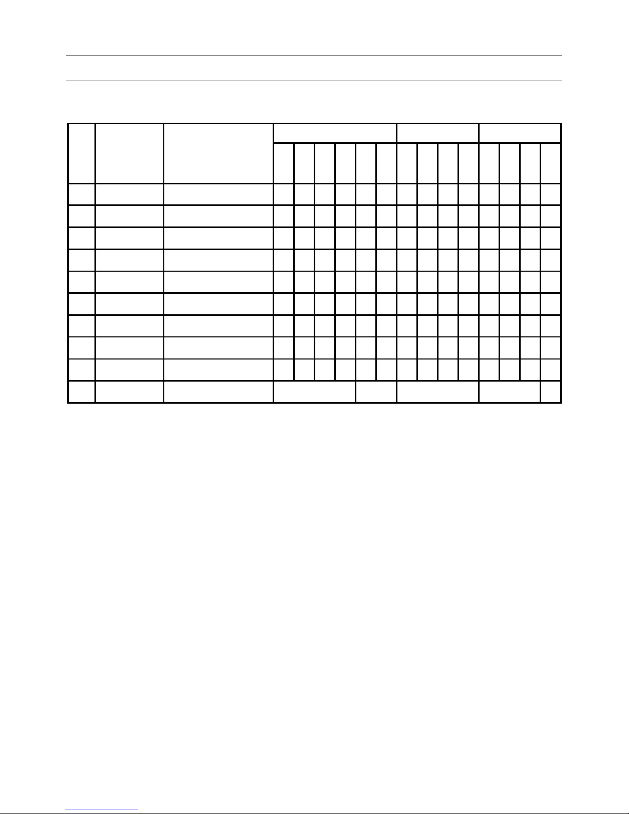
MATERIAL ANALYSIS & TEST RESULTS 5.2.
Homogenous material information according to IPC-1752 standard
No.
Item
Component
Name
Sub Item
Material
Name
RoHS
Halogen
Phthalates
Pb
Cd
Hg
Cr+6
PBB
PBDE F CI
Br I BBP
DBP
DEHP
DINP
1
Resonator
Quartz Crystal
nd
nd
nd
nd
nd
nd
nd
nd
nd
nd
nd
nd
nd
nd
2
Electrodes
Cr+Au
nd
nd
nd
nd
nd
nd
nd
nd
nd
nd
nd
nd
nd
nd
3
Housing
Ceramic
nd
nd
nd
nd
nd
nd
nd
nd
nd
nd
nd
nd
nd
nd 4 Lid
Ceramic Lid & Plating
nd
nd
nd
nd
nd
nd
nd
nd
nd
nd
nd
nd
nd
nd 5 Seal
Solder Preform
nd
nd
nd
nd
nd
nd
nd
nd
nd
nd
nd
nd
nd
nd
6
Terminations
Int. & ext. terminals
nd
nd
nd
nd
nd
nd
nd
nd
nd
nd
nd
nd
nd
nd
7
Resonator
attach
Gold bumps
nd
nd
nd
nd
nd
nd
nd
nd
nd
nd
nd
nd
nd
nd
8
CMOS IC
Silicon & Die pad plating
nd
nd
nd
nd
nd
nd
nd
nd
nd
nd
nd
nd
nd
nd 9 Die attach
Gold bumps
nd
nd
nd
nd
nd
nd
nd
nd
nd
nd
nd
nd
nd
nd MDL
Measurement Detection
Limit
2 ppm
5 ppm
50 ppm
0.003%
0.01%
nd = not detectable
Test methods:
RoHS Test method with reference to IEC 62321-5: 2013 MDL: 2 ppm (PBB / PBDE: 5 ppm)
Halogen Test method with reference to BS EN 14582:2007 MDL: 50 ppm
Phthalates Test method with reference to EN 14372 MDL: 0.003 % (DINP 0.01%)
Page 14

Micro Crystal
Low Power Clock Oscillator 32.768 kHz OV-7605-C8
June 2017 14/20 Rev. 1.0
RECYCLING MATERIAL INFORMATION 5.3.
Recycling material information according to IPC-1752 standard.
Element weight is accumulated and referenced to the unit weight of 6.01 mg.
Item
Material
Name
No.
Item
Component
Name
Material
Weight
Substance
Element
CAS
Number
Comment
(mg)
(%)
Quartz Crystal
1
Resonator
0.22
3.68
SiO2 14808-60-7
Chromium
2
Electrodes
0.0003
0.005
Cr
Cr:
7440-47-3
Ceramic
3 4 Housing
Lid
5.16
85.80
Al2O3 1344-28-1
Gold
2
4
5
6
7
9
Electrodes
Lid
Seal
Terminations
Resonator attach
Die attach
0.20
3.39
Au
Au:
7440-57-5
Tin 5 Seal
0.036
0.60
Sn
Sn:
7440-31-5
Nickel
4 6 Lid
Terminations
0.065
1.07
Ni
Ni:
7440-02-0
Tungsten
6
Terminations
0.24
4.00
W
W:
7440-33-7
Silicon
8a
CMOS IC
0.086
1.43
Si
Si:
7440-21-3
Aluminum
8b
CMOS IC
0.0018
0.029
Al
Al:
7429-90-5
Unit weight (total)
6.01
100
Page 15

Micro Crystal
Low Power Clock Oscillator 32.768 kHz OV-7605-C8
June 2017 15/20 Rev. 1.0
ENVIRONMENTAL PROPERTIES & ABSOLUTE MAXIMUM RATINGS 5.4.
Package
Description
SON-4
Small Outline Non-leaded (SON), ceramic package with ceramic lid
Parameter
Directive
Conditions
Value
Product weight (total)
6.01 mg
Storage temperature
Store as bare product
-55 to +125°C
Moisture sensitivity level (MSL)
IPC/JEDEC J-STD-020D
MSL1
FIT / MTBF
available on request
Terminal finish:
Ceramic
Tungsten
Nickel
Gold
5 µm
0.5 µm
Page 16

Micro Crystal
Low Power Clock Oscillator 32.768 kHz OV-7605-C8
June 2017 16/20 Rev. 1.0
6. APPLICATION INFORMATION
OPERATING OV-7605-C8 6.1.
OV-7605-C8 MCU
V
DD
GND
GND
CLKOUT
2
V
DD
V
DD
10 nF
1
CLKOE
GPIO
1
A 10 nF decoupling capacitor is recommended close to the device.
2
If CLKOE is HIGH (VDD), the CLKOUT pin drives the square wave of 32.768 kHz. When CLKOE is tied to
Ground, the CLKOUT pin is high impedance (Hi-Z).
Page 17

Micro Crystal
Low Power Clock Oscillator 32.768 kHz OV-7605-C8
June 2017 17/20 Rev. 1.0
SOLDERING INFORMATION 6.2.
Maximum Reflow Conditions in accordance with IPC/JEDEC J-STD-020C “Pb-free”
25
Time
Temperature
T
P
T
L
t
P
t
L
t 25°C to Peak
Ramp-up
ts
Preheat
Tsmin
Critical Zone
TL to T
P
Tsmax
Ramp-down
Temperature Profile
Symbol
Condition
Unit
Average ramp-up rate
(Ts
max
to TP)
3°C / second max
°C / s
Ramp down Rate
T
cool
6°C / second max
°C / s
Time 25°C to Peak Temperature
T
to-peak
8 minutes max
min
Preheat
Temperature min
Ts
min
150
°C
Temperature max
Ts
max
200
°C
Time Ts
min
to Ts
max
ts
60 – 180
sec
Soldering above liquidus
Temperature liquidus
TL
217
°C
Time above liquidus
tL
60 – 150
sec
Peak temperature
Peak Temperature
Tp
260
°C
Time within 5°C of peak temperature
tp
20 – 40
sec
Page 18

Micro Crystal
Low Power Clock Oscillator 32.768 kHz OV-7605-C8
June 2017 18/20 Rev. 1.0
HANDLING PRECAUTIONS FOR MODULES WITH EMBEDDED CRYSTALS 6.3.
The built-in tuning-fork crystal consists of pure Silicon Dioxide in crystalline form. The cavity inside the package is
evacuated and hermetically sealed in order for the crystal blank to function undisturbed from air molecules,
humidity and other influences.
Shock and vibration:
Keep the crystal / module from being exposed to excessive mechanical shock and vibration. Micro Crystal
guarantees that the crystal / module will bear a mechanical shock of 5000 g / 0.3 ms.
The following special situations may generate either shock or vibration:
Multiple PCB panels - Usually at the end of the pick & place process the single PCBs are cut out with a router.
These machines sometimes generate vibrations on the PCB that have a fundamental or harmonic frequency
close to 32.768 kHz. This might cause breakage of crystal blanks due to resonance. Router speed should be
adjusted to avoid resonant vibration.
Ultrasonic cleaning - Avoid cleaning processes using ultrasonic energy. These processes can damages
crystals due to mechanical resonance of the crystal blank.
Overheating, rework high temperature exposure:
Avoid overheating the package. The package is sealed with a seal ring consisting of 80% Gold and 20% Tin. The
eutectic melting temperature of this alloy is at 280°C. Heating the seal ring up to >280°C will cause melting of the
metal seal which then, due to the vacuum, is sucked into the cavity forming an air duct. This happens when using
hot-air-gun set at temperatures >300°C.
Use the following methods for rework:
Use a hot-air- gun set at 270°C.
Use 2 temperature controlled soldering irons, set at 270°C, with special-tips to contact all solder-joints from
both sides of the package at the same time, remove part with tweezers when pad solder is liquid.
Page 19

Micro Crystal
Low Power Clock Oscillator 32.768 kHz OV-7605-C8
June 2017 19/20 Rev. 1.0
7. PACKING & SHIPPING INFORMATION
Reel: 7” = 178 mm
Ø
61
,
5
Ø
178
max. 13
min. 8.4
Ø 13
60
°
60
°
1
,
8
Product Label
32
,
768
kHz
Carrier Tape:
Material: Polycarbonate
Width: 8 mm
Tape Leader and Trailer: Minimum length 300 mm
4
±0,1
2,23
±0,05
1,43
±0,05
2
±0,05
4
±0,1
Ø
1
,
0
+
0
,
25
Ø
1
,
5
+
0
,
1
3,5
±0,05
1,75
±0,1
8
+0,3
0,254
±0,02
0,83
±0,05
-0,1
0,061
Cover Tape
0,315
±0,05
All dimensions are in mm
OV-7605-C8_Tape-drw_20170327
Direction of feed
7605
7605
Cover Tape:
Tape: Polypropylene, 3M™ Universal Cover Tape (UCT)
Adhesive Type: Pressure sensitive, Synthetic Polymer
Thickness: 0.061 mm
Peel Method:
Medial section removal, both lateral stripes remain on carrier
Page 20

Micro Crystal
Low Power Clock Oscillator 32.768 kHz OV-7605-C8
June 2017 20/20 Rev. 1.0
8. COMPLIANCE INFORMATION
Micro Crystal confirms that the standard product Low Power Clock Oscillator OV-7605-C8 is compliant with “EU
RoHS Directive” and “EU REACh Directives”.
Please find the actual Certificate of Conformance for Environmental Regulations on our website:
CoC_Environment_OV&OM-Series.pdf
9. DOCUMENT REVISION HISTORY
Date
Revision #
Revision Details
June 2017
1.0
First release
Information furnished is believed to be accurate and reliable. However, Micro Crystal assumes no
responsibility for the consequences of use of such information nor for any infringement of patents or other
rights of third parties which may result from its use. In accordance with our policy of continuous
development and improvement, Micro Crystal reserves the right to modify specifications mentioned in this
publication without prior notice. This product is not authorized for use as critical component in life support
devices or systems.
Micro Crystal AG
Muehlestrasse 14
CH-2540 Grenchen
Switzerland
Phone +41 32 655 82 82
Fax +41 32 655 82 83
sales@microcrystal.com
www.microcrystal.com
 Loading...