

Page 1
!
I
&
i
!Wi
!i!i!
!
a
#
iw
TROUBLE-SHOOTING
GUIDE
1
il
i
I
A-n
Page 2

Configuration
1„
CRT
System
The
the
setting
1-1
14-inch
AC
100V
/
innr
AC
200V
configuration
system
following.
display
color
Transistor
CRT
I
using
amplifier
oo
MAZATROL
Control
cp
/
unit
¥
r
M-32A
generally
is
composed
Portable
reader
tape
Puncher
Printer
of
$
1
I
J
!
L
k
L_
a
d
a
Encoder
4-axis
motor
Z-axis
motor
rn
r“-
if-axis
1
motor
—
X“2
X-axis
motor
J
P
=3
Z3
Spindle
[9j
Manual
generator
rotary
Control
Pÿfi,
d
pulse
encoder
Power
control
1
---
Limit
__
switch,
reÿ--,
:
l'
__
1
I
j
l
i
Page 3
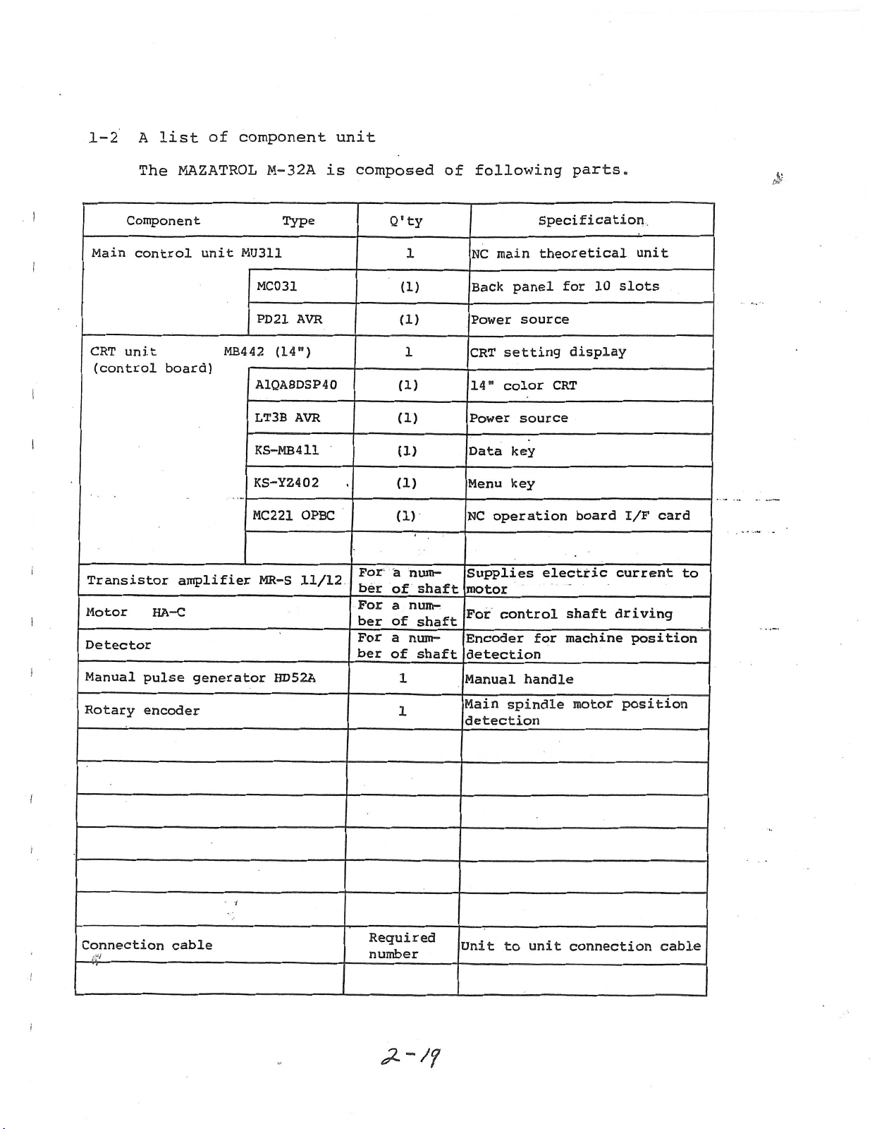
1-2
A
list
component
of
unit
The
Component
Main
CRT
(control
Transistor
Motor
Detector
Manual
control
unit
HA-C
pulse
MAZATROL
unit
MB442
board)
amplifier
generator
M-32A
Type
MU311
MC031
PD21
AVR
(14")
A1QA8DSP40
LT3B
AVR
KS-MB411
KS-YZ402
MC221
MR-S
HD52A
is
OPBC
11/12
composed
Q'ty
1
(1)
(1)
1
(1)
(1)
(1)
(1)
(1)
For
a
num¬
ber
of
shaft
For
a
num¬
ber
of
shaft
For
a
num¬
ber
of
shaft
1
following
of
NC
Back
Power
CRT
14"
Power
Data
Menu
operation
NC
Supplies
motor
For
Encoder
detection
Manual
Specification
theoretical
main
panel
for
source
setting
color
CRT
source
key
key
electric
control
shaft
machine
for
handle
parts,
slots
10
display
board
current
driving
unit
card
I/F
position
£
to
Main
Rotary
Connection
i
encoder
cable
1
Required
number
Unit
spindle
detection
unit
to
motor
connection
position
cable
Page 4
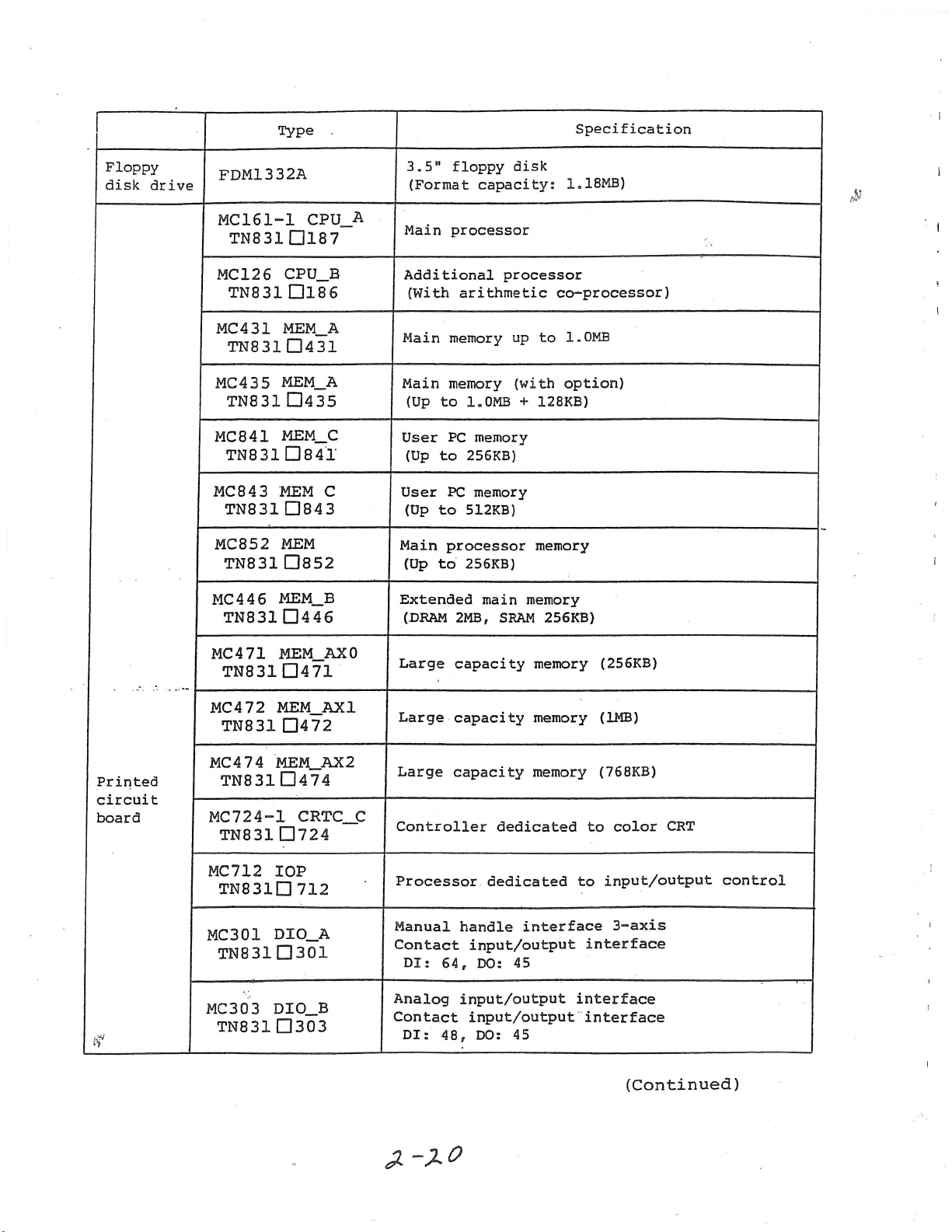
Type
Specification
I
Floppy
disk
drive
FDM1332A
MC161-1
TN831
MC126
CPU_B
TN831
MC431
TN831
MC435
TN831
MC841
TN831
MC843
TN831
MC852
TN831
MC446
TN831
MEM_A
CU431
MEM_A
D435
MEM_C
111841'
MEM
D843
MEM
0852
MEM_B
D446
CPU_A
Q187
Q186
3.5"
floppy
(Format
processor
Main
Additional
(With
Main
Main
(Up
User
(Up
C
User
(Up
Main
(Up
Extended
(.DRAM
arithmetic
memory
memory
to
1.0MB
PC
to
256KB)
PC
to
512KB)
processor
256KB)
to
2MB,
disk
capacity:
processor
up
to
(with
+
128KB)
memory
memory
memory
memory
main
256KB)
SRAM
1.18MB)
co-processor)
1.0MB
option)
i
$
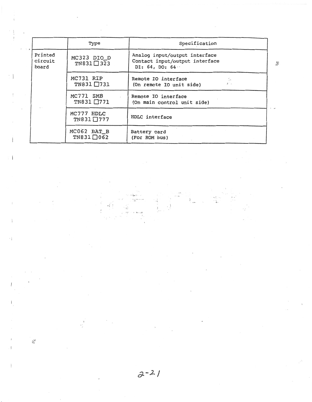
Printed
circuit
board
MC471
TN831
MC472
TN831
MC474
TN831
MC724-1
TN831
MC712
TN831D
MC301
1
3
8
TN
MC303
TN831
MEM_AX
D471
MEM_AXl
Q472
MEM_AX2
A
OAl
CRTC_C
0724
I0P
712
_
A
DIO
1
3
0
DI0_B
D303
0
Large
Large
Large
Controller
capacity
capacity
capacity
Processor
Manual
Contact
DI:
Analog
Contact
DI:
handle
input/output
64,
DO:
input/output
input/output
DO:
48,
memory
memory
memory
dedicated
dedicated
interface
45
45
(256KB)
(1MB)
(768KB)
color
to
input/output
to
3-axis
interface
interface
interface
(Continued)
CRT
i
control
JL-XO
Page 5
I
!
Type
Printed
circuit
board
MC323
TN
MC731
TN831
[
MC771
TN831
MC777
TN831
MC062
TN831
3
8
DIO_D
1
3
RIP
D731
SMB
D771
HDLC
D777
BAT_B
D062
2
3
Analog
Contact
64,
DI:
Remote
(On
remote
Remote
(On
main
HDLC
interface
Battery
ROM
(For
input/output
input/output
DO:
10
interface
10
10
interface
control
card
bus)
Specification
interface
interface
64
side)
unit
side)
unit
£
!
I
Page 6

1-3
Hardware
MASTER
RS-232C
"
14“
color
SlffiS
TtT
(
LEJI
RS-232C
.
\
—
E
nicro
3.3"
floppy
dial
drive
configuration
CONTROL
MC161-1
CPU.A
Serial
\\
input/
output
«"T
l
<c
MC852
<
\
)
}
<
1
>
1
i
MEM
Syotoa
MC841/
843
MEM_C
FC
MC
CRTC
toeBory
14"
-
724-1
C
color
»ry
CRT
1
l
l
$
MC
Nr
Hi
J—
r—
IOP
Input/
•
prccoBBor
712
output
!
l
X
/
)
>
1
>
>
i
X
/
MC
771
SMB
v.
at
I/O
interface
UNIT
DSP
CPU
MC431/435
MEM_A
eataory
Main
(POM)
controller
ZzL
/
/
/
/
/
X
/
/
/
/
1/
/
/
/
/
/
/
%
/
/
/
/
/
ZZZ/ZZ2
X
A
/
/
/
/
/
s//V"/
7/777
/
/
/
/
/
/
/
/
y
rfn
-a
CPU
iSyntea
I
I
I
MC
471
MEM_AX0/
capacity
Lar$e
Estons&od
capacity
MC446
MEM_B
Entcmdod
Pcs*er
interface
Ptwer
interface
I
Pe*er
interface
f
MC126
CPU_B
Serial
input/
output
EL
MC777
HDLC
Optical
interface
/MC
472
AX1
TT
474
MC
MEM__AX2
~
larÿe
y
tsssory
MC323
DIO
Anput/cutput
MC
DIO
input/
output
_
MC
DIO
Arput/output
D
301
A
303
B
I
Nx
ID
RS232C
i
OPTICAL
£
)
X
i
\
l
l
/
X
/
i
X
i
!
i
Spindle
encoder
Servo
acplif
iar
P
-
O
*
o
i
X
7*
FIBER
mr
I»-or
control
f»S®»
...
m&m
>
O
O
/•
•;
J'..
Vv,
.
«
'v
!
J
-X
o
f
&
A.-2Z
/////
/
/
/
/
/
/
/
REMOTE
1
MC
73
RIP
Bsassta
I/O
press
occc
l
T
UNIT
IO
l
*
!
Page 7

Printed
(including
circuit
board
optional
10
standard
accommodation
specifications)
A
3
2
M
-
98
76
54
32
diagram
$
1
External
04
to
o
'O
2
view
«L
of
CM
o-
U
2
5
CO
u
2
\
s
2
-f
LO
co
U
2
\
CO
u
2
main
2
«N1
in
oo
o
£
+
to
u
C'-
c
c-
U
2
+
to
04
CJ
2
to
-*r
u
2
—
\
to
**r
u
2
unit
.
o
S
+
04
Xr~
O
2
\
04
t-
O
s
\
'ts4
o
I
oo
o-
2
'MV
tÿ-
u
X
X
co
U
2
Oi
>
<
o
04
co
X
X
X
X
CO
U
2
X
X
co
co
U
U
2
2
j
n
S
s]
i
I
Si
•4&i:
i
p
t
<3
I--1
ffi
y
iS
i
in
is:
i
rm
&
1
•-••ft
-i
f
.
•
T
&
T
V*;
•
•:
i
4--.'
it
wr
&
•
r
SSI
*
II
gss
l
HR
•
>
#;,%
BQ
•=£:
I
sea
*1
a*
t
Hi
ill
!i
£
i
'
9
m
m
R
*
B
1
*.7V
4k.
i*
%
e
%
£
WMMp
a
i
Hi'
4.
l
M-
A
2
3
J-~z3
Page 8

3-2
3-2-1
fL
S
2
List
M-32A
LEDl
LED2
1
©LED3
22
a
s
U-
re
ac
U
2
+
£
rr
ce
*3
2
of
10
®D.AL
®LED1
©LED2
©LED3
®WD0G
®D.WD
CM
in
oo
s
+
3
2
LEDs
9
®LED1
©LED2
©LED3
®WDOC
2
+
to
CM
£
of
8
©LEDl
®LED2
®LED3
©LEW
©LED5
VD
3
s
\
I
to
2
each
7
+
CM
\
CM
**r
\
£
u
2
L
6
card
5
5
2
(unit)
3
<
£-
2
5
ce
ro
D
2
2
2
>3
r?
!
$
7
7
©LEDl
©LED2
os
>
<
re
U
2
©LED3
tÿ-
.<t
1
©LEDl
LED2
LED3
CM
3
2
;ÿ
KyLDG
*i..
l.KDl
ro
re
o
CM
3
0
2
-
I
i
>
i
-i
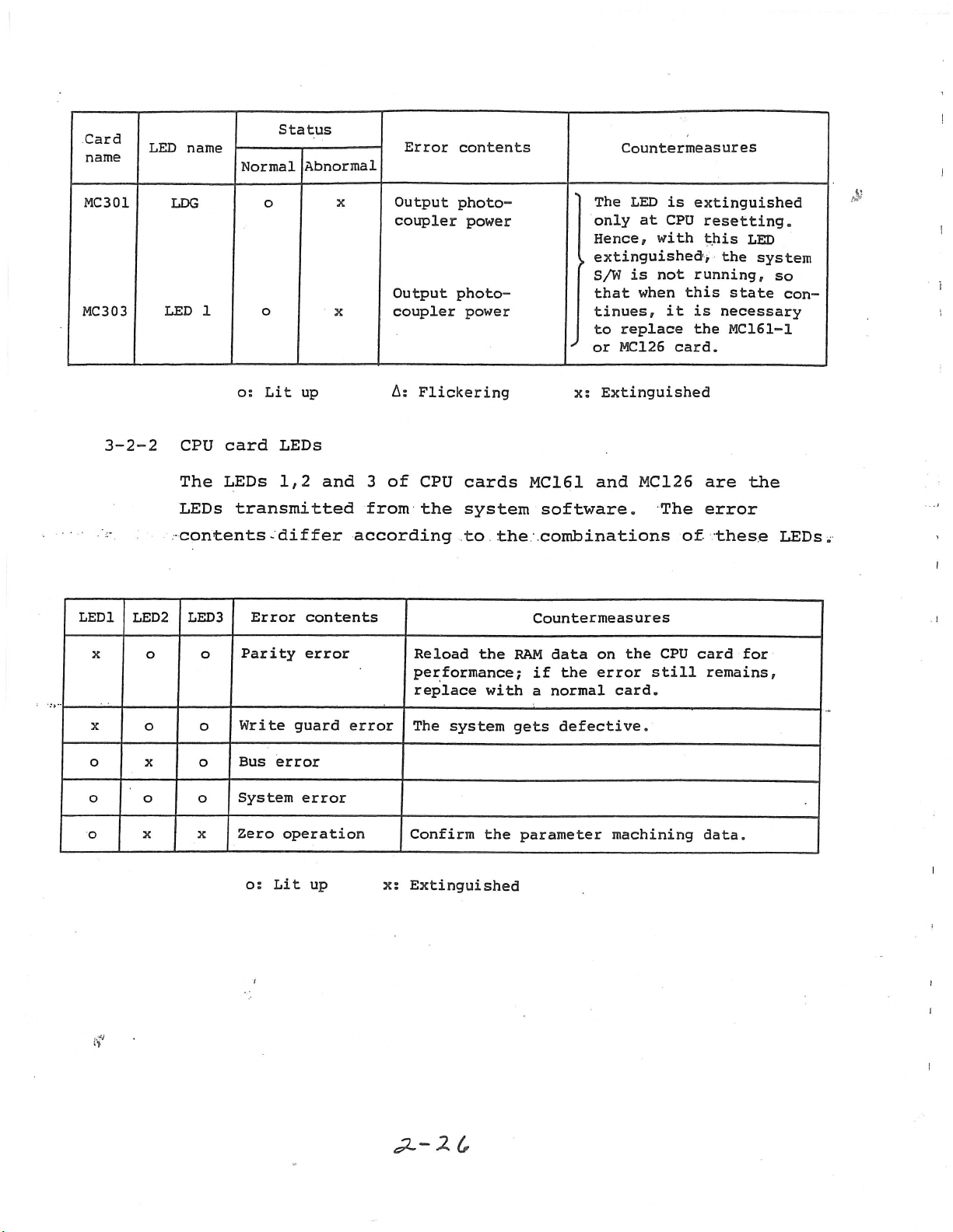
Card
name
MC712
MC161
-1
iii
LED
LEDl
LED
LED
LEDl
LED
LED
WDOG
name
2
3
2
3
Status
Normal
X
o/A
o/A
x
A
A
x
Abnormal
o
x
x
o
Error
contents
System
System
System
>
Watchdog
alarm
ready
ready
alarm
Countermeasures
Normally
only
izing
the
constantly,
normal
A
B
Replace
when
guish
the
side
this
at
after
LED
resetting,
remains
time
the
replace
card.
MC712
the
and
LEDl
simultaneously,
when
card
LED
MC201
of
lit
LED2
on
only
2
initial¬
if
up
a
with
card
extin¬
and
board
extin¬
i
up
lit
is
LED
guishes.
;
The
differ
>
nation.
Refer
Replace
to
the
a
of
item
normal
contents
due
to
with
error
the
may
combi¬
3-3-5.
I
card.
I
(Continued)
£-2*/
Page 9

I
Card
name
MC126
LED
D.
D.
LED1
LED
LED
WDOG
name
AL
WD
2
3
Status
Normal
x
x
x
o
O
x
Abnormal
o
o
o
Error
DSP
alarm
DSP
watchdog
Watchdog
contents
alarm
alarm
Countermeasures
Check
nector
After
age
lamp
the
The
differ
.
nation.
J
item
Replace
the
that
is
connected.
checking
the
due
Refer
cable,
with
to
a
of
lights
card
contents
3-3-5.
with
CAM11
the
replace
up,
good
a
of
error
the
to
normal
con¬
break¬
if
the
one.
may
combi¬
the
card
£
I
MC446
I
LED1
LED
LED
2
3
x
x
x
o
o
o
DRAM
SRAM
DRAM
alarm
parity
parity
battery
error
error
Reload
performance,
LED
place
Charge
battery.
the
still
with
or
data
and
lights
a
normal
replace
again
if
up,
the
for
the
re¬
card.
LED4
5
LED
MC471
l
MC472
LEDl
LED
LED3
LEDl
LED
LED
2
2
3
t?
x
x
x
x
x
x
k
x
o
o
o
o
o
o
o
o
SRAM
battery
alarm
i
1
Memory
Parity
Memory
Battery
Parity
Memory
Battery
guard
error
guard
alarm
error
guard
alarm
error
error
error
Charge
battery,
machining
The
system
Reload
performance,
still
LED
place
The
system
Charge
battery,
machining
Reload
or
the
with
or
and
the
replace
and
data.
gets
data
lights
a
gets
replace
data.
data
performance,
still
with
The
Charge
battery,
machining
lights
a
normal
system
or
and
gets
replace
data.
the
reconfirm
defective.
again
and
normal
if
up,
for
the
re¬
card.
defective.
the
reconfirm
and
up,
again
replace
if
for
the
card.
defective.
the
reconfirm
the
the
LED
the
I
-2
A
S'
(Continued)
Page 10
Card
name
LED
name
Status
Normal
Abnormal
Error
contents
Countermeasures
MC301
MC303
3-2-2
LED1
LDG
1
LED
CPU
The
LEDs
LED2LED
o
o
os
Lit
up
card
LEDs
LEDs
1,2
transmitted
-differ
3
Error
contents
x
X
and
3
from
according
Output
coupler
Output
coupler
A;
Flickering
of
CPU
the
photo¬
power
photo¬
power
cards
system
to
the
The
LED
at
only
Hence,
extinguished,
(
S/W
that
tinues,
to
or
x;
Extinguished
MC161
and
software.
with
not
is
when
replace
MC126
MC126
The
.combinations
Countermeasures
is
extinguished
CPU
resetting.
this
the
running,
this
state
it
is
necessary
the
MC161-1
card.
are
error
of
these
£
LED
system
so
con¬
the
LEDs.
Parity
x
x
o
o
o
o
o o
x
o
x
o
o
o
X
Write
Bus
error
System
Zero
o;
Lit
i
error
guard
error
error
operation
up
Reload
performance;
replace
The
system
Confirm
xs
Extinguished
the
with
the
data
RAM
the
if
a
normal
defective.
gets
parameter
on
error
machining
the
still
card.
CPU
card
for
remains,
data.
I
I
I
2.
(#
Page 11
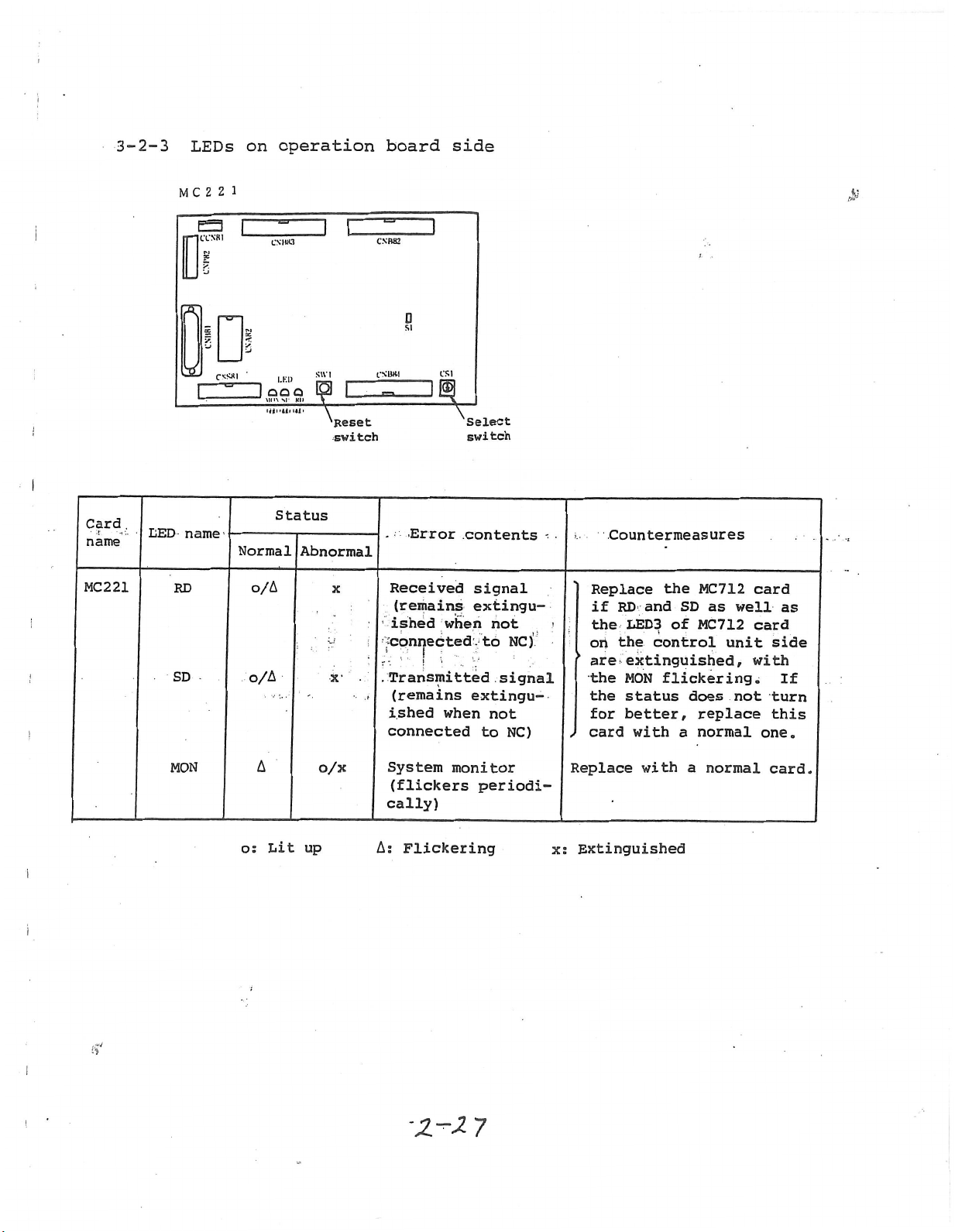
3-2-3
LEDs
c
M
on
operation
l
2
2
board
side
$
I
!
E3
T-ICCN81
CXHH3
]
[
CNB82
]
us
si
|Q
CNS><|
.
[
I
Card
name
MC221
LED
name-
RD
QQQ
Ml
-iii-U-itf-
Normal
o/A
SVV
I.KI)
IP
>\
SI-
Kll
Status
Abnormal
I
\
Reset
switch
x
u
CN
138-1
Received
(remains
ished
/connected
r
SD
o/A
x
.Transmitted
(remains
ished
connected
Error
'
!
CSl
Select
switch
contents
signal
extingu¬
when
.to
i
extingu¬
when
not
signal
not
to
NC)
NC)
•
!
.Countermeasures
the
Replace
if
RD
the
the
on
’
are
the
the
for
card
and
LED3
control
extinguished,
MON
status
better,
with
MC712
SD
of
MC712
t
flickering.
does
replace
a
normal
as
well
card
unit
with
not
card
as
side
If
turn
this
one.
System
(flickers
cally)
As
Flickering
monitor
periodi¬
Replace
Extinguished
x:
with
a
normal
card.
o:
A
Lit
o/x
up
MON
I
!?
7
Page 12

3-3
Likely
|WDOG|
1.
(1)
"With
causes
Watching
CPU-A
WDOG
of
alarm
error
,
CPU-B
WDOG
lit
$
up
Missetting
rH
r—
I
to
CO
Q
Q
CQ
<
D
D
Pg
a*
u
o
U4
14-1
o
o
cn
cn
c
c
-H
-H
4J
4-3
JJ
4J
03 03
c/3
w
c/3
w
-H
-H
2
2
2
•H
4->
*P4
s
CL,
u
C
03
C/3
U3
<
D
CU
U
03
>
•H
4->
U
(U
03
Q
-H
Q
CQ
D
PH
U
4J
03
03
>
O
03
Watchdog
<
I
§
s
U-l
O
C
-2
-U
O
3
M
M
0)
a
error
C/3
U
-S
B
to
U
ro
Q,
m
I
s
W
s
Tl
c
ro
Memory
concerned
c
ro
C/3
1
f
03
2
-H
W
L4
2
03
4J
03
4-3
>
4J
CQ
U
03
I
4-J
X
C£)
03
Q
2
c
(13
f
2
§
03
>
4J
U
03
u-i
03
Q
T3
(0
°
CQ
s
W
2
„
14
I
§
•H
JJ
a!
C
»H
03
>
*H
4J
U
03
44
03
a
44
n3
C/3
M
03
U
o
1
if
"Watchdog
The
properly
of
bringing
such
as
formed,
run
passes
normally
system
to
through
a
lock
of
terminal
put
thus
take
urgent
Error",
order
in
the
NC,
running
with
a
through
the
routine,
a
constant
of
the
obtained
and
occurring
assure
to
at
to
real
counter
system
specific
the
some
to
due
and
the
frequency
counter,
the
interrupts
appropriate
when
the
safety
an
immediate
time,
a
getting
routine.
reason,
counter
provided
is
counter
the
CPU,
measures.
system
the
system,
of
stop.
periodical
reset
Should
the
does
the
system
not
to
overflows,
making
it
fails
is
a
In
system
routine
every
system
can
not
get
reset.
the
clock
and
possible
to
capable
is
time
fails
pass
out-
the
run
the
If
to
Page 13

(2)
With
D.
WD
lit
up
Watchdog
A'
error
'
The
-
(servo
error
occurs
in
when
watchdog'
system)
of
the
when
less
MCU
than
main
Trouble
04
w
a
>
x>
2
44
D
error
total
1
servo
a
certain
processing
of
against
system.
MCU
in
5
B3
°
n
04
o
E
u
c
•o
•»
H
c
<0
5
U
H3
MCP'
.
processing
the
time
falls
is
the
watchdog
The
period
§
u
-H
O
-U
4-1
M
U
flJ
<D
V)
C
c
c
T4
O
o
Q>
PH
>
?5
0)
u
44
d)
44
Q
O
watchdog
error
watchdog
can
not
(normally
behind
be
the
error
of
CPU
error
carried
1.7
time.
of
of
as
ms)
MCU
an
DSP
out
or
Page 14
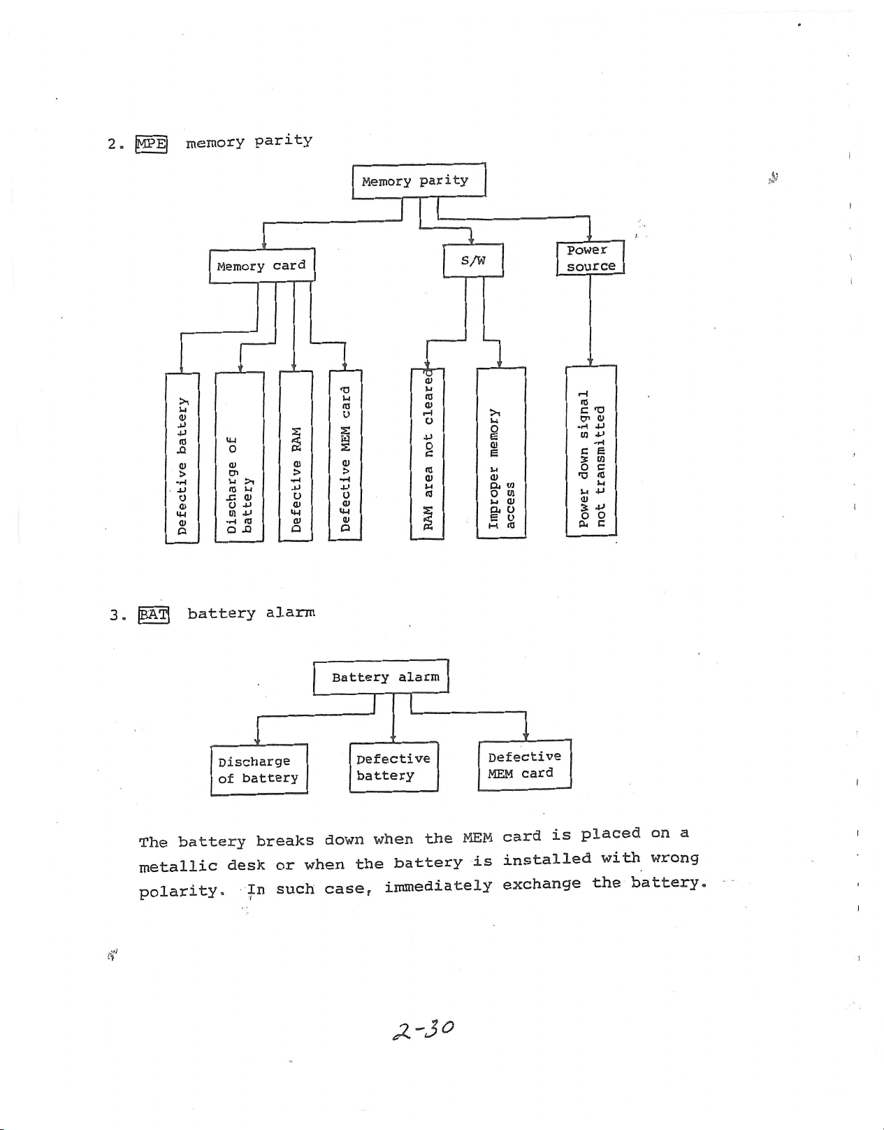
[MPEl
2.
memory
parity
I
>i
<5
4J
ra
JQ
Q)
>
-H
u
QJ
U-I
QJ
Q
Memory
u-i
o
QJ
cn
U
>i
Q3
M
0)
JC
OJ
U
in
ra
•H
Q
xi
card
OJ
4J
u
<D
U-|
QJ
a
T5
£
s
w
2
>
-H
o
U-4
D
u
QJ
QJ
QJ
Memory
parity
s/w
-’tr
QJ
IQ
GJ
rH
o
4J
0
C
ra
QJ
ra
1
n
o
E
QJ
E
u
QJ
a
o
u
Du
E
M
in
in
QJ
O
O
ra
Power
source
ra
T3
C
0>
CP
4J
-H
J->
in
-H
c
E
in
£
c
O
ra
TJ
uiJ
QJ
4J
5
o
o
c
PU
$
i
i
i
)
pAlj
3
o
The
metallic
polarity.
if
battery
Discharge
of
battery
desk
alarm
battery
breaks
or
such
In
Battery
down
when
case,
alarm
Defective
battery
when
the
the
battery
immediately
Defective
card
MEM
card
MEM
installed
is
exchange
is
placed
with
battery.
the
a
on
wrong
i
I
1
Page 15

3-4
Inspection
procedures
for
troubles
(1)
Confirmation
Confirmation
3-phase
The
no-fuse
no-fuse
voltage
I
breaker
breaker,,
is
of
power
input
of
input
terminals
applied
A
\
©
||
R
power
Hence,
to
©
©
1|
S
T
ON
voltage
power
voltage
R.S.T.
make
R.S.T.
Input
voltage
supplied
is
through
sure
terminals.
that
to
the
specified
the
NC
the
machine
$
side
side
_____
P
OFF
W
V
U
©
©8
©B
v
v
V
Output
To
transformer
The
single-phase
.....
minal
sure
fied
f
stand
that
voltage
•
the
of
of
the
terminal
AC100V
input
DC
voltage
power
stand
±15%.
PD21
is
is
connected
of
control
applied
with
to
the
unit.
the
ter-
•
Make
speci¬
X-3
/
Page 16
!
:
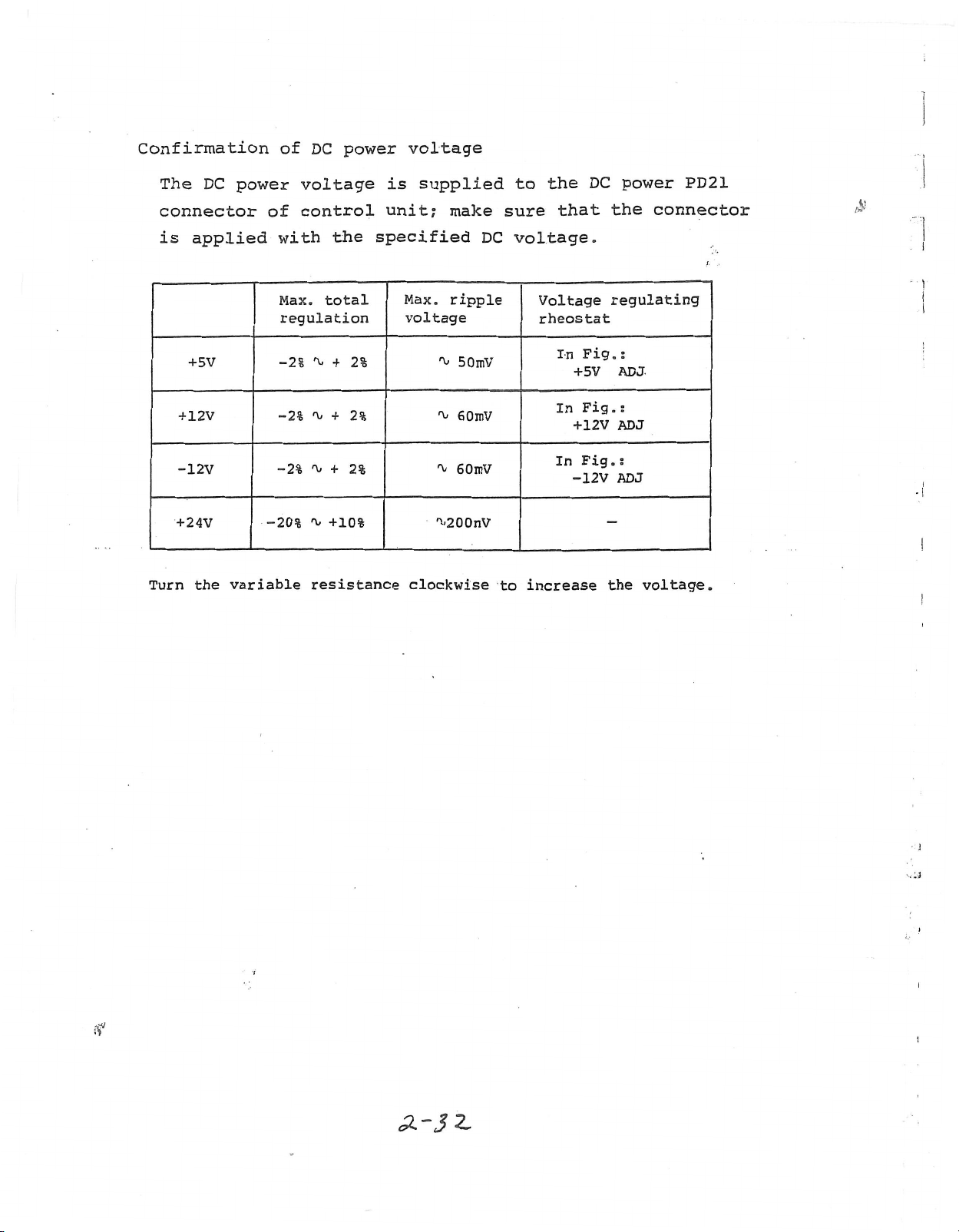
Confirmation
power
DC
The
connector
is
applied
+5V
+12V
-12V
+
24V
the
Turn
of
-20%
variable
of
DC
power
voltage
control
with
Max.
regulation
-2%
-2%
-2%
the
total
+
2%
+
2%
%
+
2%
+10%
resistance
voltage
is
supplied
unit;
make
specified
Max.
ripple
voltage
v
50mV
60mV
60mV
r'j200nV
clockwise
to
sure
voltage.
DC
to
DC
the
that
Voltage
rheostat
Fig
In
+5V
Fig.:
In
+12V
Fig.
In
-12V
increase
power
the
PD21
connector
regulating
:
.
ADJ
ADJ
:
ADJ
voltage.
the
£
)
i
if
J
•.
Li
I
Page 17
i
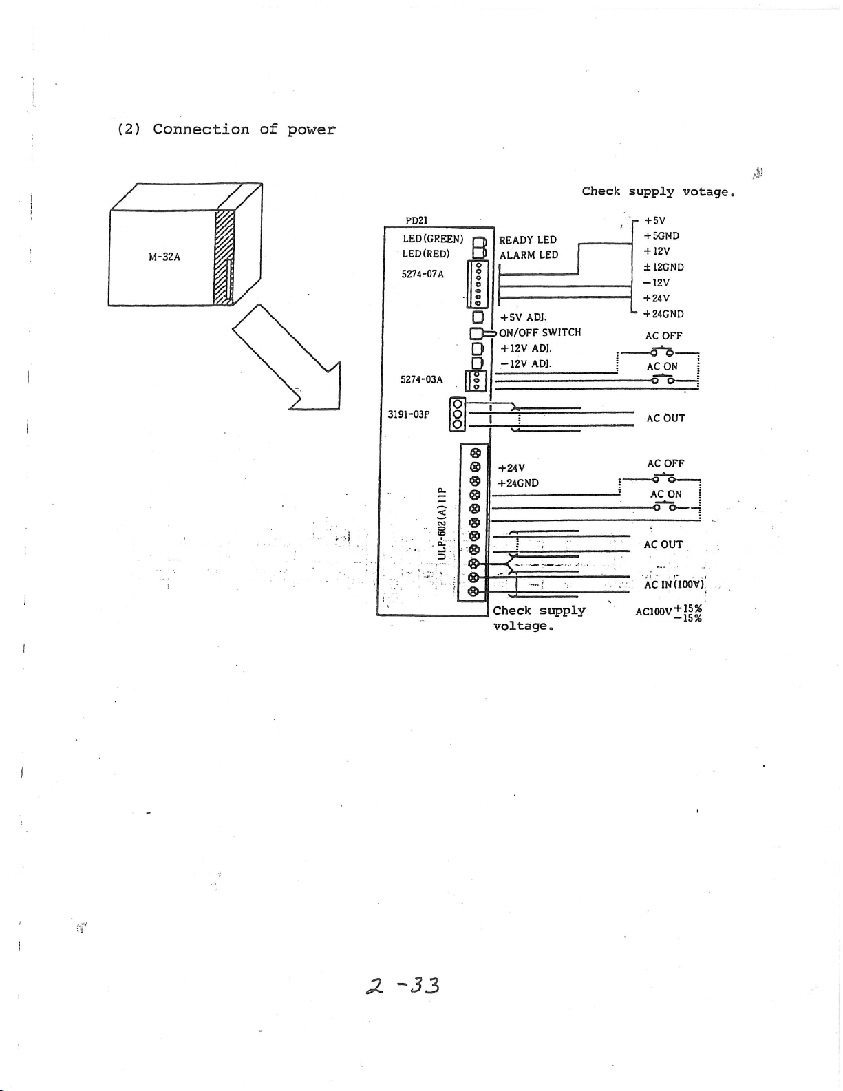
(2)
Connection
of
power
£
Check
PD21
(GREEN)
;
M-32A
i
LED
LED
5274
(RED)
-07
A
B
o
§
s
o
Q=>
Q
D
-03A
5274
3191-03P
HI
I
Cu
©
>
i
V
i
©
READY
ALARM
+5V
ADJ.
ON/OFF
12V
+
-12V
"Xr
I
-f
V
24
+24GND
!
LED
LED
SWITCH
ADJ.
ADJ.
supply
/
r
-
!
+5V
5GND
+
12V
+
12GND
±
-12V
24V
+
+24GND
AC
OFF
cT-6
-
AC
ON
•o
AC
OUT
AC
OFF
AC
ON
-oÿo
AC
OUT
votage„
:
|
.
:
—
—
_
!
$
l
©ÿ
-f
Check
voltage
supply
.
ACINUOOV)
+
ACIQOV
Jf*
lb
—
t
%
X
33
-
Page 18

x
i
I
u
L.
11
Device
XO
XI
T2
X3
X4
X5
X6
X7
Device
X10
Xll
X12
X13
X14
X15
X16
X17
Device
X20
X21
X22
X23
X24
X25
X26
X27
Device
X30
X31
X32
X33
X34
X35
uxg
j.
ua
u
m
X
x
Abbreviation
Abbreviation
Abbreviation
Abbreviation
G
uxu
u
a
a
Signal
Signal
•
Signal
*Stroke
*Stroke
*Stroke
Signal
\
end
end
end
end
J-
"T
I
name
name
-1
-2
-3
-4
atop
/
name
name
j»
a
JL
h.
L.
a.
u
ca
v-
CHD
12-36
4
-
rrz
37
-
I
23
-
38
-
6
-
CHD
12-26
42
10
27
43
11
28
44
CHD
12-47
15
32
48
16
49
17
50
CHD
11-10
17
4
11
18
5
Device
X8
X9
XA
XB
XC
XD
XE
XF
Device
X18
X19
XU
X1B
X1C
X1D
X1E
X1F
Device
X28
X29
X2A
X2D
X2C
X2D
X2E
F
2
X
Device
X38
X39
X3A
X3D
X3C
X3D
Abbreviation
Abbreviation
near
near
near
*Reference
near
Abbreviation
*Stroke
*Stroke
*Stroke
t
la
Abbrev
ion
Signal
Signal
point
point
point
point
Signal
end
end
end
end
Signal
laoie
name
name
poation
detection
poation
detection
poation
detection
poation
detection
+1
+2
return
1
return
2
return
3
return
4
name
+3
+4
name
“
M
i.
1
-
CHD
12-
1
19
34
2
20
35
3
21
CHD
12-24
39
7
25
40
8
41
9
CHD
12-12
29
45
13
30
46
•14
31
CHD
11-14
U)
u
o
g
u>
u>
Ln
3:
H
g
>
n
w
H
t-1
M
g
b
&
KJ
o
H
t
U)
SJ
o
.
u»
U)
o
Page 19

X36
X37
12l
I
19
X3E
X3F
16
3
c
i
too
Note
Is
The
signals
marked
*
are
handled
at
contact
D
•
:
.
k
<6
i
7
circuits.
l
•
•*.
t
u
P
Ui
o
V.
g
vs
B
L
i
;
D
U5
Ln
PC
s
o
w
c
P
w
Li
N
C
P
M
U
u
c
?
B
e
Page 20

Input
Signal
from
Machine
(2/A)
Second
card
Table
4-jl-z
I
u
Device
XAO
XA1
XA2
XA3
XAA
XA5
XA6
XA7
Device
X50
X51
X52
X53
X5A
X55
X56
X57
Device
X60
X61
X62
X63
X6A
X65
X66
X67
Device
X70
X71
2
X7
X73
X7A
X75
X76
Abbreviation
Abbreviation
Abbreviation
’“'Stroke
Abbreviation
Signal
Signal
Signal
end
end
Signal
name
name
name
-5
-6
name
CMD
-36
22
37
23
38
CMD
-26
A2
10
27
A3
11
28
CMD
-A
15
CMD
-10
)evice
XA8
A
5
6
Device
AA
Device
7
32
A8
16
A9
17
50
Device
17
A
11
18
5
12
XA9
XAA
XAB
XAC
XAD
XAE
XAF
X58
X59
X5A
X5B
X5C
X5D
X5E
X5F
X68
X69
X6A
X6B
X6C
X6D
X6E
X6F
X78
X79
X7A
X7B
X7C
X7D
X7E
Abbreviation
Abbreviation
*Reference
near
near
Abbreviation
Abbreviation
Signal
Signal
point
point
Signal
end
end
Signal
name
name
poation
detection
poation
detection
+5
+6
return
return
name
name
5
6
CMD
1
-
19
3A
2
20
35
3
21
CMD
-2A
39
7
25
AO
i
8
Al
9
CUD
-12
29
A5
13
30
A6
.
1A
31
CMD
U)
to
o
g
UJ
LO
Ln
-1A
1
8
15
2
9
16
§
>
n
M
H
£
%
G
Page 21

X77
19
X7F
3
(
h
NJ
Note
Note
)
Is
2:
••
The
DI
•
for
X70
marked
X7F
-
i
are
*
exists
handled
only
in
at
DIO-A
contact
B
or
!
•
a
i.
r
•
!
DIO-D
4
i
signals
circuits.
card.
to
U)
o
§
w
(jj
Ul
s:
s
8
%
O
g
M
Page 22

>0
l
IA/
Device
X100
X101
X102
X103
X104
X105
X106
X107
Device
X110
Xlll
X112
X113
X114
X115
X116
X117
Device
X120
X121
X122
X123
X124
X125
2
6
Xl
Xlz7
Device
X130
X131
X132
X133
X134
X135
X136
X137
Note
Note
Abbreviation
34
Abbreviation
Abbreviation
Abbreviation
1:
2:
X108
reaet
X127
ia
signal
ia
Signal
Signal
Signal
*
Emergency
Signal
the
fixed
of
CNC
set
to
at
1
name
name
name
stop
name
device
input
emergency
number
user
on
stop.
CMD
82-36
82-26
22
37
23
38
CMD
42
Device
X108
4
X109
X10A
X10B
X10C
5
X10D
X10E
X10F
6
Device
X118
X119
10
27
43
11
28
44
CMD
Device
82-47
15
32
40
11
49
17
50
CMD
81-10
assigned
PLC.
Device
17
4
11
18
5
12
19
X11A
X11B
X11C
X11D
X11E
X11F
X128
X129
X12A
X12B
X12C
X12D
X12E
X12F
X138
X139
X13A
X13D
X13C
X13D
X13E
X13F
to
Abbreviation
Abbreviation
Abbreviation
Abbreviation
NC
reset.
Do
NC
sure
Signal
reset
Signal
to
Signal
Signal
assign
name
name
name
name
it
to
the
CMD.
82-
19
34
20
35
CMD
82-24
CMD
82-12
'
CMD
81-14
NC
1
2
3
21
39
7
25
40
8
41
9
29
45
to
a:
U)
’TJ
'
1
o
§
U)
to
Ln
X
H
3
%
>
n
w
H
3
u>
ro
O
1
7*
LJ
M
O
X
Ui
LAJ
o
x
K
uV
Y-
Page 23

Vi
a
Device
XIAO
X1A1
X1A2
X1A3
X1AA
X1A5
X1A6
X1A7
Device
X150
X151
X152
X153
X15A
X155
X156
X157
Device
Abbreviation
Abbreviation
Abbreviation
Signal
Signal
Signal
name
name
name
Device
Device
>
f
•
-
XIAO
X1A9
X1AA
X1AB
X1AC
X1AD
X1AE
X1AF
X158
ns?
5
XI
A
X15D
X15C
X15D
X15E
X15F
Device
Abbreviation
Abbreviation
Abbreviation
Signal
Signal
Signal
name
name
name
Device
Abbreviation
Signal
name
Device
Abbreviation
Signal
name
L*3
UJ
O
g
LJ
U)
Ln
EC
H
£>
n
w
H
G
i
i
[
l
t
l
i.
c
Page 24

Sensor
Device
Device
i
Device
X178
X179
X17A
X17B
X17C
X17D
X17E
X17F
Input
Signal
Table
Abbreviation
(Skip
(Skip
(Skip
(Skip
interrupt
Interrupt
Interrupt
Interrupt
Abbreviation
Abbreviation
(l/l)
Signal
1)
2)
3)
4)
Signal
Signal
>
name
signal
signal
signal
signal
name
name
1
2
3
4
CNA
18-
/
1
)evice
Abbreviation
/
C
J/t
Signal
name
Table
4-4-1
i
CNA
2
5
6
8
9
12
13
CNA
CNA
device
Device
Abbreviation
Abbreviation
Signal
Signal
name
name
CNA
CNA
Device
Abbreviation
Signal
name
CNA
Device
Abbreviation
Signal
name
CNA
u>
to
o
s
Lo
to
Ln
P:
H
rn
n
W
H
£
R
Page 25

%
Device
X180
X181
X182
X183
X184
X185
XI
Abbreviation
RJDY1
RDY2
RDY3
RDY4
RDY5
RDY6
6'
8
-
Servo
Servo
Servo
Servo
Servo
Servo
X187
Device
X190
X191
X192
X193
X194
X195
Abbreviation
MVP1
MVP2
KVP3
MVP4
HVP5
MVP6
Axis
Axis
Axis
Axis
Axis
Axis
X196
i
X197
Device
XIAO
X1A1
X1A2
X1A3
X1A4
X1A5
X1A6
Abbreviation
ZP11
ZP12
ZP13
ZP14
ZP15
ZP16
First
position
Firat
position
First
position
First
position
Firat
position
First
position
X1A7
Device
X1B0
X1B1
Abbreviation
ZP31
ZP32
Third
position
Third
position
Signal
ready
ready
ready
ready
ready
ready
Signal
moving
moving
moving
moving
moving
moving
name
Signal
reference
arrival
reference
arrival
reference
arrival
reference
arrival
reference
arrival
reference
arrival
Signal
reference
arrival
reference
arrival
name
name
name
axis
axis
axis
axis
axis
axis
axis
axis
axis
axis
axis
axis
axis
axis
axis
axis
axis
axis
axis
axis
1
2
3
4
5
6
+1
+2
+3
+4
+5
+6
1
2
3
4
5
6
1
2
Device
X188
X189
X18A
X18B
X18G
X18D
X18E
X18F
Device
X198
X199
X19A
X19B
X19C
X19D
X19E
X19F
Device
X1A8
X1A9
X1AA
X1AB
X1AC
X1AD
X1AE
X1AF
Device
X1B8
X1B9
Abbreviation
AX1
AX2
AX3
AX4
AX5
AX6
Axis
Axis
Axis
Axis
Axis
Axis
Abbreviation
HVM1
MVM2
MVM3
MVM4
MVM5
MVM6
Abbreviation
ZP21
ZP22
ZP23
ZP24
ZP25
ZP26
Abbreviation
ZP41
ZP42
Axis
Axis
Axis
Axis
Axis
Axis
Second
position
Second
position
Second
position
Second
position
Second
position
Second
position
Fourth
position
Fourth
position
Signal
selection
selection
selection
selection
selection
selection
Signal
moving
moving
moving
moving
moving
moving
Signal
name
output
output
output
output
output
output
name
name
reference
arrival
reference
arrival
reference
arrival
reference
arrival
reference
arrival
reference
arrival
Signal
reference
arrival
name
reference
arrival
axis
axis
axiB
axis
axis
axis
axis
axis
axis
axis
axis
axis
axis
axis
axis
axis
axis
axis
axis
axis
1
2
3
4
5
6
-1
-2
-3
-4
-5
-6
1
2
3
4
5
6
1
2
Page 26

-i
I
>o
X1B2
X1B3
X1B4
X1B5
X1B6
B
XI
7
ZP33
ZP34
ZP35
ZP36
Third
position
Third
position
Third
position
Third
position
reference
reference
reference
reference
arrival
arrival
arrival
arrival
axis
axis
axis
axis
3
4
5
6
X1BA
X1BB
XlBC
X1BD
X1BE
X1BF
ZP43
ZP44
ZP45
ZP46
Fourth
position
Fourth
position
Fourth
position
Fourth
position
reference
reference
reference
reference
arrival
arrival
arrival
arrival
axiB
axis
axis
axiB
3
4
5
6
Page 27

i
Ui
Device
X1C0
X1C1
X1C2
X1C3
X1CA
X1C5
X1C6
X1C7
Device
X1D0
X1D1
X1D2
X1D3
DA
XI
X1D5
X1D6
X1D7
Device
X1E0
X1E1
X1E2
X1E3
X1E4
X1E5
X1E6
X1E7
Device
X1F0
X1F1
X1F2
X1F3
X1F4
X1F5
X1F6
X1F7
Abbreviation
Abbreviation
Abbreviation
JO
HO
SO
PTPO
ZRNO
Abbreviation
MA
SA
OP
STL
SPL
RST
CXN
RWD
Signal
Signal
Signal
Jog
mode
Handle
Incremental
Manual
Reference
Control
Servo
Auto
Auto
Auto
resetting
Manual
Rewinding
mode
mode
desired
position
Signal
equipment
ready
running
run
start
stop
run
desired
name
name
name
feed
name
feed
mode
return
ready
mode
Device
X1C8
X1C9
C
A
XI
X1GB
X1CC
X1CD
X1CE
X1CF
Device
X1D8
X1D9
X1DA
X1DB
X1DG
X1DD
X1DE
X1DF
Device
X1E8
X1E9
X1EA
X1EB
X1EC
X1ED
X1EE
X1EF
Device
X1F8
X1F9
X1FA
X1FD
X1FC
X1FD
X1FE
X1FF
Abbreviation
Abbreviation
Abbreviation
MEMO
TO
DO
Abbreviation
DEN
TIMP
TSMZ
CXFIN
HINT
Memory
Tape
MDI
mode
Move
axes
All
axes
All
mode
command
Manual
High
speed
Signal
Signal
Signal
mode
Signal
name
name
name
name
completion
ln-poaitlon
smoothing
desired
interpolation
zero
feed
577
completion
Page 28

Device
X200
X20P
X202
X203
X204
Abbreviation
RPN
CUT
TAP
THRD
SYN
Cutting
Tapping
Thread
Synchronous
lapld
Signal
traverse
name
feed
cutting
feed
feed
Device
X208
X209
X20A
X20D
X20C
Abbreviation
INCH
DLKN
FIDN
TLFO
SUPP
Inch
)laplay
7
1-digit
Tool
Spindle
limit
X205
X206
X207
Device
X210
X211
X212
X213
X21A
I
X215
X216
X217
Device
X220
X221
X222
X223
CSS
SKIP
ZRNN
Abbreviation
AL1
AL2
AL3
ALA
SIGE
SOVE
SNGE
ASLE
Abbreviation
DM00
DM01
DM02
DM30
X22?
X225
X226
X227
Device
X230
X231
X232
X233
X2JA
GRT
GR2
Abbreviation
MF1
MF2
MF3
MFA
SF1
Constant
Skip
Return
NC
alarm
NC
alarm
NC
alarm
NC
alarm
S
analog
invalid
analog
S
S
No
Ails
Blngle
M
single
M
single
M
single
M
Spindle
Spindle
Miscellaneous
Miscellaneous
Miscellaneous
Miscellaneous
Spindle
peripheral
to
reference
Signal
1
name
2
3
4
input
maximum
analog
selection
Signal
output
output
output
output
gear
gear
Signal
function
gear
selection
invalid
name
shift
shift
name
function
function
function
function
speed
position
number
or
minimum
gear
command
command
strobe
over
MOO
.
M01
2
MO
M30
1
2
strobe
strobe
strobe
strobe
1
X20D
X20E
X20F
Device
X218
X219
X21A
X21B
X21C
X21D
X21E
X21F
Device
X228
X229
X22A
X22B
X22C
X22D
X26E
X22F
Device
X238
1
2
X239
3
X23A
X23B
A
X2IU
.
:
SLOW
TLOV
BATAL
Spindle
limit
Tool
Battery
Abbreviation
,
Fll
F12
F1A
F18
Abbreviation
EF
MMS
Abbreviation
TF1
TF2
BFT
F
External
Manual
Tool
Tool
Second
strobe
Signal
Input
lock
life
rotation
over
rotation
over
life
alarm
Signal
1-digit
Signal
value
Signal
function
function
raieceilaneous
1
name
command
management
speed
speed
(L)
over
name
number
name
operation
command
name
strobe
strobe
output
upper
lower
strobe
1
2
function
(M;
7/
Page 29

-A
35
2
X
X236
X237
1
X23D
X23E
X23F
BF2
IF7
B
F
4
Second
strobe
Second
strobe
Second
strobe
miscellaneous
2
miscellaneous
_
3
miscellaneous
4
function
function
function
I
Page 30

Device
X240
X241?,.
X242
X243
X244
X245
X246
X247
Device
X250
X251
X252
X253
X254
X255
X256
X257
Device
l
X260
X261
X262
Abbreviation
CDO
VRO
FLO
ZSO
USO
ORAO
Current
Speed
Alarm
Zero
Speed
:.n-poaition
Abbreviation
[Cycle
[Feed
Abbreviation
Signal
detection
detection
speed
reach
Signal
start)
hold)
Signal
X263
X264
X263
X266
X267
Device
X270
Abbreviation
Signal
X271
2
X27
X273
X274
X275
X276
X277
name
name
name
name
'
f
//Device
X248
Tbbirevlatlon
7X249
7X2AA
X24B
X24C
X24D
X24E
X24F
Device
X258
X259
X25A
X25D
X25C
X25D
X25E
X25F
Device
X26B
X269
X26A
X26B
X26C
X26D
X26E
X26F
Device
X278
X279
X27A
X27B
X27C
X27D
X27E
X27F
Abbreviation
Abbreviation
Abbreviation
SMA
SSA
SEHG
SSRN
SSRI
SZPH
SIMP
STLQ
i
_
Isplndle
Spindle
Emergency
Forward
leverae
Z
i’oaltion
Torque
(NC
phaae
reset
Signal
ready
ready
rotation
rotation
paBa
loop
limit
Signal
Signal
Signal
name
on
on
atop
ln-poaltlon
name
name
name
Note
Note
li
2i
X240
X250
-
-
X247
X25F
dedicated
are
are
reserved
Interface
computer
for
f
MITSUBISHI
to
link.'
spindle
controller
(FR-SF).
Page 31

/
4
22
37
5
23
38
6
42
10
27
i
43
11
28
r-
44
CFD
15
32
48
16
49
17
50
CFD
-10
17
11
18
12
19
)evice
Y8
Y9
YA
YB
YC
YD
YE
YF
Device
Y18
Y19
Y1A
Y1D
Y1C
Y1D
Y1E
Y1F
Device
Y28
Y29
Y2A
Y2B
Y2C
Y2D
Y2E
Y2F
Device
Y38
Y39
Y3A
4
Y3D
Y3C
Y3D
5
Y3E
Y3F
Abbreviation
Abbreviation
Abbreviation
Abbreviation
Signal
Signal
Signal
Signal
name
name
name
name
CFD
13-
1
19
34
.2
20
35
3
21
CFD
13-24
39
25
40
41
CFD
13-12
29
45
13
30
46
14
31
CFD
-14
7
8
9
1
Device
YO
Y1
Y2
Y3
Abbreviation
Ts
Signal
name
CFD
13-36
Y4
Y5
Y6
Y7
Device
Y10
Yll
Y12
Y13
Abbreviation
Signal
name
CFD
13-26
Y14
Y15
Y16
Y17
i
Device
Y20
Y21
Y22
Abbreviation
Signal
name
13-47
Y23
Y24
(Y25)
VnTj
(
)
Y27
Device
Abbreviation
Signal
name
Y30
Y3I
Y32
Y33
Y34
Y35
Y36
Y37
Note
1:
DO
for:Y25
-
Y27
and
Y30
-
Y3F
cannot
bemused
%
Page 32

Device
Y40
Y41
Y42ÿ
Abbreviation
Signal
name
Y43
Y44
Y45
Y46
Y47
Device
Abbreviation
Signal
name
Y50
Y51
Y52
Y53
Y54
Y55
Y56
Y57
Device
\
Y60
Y61
Y62
Abbreviation
Y63
Y64
(
)
Y65
Y66
)
(
Signal
name
(Y6T5
Device
Y70
Y71
Y72
Y73
Y74
Y75
Y76
Y77
Abbreviation
Signal
name
CFD
-36
22
37
23
38
CFD
-26
42|
10
27
43
11
28
4M
CFD
-47
15
32
48
CFD
-10
(Device
r
Y48
Y49
4
Y4A
Y4B
Yk
51
Y4D
Y4E
Y4F
6
Device
Y58
Y59
Y5A
Y5B
I
Y5C
Y5D
Y5E
Y5F
Device
Y68
Y69
Y6A
Y6B
Y6C
16
Y6D
49
Y6E
17
Y6F
50
Device
Y78
Y79
17
4
Y7A
Y7D
11
Y7C
18
5
Y7D
12
Y7E
19
Y7F
Abbreviation
Abbreviation
Abbreviation
.
.
Abbreviation
Signal
Signal
Signal
Signal
name
name
name
name
CFD
-
19
34
20
35
21
CFD
-24
39
CFD
-12
=
CFD
-14
1
2
3
7
25
40
8
41
9
29
45
14
31
1
2
9
16
3
Note
1:
DO
for
Y65
-
Y67
and
Y70
-
Y7F
exists
only
in
DIO-D
card.
Page 33

•«
:
i
i
Device
Y100
Y101
Y102
Y103
Y104
Y105
Y106
Y107
Device
Y110
Ylll
Y112
Y113
Y114
Y115
Y116
Y117
Device
Y120
Y121
Y122
Y123
Y124
Y125
Y126
Y127
Device
IvAbbreviaÿlon
Abbrevla
tion
Abbreviation
Abbr
tion
Signal
Signal
Signal
Signal
name
name
name
name
m
CFD
03-36
22
37
23
38
CFD
83-26
42
10
27
43
11
44
CFD
83-47
15
CFD
Device
4
5
6
Device
28
Device
32
48
16
49
17
50
Device
Y108
Y109
Y10A
Y10B
Y10C
YIOD
Y10E
Y10F
Y118
Y119
Y11A
Y11B
Y11C
Y11D
Y11E
Y11F
Y128
Y129
Y12A
Y12B
Y12C
Y12D
Y12E
Y12F
\
Abbreviation
Abbreviation
Abbreviation
Abbreviation
Signal
Signal
Signal
Signal
name
name
name
name
CFD
83-1
19
34
2
20
35
3
21
CFD
03-24
39
7
25
40
8
41
9
CFD
83-12
29
45
13
30
46
14
CFD
a.
Page 34

Deviceÿbbreviation
Y160
Y161
Y162
Y163
Y164
Y165
Y166
Y167
Device
Abbreviation
Y170
Y171
Y172
3
Y17
Y174
Y175
Y176
Y177
l
Device
Abbreviation
Signal
Signal
Signal
name
name
name
Device
Y168
Y169
Y16A
Y16B
Y16C
Y16D
Y16E
Y16F
Device
Y178
Y179
Y17A
Y17B
Y17C
Y17D
Y17E
Y17F
Device
Abbreviation
Abbreviation
Abbreviation
Signal
Signal
Signal
name
name
name
Device
Abbreviation
Signal
name
Device
Abbreviation
»
Signal
name
Page 35

.
1
Vo
1
Data
Device
Y180
Y181
Y182
Y183
Y184
Y185
Y186
Y187
Device
Y190
Y191
Y192
Y193
Y194
Y195
Y196
Y197
Device
Y1A0
Y1A1
YLA2
Y1A3
YLA4
Y1A5
Y1A6
Y1A7
Device
Y1B0
Y1B1
Y1B2
Y1B3
Y1B4
Y1B5
Y1B6
Y1B7
kom
PLC
to
CNC
Abbreviation
DTCH1
DTCH2
DTCH3
DTCH4
DTCH5
DTCH6
Abbreviation
Mil
M12
M13
M14
M15
M16
Ab'brevia
tion
*-EDTl
*-EDT2
*-EDT3
*-EDT4
*-EDT5
*-EDT6
Abbreviation
*-AITl
*-AIT2
*-AIT3
*-AIT4
*-AIT5
*-AIT6
(1/8)
Signal
Control
Control
Control
Control
Control
Control
Mirror
Mirror
Mirror
Mirror
Mirror
Mirror
External
axla
axla
axis
axis
axla
axis
Signal
image
image
image
image
image
image
Signal
External
External
External
External
External
Signal
Auto
Auto
Auto
Auto
Auto
Auto
interlock
interlock
interlock
Interlock
interlock
interlock
name
removal
removal
removal
removal
removal
removal
axis
axis
axis
axis
axis
axis
name
axis
axis
axis
axis
axis
axis
name
deceleration
deceleration
deceleration
deceleration
deceleration
deceleration
name
axiB
axis
axis
axis
axis
axis
axis
axis
axis
axis
axis
axis
1
2
3
4
5
6
Device
Y188
Y189
Y18A
Y18B
Y18C
Y18D
Abbreviation
*SVF1
*SVF2
*SVF3
*SVF4
*SVF5
*SVF6
Servo
Servo
Servo
Servo
Servo
Servo
Signal
off
off
off
off
off
off
Table
name
4-10-1
axis
axis
axis
axis
axis
axis
1
2
3
4
5
6
Y18E
Y18P
1
2
3
4
5
6
Device
Y198
Y199
Y19A
Y19B
Y19C
Y19D
Abbreviation
*+EDTl
*+EDT2
*+EDT3
*+EDT4
*+EDT5
*+EDT6
External
External
External
External
External
External
Signal
name
deceleration
deceleration
deceleration
deceleration
deceleration
deceleration
axis
axis
axis
axis
axis
axis
-1
-2
-3
-4
-5
-6
Y19E
-1
-2
-3
-4
-5
-6
Y19F
Device
Y1A8
Y1A9
Y1AA
Y1AB
Y1AC
Y1AD
Y1AE
Abbreviation
*+AITl
*+AIT2
*+AIT3
*+AIT4
*+AlT5
*+AIT6
Auto
Auto
Auto
Auto
Auto
Auto
Signal
name
interlock
interlock
interlock
interlock
interlock
interlock
axis
axis
axis
axis
axis
axis
+1
+2
+3
+4
+5
+6
r
Y1AF
-1
-2
-'
-4
-5
-6
Device
Y1B8
Y1B9
Y1BA
Y1BB
Y1BC
Y1BD
Abbreviation
*+MITl
*+MIT2
*+MIT3
*+MlT4
*+MlT5
*+MIT6
Manual
Manual
Manual
Manual
Manual
Manual
Signal
interlock
interlock
interlock
interlock
interlock
interlock
name,
axis
axis
axis
axis
axis
axis
+1
+2
+3
+4
+5
+6
Y1BE
Y1DF
Note
Is
The
aignala
marked
(under
*
column
Abbreviation)
are
handled
at
D
contact
circuits*
Page 36

Vi
i
r\
r*
Device
Y1CCU
Y1C1
Y1C2
Y1C3
Y1C4
Y1C5
Y1C6
Y1C7
Device
Y1D0
Y1D1
Y1D2
Y1D3
Y1D4
Y1D5
Y1D6
Y1D7
Device
Y1E0
Y1E1
Y1E2
Y1E3
Y1E4
Y1E5
Y1E6
Y1E7
Device
Y1F0
Y1F1
Y1F2
Y1F3
Y1F4
Abbreviation
*-MITl
*-HIT2
*-MIT3
*-MIT4
*-MIT5
*-MlT6
Manual
Manual
lanual
lanual
lanual
lanual
Abbreviation
MMLK1
MMLK2
HMLK3
MMLK4
MMLK5
MMLK6
Manual
Manual
Manual
lanual
Manual
Manual
Abbreviation
-J1
-J2
-J3
-J4
-J5
-J6
Feed
Feed
Feed
Feed
Feed
Abbreviation
MAE!
MAE2
MAE3
4
MAE
MAE5
Signal
interlock
interlock
interlock
interlock
interlock
interlock
Signal
machine
machine
machine
machine
machine
machine
Signal
axis
axis
axis
axis
axis
Feed
axis
Signal
Manual,
enable
Manual,
enable
Manual,
enable
Manual,
enable
Manual,
enable
name
name
lock
lock
lock
lock
lock
lock
name
selection
selection
selection
selection
selection
selection
name
automatic
automatic
automatic
automatic
automatic
axiB
axis
axis
axis
axis
axis
axis
axis
axis
axis
axis
axis
axis
axis
axis
axis
axis
axis
axis
axis
axis
axia
axis
Device
-1
-2
-3
-4
-5
-6
Device
1
2
3
4
5
6
Device
-1
-2
-3
=4
-5
-6
Device
1
2
3
4
5
Y1C0
Y1C9
Y1CA
Y1CB
Y1CC
Y1CD
Y1CE
Y1CF
Y1D8
Y1D9
Y1DA
Y1DB
Y1DC
Y1DD
Y1DE
Y1DF
Y1E0
Y1E9
Y1EA
Y1EB
Y1EC
Y1ED
X36E
X36F
Y1F8
Y1F9
Y1FA
Y1FD
.i
Y1FC
Abbreviation
AMLK1
AMLK2
AMLK3
AMLK4
AMLK5
AMLK6
Auto
Auto
Auto
Auto
Auto
Auto
Abbreviation
+J1
+J2
+J3
+J4
+J5
+J6
Feed
Feed
Feed
Feed
Feed
Feed
Abbreviation
Abbreviation
Signal
machine
machine
machine
machine
machine
machine
Signal
axis
axis
axis
axis
axis
axis
Signal
Signal
lock
lock
lock
lock
lock
lock
selection
selection
selection
selection
selection
selection
name
name
name
name
%
axis
axis
axis
axis
axiB
axis
axis
axis
axis
axis
axis
axis
1
2
3
4
5
6
+1
+2
+3
+4
+5
+6
Page 37

Y1F5
Y1F6
Y1F7
MAE6
Manual,
enable
automatic
axis
6
Y1FD
Y1FE
Y1FF
ON
Note
!
Is
The
eignala
marked
(under
*
column
Abbreviation)
are
handled
at
B
contact
circuits.
%
Page 38

Devicfe
i
Y200
Y201
Y202
Y203
Y204
Y205
Y206
Y207
Device
Y210
Y211
Y212
Y213
Y21A
Y215
Y216
Y217
Device
Y220
Y221
Y222
Y223
Y224
Y225
Y226
Y227
Device
Y230
Y231
Y232
Y233
Y234
Abbreviation
ZSL1
ZSL2
Abbreviation
Origin
Origin
MEM
T
D
Tape
1DI
Abbreviation
NRST
NRST
RRW
*CDZ
ARST
GFIN
FIN1
FiN2
1
2
NC
NC
Reset
Chamfering
Auto
Cear
Miscellaneous
completion
Miscellaneous
completion
Abbreviation
ABS
DLK
FID
CRQ
R1ID1
Signal
poaitlon
position
Signal
mode
mode
mode
Signal
reset
reset
1
2
and
rewind
restart
shift
completion
_
1
2
Signal
Manual
Display
F
1-digit
effective
Calculation
Integrating
absolute
lock
speed
request
time
name
selection
selection
name
name
(L
only)
function
function
name
change
input
1
I
V-
X
'X
%:
xy.
Device
1
2
Y200
Y209
Y20A
Y20D
Y200
Y20D
Y20E
Y20F
Device
Y218
Y219
Y21A
Y21B
Y21C
Y21D
Abbreviation
J
Jog
H
S
PI?
ZRN
Abbrevia
ST
tion
*SP
SBK
BSL
*
*CSL
DRN
Incremental
Manual
leference
Automatic
Automatic
signal
Block
Cutting
Dry
landle
Signal
mode
mode
desired
Signal
block
start
start
run
name
mode
feed
position
name
operation
operation
_
interlock
jr.
e
c
mode
return
start
stop
lock
r
mode
Y21E
Y21F
Device
Y228
Y229
ERD
Error
Abbreviation
TLM
TLMS
Tool
Tool
detect
Signal
length
length
name
measurement
measurement
2
Y22A
Y22D
Y22C
Y22D
Y22E
SRN
PB
U1T
RT
Program
restart
Playback
Macro
Rapid
Interrupt
traverse
feed
Y22F
Device
Y238
Y238
Y239
Y23A
Y23C
Abbreviation
*KEY1
*KEY2
*KEY3
*KEY4
Data
Date
Data
Date
Signal
protection
protection
protection
protection
name
key
key
key
key
1
2
3
(spare;
A
Page 39

Y235
Y236
Y237
RHD2
Integrating
time
Input
2
Y23D
Y23E
Y23F
BDT1
Optional
block
skip
i
Note
li
The
aignala
marked
(under
*
column
Abbreviation)
are
handled
at
B
contact
circuits.
%
Page 40

I
6-x
Device
Y240
Y2£l
Y242
Y243
Y244
Y245
Y246
Y247
Device
Y250
Y251
Y252
Y253
Y254
Y255
Y256
Y257
Device
Y260
Y261
Y262
Y263
Y264
Y265
Y266
Y267
Device
Y270
Y271
Y27
2
Y273
Y274
Y275
Y276
Y277
Abbreviation
Abbreviation
~
US
21
HS22
HS24
HS28
HS216
HS2S
Abbreviation
Abbreviation
CX21
CX22
CX24
CX28
CX216
CX2S
Second
Signal
Second
Manual
Second
Axis
Manual
axis
effective
name
Signal
name
handle
handle
Signal
Signal
axis
name
name
desired
axia
number
desired
axia
number
effective
feed
feed
second
Device
Y248
Y249
Y24A
Y24B
Y2HC
Y24D
,
Y24E
.
Y24F
Device
Y258
Y259
Y25A
Y25B
Y25C
Y25D
Y25E
Y25F
Device
Y268
Y269
Y26A
Y26D
Y26C
Y26D
Y26E
Y26F
Device
Y278
Y279
Y27A
Y27B
Y27C
Y27D
Y27E
Y27F
Abbreviation
HS11
HS12
HS14
,HS18
IIS116
,
HS1S
rirat
Abbreviation
HS31
HS32
<ÿ;
US
3
A
HS38
HS316
HS3S
Third
Abbreviation
CX11
CX12
CX14
CX18
CX116
CX1S
Abbreviation
CX31
CX32
CX34
CX38
CX316
CX3S
Manual
effective
Manual
effective
Signal
Firat
handle
Signal
Third
handle
Signal
Manual
First
AXIB
Manual
Third
Axis
name
handle
axis
name
handle
axis
name
desired
axia
number
desired
Signal
desired
axia
numher
desired
axia
number
effective
axis
name
number
effective
feed
feed
firat
feed
feed
third
•
axia
axis
Page 41

>o
i
Device
Y280
Y281
Y282
Y283
Y284
Y285
Y286
Y287
Device
Y290
Y291
Y292
Y293
Y294
Y295
Y296
Y297
Device
Y2A0
Y2A1
Y2A2
Y2A3
Y2A4
Y2A5
Y2A6
Y2A7
Device
Y2B0
Y2B1
Y2B2
Y2B3
Y2B4
Y2B5
Y2B6
Y2B7
Abbreviation
CXS1
CXS2
CXS3
CXS4
CXS5
CXS6
*CXS7
CXS8
Smoothing
Axia
EX.F/MODAL.F
G0/G1
MC/INC
ABS/INC
Stop
Strobe
Abbreviation
Gil
G12
SSTP
SSFT
SORC
\
I
Spindle
Spindle
Oriented
Abbreviation
*FV1
*FV2
*FV4
*FV8
*FV16
FV2E
FVS
Abbreviation
Second
Override
_
*JV1
*JV2
*JV4
JV8
*
*JV16
JVS
Numeric
Signal
dependency
in
Signal
Spindle
OFF
gear
Signal
Cutting
cutting
Signal
Manual
value
name
off
name
gear
spindle
feed
value
selection
shift
stop
name
override
override
setting
name
feedrate
setting
_
input
on
system
system
Device
Y288
Y289
Y28A
Y28B
Y28C
Y28D
Y28E
Y28F
Device
Y298
Y299
Y29A
Y29B
Y29C
Y29D
Y29E
Y29F
Device
Y2A8
Y2A9
Y2AA
Y2AB
Y2AC
Y2AD
Y2AE
Y2AF
Device
Y2B8
Y2B9
Y2BA
Y2DB
Y2BC
Y2DD
Y2BE
Y2BF
i
*
i
Abbreviation
SP1
SP2
SP4
SPS
Override
Abbreviation
OVC
OVSL
APL
QEMG
Abbreviation
R0V1
R0V2
ROVS
Abbreviation
PCF1
PCF2
Override
Manual
Miscellaneous
}
)
Signal
Spindle
value
Signal
cancel
override
emergency
PLC
Signal
Rapid
traverse
Override
Signal
Feedrate
Manual
Manual
name
override
setting
name
on
function
atop
name
override
value
feedrate
desired
setting
name
unit
feedrate
syatem
lock
system
Note
1:
The
signals
marked
(under
*
column
Abbreviation)
are
handled
at
B
contact
circuits.
Page 42

Device
Y2C0
Y2C1
Y2C2
Y2C3
Abbrevia
tion
MP1
MP2
MPA
Signal
Handle
maginf
lcatlon
f
name
eed/incrernental
power
feed
Y2CA
Y2C5
Y2C6
Y2C7
Device
Y2D0
Y2D1
Y2D2
Y2D3
Y2D4
Y2D5
l
Y2D6
Y2D7
Device
Y2E0
MPS
Abbreviation
SRN
SRI
TL1
TL2
17RH
WRI
ORC
Desired
setting
_
Forward
Reverse
Torque
Torque
Forward
Reverse
Orient
Abbreviation
*PCD1
PLC
magnification
_
Signal
rotation
rotation
limits
limits
indexing
indexing
command
Signal
axis
near
name
L
H
name
point
power
axia
Device
Device
Device
1
Abbreviation
Y2C8
Y2C9
Y2CA
-=J
Y2CB
Y2CC
.
.
i
Y2CD
Y2CE
Y2CF
i..
Y2D8
Y2D9
Y2DA
YIDB
Y2DC
Y2DD
Y2DE
Y2DF
Y2E8
...
TALI
TAL2
TCEF
Tool
Tool
Data
(L,
TLFI
Abbreviation
Abbreviation
Tool
Signal
error
error
count
M)
life
Signal
Signal
name
Blgnal
signal
1
2
(H)
(M)
validity
management
name
name
signal
input
(H)
detection
Y2E1
*PCD2
PLC
axis
near
point
axis
2
Y2E9
detection
Y2E2
*PCD3
PLC
axis
near
point
axis
3
Y2EA
detection
Y2E3
Y2E4
Y2E5
Y2E6
Y2E7
Device
Y2F0
Y2F1
Y2F2
Y2F3
*PCD4
PLC
detection
Abbreviation
axis
Signal
near
point
name
axis
4
Y2EB
;
•<r
Y2EC
Y2ED
Y2EE
Y2EF
DeVice
Y2F8
Y2F9
Y2FA
Y2FB
Abbreviation
Signal
name
Page 43

"'t
l
"Si
Y2F4
Y2F5
Y2F6
Y2F.7
Note
li
Y2D0
-
Y2D7
are
dedicated
interface
Y2FC
Y2FD
Y2FE
Y2FF
MITSUBISHI
to
spindle
controller
(FR-SF).
Page 44

X>
i
05
Device
R(T
R1
R2
R3
RA
R5
R6
R7
Device
R16
R17
R18
R19
R20
R21
R22
R23
Device
R32
R33
•
R3A
R35
R36
R37
R38
R39
Device
RA8
RA9
R50
R51
R52
R53
R5A
R55
Note
Abbreviation
Analog
Analog
Analog
Analog
Analog
Analog
Abbreviation
KEY
FULL
Effective
spindle
code
1
Data
M
code
Data
Abbreviation
code
T
Data
T
code
Data
Abbreviation
Secondary
function
Secondary
function
Is
IN
KEY
1
2
1
2
One
Signal
input
input
input
input
input
input
Signal
1
Signal
Signal
name
AI
1
2
AI
3
AI
AI
A
5
AI
6
AI
name
(spare)
IN
rotation
name
name
speed
miscellaneous
Data
miscellaneous
Data
word
of
3
A
16
bits.
of
Device
R8
’
R9
RIO.
Rll
R12
R13
R1A
R15
Device
R2A
R25
R26
R27
R28
R29
R30
R31
Device
RAO
RA1
RA2
RA3
RAA
RA5
RA6
RA?
Device
R56
R57
R50
R59
R60
R61
R62
R63
:
'
••
1
Abbreviation
Spindle
input
Spindle
Abbreviation
M
Data
H
Data
H
Data
Abbreviation
Secondary
function
Secondary
function
Abbreviation
_
code
3
code
A
code
1
Signal
command
command
Signal
Signal
name
rotation
end
name
name
miscellaneous
Data
miscellaneous
Data
Signal
name
speed
data
1
2
Page 45

%
i
ex
.
Device
R64
R65
R66
R67
R68
R69
R70
R71
Device
R80
R81
R82
R83
R84
R85
R86
R87
Device
R96
R97
'
R98
R99
Abbreviation
CRT
PLC
Emergency
DIO
Abbreviation
Expansion
Expansion
Expansion
Expansion
Abbreviation
CNC
Signal
screen
main
card
control
scan
atop
information
Signal
board
board
board
board
Signal
software
name
information
time
source
name
input
input
input
input
name
version
aignal
signal
signal
aignal
code
Device
R72
R73-
R74
R75
R76
R77
R78
R79
Device
R88
1
2
R89
3
R90
R91
4
R92
R93
R94
R95
Device
*•
**•
*
tf.
Abbreviation
Abbreviation
Abbreviation
-•
Jser
User
User
User
Signal
macro
macro
macro
macro
Signal
Signal
name
output
output
output
output
name
name
#1032
#1033
7/1034
#1035
Device
Note
Abbreviation
1:
:
One
Signal
word
name
of
16
bits.
Device
t
Abbreviation
Signal
name
%
Page 46

i
Vs
JMML/
Device
R100
RT01
R102
R103
R104
R105
R106
RIO
7
Device
R.116
R117
RI18
R119
R120
R121
R122
R123
Device
R132
R133
R134
R135
R136
R137
R138
R139
Device
R148
R149
R150
R151
R152
R153
R154
R155
Note
Note
Abbreviation
Analog
Analog
Abbreviation
7-aegment
Abbreviation
First
Second
Rapid
Manual
Abbreviation
S
Load
Load
1;
7-segment
2:
•
i
Signal
output
output
Signal
Signal
cutting
cutting
traverse
feedrate
analog
meter
meter
display
s
One
A(K
name
AO
AO
display
Signal
override
display
display
interface
word
of
uÿarÿL
1
2
name
control
name
override
override
override
name
interface
interface
of
16
bits
R116
Device
R108
R109
R110
Rill
R112
R113
R114
R115
Device
R124
R125
R126
R127
R128
R129
R130
R131
Device
R140
Rl4l
R142
R143
MM
R145
R146
R147
Device
R156
R157
R158
R159
1
R160
R161
2
R162
R163
»
Rldliia
-
'
.<
*
Abbreviation
Spindle
output
KEY
FULL
KEY
Abbreviation
7-segment
Abbreviation
Handle
magnification
Manual
First
Manual
Second
Manual
Third
Abbreviation
OT
Near
Alarm
Alarm
Alarm
Alarm
Operator
Language
special
option.
Signal
command
name
rotation
_
OUT
1
KEY
(not
OUT
Signal
Signal
f
desired
axis
desired
axis
desired
axis
Signal
ignore
point
interface
interface
interface
interface
(apare)
OUT
open
name
display
name
eed/incremental
power
feed
move
data
feed
move
feed
move
ignore
data
name
1
2
3
4
message
change
Interface
%
speed
The
user)
to
data
feed
data
Interface
Page 47

<
SN
IXJ
Device
R16A
R165
R166
R167
R168
R169
R170
R171
Device
R180
R181
R182
R183
R18A
R185
R186
R187
Device
R196
R197
R198
R199
Abbreviation
Interrupt
Interrupt
lachine
lachine
lachine
lachine
Abbreviation
Expansion
Expansion
Expansion
Expansion
Expansion
(scan
Abbreviation
User
Signal
control
axia
position
position
position
poaltlon
Signal
board
board
board
board
board
type
Signal
PLC
version
name
atop
name
output
output
output
output
output
only)
name
signal
requeat
read
read
read
read
_
code
1,
2
3,
A
5,
6
7,
8
alngal
alngal
slngal
alngal
alngal
Device
R172
R173-
R17A
R175
R176
R177
R178
R179
Device
1
R188
2
R189
3
R190
A
R191
5
R192
R193
R19A
R195
Device
Abbreviation
User
Jser
Uaer
User
Abbreviation
Abbrevia
t
ion
Signal
macro
macro
macro
macro
Signal
Signal
name
input
input
Input
Input
name
name
m32
#1133
#1134
m35
Device
Note
Abbreviation
Is
:
One
Signal
word
name
of
16
bits
Device
i
Abbreviation
Signal
name
%
Page 48

BIT
(49
SELECTION
7
)
PARAMETERS
6
5
i
4
3
2
1
0
$
IF
PLC
IF
PLC
BIT
BIT
BITS
BITS
0
COUNTER
O
PROGRAM
BIT
BIT
0
1
AND
AND
3
AND
1
ARE
2
0
1
0
1
1
ARE
TIMER
ARE
IN
0
1
0
TIMER
=
TIMER
=
COUNTER
=
COUNTER
=
SET
SET
EFFECT
TIMERS
=
LOSE
OFF
THE
=
TURNED
COUNTER
=
POWER.
SETUP
PROGRAMMED
SETUP
PROGRAMMED
ZERO
TO
SCREENS
ONE,
TO
T96
THEIR
RETAIN
OFF
CO
IS
TURNED
VALUE
VALUE
(
0
ARE
IN
THEN
TO
T103
VALUES.
THEIR
TO.C23
OFF
SCREEN
VALUES
SCREEN
VALUES
),
THE
EFFECT
THE
THE
IF
THE-
COUNT
LOSE
VALID
VALID
VALID
VALID
VALUES
VALUES
H
OR
K
RETENTIION
POWER
WHEN
THEIR
THE
COUNT
SET
IS
POWER
IN
THE
IN
TIMERS
TURNED
IS
IF
THE
I
THE
i
BIT
BIT
BIT
5
60=
7
COUNTERS
1
-
POWER
0
DIO
=
1
DIO
=
CRT
5
DIO
SETTING
DETECTION
CRT
1
=
:=
1
=
CONTROL
CONTROL
0
THERMAL
0
TO
RTURNED
IS
AND
24
POWER
OFF
THERMAL
THERMAL
23
VOLT
FAIL
&
DISPLAY
ALARM
ALARM
KEEP
OFF
POWER
MONITOR
DETECTION
DETECTION
ALARM
DETECTION
THEIR
FAIL
UNIT
COUNT
MONITOR
OFF
THERMAL
ON
OFF
ON
WHEN
ON
ALARM
THE
i
i
i
i
i
Page 49

)
(
50
BIT
BIT
0
20=
0
PLC
=
PLC
1
=
PLC
1
PLC
=
ALARM
ALARM
OPERATOR
OPERATOR
MESSAGE
MESSAGE
MESSAGE
MESSAGE
OFF
ON
OFF
ON
IF
BIT
DISPLAYED
IF
BIT
•
THE
-BOTTOM
ALARM
SCREENS
BIT
IS
4
IS
4
OR
OPERATOR
BIT
ON
OF
4
ZERO,
A
THE
ONE,
ALL"
5
0
1
0
1
MESSAGE
=
MESSAGE
=
ALARMS
ALARM
THE
FIRST
APPLICABLE
MESSAGES
WHEN
=
DISPLAYED
WHEN
=
DISPLAYED
PAGE.
BIT
BIT
ALL
SCREEN
ALL
SCREEN
AND
OPERATOR
18
CHARTACTERS
SCREENS.
ARE
DISPLAYED
4
IS
A
ON
ALL
4
IS
A
i
DISPLAY.
DISPLAY
BIT
1
ALARM
SCREENS
0
OPERATOR
I
OFF
ON
MESSAGES
DISPLAYED
ARE
DETERMINES
5
THE
ON
MESSAGES
MESSAGES
ARE
BOTTOM
ARE
ONLY
IF
OF.
ARE
ON
THE
!
:
S'
Page 50

I
ROOOO
PLC
>
&
>
R0100
R0000
R0100
-
-
R0099
R0199
CNC
M.S.
PLC
FEEDRATE
CODE,
R0200
RO
200
500
R0
R0500
0
5
5
•RO
S
Y
S
T
E
M
R0560
R0576
-
-
-
-
R0499
R0549
RO
5
6
R0607
SYSTEM
MACHINE
AREA
7
EXTERNAL
NOT
DINATE
TION
TOOL
SPARE
INTERFACE
LIFE
INTERFACE
CODES
T
INTERFACE
CNC
OVERRIDE
ETC.
RESERVED
TOOL
BACKED
MACHINE
SYSTEM
MANAGEMENT
ETC.
AREA
BUILDER
UP
COOR¬
COMPENSA¬
i
&
!
R
E
S
E
R
V
E
D
R1000
R2800
R2900
R2950
R3000
R0640
RO
700
R1000
R1900
R2800
R2900
R2950
R3000
TOOLS
80
-
-
-
-
-
-
-
R3159
-
R0641
R0999
R1899
R2799
R2899
R2949
R2999
APIC
INTERFACE
COMMUNICATIONS
INTERFACE
MACHINE
USE
PARAMETERS
TO
CORRESPOND
1
96
ATC
TOOL
#1
MACHINING
RAM
AREA
TOOL
BACKED-UP
PLC
ARE
MAGIZINE
CONSTANTS
96
BIT
SYSTEM
COMMON
LENGTH
CENTER
CORRESPONDING
TO
SELECT
DATA
MEASUE
TOOL
CLEAR
BUILDERS
1-48
SELECT
BIT
49
RESERVED
AREA
LATHE
DATA
TO
MILL
if
R3639
R3240
80
R3480
80
-
TOOLS
R3639
-
TOOLS
R3399
X
#3
-ct
#2
MAGAZINE
MAGAZINE
TOOL
TOOL
DATA
DATA
Page 51

R3720
R3740
R3750
90
3
R4
R6335
R3720
R3740
CENTER
R3750
R4390
-
-
TOOL
-
-
R3735
R3745
R4389
R6335
LIFE
TOOL
INTERFACE
LIFE
EXTERNAL
INTERFACE
COMP
TOOL
INTERFACE
SYSTEM
MGMT
LIFE
MANAGEMENT
TOOL
FOR
MANAGEMENT
LATHE
RESERVED
COMPENSATION
MACHINING
AREA
I
$
R20
M-CODE
R36
/
T
CODE
REGISTER
O'
i
£-17
Page 52

'
1
»
1.
Structure
Spindle
Sensor
Z-axis
!
.
/
r
head
O
2
!‘WJ
rj
servo-motor
I"
"I
i
I
r
“
~\T
—
—
•r
r
Temperature
TT
1
i
i
~ITT
---
Sensor
1
detector
7$T
Analog
Switch
Servo
'
input
process
process
unitx
MC303
1>
c>
unit
NC
CM32
\
/
a
I
PC
\
;
:
i
Sensor
Sensor
Temperature
analog
NC
Servo
2.
Specifications,
1)
(Room
1
(Spindle
2
process
Correction
Auto-operation
temperature)
detector
input
unit
effective
temperature)
conditions
(Memory,
mode
Therm
ister
Resistence(
MC303
Machine
Tape,
A
HDLC)
3L-W
resistor
Q.
transducing
D
coordinates
Voltage
)-
function
correction
(V)
transducer
function(M32)
I
Page 53

Bit
(Optional
Bit
Bit
(Selection
of
4
software
parameter
PLC
of
B
parameter
PLC
of
0
of
optional
NC
PLC
parameter
"8
EXTERNAL
R2300
R2303
display)
open
030
DI/DO"
is
"1”.
is
"1".
is
"1".
necessary.)
is
,4'
2)
Amount
After
Make
3)
Correction
Correction
and
timeofcorrection
change
tool
a
Except
above
correction
hold
is-
Correction
about
of
function
practiced
not
lwa
lOf/m
0.5
a
per
1°C
until
unit
difference.
the
next
tool
Time
50msec
lOsec
changed
is
if
code
M
M155
is
commanded.
4)
PLC
common
No.
R2300-B
1
I
R2300-C
R2300-C
macro
user
For
comraora
a
parameter
Parameter
thermal
0»
Parameter
a
into
0-
parameter
a
is
program.
variable,
Contents
select
to
displacement
(invalid)
Off
select
to
common
Not
variable.
write
printing.
for
the
use
(valid)
on
function
1:
On
to
write
1«
following
or
Write
To
use
4
(invalid)
off
or
(valid)
not
datum
a
customers
this
numbers
Unit
need
•
Standard
bit
1
bit
0
to
is
set
is
set.
make
a
:
ff
526
#527
528
O'
I
8529
Temperature
Spindle
•
Command
-
NC
temperature
correction
correction
amount
amount
(Present)
(NC
status)
jz-6
9
Page 54

R2303-0
R2314
:
Valid
0
Parameter
(Present
2
20
for
sampling)
+
R2314
1
overheat
detection
(Previous
-
t
:
Invalid
50ms
counter
sampling)
t
bit
1
set.
o.rc
0
set.
is
is
I
i'
i
i
When
the
overheat
R2330
1.
2.
Alarm
display
above
process
:
Change
the
Bit
Bitrl
Bit
Bit
conditional
"
the
status
:
Overheat
0
Detected
•
•
Parameter
2
R
R
R
Error
3
cable
(Thermal
formula
following
output
2317
2318
2319
from
temperature
’
Other
•
Other
Other
•
of
a
disconnection
displacement
is
bit
Common
error
than
than
than
sensor
formed,
data
1
-20
0
or
an
proceed
"0”
from
to
Ladder.
range
error
to
10
to
5
to
amplifier
correction
to
50
error)
the
"1”
or
to
following
transfer
f
Feed
3.
2K
Vhen
becomes
possible'
R2315
spindle
&
hold
difference
the
than
more
the
if
The
interval
correction
A
stop
temperature
of
15°C,
difference
proceed
is
correction
for
interval
=
between
overheat
less
than
during
+
200
R2315
room
the
process.
15°C.)
machining
3-'
lO
and
(Correction
spindle
the
Scan
is
0
set.
is
Page 55

2316
R
(1
scan
correction
The
interval
An
correction
A
50ns)
=
Approx.
amount
for
correction
interval
10
is
set
after
+
1
=
Approx.
=
sec,
by
R2317.
a
R2316
50ms
tool
change
Scan
0
is
set.
$
R2317
R2318
$6
The
that
After
interval
next
R2319
SSS
The
for
Open
3.
The
correction
Amount
Amount
correction
the
tool
a
of
of
amount
Influence
is
set
is
tool.
Threshhold
Temperature
+
R2319
2
=
temperature
a
usual
display
difference
correction
to
PLC
amount
correction
one
correction
one
is
set
cutting
to
a
changed,,
short
and
the
that
so
temperature
difference
0.2°C
=
(Thermal
is
small
correction
the
for
between
displacement
by
set
during
after
a
and
face
becomes
correction
for
correction
the
R2318.
machining
change
tool
interval
the
least
amount
is
correction
and
room
set
is
made
the
in
correction
m
0.5
u
0.5i/m
long
set
is
machining.
large
quicker
o.rc
spindle
status
needed
is
set.
is
1
20
is
set.
so
the
and
the
for
is
0
set.
shown.)
display
method
The
Press
1.
i
Press
2.
to
the
the
select
key
menu
the
MNT
key
.
FIX
VIRSI0H
.
PLC
is
follows
as
SERVO
:
SPINDLE
PLC
I/F
]
LAD
C
2-7/
Page 56

.
Press
the
key
USR
the
menu
1
in
.
l
Jf
Analog
Analog
USER
The
4.
input
[
AI0
[
All
[
AI2
[
AI3
[
AI4
[
AI5
[
A00
[
A01
t
output
N0.1
2
NO.
Sampling
per
USER
1
following
:
6
channels
][
]
-U
[
]
]
[
[
]
][
]
[
t
Analog
:
2
channels
(AI4)
(AI5)
[0.0°C]
[0.0°C] [0.0°C]
temperature
scan
1
2
screen
c
voltage
T
(50ms)
USER
displayed.
is
ANALYSIS
0
]
]
]
]
]
Cl
]
a
]
]
8
AVARAGE
[0.0°C]
3
USER4USER
FOR
ANALOG
2
Bar
THERMAL
DATA
Previous
4
graph
(Analog
DISPLACEMENT
PREVIOUS
[0.0
micron]
data
USER
5
INPUT/OUTPUT
6
8
voltage)
DATA
PRESENT
[0.0
Present
6
[V]
10
NOT
Room
-
Spindle
-
NOT
micron]
data
USE
temperature
temperature
USE
NC
STATUS
[0.0
micron]
NC
data
i
i
h
if
5K
This
excluded,
is
avarage
an
taken
of
from
8
the
data
out
sample.
of
10,
maximum
the
"72
=2
and
the
minimum
are
Page 57

Sensor
displacement
and
amplifier
compensation
for
spindle
thermal
-Therm
Appearance
Temperature
•
ister
type
range
•Resistance
vAmpl
i
f
ier
Appearance
7.1.
Honda
eon
(20
Lor
m**::
pins'
sensor
ZL
0'C-250nC
17.6Qr2.5t
10,
o.
io*
o\
Lf
cunnor.
Comparison
connector
(50cC)
Alarm
rower
iredi
'green
Temp.
i
:
r
j
r-
L
>
between
(“C)
Resistance(Q)
|
0
!
j
5
10
15
20
:
25
,
30
35
|
40
45
50
!
55
60
!
65
70
j
tage
Vo
1
Tom?
10
20
30
40
•50*
60
TO
vs
’
_*"•
‘
‘
“
'
™
‘
0
*"‘X4*SF047ÿ5ii3G55_;'"
......
'
tage
vo
1
162.2
125.8
98.32
77.45
61.4?
49.12
39.52
32.00
26.06
21.35
17.60
14.58
12.14
10.36
8.541
temperature
'
Voltage
994647-1.
io.
7584380-
T
i
809-2.
14
2ÿ4
.3
5p:3-J.
-
=4
.893*264*4
i
|8
2*23708*8
.
temperature
and
Voltage(V)
i
1,000001
;
1.267680
j
j
1.590844
«
1.S746G7
2.423792
!
i
2.942163
j
3.530082
:
4.1S62S5
i
4.907693
5.683300
i
6.506512
|
j
7.363677
j
8.241260
9.123963
i
10.000000
!
(V)
005354}
5925201”.
.
1
4341
543206
.
923205
.258913/
:
j
597j
”*
”
H
'
J
i
!
i
j
j
!
)
j
j
J
i
i
j
$
-
i
Pin
•
Power
•
Output
Range
•
Accuracy
Ilnnds
connector
{?
+24
1
No.
voltage
range
temperature
of
V
7;
A
2
±0.
DC24V±10t
1V*10V
measurement
TC
OV
4
3
Analog
output
1
Ch
ii
6
5
0c~70'JC
Alarm
output
1
Ch
Jk
T
6
7
Analog
output
Ch
9
•
Disconnection
of
sensor
Alarm
output
2
Ch
.
2
•
Short
circuit
I
12
10
11
 Loading...