

MAXWELL 9240RPQS, 9240RPQI, 9240RPQB, 9240LPRPQS, 9240LPRPQI Datasheet
...
1
Memory
All data sheets are subject to change without notice
(858) 503-3300- Fax: (858) 503-3301- www.maxwell.com
14-Bit, 10 MSPS Monolithic A/D
9240LP
©2002 Maxwell Technologies
All rights reserved.
Converter with LPT ASIC
03.08.02 Rev 4
FEATURES:
•RAD-PAK® radiation-hardened against natural space radia-
tion
• Low power dissipation: 230 mW
• Single 5 V supply
• Integral nonlinearity error: 2.5 LSB
• Differential nonlinearity error: 0.6 LSB
• Input referred noise: 0.36 LSB
• Complete: On-chip sample-and-hold amplifier and voltage
reference
• Signal-to-noise ratio: 77 dB
• Spurious-free dynamic range: 90 dB
• Out-of-range indicator
• Straight binary output data
• Total dose hardened to 100 Krads (Si), dependent on orbit
and mission duration
• Single Event Latchup (SEL) protected
DESCRIPTION:
Maxwell Technologies’ 9240LP is a 14-bit, analog-to-digital
converter that operates at a 10 MSPS rate. Manufactured with
a high speed CMOS process, this monolithic ADC contains an
on-chip, high performance, low noise, sample-and-hold amplifier and programmable voltage reference.
The 9240LP offers single supply operation and dissipates only
230mW with a 5 volt supply. This device provides no missing
codes and excellent temperature drift performance over the
full operating temperature range.
The 9240LP utilizes Maxwell’s LPT™ Latchup Protection Circuit.
Maxwell Technologies' patented R
AD-PAK® packaging technol-
ogy incorporates radiation shielding in the microcircuit package. It eliminates the need for box shielding while providing
the required radiation shielding for a lifetime in orbit or space
mission. In a GEO orbit, R
AD-PAK provides protection to 100
krad (Si) radiation dose tolerance. This product is available
with screening up to Class S.

Memory
2
All data sheets are subject to change without notice
©2002 Maxwell Technologies
All rights reserved.
14-Bit, 10 MSPS Monolithic A/D Converter with LPT ASIC
9240LP
03.08.02 Rev 4
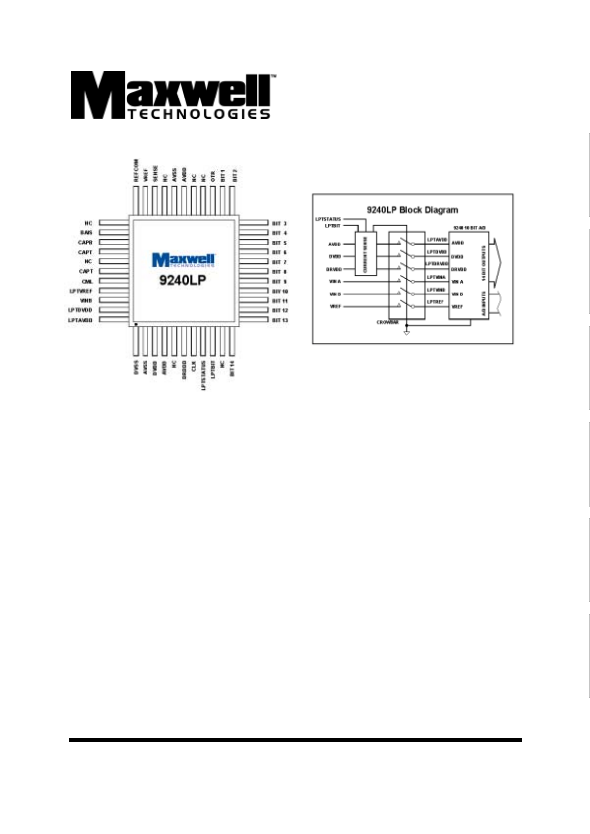
TABLE 1. 9240LP PIN DESCRIPTION
PIN NUMBER NAME DESCRIPTION
1 DVSS Digital Ground
2, 29 AVSS Analog Ground
3 DVDD 5V Digital Supply
4, 28 AVDD 5V Analog Supply
5 NC No Connect
6 DRVDD Digital Output Driver Supply
7 CLK Clock Input Pin
8 LPTSTATUS A 0 to 5V pulse is output during the decision
time and protect time. Normally low.
9 LPTBIT The LPT circuit will crowbar the power supplies
to the 9240LP for as long as a logic high is
applied. Used to verify operation of the LPT.
Normally a logical low or ground is applied to
this input.
10 NC No Connect
11 BIT 14 Least Significant Data Bit (LSB)
12-23 BIT 13-BIT 2 Data Output Bits
24 BIT 1 Most Significant Data Bits (MSB)
25 OTR Out of Range
26, 27, 30 NC No Connect
31 SENSE Reference Select
32 V
REF
Reference I/O
33 REFCOM Reference Common
34, 38 NC No Connect
35 BIAS Power/Speed Programming
36 CAPB Noise Reduction Pin
37 CAPT Noise Reduction Pin
39 CML Common-Mod Level (Midsupply)
40 LPTV
REF
Protected Reference I/O
41 V
IN
A Analog Input Pin (+)
42 V
IN
B Analog Input Pin (-)
43 LPTDVDD Protected 5V Digital Supply
44 LPTAVDD Protected 5V Analog Supply
Memory
3
All data sheets are subject to change without notice
©2002 Maxwell Technologies
All rights reserved.
14-Bit, 10 MSPS Monolithic A/D Converter with LPT ASIC
9240LP
03.08.02 Rev 4
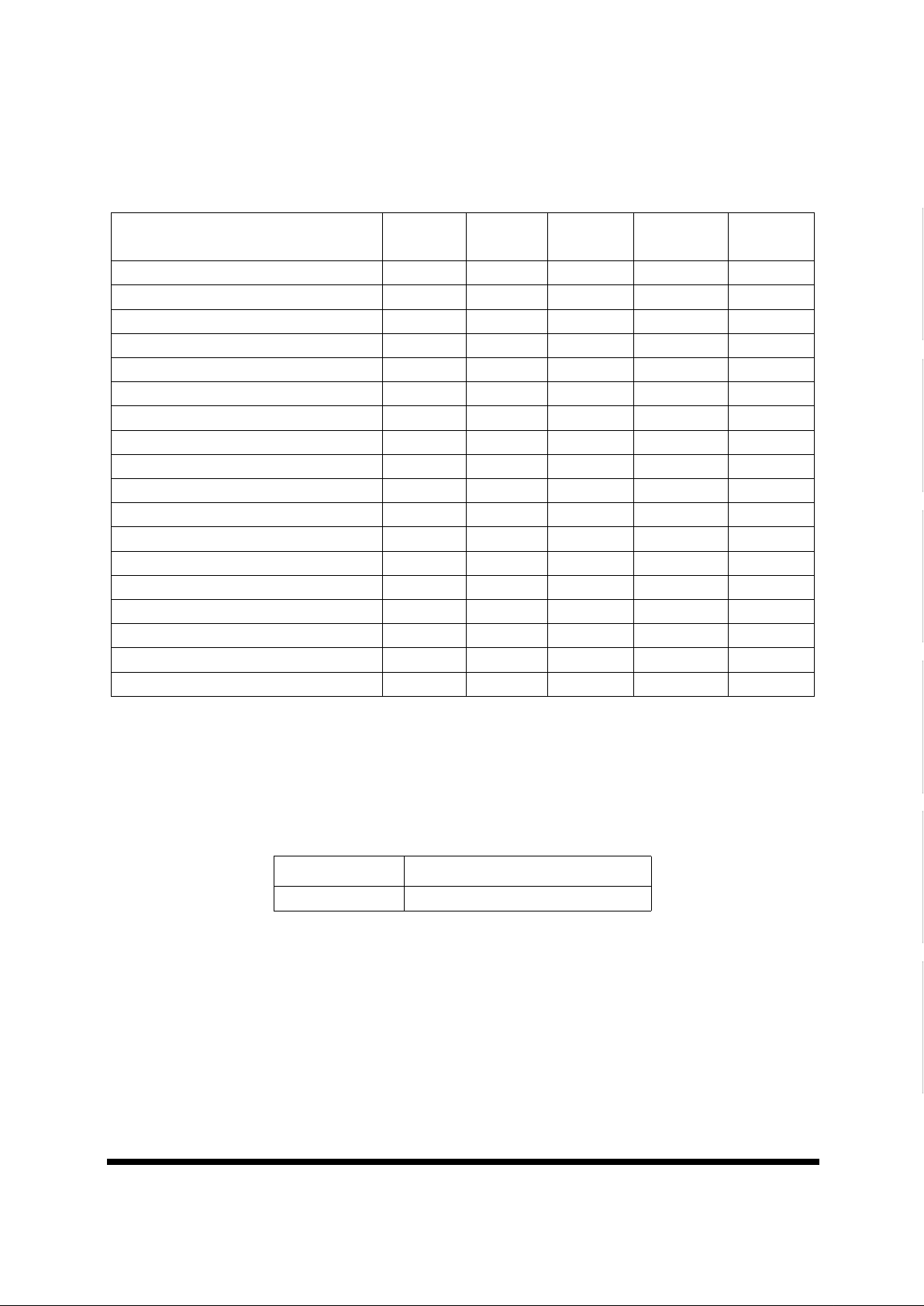
TABLE 2. 9240LP ABSOLUTE MAXIMUM RATINGS
1
1. Stresses above those listed under Absolute Maximum Ratings may cause permanent damage to the device. This is a stress
rating only; functional operation of the device at these or any other conditions above those indicated in the operational sections of this specification are not implied. Exposure to absolute maximum ratings for extended periods may effect device reliability.
P
ARAMETER SYMBOL
WITH RESPECT
T
O
MIN MAX UNIT
+5 V Analog Supply AVDD AVSS -0.3 6.5 V
+5 V Digital Supply DVDD DVSS -0.3 6.5 V
Analog Ground AVSS DVSS -0.3 0.3 V
+5 V Analog Supply AVDD DVDD -6.5 6.5 V
Digital Output Driver Supply DRVDD DRVSS -0.3 6.5 V
Digital Output Driver Ground DRVSS AVSS -0.3 0.3 V
Reference Common REFCOM AVSS -0.3 0.3 V
Clock Input Pin CLK AVSS -0.3 AVDD V
Digital Outputs Data Out Bits DRVSS -0.3 DVDD V
Analog Inputs V
IN
A, VINB AVSS -0.3 AVDD V
Reference I/O V
REF
AVSS -0.3 AVDD V
Reference Select Sense AVSS -0.3 AVDD V
Noise Reduction Pins CAPB, CAPT AVSS -0.3 AVDD V
Power/Speed Programming BIAS AVSS -0.3 AVDD - 0.6 V
Junction Temperature T
J
-- 150
°
C
Operating Temperature T
A
-55 125 °C
Storage Temperature T
STG
-65 150
°
C
Lead Temperature (10 sec) T
L
-- 300
°
C
TABLE 3. DELTA LIMITS
PARAMETER VARIATION
I
CC
±10% OF SPECIFIED VALUE IN TABLE 4
 Loading...