

MAXWELL 89C1632RPQK30, 89C1632RPQK25, 89C1632RPQK20, 89C1632RPQI30, 89C1632RPQI25 Datasheet
...
1
Memory
All data sheets are subject to change without notice
(619) 503-3300 - Fax: (619) 503-3301 - www.maxwell.com
16 Megabit (512K x 32-Bit)
89C1632
©2001 Maxwell Technologies.
All rights reserved.
MCM SRAM
12.20.01 Rev 1
1000558
FEATURES:
• Four 512k x 8 SRAM architecture
•R
AD-PAK® technology hardens against natural space radia-
tion technology
• Total dose hardness:
- > 100 krad (Si), depending upon space mission
• Excellent Single Event Effects:
- SEL > 68 MeV/mg/cm
2
- SEU threshold = 3 MeV/mg/cm
2
- SEU saturated cross section: 6E-9 cm2/bit
• Package: 68-pin quad flat package
• Fast access time: 20, 25 and 30 ns
• Completely static memory - no clock or timing strobe
required
• Internal bypass capacitor
• High-speed silicon-gate CMOS technology
• 5V or 3V ± 10% power supply
• Equal address and chip enable access times
• Three-state outputs
• All inputs and outputs are TTL compatible
DESCRIPTION:
Maxwell Technologies’ 89C1632 high-performance 16 Megabit Multi-Chip Module (MCM) Static Random Access Memory
features a greater than 100 krad (Si) total dose tolerance,
depending upon space mission. The four 4-Megabyte SRAM
die and bypass capacitors are incorporated into a high-reliable
hermetic quad flat-pack ceramic package. With high-performance silicon-gate CMOS technology, the 89C1632 reduces
power consumption and eliminates the need for external
clocks or timing strobes. It is equipped with output enable
(OE
) and four byte enable (CS1 - CS4) inputs to allow greater
system flexibility. When OE
input is high, the output is forced
to high impedance.
Maxwell Technologies' patented R
AD-PAK® packaging technol-
ogy incorporates radiation shielding in the microcircuit package. In a GEO orbit, R
AD-PAK provides true greater than 100
krad (Si) total radiation dose tolerance, dependent upon space
mission. It eliminates the need for box shielding while providing the required radiation shielding for a lifetime in orbit or a
space mission. This product is available in Class H or Class K
packaging and screening.
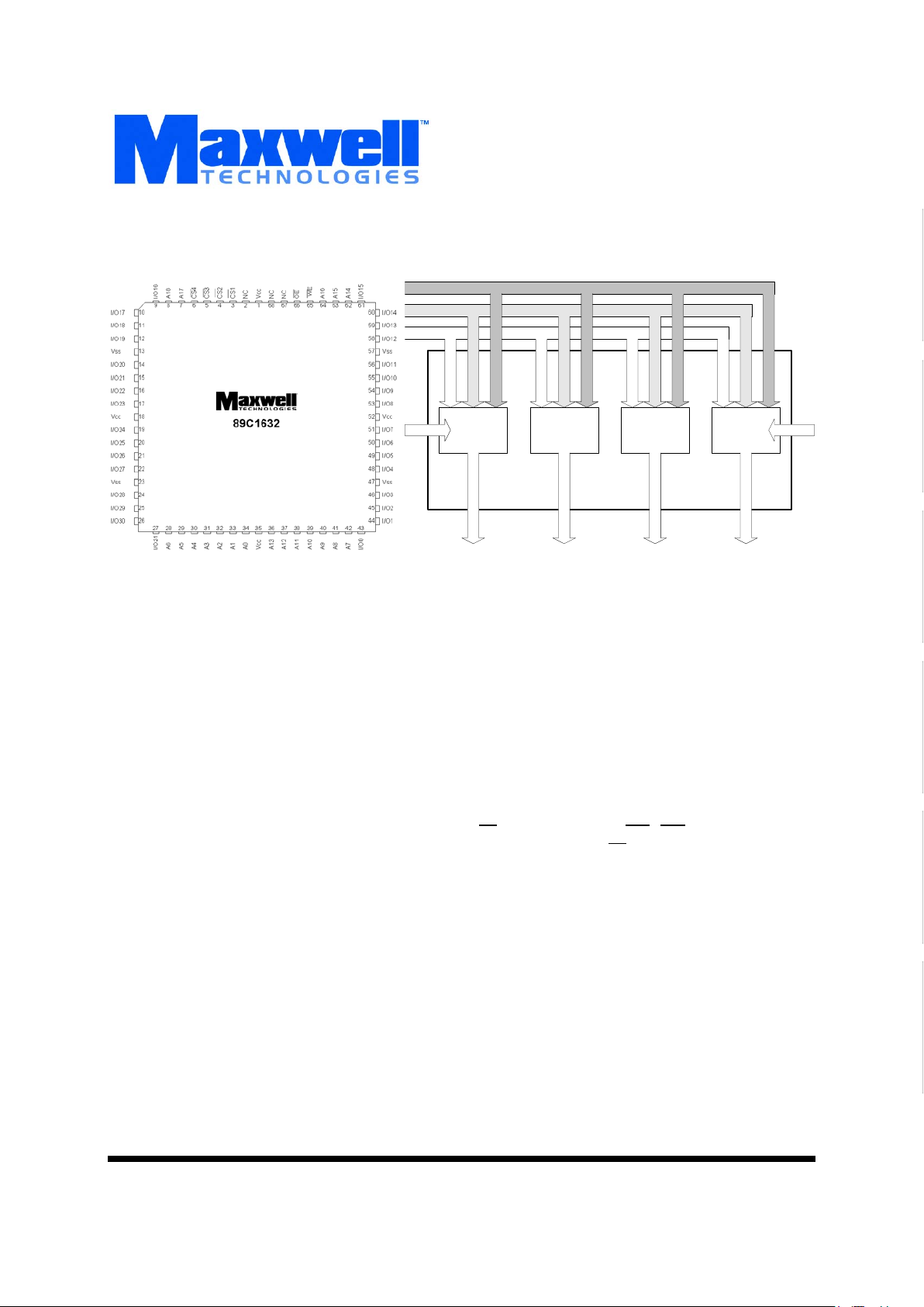
CS 1-4
MCM
OE, WE
Address
4Mb SRAM 4Mb SRAM 4Mb SRAM 4Mb SRAM
Power Ground
I/O 0-7 I/O 8-15 I/O 16-23 I/O 24-31
16 Megabit (512k x 32-bit) SRAM MCM
Logic Diagram
Memory
2
All data sheets are subject to change without notice
©2001 Maxwell Technologies.
All rights reserved.
16 Megabit (512K x 32-Bit) MCM SRAM
89C1632
12.20.01 Rev 1
1000558
TABLE 1. PINOUT DESCRIPTION
PIN SYMBOL DESCRIPTION
34-28, 42-36, 62-64, 7, 8 A0-A18 Address Enable
65 WE
WriteEnable
66 OE
Output Enable
3-6 CS1
- CS4 Chip Enable
43-46, 48-56, 58-61, 9-12,
14-17, 19-22, 24-27
I/O0-I/O31 Data Input/Output
2, 67, 68 NC No Connection
1, 18, 35, 52 V
CC
+5V Power Supply
13, 23, 47, 57 V
SS
Ground
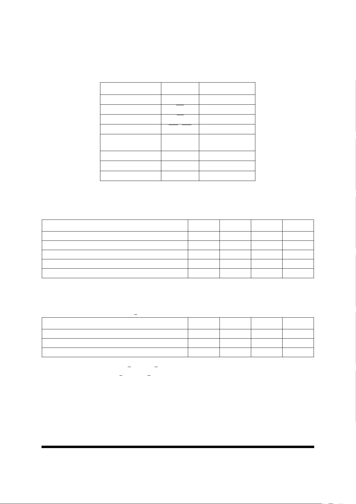
TABLE 2. 89C1632 ABSOLUTE MAXIMUM RATINGS
(VOLTAGE REFERENCED TO VSS = 0V)
P
ARAMETER SYMBOL MIN MAX UNITS
Power Supply Voltage Relative to V
SS
V
CC
-0.5 +7.0 V
Voltage Relative to V
SS
for Any Pin Except V
CC
VIN, V
OUT
-0.5 VCC+0.5 V
Power Dissipation P
D
-- 4.0 W
Operating Temperature T
A
-55 +125
°
C
Storage Temperature T
S
-65 +150
°
C
TABLE 3. 89C1632 RECOMMENDED OPERATING CONDITIONS
(VCC = 5.0 + 10%, TA = -55 TO +125 °C, UNLESS OTHERWISE NOTED)
P
ARAMETER SYMBOL MIN MAX UNITS
Supply Voltage, (Operating Voltage Range) V
CC
4.5 5.5 V
Input High Voltage V
IH
2.2 VCC + 0.5
(1)
1. VIH (max) = VCC + 2V ac (pulse width < 10ns) for I < 80 mA.
V
Input Low Voltage V
IL
-0.5
(2)
2. VIL (min) = -2.0V ac; (pulse width < 20 ns) for I < 80 mA.
0.8 V
Memory
3
All data sheets are subject to change without notice
©2001 Maxwell Technologies.
All rights reserved.
16 Megabit (512K x 32-Bit) MCM SRAM
89C1632
12.20.01 Rev 1
1000558
TABLE 4. 89C1632 CAPACITANCE
(f = 1.0 MHZ, dV = 3.0V, TA = 25 °C)
P
ARAMETER SYMBOL TEST CONDITIONS MAX UNITS
Input Capacitance
1
CS1 - CS4,
OE
, WE
I/O0-7, I/O8-15, I/O16-23, I/O24-31
1. Guaranteed by design.
C
IN
V
IN
= 0 V
7
28
7
pF
Input / Output Capacitance
1
C
OUT
V
I/O
= 0 V 8 pF
TABLE 5. 89C1632 DC ELECTRICAL CHARACTERISTICS
(VCC = 5.0 + 10%, TA = -55 TO +125 °C, UNLESS OTHERWISE NOTED)
P
ARAMETER SYMBOL TEST CONDITIONS MIN TYP MAX UNITS
Input Leakage Current I
LI
VIN = 0 to V
CC
-8.0 -- +8.0 uA
Output Leakage Current I
LO
CS = VIH, V
OUT
= VSS to V
CC
-8.0 -- +8.0 uA
Average Operating Current
Cycle Time:
20 ns
25 ns
30 ns
I
CC
Min. Cycle, 100% Duty, CS = VIL, I
OUT
= 0 mA
V
IN
= VIH or V
IL
--
--
--
--
800
760
720
mA
Standby Power Supply Current I
SB
CS= VIH, cycle time > 25ns -- -- 240 mA
CMOS Standby Power Supply
Current
I
SB1
CS > VCC - 0.2V, f = 0 MHz, VIN > VCC
- 0.2V or
V
IN <
0.2V
-- -- 60 mA
Output Low Voltage V
OLIOL
= + 8.0 mA -- -- 0.4 V
Output High Voltage V
OHIOH
= -4.0 mA 2.4 -- -- V
TABLE 6. 89C1632 AC OPERATING CONDITIONS AND CHARACTERISTICS
(VCC = 5.0 + 10%, TA = -55 TO +125 °C, UNLESS OTHERWISE NOTED)
P
ARAMETER MIN TYP MAX UNITS
Input Pulse Level 0.0 -- 3.0 V
Output Timing Measurement Reference Level -- -- 1.5 V
Input Rise/Fall Time -- -- 3.0 ns
Input Timing Measurement Reference Level -- -- 1.5 V
Memory
4
All data sheets are subject to change without notice
©2001 Maxwell Technologies.
All rights reserved.
16 Megabit (512K x 32-Bit) MCM SRAM
89C1632
12.20.01 Rev 1
1000558
TABLE 7. 89C1632 READ CYCLE
(VCC = 5.0 + 10%, TA = -55 TO +125 °C, UNLESS OTHERWISE NOTED)
P
ARAMETER SYMBOL MIN TYP MAX UNITS
Read Cycle Time
-20
-25
-30
t
RC
20
25
30
--
--
--
--
--
--
ns
Address Access Time
-20
-25
-30
t
AA
--
--
--
--
--
--
20
25
30
ns
Chip Select to Output
-20
-25
-30
t
CO
--
--
--
--
--
--
20
25
30
ns
Output Enable to Output
-20
-25
-30
t
OE
--
--
--
--
--
--
10
12
14
ns
Output Enable to Low-Z Output
-20
-25
-30
t
OLZ
--
--
--
0
0
0
--
--
--
ns
Chip Enable to Low-Z Output
-20
-25
-30
t
LZ
--
--
--
3
3
3
--
--
--
ns
Output Disable to High-Z Output
-20
-25
-30
t
OHZ
--
--
--
5
6
8
--
--
--
ns
Chip Disable to High-Z Output
-20
-25
-30
t
HZ
--
--
--
5
6
8
--
--
--
ns
Output Hold from Address Change
-20
-25
-30
t
OH
3
3
3
--
--
--
--
--
--
ns
TABLE 8. 89C1632 FUNCTIONAL DESCRIPTION
CS WE OE MODE I/O PIN SUPPLY CURRENT
HX1X
1
Not Select High-Z ISB, I
SB1
 Loading...