


MAXWELL 8143RPFS, 8143RPFE, 8143RPFB Datasheet
PRELIMINARY
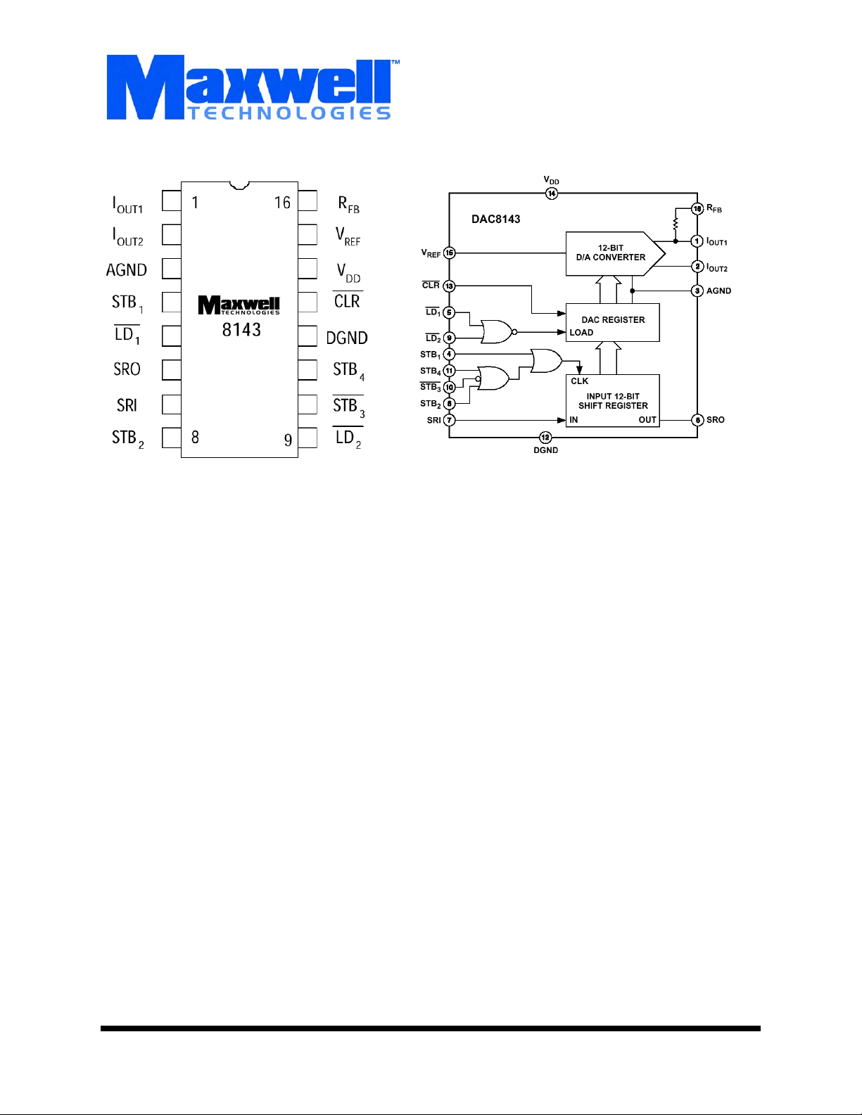
8143
12-Bit Serial Daisy Chain D/A
Converter
Memory
Logic Diagram
FEATURES:
• Microprocessor interfacing in serially controlled systems
• Buffered digital output pin for daisy-chaining multiple DACs
• Minimizes address-decoding in multiple DAC systems three wire interface for any number of DACs
- One data line
- One CLK line
- One load line
• Fast interface timing reduces timing design considerations
while minimizing microprocessor wait states.
• Improved resistance to ESD
•R
AD-PAK® radiation-hardened against natural space
radiation
• Total dose hardness:
- > 50 Krad (Si), depending upon space mission
• Package:
- 16 pin R
• Operating temperature: -40 to 85°C
AD-PAK® flat pack
DESCRIPTION:
Maxwell Technologies’ 8143 is a 12-bit serial-input daisy-chain
CMOS digital-to-analog converter (DAC) that features serial
data input and buffered serial data output and a greater than
50 krad (Si) total dose tolerance, dependent upon space mission. It was designed for multiple serial DAC systems, where
serially daisy-chaining one DAC after another is greatly simplified. The 8143 also minimizes address decoding lines
enabling simpler logic interfacing. It allows three-wire interface
for any number of DACs: one data line, one CLK line and one
load line. Serial data in the input register (MSB first) is
sequentially clocked out to the SRO pin as the new data word
(MSB first) is simultaneously clocked in from the SRI pin. The
strobe inputs are used to clock in/out data on the rising or falling (user selected) strobe edges (STB
When the shift register’s data has been updated, the new data
word is transferred to the DAC register with use of LO1 and
LD2 inputs.
Maxwell Technologies' patented R
ogy incorporates radiation shielding in the microcircuit package. It eliminates the need for box shielding while providing
the required radiation shielding for a lifetime in orbit or space
mission. In a GEO orbit, R
krad (Si) radiation dose tolerance. This product is available
with screening up to Class S.
AD-PAK provides greater than 50
, STB2, STB3, STB4).
1
AD-PAK® packaging technol-
1000599
(858) 503-3300- Fax: (858) 503-3301- www.maxwell.com
12.19.01 Rev 1
All data sheets are subject to change without notice
©2001 Maxwell Technologies
All rights reserved.
1
12-Bit Serial Daisy-Chain D/A Converter
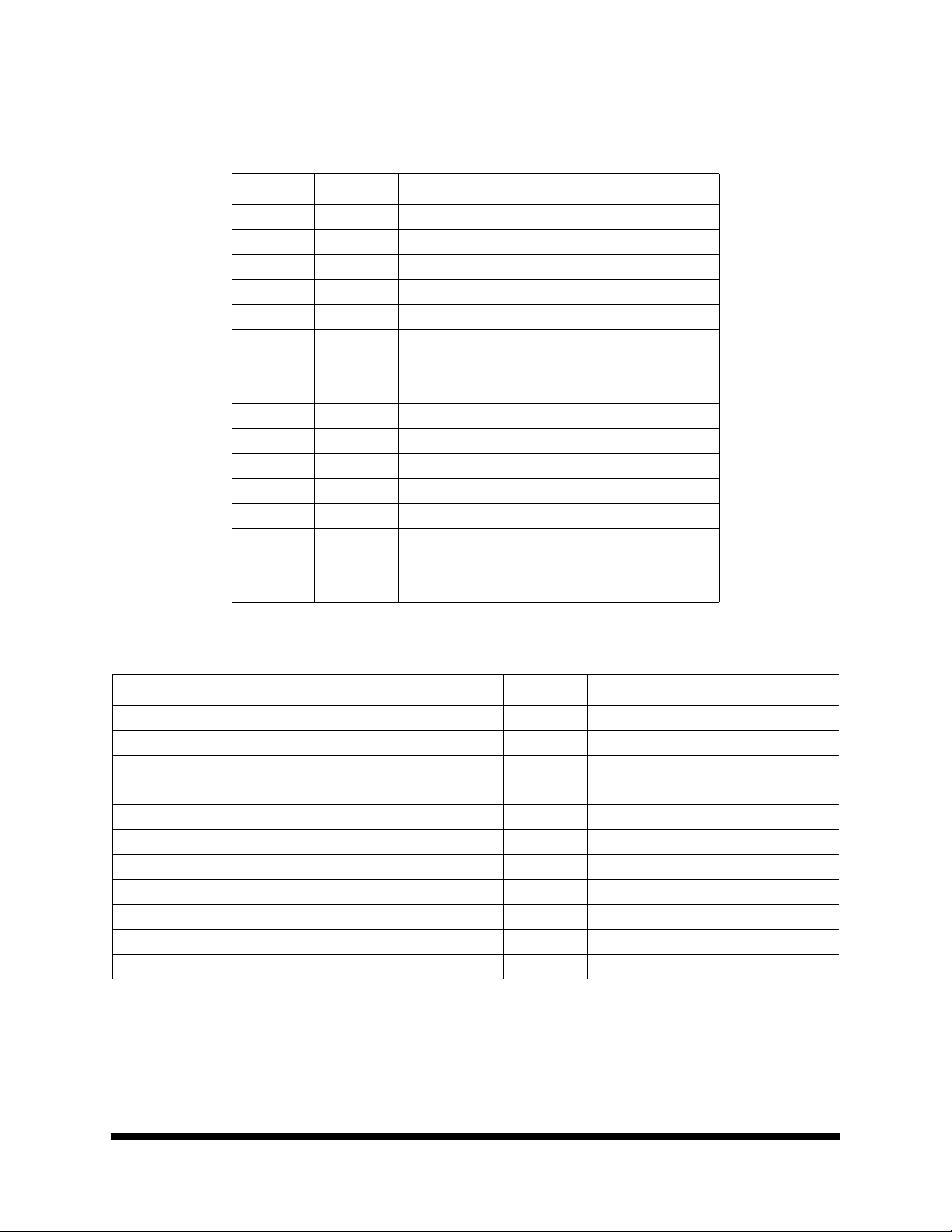
TABLE 1. 8143 PINOUT DESCRIPTION
PRELIMINARY
PIN SYMBOL DESCRIPTION
8143
1I
2I
OUT1
OUT2
Analog Out 1
Analog Out 2
3 AGND Analog Ground
4STB
5LD
Strobe 1
1
DAC Register Load 1
1
6 SRO Serial Data Out
7 SRI Serial Data In
8 STB2 Strobe 2
9R
10 V
11 V
FB
REF
DD
Feedback
Vlotage Reference
Positive Supply
12 CLR DAC Register Clear
13 DGND Digital Ground
14 STB
15 STB
16 LD
Strobe 4
4
Strobe 3
3
DAC Register Load 2
2
TABLE 2. 8143 ABSOLUTE MAXIMUM RATINGS
Memory
PARAMETER SYMBOL MIN MAX UNIT
VDD to DGND -- 17 V
V
to DGND -25 25 V
REF
V
to DGND -25 25 V
RFB
AGND to DGND -- V
DGND to AGND -- V
Digital Input Voltage Range -0.3 V
Output Voltage (Pin 1, Pin 2) -0.3 V
Operating Temperature Range T
Thermal Impedance
Storage Temperature T
Lead Temperature (Soldering, 60 sec) T
1000599
12.19.01 Rev 1
A
Θ
JC
STG
L
All data sheets are subject to change without notice
-40 85
-- 14.13
-65 150
-- 300
+ 0.3 V
DD
+ 0.3 V
CC
DD
DD
°
C/W
V
V
°
C
°
C
°
C
2
©2001 Maxwell Technologies.
All rights reserved.

12-Bit Serial Daisy-Chain D/A Converter
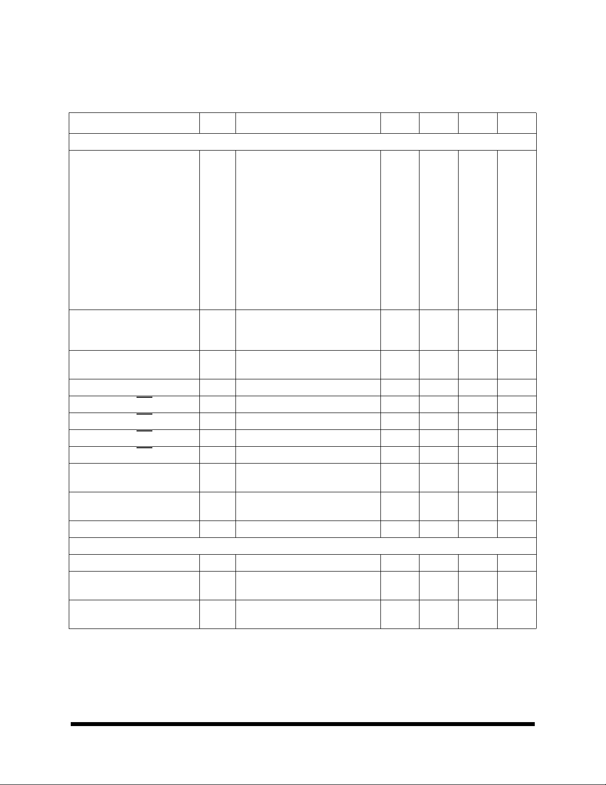
TABLE 3. 8143 ELECTRICAL CHARACTERISTICS
(@ VDD = 5V, V
PRELIMINARY
P
ARAMETER SYMBOL CONDITIONS MIN TYP MAX UNIT
STATIC ACCURACY
Resolution N 12 -- -- Bits
Nonlinearity INL -- -- ±1 LSB
Differential Nonlinearity
Gain Error
2
Gain Tempco (DGain/DTemp)
Power Supply Rejection Ratio
(DGain/DVDD)
Output Leakage Current
Zero Scale Error
Input Resistance
AC PERFORMANCE
Output Current Settling Time
AC Feed through Error (V
3,9
I
)
OUT1
Digital-to-Analog Glitch Energy
Total Harmonic Distortion
Output Noise Voltage Density
DIGITAL INPUTS/OUTPUTS
Digital Input HIGH V
Digital Input LOW V
Input Leakage Current
Input Capacitance C
Digital Output High V
Digital Output Low V
ANALOG OUTPUTS
Output Capacitance
Output Capacitance
= 10V; V
REF
5,6
7
3
3
= V
OUT1
1
3
= V
OUT2
DNL -- -- ±1 LSB
G
FSE
TC
GFS
PSRR DV
4
REF
3,8
to
3,10
I
LKGTA
I
ZSETA
R
IN
t
S
FT V
QV
= V
AGND
R
ATINGS, UNLESS OTHERWISE SPECIFIED)
= 0V; TA = FULL TEMPERATURE RANGE SPECIFIED UNDER ABSOLUTE MAXIMUM
DGND
-- -- ±2 LSB
-- -- ±5 ppm/°C
= ±5% -- ±0.0006 ±0.002 %/%
DD
= 25°C
T
= Full Temperature Range
A
= 25°C
T
= Full Temperature Range
A
V
Pin 7 11 15 kΩ
REF
--
--
--
--
--
--
±0.002
±0.01
±5
±25
±0.03
±0.15
-- 0.380 1 µs
= 20V p-p @ f = 10 KHz, TA =
REF
°
25
C
REF
= 0V, I
load = 100 Ω, C
OUT
EXT
=
-- -- 2.0 mV p-p
-- -- 20 nVs
13 pF
3
3,11
12
THD V
= 6V rms @ 1 KHz
REF
DAC register loaded with all 1s
en10 Hz to 100 KHz between RFB and
I
OUT
IH
IL
I
VIN = 0V to 5V -- -- ±1 µA
IN
VIN = 0V -- -- 8 pF
IN
OHIOH
OLIOL
C
OUT1
C
OUT2
C
OUT1
C
OUT2
= -200 µA 4 -- -- V
= 1.6 mA -- -- 0.4 V
Digital Inputs = All 1s
Digital Inputs = All 0s
Digital Inputs = All 0s
Digital Inputs = All 1s
--
--
--
--
--
-92
-- -- 13 nV/√Hz
2.4 -- -- V
-- -- 0.8 V
--
--
--
--
--
--
--
--
90
90
60
60
8143
nA
Memory
LSB
dB
pF
pF
1000599
12.19.01 Rev 1
All data sheets are subject to change without notice
©2001 Maxwell Technologies.
All rights reserved.
3
12-Bit Serial Daisy-Chain D/A Converter
TABLE 3. 8143 ELECTRICAL CHARACTERISTICS
(@ VDD = 5V, V
PRELIMINARY
P
ARAMETER SYMBOL CONDITIONS MIN TYP MAX UNIT
TIMING CHARACTERISTICS
Serial Input to Strobe Setup Times
(t
= 80 ns) t
STB
= 10V; V
REF
OUT1
3
= V
OUT2
t
t
t
t
t
= V
DS1
DS2
DS3
DS4
DH1
DH2
= V
AGND
DGND
R
ATINGS, UNLESS OTHERWISE SPECIFIED)
STB1 used as the strobe
STB
used as the strobe
2
STB
used as the strobe TA = 25 °C
3
T
= full temperature range
A
STB
used as the strobe
4
STB
used as the strobe TA = 25 °C
1
T
= full temperature range
A
STB
used as the strobe TA = 25 °C
2
T
= full temperature range
A
= 0V; TA = FULL TEMPERATURE RANGE SPECIFIED UNDER ABSOLUTE MAXIMUM
50
20
10
20
20
40
50
50
--
--
--
--
--
--
--
--
8143
ns
--
--
--
--
--
--
--
--
Serial Input to Strobe Hold Times
(t
= 80 ns) t
STB
STB to SRO Propagation Delay
13
SRI Data Pulsewidth t
STB
Pulsewidth (STB1 = 80 ns)
1
STB
Pulsewidth (STB2 = 100 ns) t
2
STB
Pulsewidth (STB3 = 80 ns) t
3
STB
Pulsewidth (STB4 = 80 ns) t
4
Load Pulsewidth t
14
t
LD1
LSB Strobe into Input Register to
Load DAC Register Time
CLR Pulsewidth t
POWER SUPPLY CHARACTERISTICS
Supply Voltage V
Supply Current I
Power Dissipation P
STB3 used as the strobe
DH3
STB
t
DH4
t
PD
SRI
STB1
STB2
STB3
STB4
, t
t
ASB
CLR
DD
DD
LD2TA
used as the strobe
4
TA = 25 °C
T
= full temperature range
A
= 25 °C
T
= temperature range
A
All digital inputs = VIH or V
All digital inputs = 0V or V
Digital inputs = 0V or VDD, 5V x 0.1 mA
D
Digital inputs = V
or VIL, 5V x 2 mA
IH
DD
60
--
--
Memory
ns
80
80
--
--
--
--
--
--
--
--
220
300
ns
100 -- -- ns
80 -- -- ns
80 -- -- ns
80 -- -- ns
80 -- -- ns
140
180
--
--
--
ns
--
0----ns
80 -- -- ns
4.75 5 5.25 V
IL
--
--
--
--
--
--
--
--
2
0.1
0.5
10
mA
mW
1. All grades are monotonic to 12 bits over temperature.
2. Using internal feedback resistor.
3. Guaranteed by design and not tested.
4. Applies to I
5. V
= 10V, all digital inputs = 0V.
REF
1000599
; all digital inputs = VIL, V
OUT
= 10V; specification also applied for I
REF
12.19.01 Rev 1
when all digital inputs = VIH.
OUT2
All data sheets are subject to change without notice
©2001 Maxwell Technologies.
All rights reserved.
4
12-Bit Serial Daisy-Chain D/A Converter
8143
6. Calculated from worst case R
7. Absolute temperature coefficient is less than 300 ppm/
8. I
, Load = 100 Ω. C
OUT
9t, where t equals measured time constant of the final RC decay.
PRELIMINARY
9. All digital inputs = 0V.
10.V
= 0V, all digital inputs = 0V to VDD or VDD to 0V.
REF
11.Calculations from e
K = Boltzmann constant, J/KR = resistance
T = resistor temperature, K R = bandwidth, Hz
12.Digital input are CMOS gates; I
13.Measured from active strobe edge (STB) to new data output at SRO; C
14.Minimum low time pulsewidth for STB
EXT
= ÷4K TRB where:
n
: I
(in LSBs) = (R
REF
ZSE
= 13 pF, digital input = 0V to VDD or VDD to 0V. Extrapolated to 1/2 LSB: ts = propagation delay (tPD) +
REF
x I
LKG
°
C.
Ω
typically 1 nA at 25 °C.
IN
, STB2, and STB4, and minimum high time pulsewidth for STB3.
1
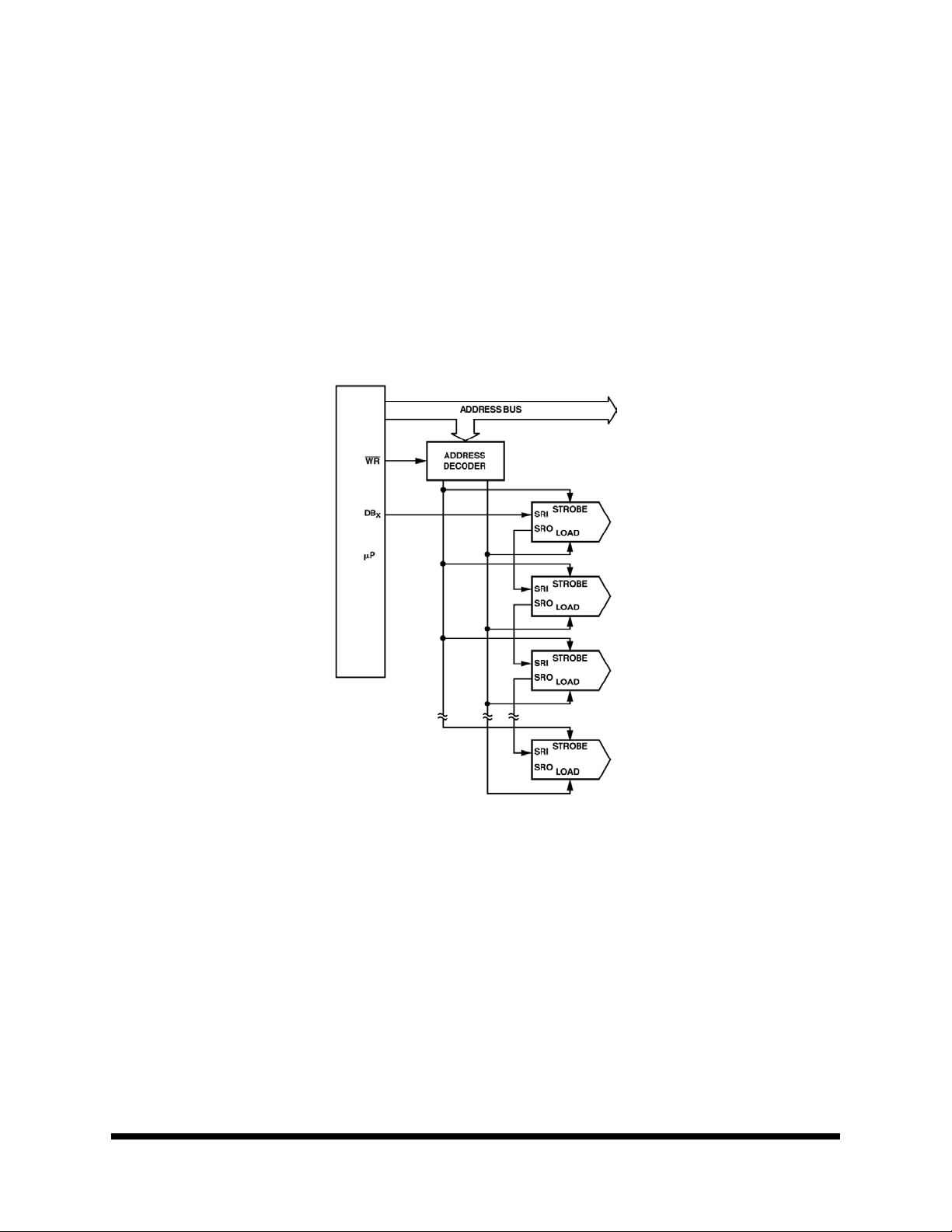
FIGURE 1. MULTIPLE WITH THREE-WIRE INTERFACE
x 4096)/V
.
REF
= 50 pF.
L
Memory
1000599
12.19.01 Rev 1
All data sheets are subject to change without notice
©2001 Maxwell Technologies.
All rights reserved.
5
12-Bit Serial Daisy-Chain D/A Converter
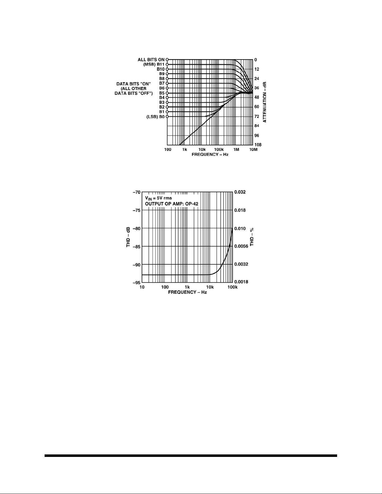
FIGURE 2. MULTIPLYING MODE FREQUENCY RESPONSE VS. DIGITAL CODE
PRELIMINARY
FIGURE 3. MULTIPLYING MODE TOTAL HARMONIC DISTORTION VS. FREQUENCY
8143
Memory
1000599
12.19.01 Rev 1
All data sheets are subject to change without notice
©2001 Maxwell Technologies.
All rights reserved.
6

12-Bit Serial Daisy-Chain D/A Converter
FIGURE 4. SUPPLY CURRENT VS. LOGIC INPUT VOLTAGE
PRELIMINARY
FIGURE 5. LINEARITY ERROR VS. DIGITAL CODE
8143
Memory
1000599
12.19.01 Rev 1
All data sheets are subject to change without notice
©2001 Maxwell Technologies.
All rights reserved.
7
12-Bit Serial Daisy-Chain D/A Converter
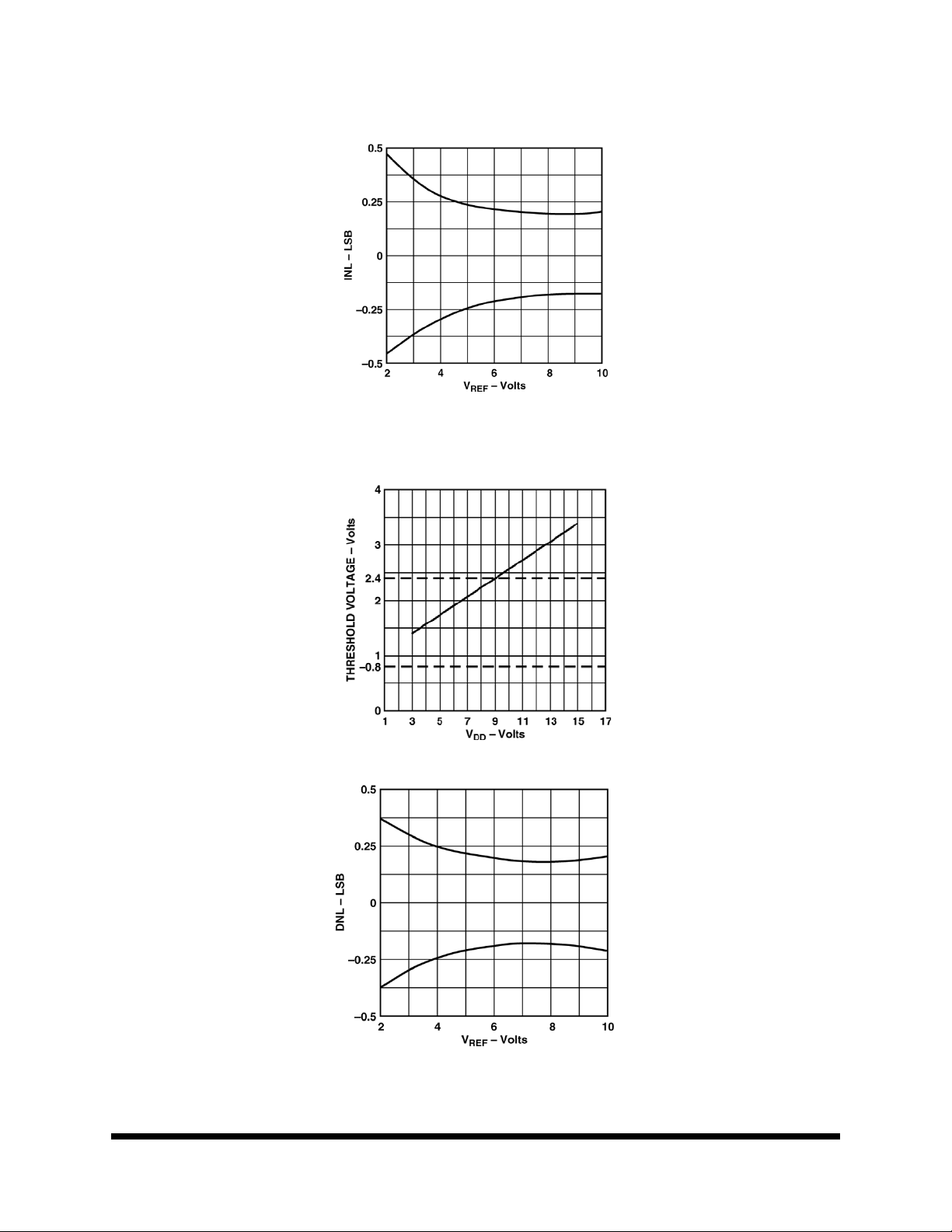
FIGURE 6. LINEARITY ERROR VS. REFERENCE VOLTAGE
PRELIMINARY
FIGURE 7. LOGIC THRESHOLD VOLTAGE VS. SUPPLY VOLTAGE
8143
Memory
1000599
FIGURE 8. DNL ERROR VS. REFERENCE VOLTAGE
12.19.01 Rev 1
All data sheets are subject to change without notice
8
©2001 Maxwell Technologies.
All rights reserved.