

MAXWELL 79C0408RT4FH12, 79C0408RT4FE20, 79C0408RT4FE15, 79C0408RT4FE12, 79C0408RT2FK20 Datasheet
...
1
Memory
All data sheets are subject to change without notice
(858) 503-3300 - Fax: (858) 503-3301- www.maxwell.com
4 Megabit (512k x 8-bit)
EEPROM MCM
79C0408
©2002 Maxwell Technologies
All rights reserved.
03.20.02 Rev 10
• Four 128k x 8-bit EEPROMs MCM
•R
AD-PAK® radiation-hardened against natural space radia-
tion
• Total dose hardness:
- > 100 krad (Si)
- Dependent upon orbit
• Excellent Single Event Effects
- SEL > 120 MeV/mg/cm
2
- SEU > 90 MeV/mg/cm2 read mode
- SEU = 18 MeV/mg/cm
2
write mode
• Package: 40 pin R
AD-PAK® flat pack
• High speed:
- 120, 150, and 200 ns maximum access times
available
•Data
Polling and Ready/Busy signal
• Software data protection
• Write protection by RES
pin
• High endurance
- 10,000 erase/write (in Page Mode), 10 year data reten-
tion
• Page write mode: 1 to 128 byte page
• Low power dissipation
- 88 mW/MHz active mode
- 440 µW standby mode
DESCRIPTION:
Maxwell Technologies’ 79C0408 multi-chip module (MCM)
memory features a greater than 100 krad (Si) total dose tolerance, dependent upon orbit. Using Maxwell Technologies’ patented radiation-hardened R
AD-PAK® MCM packaging
technology, the 79C0408 is the first radiation-hardened 4
Megabit MCM EEPROM for space applications. The 79C0408
uses four 1 Megabit high-speed CMOS die to yield a 4 Megabit product. The 79C0408 is capable of in-system electrical
Byte and Page programmability. It has a 128 bytes Page Programming function to make its erase and write operations
faster. It also features Data Polling and a Ready/Busy signal to
indicate the completion of erase and programming operations.
In the 79C0408, hardware data protection is provided with the
RES
pin, in addition to noise protection on the WE signal and
write inhibit on power on and off. Software data protection is
implemented using the JEDEC optional standard algorithm.
Maxwell Technologies' patented R
AD-PAK® packaging technol-
ogy incorporates radiation shielding in the microcircuit package. It eliminates the need for box shielding while providing
the required radiation shielding for a lifetime in orbit or space
mission. In a GEO orbit, R
AD-PAK provides greater than 100
krad (Si) radiation dose tolerance. This product is available
with screening up to Class K.
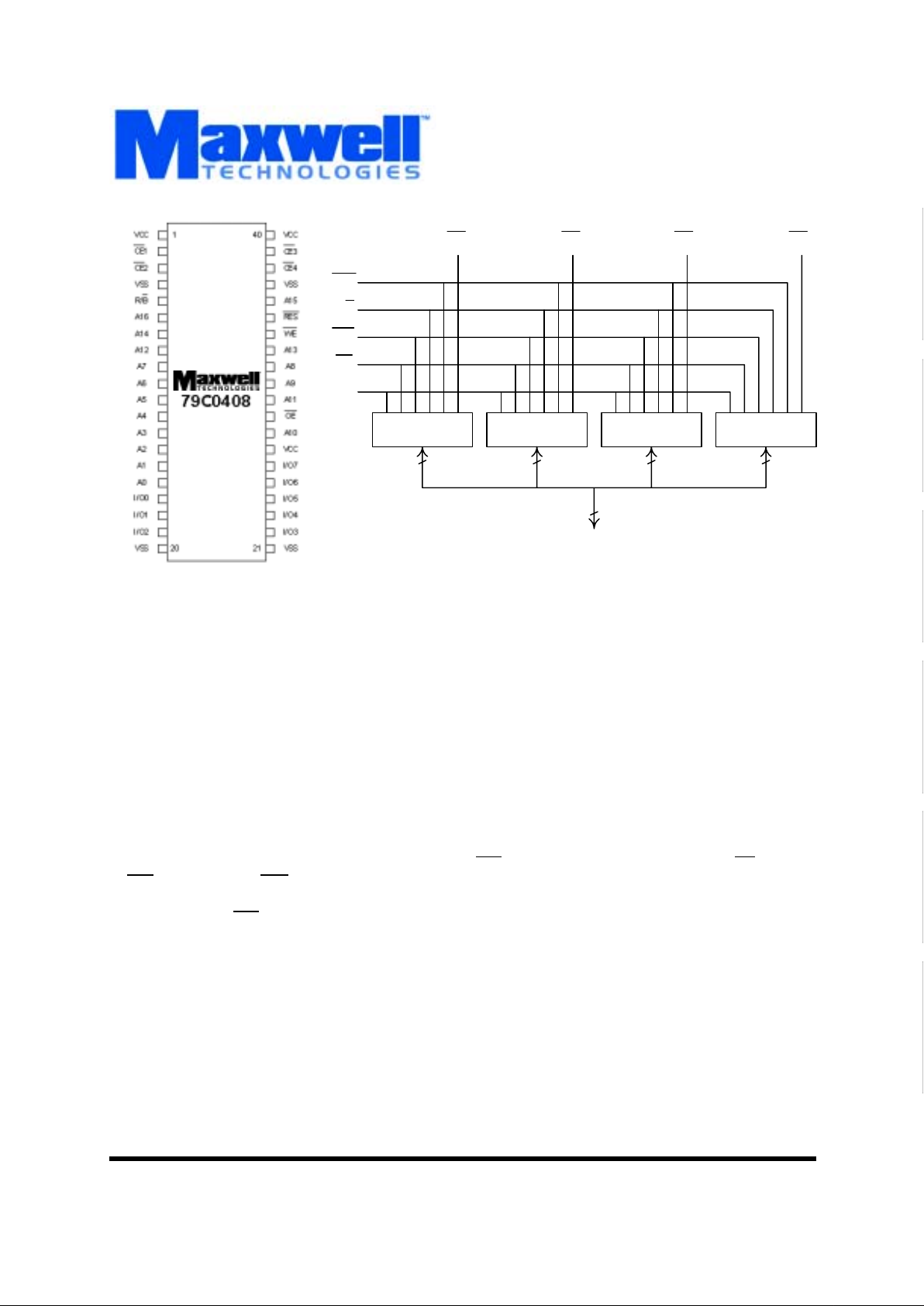
128K x 8 128K x 8 128K x 8 128K x 8
I/O
0-7
A
0-16
WE
R/ B
RES
OE
CE
1
CE
2
CE
3
CE
4
FEATURES:
Memory
2
All data sheets are subject to change without notice
©2002 Maxwell Technologies
All rights reserved.
4 Megabit (512k x 8-bit) EEPROM MCM
79C0408
03.20.02 Rev 10
1. VIN MIN = -3.0V FOR PULSE WIDTH <50NS.
TABLE 1. 79C0408 PIN DESCRIPTION
PIN SYMBOL DESCRIPTION
16-9, 32-31,
28, 30, 8, 33,
7, 36, 6
A0 to A16 Address Input
17-19, 22-26 I/O0 to I/O7 Data Input/Output
29 OE
Output Enable
2, 3, 38, 39 CE1-4
Chip Enable 1 through 4
34 WE
Write Enable
1, 27, 40 VCC Power Supply
4, 20, 21, 37 VSS Ground
4RDY/BUSY
Ready/Busy
35 RES
Reset
TABLE 2. 79C0408 ABSOLUTE MAXIMUM RATINGS
PARAMETER SYMBOL MIN MAX UNIT
Supply Voltage V
CC
-0.6 7.0 V
Input Voltage V
IN
-0.5
1
7.0 V
Operating Temperature Range T
OPR
-55 125
°
C
Storage Temperature Range T
STG
-65 150
°
C
TABLE 3. 79C0408 RECOMMENDED OPERATING CONDITIONS
PARAMETER SUBGROUPS SYMBOL MIN MAX UNIT
Supply Voltage 1 V
CC
4.5 5.5 V
Input Voltage
RES
_PIN
1V
IL
V
IH
V
H
-0.3
1
2.2
V
CC
-0.5
1. V
IL
min = -1.0V for pulse width < 50 ns
0.8
V
CC
+0.3
V
CC
+1
V
V
V
Case Operating Temperature 1 T
C
-55 125
°
C
Memory
3
All data sheets are subject to change without notice
©2002 Maxwell Technologies
All rights reserved.
4 Megabit (512k x 8-bit) EEPROM MCM
79C0408
03.20.02 Rev 10
TABLE 4. 79C0408 CAPACITANCE
1
(TA = 25 °C, f = 1 MHz)
1. Guaranteed by design.
P
ARAMETER SYMBOL MIN MAX UNIT
Input Capacitance: VIN = 0 V
2
WE
CE
1-4
OE
A
0-16
2. Guaranteed by design.
C
IN
--
--
--
--
24
6
24
24
pf
Output Capacitance: V
OUT
= 0 V
2
C
OUT
48 pF
TABLE 5. 79C0408 DC ELECTRICAL CHARACTERISTICS
(VCC = 5V ±10%, TA = -55 TO +125°C)
P
ARAMETER TEST CONDITION SUBGROUPS SYMBOL MIN MAX UNITS
Input Leakage Current VCC = 5.5V, VIN = 5.5V
1
1, 2, 3 I
IL
µA
CE
1-4
1, 2, 3 -- 2
1
1. ILI on RES = 100 uA max.
OE
, WE
1-4
1, 2, 3 -- 4
A
0-16
1, 2, 3 -- 4
Output Leakage Current V
CC
= 5.5V, V
OUT
= 5.5V/0.4V 1, 2, 3 I
LO
-- 2 µA
Standby V
CC
Current
2
2. One CE
active.
CE
= V
CC
1, 2, 3 I
CC1
-- 20 µA
CE
= V
IH
1, 2, 3 I
CC2
-- 1 mA
Operating V
CC
Current I
OUT
= 0mA, Duty = 100%, Cycle = 1µs at
V
CC
= 5.5V
1, 2, 3 I
CC3
-- 15 mA
I
OUT
= 0mA, Duty = 100%, Cycle = 150ns
at V
CC
= 5.5V
1, 2, 3 -- 50
Input Voltage
RES
_PIN
1, 2, 3 V
IL
-- 0.8 V
1, 2, 3 V
IH
2.2 --
1, 2, 3 V
H
VCC -0.5 --
Output Voltage I
OL
= 2.1 mA 1, 2, 3 V
OL
-- 0.4 V
I
OH
= -0.4 mA 1, 2, 3 V
OH
2.4 --
Memory
4
All data sheets are subject to change without notice
©2002 Maxwell Technologies
All rights reserved.
4 Megabit (512k x 8-bit) EEPROM MCM
79C0408
03.20.02 Rev 10
TABLE 6. 79C0408 AC ELECTRICAL CHARACTERISTICS FOR READ OPERATIONS
1
(VCC = 5V ±10%, TA = -55 TO +125°C)
1. Test conditions: Input pulse levels - 0.4V to 2.4V; input rise and fall times < 20ns; output load - 1 TTL gate + 100pF (including scope
and jig); reference levels for measuring timing - 0.8V/1.8V.
P
ARAMETER SUBGROUPS SYMBOL MIN MAX UNIT
Address Access Time CE = OE = VIL, WE = V
IH
-120
-150
-200
9, 10, 11 t
ACC
--
--
--
120
150
200
ns
Chip Enable Access Time OE
= VIL, WE = V
IH
-120
-150
-200
9, 10, 11 t
CE
--
--
--
120
150
200
ns
Output Enable Access Time CE
= VIL, WE = V
IH
-120
-150
-200
9, 10, 11 t
OE
0
0
0
75
75
125
ns
Output Hold to Address Change CE
= OE = VIL, WE = V
IH
-120
-150
-200
9, 10, 11 t
OH
0
0
0
--
--
--
ns
Output Disable to High-Z
2
CE = VIL, WE = V
IH
-120
-150
-200
2. t
DF
and t
DFR
are defined as the time at which the output becomes an open circuit and data is no longer driven.
9, 10, 11 t
DF
0
0
0
50
50
60
ns
CE
= OE = VIL, WE = V
IH
-120
-150
-200
9, 10, 11 t
DFR
0
0
0
300
350
450
RES
to Output Delay CE = OE = VIL, WE = VIH
3
-120
-150
-200
3. Guaranteed by design.
t
RR
--
--
--
400
450
650
ns

Memory
5
All data sheets are subject to change without notice
©2002 Maxwell Technologies
All rights reserved.
4 Megabit (512k x 8-bit) EEPROM MCM
79C0408
03.20.02 Rev 10
TABLE 7. 79C0408 AC ELECTRICAL CHARACTERISTICS FOR WRITE OPERATIONS
(VCC = 5V ±10%, TA = -55 TO +125°C)
P
ARAMETER SUBGROUPS SYMBOL
MIN
1
MAX UNIT
Address Setup Time
-120
-150
-200
9, 10, 11 t
AS
0
0
0
--
--
--
ns
Chip Enable to Write Setup Time (WE
Controlled)
-120
-150
-200
9, 10, 11 t
CS
0
0
0
--
--
--
ns
Write Pulse Width
CE
Controlled
-120
-150
-200
WE
Controlled
-120
-150
-200
9, 10, 11
t
CW
t
WP
200
250
350
200
250
350
--
--
--
--
--
--
ns
Address Hold Time
-120
-150
-200
9, 10, 11 t
AH
150
150
200
--
--
--
ns
Data Setup Time
-120
-150
-200
9, 10, 11 t
DS
75
100
150
--
--
--
ns
Data Hold Time
-120
-150
-200
9, 10, 11 t
DH
10
10
20
--
--
--
ns
Chip Enable Hold Time (WE Controlled)
-120
-150
-200
9, 10, 11 t
CH
0
0
0
--
--
--
ns
Write Enable to Write Setup Time (CE
Controlled)
-120
-150
-200
9, 10, 11 t
WS
0
0
0
--
--
--
Write Enable Hold Time (CE
Controlled)
-120
-150
-200
9, 10, 11 t
WH
0
0
0
--
--
--

Memory
6
All data sheets are subject to change without notice
©2002 Maxwell Technologies
All rights reserved.
4 Megabit (512k x 8-bit) EEPROM MCM
79C0408
03.20.02 Rev 10
Output Enable to Write Setup Time
-120
-150
-200
9, 10, 11 t
OES
0
0
0
--
--
--
ns
Output Enable Hold Time
-120
-150
-200
9, 10, 11 t
OEH
0
0
0
--
--
--
ns
Write Cycle Time
2
-120
-150
-200
9, 10, 11 t
WC
--
--
--
10
10
20
ms
Data Latch Time
-120
-150
-200
9, 10, 11 t
DL
250
300
400
--
--
--
ns
Byte Load Window
-120
-150
-200
9, 10, 11 t
BL
100
100
200
--
--
--
µs
Byte Load Cycle
-120
-150
-200
9, 10, 11 t
BLC
0.55
0.55
0.95
30
30
30
µs
Time to Device Busy
-120
-150
-200
9, 10, 11 t
DB
100
120
170
--
--
--
ns
Write Start Time
3
-120
-150
-200
9, 10, 11 t
DW
150
150
250
--
--
--
ns
RES
to Write Setup Time
-120
-150
-200
9, 10, 11 t
RP
100
100
200
--
--
--
µs
V
CC
to RES Setup Time
4
-120
-150
-200
9, 10, 11 t
RES
1
1
3
--
--
--
µs
1. Use this divice in a longer cycle than this value.
2. t
WC
must be longer than this value unless polling techniques or RDY/BUSY are used. This device automatically completes the internal
write operation within this value.
TABLE 7. 79C0408 AC ELECTRICAL CHARACTERISTICS FOR WRITE OPERATIONS
(VCC = 5V ±10%, TA = -55 TO +125°C)
P
ARAMETER SUBGROUPS SYMBOL
MIN
1
MAX UNIT
 Loading...