

MAXWELL 7872RPFS, 7872RPFI, 7872RPFE, 7872RPFB, 7872RPDS Datasheet
...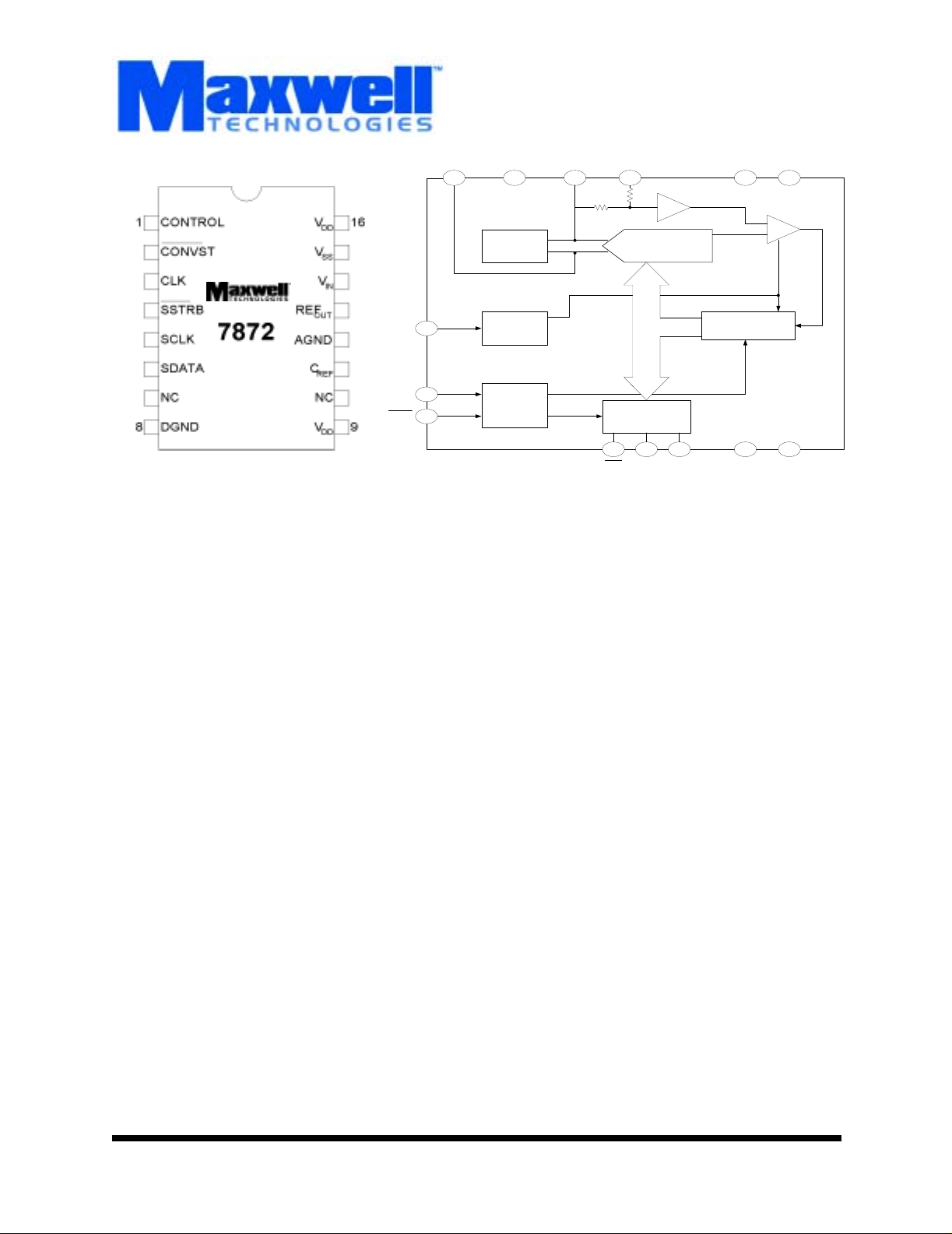
7872
14-Bit A/D Converter
FEATURES:
• 14-bit resolution and accuracy
• Total dose hardness:
- > 100 krad (Si), depending upon space mission
• Single event effects:
- SEL > 104 MeV/mg/cm
- SEUTH = 1.4 MeV/mg/cm
- SEU
= 1E-3 cm2/Device
Sat
• Package:
- 16 pin R
- 16 pin R
AD-PAK® flat package
AD-PAK® dual-in-line package
• Fast Conversion Times: 10 µs
• Low 50 mW typical power consumption
• High speed LC
2
MOS technology
- Analog input range of ±3V
- 83 KSPS throughput rate
- Operates with +5V/-5V power supplies
- 80 dB SNR at 10 kHz input frequency
- 2 s complement coding
- Serial output
2
2
CLK
CONTROL
CONVST
AGND C
12 11 13 14 9 16
3
1
2
REF
3V
REFERENCE
CLOCK
CONTROL
LOGIC
REF OUT V
IN
R
R
14-BIT DAC
SERIAL
INTERFACE
4 5 6
SSTRB SCLK SDATA DGND V
TRACK/HOLD
SAR + COUNTER
Logic Diagram
DESCRIPTION:
Maxwell Technologies’ 7872 high-speed 14-bit ADC microcircuit features a greater than 100 krad (Si) total dose tolerance;
depending upon orbit. The 7872 consists of a track/hold amplifier, successive-approximation ADC, 3V buried Zener reference and versatile interface logic. It features a self-contained,
laser- trimmed internal clock, so no external clock timing components are required. For minimum noise possible, the onchip clock may be overridden to synchronize the device operation to the digital system. The 7872 is a serial output device.
It is capable of interfacing to all modern microprocessors and
digital signal processors. The 7872 operates from ±5V power
supplies, accepts bipolar input signals of ±3V and is able to
convert full power signals up to 41.5 kHz. It is also fully specified for dynamic performance parameters including distortion
and signal-to-noise ratio.
Maxwell Technologies' patented R
ogy incorporates radiation shielding in the microcircuit package. It eliminates the need for box shielding while providing
the required radiation shielding for a lifetime in orbit or space
mission. In a GEO orbit, R
krad (Si) radiation dose tolerance. This product is available
with screening up to Class S.
AD-PAK® packaging technol-
AD-PAK provides greater than 100
V
DD
8 15
V
DD
COMP
SS
Memory
(858) 503-3300 - Fax: (858) 503-3301 - www.maxwell.com
12.19.01 Rev 4
All data sheets are subject to change without notice
©2001 Maxwell Technologies
All rights reserved.
1
14-Bit A/D Converter
PIN SIGNAL DESCRIPTION
TABLE 1. 7872 PIN DESCRIPTION
1 CONTROL Control Function
2 CONVST
3 CLK Clock Input
4SSTRB
5 SCLK Serial Clock
6 SDATA Serial Data
7 NC Non Connect
8 DGND Digital Ground
Convert Start
Serial Strobe
7872
9V
DD
Positive Supply
10 NC No Connect
11 C
REF
Reference Capacitor
12 AGND Analog Ground
13 REF
14 V
15 V
16 V
OUT
IN
SS
DD
Voltage Reference Output
Analog Input
Negative Supply
Positive Supply
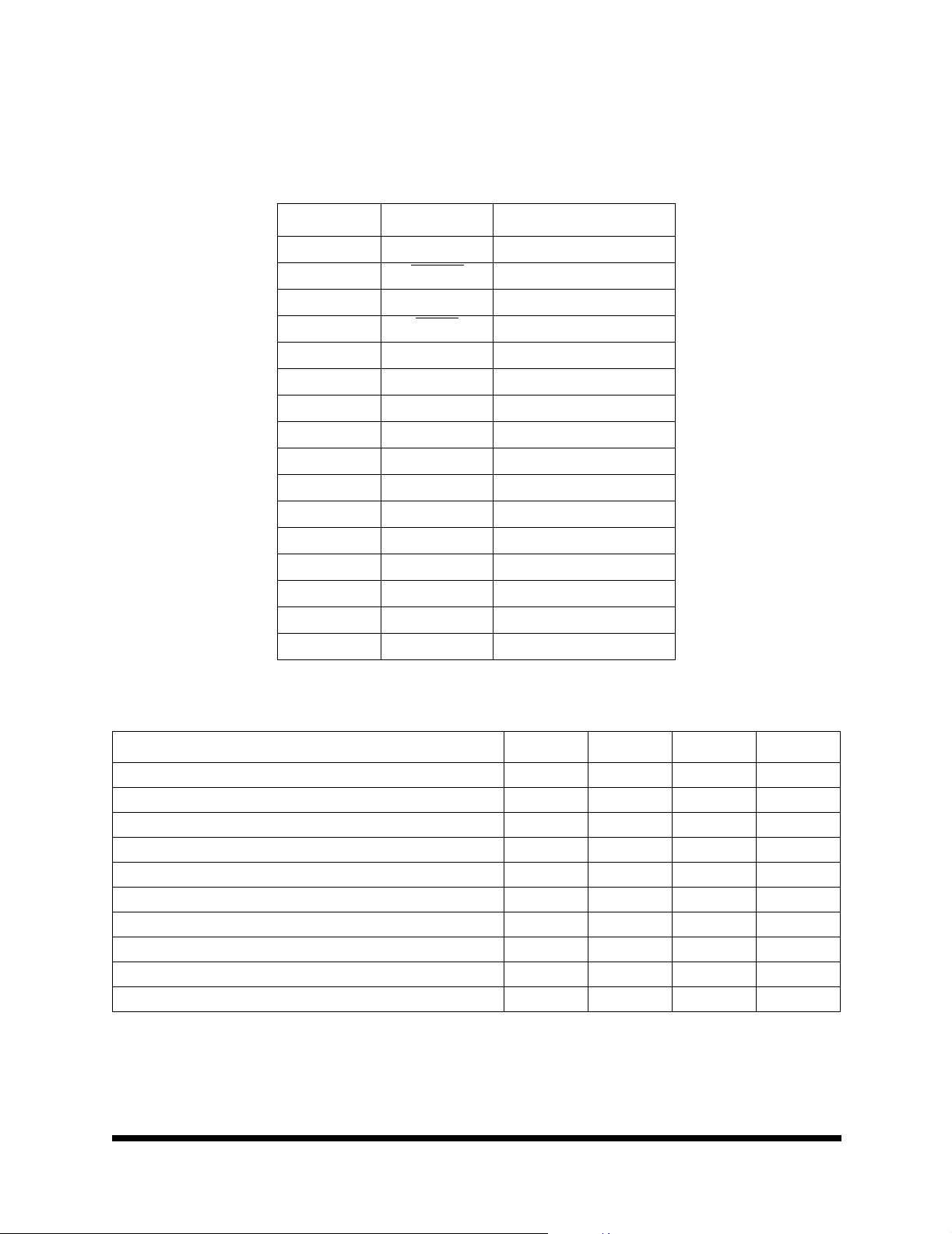
TABLE 2. 7872 ABSOLUTE MAXIMUM RATINGS
PARAMETER SYMBOL MIN MAX UNIT
Positive Supply Voltage; Relative to GND V
Negative Supply Voltage; Relative to GND V
DD
SS
AGND to DGND; Relative to GND -- -0.3 V
REF
, C
OUT
V
to AGND -- VSS -0.3 VDD +0.3 V
IN
Digital Input Voltage V
Digital Output Voltage V
Thermal Impedance
Storage Temperature Range T
Operating Temperature Range T
to AGND -- 0 V
REF
IN
OUT
Θ
JC
S
A
-0.3 7.0 V
0.3 7.0 V
+0.3 V
DD
DD
-0.3 VDD +0.3 V
-0.3 VDD +0.3 V
-- 2.44 °C/W
-65 150 °C
-55 125 °C
V
Memory
12.19.01 Rev 4
All data sheets are subject to change without notice
©2001 Maxwell Technologies
All rights reserved.
2
14-Bit A/D Converter
7872
TABLE 3. 7872 DC ELECTRICAL CHARACTERISTICS FOR DYNAMIC PERFORMANCE
(VDD = 5 V ± 5%, VSS = -5 V ± 5%, AGND = DGND = 0 V, f
P
ARAMETER SYMBOL MIN TYP MAX UNIT
Signal to Noise Ratio VIN = 10kHz Sine Wave , T
T
;
MAX
SNR is typically 82dB for V
Total Harmonic Distortion V
< 41.5kHz
IN
= 10kHz Sine Wave THD -- -86 -- dB
IN
2
MIN
to
= 2 MHZ EXTERNAL, f
CLK
SPECIFIED)
= 83 KHZ, -55 TO 125 °C UNLESS OTHERWISE
SAMPLE
SNR 79 -- -- dB
1
Peak Harmonic or Spurious Noise -- -- -86 -- dB
Intermodulation Distortion
Second Order T erms: f
= 9 kHz, fb = 9.5 kHz, f
a
= 50 kHz
Third Order Terms: f
= 9 kHz, fb = 9.5 kHz, f
a
SAMPLE
SAMPLE
IMD
--
--
-86
-86
--
--
=
50 kHz
Track/Hold Acquisition Time -- -- -- 2 µs
1. V
= ± 3 V. Guaranteed by design.
IN
2. SNR calculation includes distortion and noise components.
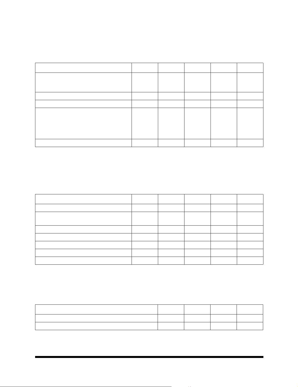
TABLE 4. 7872 DC ELECTRICAL CHARACTERISTICS FOR ACCURACY
(VDD = 5V ±5%, VSS = -5 V ± 5%, TA = -55 TO 125 °C UNLESS OTHERWISE SPECIFIED)
dB
Memory
P
ARAMETER SYMBOL MIN TYP MAX UNIT
Resolution -- 14 -- -- Bits
Resolution for Which No Missing Codes are Guaran-
-- 14 -- -- Bits
teed
°
Integral Nonlinearity @ 25
Integral Nonlinearity T
C----±1--LSB
MIN
to T
MAX
-- -- -- ±2 LSB
Bipolar Zero Error -- -- -- ±12 LSB
Positive Gain Error
Negative Gain Error
1
1
-- -- -- ±12 LSB
-- -- -- ±12 LSB
1. Measured with respect to internal reference.
TABLE 5. 7872 DC ELECTRICAL CHARACTERISTICS FOR ANALOG INPUT
(VDD = 5V ±5%, VSS = -5 V ± 5%, TA = -55 TO 125 °C UNLESS OTHERWISE SPECIFIED)
P
ARAMETER SYMBOL MIN MAX UNITS
Input Voltage Range -- -3 3 V
Input Current -- -500 500 µA
12.19.01 Rev 4
All data sheets are subject to change without notice
©2001 Maxwell Technologies
All rights reserved.
3
14-Bit A/D Converter
TABLE 6. 7872 DC ELECTRICAL CHARACTERISTICS FOR REFERENCE OUTPUT
(VDD = 5V ±5%, VSS = -5 V ± 5%, TA = -55 TO 125 °C UNLESS OTHERWISE SPECIFIED)
P
ARAMETER SYMBOL MIN MAX UNIT
REF
@ +25 °C -- 2.99 3.01 V
OUT
REF
REF
Reference Load Sensitivity (DREF
Change (0-300 µA); Reference Load Should Not Be Changed During Conversion
P
ARAMETER SYMBOL MIN MAX UNIT
to T
OUT TMIN
Tempco: Typically 35ppm -- -- ±40 ppm/oC
OUT
MAX
/DI) Reference Load Current
OUT
-- 2.98 3.02 V
-- -- 1.2 mV
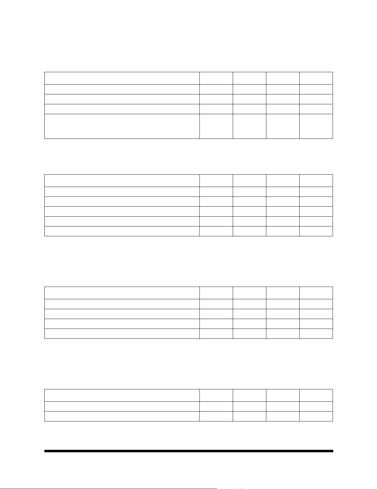
TABLE 7. 7872 DC ELECTRICAL CHARACTERISTICS FOR LOGIC INPUTS
(VDD = 5V ±5%, VSS = -5 V ± 5%, TA = -55 TO 125 °C UNLESS OTHERWISE SPECIFIED)
7872
Input High Voltage: VDD 5 V ± 5% V
Input Low Voltage: V
Input Current: V
5 V ± 5% V
DD
= 0 V to V
IN
DD
INH
I
INL
IN
2.4 -- V
-- 0.8 V
-10 10 µA
Input Current: (14/8/CLK input only) VIN = VSS to VDD -- -10 10 µA
Input Capacitance
1
C
IN
-- 10 pF
1. Not tested.
TABLE 8. 7872 DC ELECTRICAL CHARACTERISTICS FOR LOGIC OUTPUTS
(VDD = 5V ±5%, VSS = -5 V ± 5%, TA = -55 TO 125 °C UNLESS OTHERWISE SPECIFIED)
P
ARAMETER SYMBOL MIN MAX UNIT
Output High Voltage I
Output Low Voltage I
Floating-State Leakage Current -- -- 10 µA
Floating-State Output Capacitance
1. Not tested.
= 40 µA V
SOURCE
= 1.6 mA V
SINK
1
OH
OL
4.0 -- V
-- 0.4 V
-- -- 15 pF
Memory
TABLE 9. 7872 DC ELECTRICAL CHARACTERISTICS FOR CONVERSION TIME
(VDD = 5V ±5%, VSS = -5 V ± 5%, TA = -55 TO 125 °C UNLESS OTHERWISE SPECIFIED)
P
ARAMETER SYMBOL MIN MAX UNIT
External Clock -- -- 10 µs
Internal Clock: Nominal Value = 2 MHz -- -- 11 µs
12.19.01 Rev 4
All data sheets are subject to change without notice
©2001 Maxwell Technologies
All rights reserved.
4
 Loading...