

MAXWELL 7809LPRPFK, 7809LPRPFI, 7809LPRPFH, 7809LPRPFE Datasheet
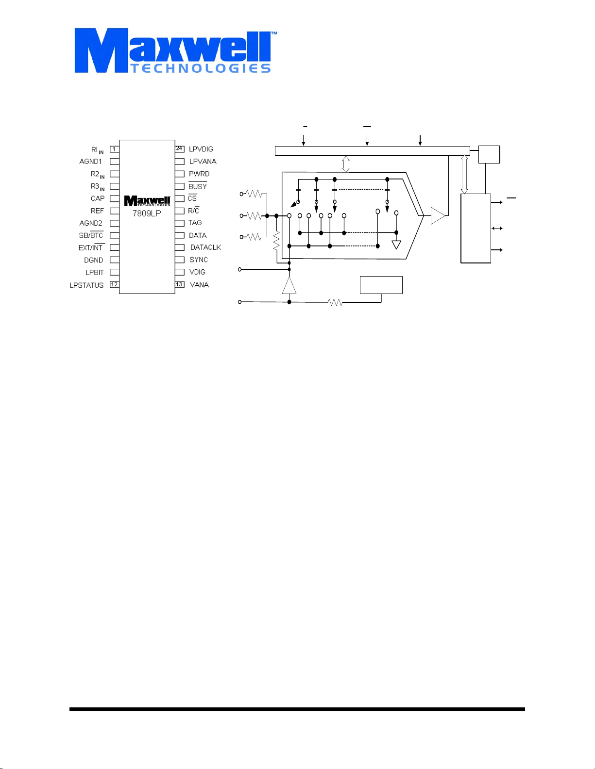
16-Bit Latchup Protected
Analog to Digital Converter
R/C CS POWER DOWN
7809LP
20 k
Ω
R1
IN
10 k
Ω
R2
IN
5 k
Ω
R3
IN
CAP
REF
20 k
Ω
FEATURES:
•RAD-PAK® radiation-hardened against natural space radia-
tion
• Total dose hardness:
- > 100 krad (Si), depending upon space mission
• Latch-up Protection Technology (LPT
• SEL converted into a reset
- Rate based on cross section and mission
• Same footprint as ADS7809
• Package: 24 pin R
AD-PAK flat package
• 100 kHz min sampling rate
• ±10 V and 0 V to 5 V input range
• Advanced CMOS technology
• DNL: 15-bits “No Missing Codes”
• 83 dB min SINAD with 20 kHz input
• Single +5 V supply operation
• Utilizes internal or external reference
• Serial output
• Power dissipation: 132 mW max
TM
)
Buffer
Successive Approximation Register and Control Logic
CDAC
Comparator
Internal
4 k
Ω
+2.5V Ref.
Clock
Serial Data
Out
Logic Diagram
DESCRIPTION:
Maxwell Technologies’ 7809LP high-speed 16-bit analog to
digital converter features a greater than 100 kilorad (Si) total
dose tolerance depending upon space mission. Using Maxwell’s radiation-hardened R
7809LP has the same footprint as ADS7809 and is latchup
protected by Maxwell Technologies’ Latchup Protection Technology (LPT
TM
). It is a 24 pin, 16-bit sampling analog-to-digital
converter using state-of-the-art CMOS structures. The
7809LP contains a 16-bit capacitor based SAR A/D with S/H,
reference, clock, interface for microprocessor use, and serial
output drivers. The 7809LP is specified at a 100kHz sampling
rate, and guaranteed over the full temperature range. Lasertrimmed scaling resistors provide various input ranges include
±10 V and 0 to 5 V, while the innovative design allows operation from a single +5 V supply, with power dissipation of under
132 mW.
Maxwell Technologies' patented R
ogy incorporates radiation shielding in the microcircuit package. It eliminates the need for box shielding while providing
the required radiation shielding for a lifetime in orbit or space
mission. In a GEO orbit, R
krad (Si) radiation dose tolerance. This product is available
with screening up to Class K.
AD-PAK® packaging technology, the
AD-PAK packaging technol-
AD-PAK provides greater than 100
BUSY
Data
Clock
Serial
Data
Memory
1000585
(858) 503-3300- Fax: (858) 503-3301 - www.maxwell.com
12.19.01 Rev 3
All data sheets are subject to change without notice
©2001 Maxwell Technologies
All rights reserved.
1
16-Bit Latchup Protected Analog to Digital Converter
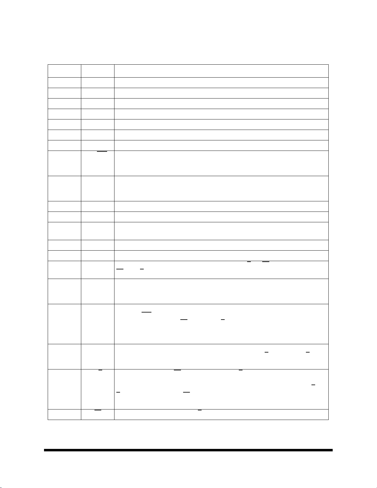
TABLE 1. 7809LP PIN DESCRIPTION
PIN SYMBOL DESCRIPTION
1 R1IN Analog Input.
2 AGND1 Analog Ground. Used internally as ground reference point.
3 R2IN Analog Input.
4 R3IN Analog Input.
5 CAP Reference Buffer Capacitor. 2.2 µF tantalum to ground.
6 REF Reference Input/Output. 2.2 µF tantalum capacitor to ground.
7 AGND2 Analog Ground.
8 SB/BTC
9 EXT/INT Select External or Internal Clock for transmitting data. If HIGH, data will be output synchronized
Select Straight Binary or Binary Two’s Complement data output format. If HIGH, data will be
output in a Straight Binary format. If LOW, data will be output in a Binary Two’s Complement
format.
to the clock input on DATACLK. If LOW, a convert command will initiate the transmission of the
data from the previous conversion, along with 16 clock pulses output on DATACLK.
7809LP
Memory
10 DGND Digital Ground.
11 LPBIT Built In test function of the latchup protection. Drive LOW during normal operation.
12 LPSTATUS Latchup Protection Status Output. LPSTATUS when HIGH indicates latchup protection is
active and output data is invalid.
13 VANA Analog Supply Input. Nominally 5V.
14 VDIG Digital Supply Input. Nominally 5V.
15 SYNC Sync Output. If EXT/INT is HIGH, either a rising edge on R/C
CS
with R/C HIGH will output a pulse on SYNC synchronized to the external DATACLK.
16 DATACLK Either an input or an output depending on the EXT/INT level. Output data will be synchronized
to this clock. If EXT/INT is LOW, DATACLK will transmit 16 pulses after each conversion, and
then remain LOW between conversions.
17 DATA Serial Data Output. Data will be synchronized to DATACLK, with the format determined by the
level of SB/BTC
level input of TAG as long as CS
on both the rising and falling edges of DATACLK, and between conversions DATA will stay at
the level of the TAG input when the conversion was started.
18 TAG Tag input for use in external clock mode. If EXT/INT is HIGH, the digital data input on TAG will
be output on DATA with a delay of 16 DATACLK pulses as long as C
HIGH.
19 R/C
20 CS
Read/Convert Input. With CS LOW, a falling edge on R/C puts the internal sample/hold into the
hold state and starts a conversion. When EXT/INT is LOW, this also initiates the transmission
of the data results from the previous conversion. If EXT/INT is HIGH, a rising edge on R/C
C
S LOW, or a falling edge on CS with R/C HIGH, transmits a pulse on SYNC and initiates the
transmission of data from the previous conversion.
Chip Select. Internally OR’ed with R/C.
. In the external clock mode, after 16-bits of data, the 7809LOPO will output the
is LOW and R/C is HIGH. If EXT/INT is LOW, data will be valid
with CS LOW or a falling edge on
S is LOW and R/C is
with
1000585
12.19.01 Rev 3
All data sheets are subject to change without notice
©2001 Maxwell Technologies
All rights reserved.
2
16-Bit Latchup Protected Analog to Digital Converter
7809LP
TABLE 1. 7809LP PIN DESCRIPTION
PIN SYMBOL DESCRIPTION
21 BUSY Busy Output. Falls when a conversion is started, and remains LOW until the conversion is com-
pleted and the data is latched into the output shift register. CS
BUSY
rises, or another conversion will start without time for signal acquisition.
or R/C must be HIGH when
22 PWRD Power Down Input. If HIGH, conversions are inhibited and power consumption is significantly
reduced. Results from the previous conversions are maintained in the output shift register.
23 LPVANA Latchup Protection Analog Supply.
24 LPVDIG Latchup Protection Digital Supply.
TABLE 2. 7809LP ABSOLUTE MAXIMUM RATINGS
PARAMETER SYMBOL MIN MAX UNIT
Analog Inputs R1
R2
R3
CAP
REF
IN
IN
IN
1
-25
-25
-25
V
+ 0.3
ANA
25
25
25
AGND2 - 0.3
Ground Voltage Differences: DGND, AGND2 -0.3 0.3 V
V
ANA
V
DIG
V
to V
DIG
ANA
-- 7 V
7V
-- 0.3 V
Specified Performance -40 85
Digital Inputs -0.3 V
Storage Temperature T
1. Indefinite short to AGND2, momentarily short to V
ANA
.
STG
-65 150
+ 0.3 V
DIG
TABLE 3. 7809LP DC ACCURACY SPECIFICATIONS
(SPECIFIED PERFORMANCE -40 TO +85°C)
P
ARAMETER MIN TYP MAX UNIT
Integral Linearity Error
-40 to 85°C
Differential Linearity Error
-40 to 85°C
No Missing Codes
Transition Noise
Full Scale Error
Full Scale Error
2
3
4,5
4,5
(using ext. 2.5000 V
)--±0.6%
ref
Full Scale Error Drift -- ±7 -- ppm/
--
--
--
--
--
--
--
--
±3
±5
-2, 3
-1, 6
LSB
15 -- -- Bits
-- 1.3 -- LSB
-- -- ±0.6 %
V
V
V
V
°
C
°
C
LSB
LSB
Memory
1
°
C
1000585
12.19.01 Rev 3
All data sheets are subject to change without notice
©2001 Maxwell Technologies
All rights reserved.
3
16-Bit Latchup Protected Analog to Digital Converter
7809LP
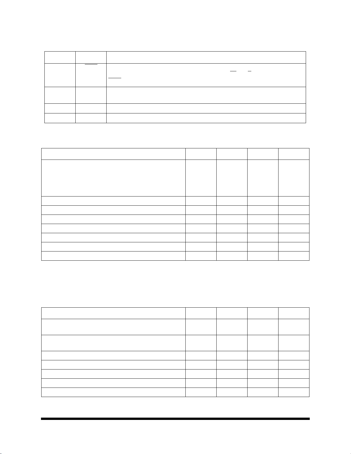
TABLE 3. 7809LP DC ACCURACY SPECIFICATIONS
(SPECIFIED PERFORMANCE -40 TO +85°C)
P
ARAMETER MIN TYP MAX UNIT
Full Scale Error Drift (using ext. 2.5000 V
Bipolar Zero Error
4
Bipolar Zero Error Drift -- ±2 -- ppm/
Unipolar Zero Error
4
-40 to 85°C
Unipolar Zero Error Drift -- ±2 -- ppm/
Recovery to Rated Accuracy after Power Down (1 uF Capacitor to
) -- ±2 -- ppm/°C
ref
-- -- ±10 mV
--
--
--
--
±3
±16
-- 1 -- ms
mV
mV
°
C
°
C
CAP)
Power Supply Sensitivity (V
-40 to 85°C
DIG
= V
= VD) 4.75 V > VD < 5.2 V
ANA
--
--
--
--
±8
±32
LSB
LSB
1. LSB stands for Least Significant Bit. One LSB is equal to 305 µV.
2. Not tested.
3. Typical rms noise at worst case transitions and temperatures.
4. Measured with various fixed resistors.
5. For bipolar input ranges, full scale error is the worst case of -Full Scale or +Full Scale untrimmed deviation from ideal first and
last scale code transitions, divided by the transition voltage (not divided by the full-scale range) and includes the effect of offset
error. For unipolar input ranges, full scale error is the deviation of the last code transition divided by the transition voltage. It
also includes the effect of offset error.
Memory
TABLE 4. 7809LP DIGITAL INPUTS
(SPECIFIED PERFORMANCE -40 TO +85°C)
P
ARAMETER MIN TYP MAX UNIT
V
IL
V
IH
IIL, I
IH
-0.3
2.0
--
--
--
--
V
0.8
+ 0.3
D
±10
TABLE 5. 7809LP ANALOG INPUT AND THROUGHPUT SPEED
(SPECIFIED PERFORMANCE -40 TO +85°C)
P
ARAMETER MIN TYP MAX UNIT
Voltage Ranges 10 V, 0 V to 5 V
Impedance
Capacitance -- 35 -- pF
Conversion Time -- 7.6 8 µs
Complete Cycle (Acquire and Convert) -- -- 10 µs
Throughput Rate
1
100 -- -- kHz
1. Tested by application of signal.
See Table 2.
V
V
µA
1000585
12.19.01 Rev 3
All data sheets are subject to change without notice
©2001 Maxwell Technologies
All rights reserved.
4
16-Bit Latchup Protected Analog to Digital Converter
7809LP
TABLE 6. 7809LP AC ACCURACY SPECIFICATIONS
(SPECIFIED PERFORMANCE -40 TO +85°C)
P
ARAMETER MIN TYP MAX UNIT
Spurious-Free Dynamic Range, fIN = 20 kHz
Total Harmonic Distortion, f
= 20 kHz
IN
Signal-to-Noise (Noise + Distortion)
1
1
fIN = 20 kHz
-60 dB Input
1
Signal-to-Noise
Full-Power Bandwidth
, fIN = 20 kHz 83 88 -- dB
1,3
1
90 100 -- dB
-- -100 -90 dB
83
--
88
30
--
--
-- 250 -- kHz
2
dB
1. Guaranteed by design.
2. All specifications in dB are referred to a full-scale ±10 V input.
3. Full-Power Bandwidth defined as Full-Scale input frequency at which Signal-to-Noise (Noise + Distortion) degrades to 60 dB.
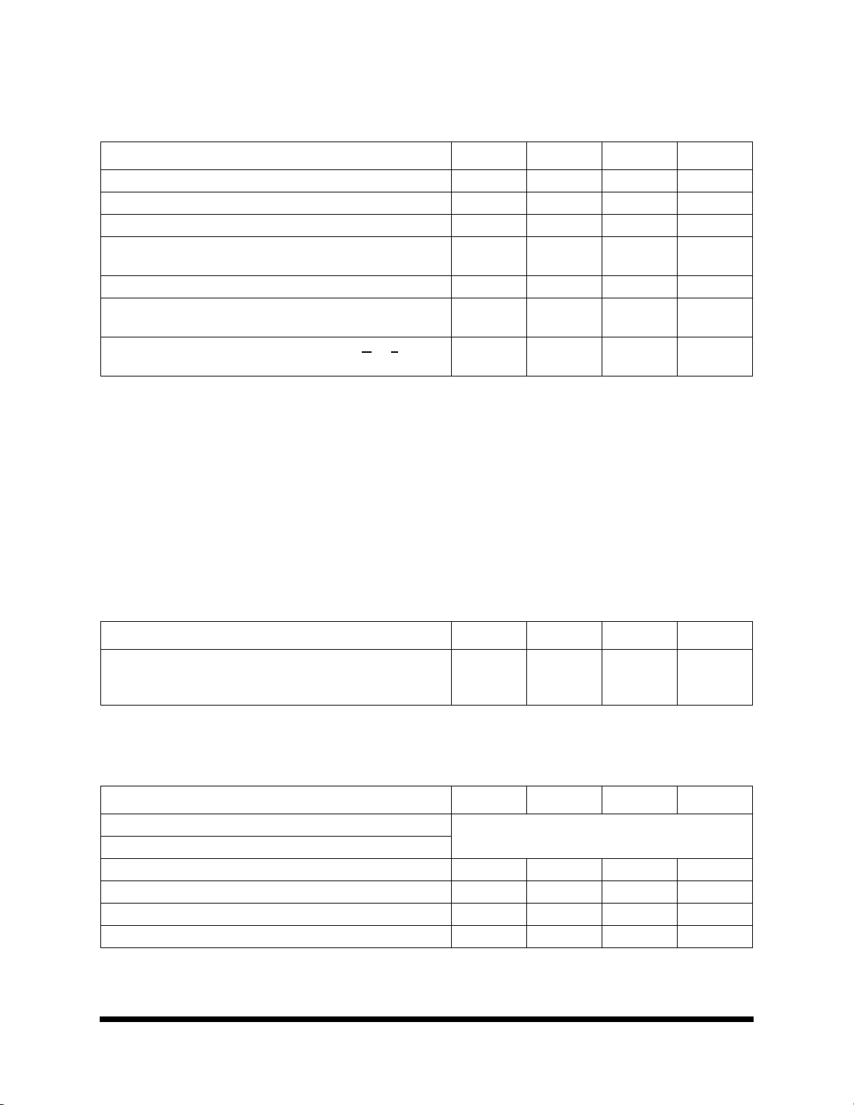
TABLE 7. 7809LP SAMPLING DYNAMICS
(SPECIFIED PERFORMANCE -40 TO +85°C)
Memory
P
ARAMETER MIN TYP MAX UNIT
Aperture Delay -- 40 -- ns
Aperture Jitter Sufficient to meet AC specification
Transient Response FS Step -- 2 -- us
Overvoltage Recovery
1
-- 150 -- ns
1. Recovers to specified performance after 2 X FS input overvoltage.
TABLE 8. 7809LP REFERENCE
(SPECIFIED PERFORMANCE -40 TO +85°C)
P
ARAMETER CONDITIONS MIN TYP MAX UNIT
Internal Reference Voltage No Load 2.48 2.5 2.52 V
Internal Reference Source Current (Must be
ext. buffer)
External Reference Voltage Range for Specified Linearity
1
External Reference Current Drain Ext. 2.5000V Ref -- -- 100 µA
1. Tested by application of signal.
-- 1 -- µA
2.3 2.5 2.7 V
1000585
12.19.01 Rev 3
All data sheets are subject to change without notice
©2001 Maxwell Technologies
All rights reserved.
5

16-Bit Latchup Protected Analog to Digital Converter
7809LP
TABLE 9. 7809LP DIGITAL OUTPUTS
(SPECIFIED PERFORMANCE -40 TO +85°C)
P
ARAMETER CONDITIONS MIN TYP MAX UNIT
Data Format
Data Coding
Pipeline Delay
Data Clock
Internal (Output Only When Transmitting
Data)
External (Can Run Continually)
V
OL
V
OH
Leakage Current
Output Capacitance
1
1
Serial 16-bits
Binary Two’s Complement or Straight Binary
Conversion results only available after completed conversion
Selectable for internal or external data clock
EXT/INT
EXT/INT
I
I
High-Z State,
V
= 1.6 mA
SINK
SOURCE
= 0V to V
OUT
Low
High
= 500 µA
DIG
--
0.1
-4
2.3
--
--
--
--
10
0.4
--
-- -- ±10 µA
High-Z State -- 15 -- pF
1. Not tested.
TABLE 10. 7809LP POWER SUPPLIES
(SPECIFIED PERFORMANCE -40 TO +85°C)
P
ARAMETER CONDITIONS MIN TYP MAX UNIT
V
DIG
V
ANA
I
DIG
I
ANA
Power Dissipation
PWRD LOW
PWRD HIGH
Must be < V
V
= V
ANA
= 100 kHz
s
DIG
f
ANA
= 5V
4.75 5 5.25 V
4.75 5 5.25 V
-- 0.3 -- mA
-- 16 -- mA
--
--
--
--
132
350
MHz
V
Memory
mW
1000585
12.19.01 Rev 3
All data sheets are subject to change without notice
©2001 Maxwell Technologies
All rights reserved.
6

16-Bit Latchup Protected Analog to Digital Converter
TABLE 11. 7809LP CONTROL LINE FUNCTIONS FOR READ AND CONVERT
7809LP
SPECIFIC FUNCTION CS R/C BUSY EXT/INT
Initiate Conversion and Output
Data using Internal Clock
Initiate Conversion and Output
Data using External Clock
Incorrect Conversions
Power Down x
1 > 0
1 > 0
1 > 0
1 > 0
0
0
0
000 > 1xx0xCS
x
0
1 > 0
0
1 > 0
1
1
0 > 1
x
x
1
1
1
1
1
0
0
x
x
0
0
1
1
1
1
1
x
x
DATACL
K
Output
Output
Input
Input
Input
Input
Input
x
x
PWRD SB/BTC
0
0
0
0
x
0
0
0
1
x
x
x
x
x
x
x
x
x
OPERATION
Initiates conversion “n”.
Data from conversion “n1” clocked out on DATA
synchronized to 16 clock
pulses output on DATACLK
Initiates conversion “n”.
Data from conversion “n1” clocked out on DATA
synchronized to 16 clock
pulses output on DATACLK
Initiates conversion “n”
Initiates conversion “n”
Outputs a pulse on SYNC
followed by data from conversion “n” clocked out
synchronized to external
DATACLK.
Outputs a pules on SYNC
followed by data from conversion “n-1” clocked out
synchronized to external
DATACLK
“n” in process.
Outputs a pulse on SYNC
followed by data from conversion “n-1” clocked out
synchronized to external
DATACLK
“n” in process.
or a new conversion will
be initiated without time
for acquisition
Analog circuitry powered.
Conversion will be initiated without time for
acquisition
Analog circuitry disabled.
Data from previous conversion maintained in output registers
1
. Conversion
1
. Conversion
or R/C must be HIGH
Memory
1000585
12.19.01 Rev 3
All data sheets are subject to change without notice
©2001 Maxwell Technologies
All rights reserved.
7
 Loading...