

MAXWELL 7805ALPRPFS, 7805ALPRPFI, 7805ALPRPFE, 7805ALPRPFB, 7805ALPRPDS Datasheet
...
1
Memory
All data sheets are subject to change without notice
(858) 503-3300 Fax: (858) 503-3301- www.maxwell.com
PRELIMINARY
16-Bit Latchup Protected ADC
7805ALP
©2001 Maxwell Technologies
All rights reserved.
12.19.01 Rev 6
1000583
FEATURES:
• 16-bit organization
• Latchup Protection Technology™
•R
AD-PAK® radiation-hardened against natural space radia-
tion
• Total dose hardness:
- > 50 krads(Si), depending upon space mission
• Latchup converted to reset.
- Rate based on cross section and mission.
• Package:
- 28 pin R
AD-PAK® flat pack
- 28 pin R
AD-PAK® DIP
• 100 kHz min sampling rate
• Standard ± 10V input range
• Advance CMOS technology
- 86 dB min SINAD with 20 kHz input
- Single 5V supply operation
- Utilizes internal or external reference
- Full parallel data output
- Power dissipation: 132 mW max
DESCRIPTION:
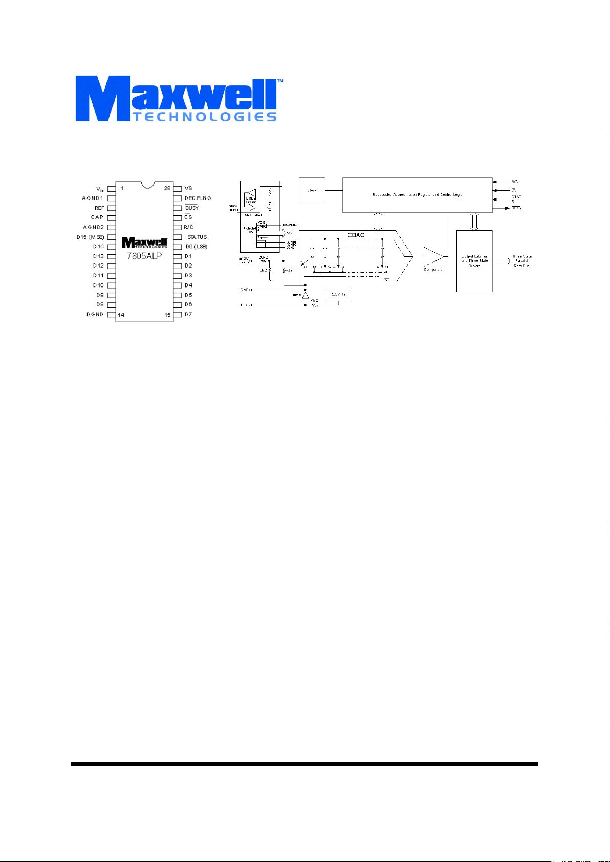
Maxwell Technologies’ 7805ALP high-speed analog-to-digital
converter features a greater than 50 krad (Si) total dose tolerance, depending upon space mission. Using Mawell’s radiation-hardened R
AD-PAK® packaging technology, the 7805ALP
incorporates the commercial ADS 7805 from Burr Brown. This
device is latchup protected by Maxwell Technologies’ LPT™
technology. The 7805ALP, 16-bit sampling A/D using state-ofthe-art CMOS structure. The device contains a complete 16bit capacitor-based SAR A/D with S/H, reference, clock, interface for microprocessor use, and three-state output drivers.
The 7805ALP is specified at a 100 kHz sampling rate, and
guaranteed over the full temperature range. Laser-trimmed
scaling resistors provide an industry-standard ± 10V input
range, while the innovative design allows operation from a single 5V supply, with power dissipation of under 132 mW.
Maxwell Technologies' patented R
AD-PAK® packaging technol-
ogy incorporates radiation shielding in the microcircuit package. It eliminates the need for box shielding while providing
the required radiation shielding for a lifetime in orbit or space
mission. In a GEO orbit, R
AD-PAK provides greater than 100
krad (Si) radiation dose tolerance. This product is available
with screening up to Class S.
Logic Diagram

Memory
PRELIMINARY
2
All data sheets are subject to change without notice
©2001 Maxwell Technologies
All rights reserved.
16-Bit Latchup Protected ADC
7805ALP
12.19.01 Rev 6
1000583
TABLE 1. 7805ALP PINOUT DESCRIPTION
PIN NUMBER NAME DIGITAL I/O DESCRIPTION
1V
IN
Analog input.
2 AGND1 Analog ground. Used internally as ground reference point.
3 REF Reference input/output. 2.2 µF tantalum capacitor to ground
4 CAP Reference buffer capacitor. 2.2 µF tantalum capacitor to ground.
5 AGND2 Analog ground.
6 D15 (MSB) 0 Data bit 15. Most Significant Bit (MSB) of conversion results. When STATUS is
HIGH*, D15 must not be driven high.
7 D14 0 Data bit 14. When STATUS is HIGH*, D14 must not be driven high.
8 D13 0 Data bit 13. When STATUS is HIGH*, D13 must not be driven high.
9 D12 0 Data bit 12. When STATUS is HIGH*, D12 must not be driven high.
10 D11 0 Data bit 11. When STATUS is HIGH*, D11 must not be driven high.
11 D10 0 Data bit 10. When STATUS is HIGH*, D10 must not be driven high.
12 D9 0 Data bit 9. When STATUS is HIGH*, D9 must not be driven high.
13 D8 0 Data bit 8. When STATUS is HIGH*, D8 must not be driven high.
14 DGND Digital Ground
15 D7 0 Data bit 7. When STATUS is HIGH*, D7 must not be driven high.
16 D6 0 Data bit 6. When STATUS is HIGH*, D6 must not be driven high.
17 D5 0 Data bit 5. When STATUS is HIGH*, D5 must not be driven high.
18 D4 0 Data bit 4. When STATUS is HIGH*, D4 must not be driven high.
19 D3 0 Data bit 3. When STATUS is HIGH*, D3 must not be driven high.
20 D2 0 Data bit 2. When STATUS is HIGH*, D2 must not be driven high.
21 D1 0 Data bit 1. When STATUS is HIGH*, D1 must not be driven high.
22 D0 (LSB) 0 Data bit 0. Least Significant Bit (LSB) of conversion results. When STATUS is
HIGH*, D0 must not be driven high.
23 STATUS* 0 STATUS when HIGH indicates latchup protection is active and output data is
invalid. Capacitive loading should not exceed 1000 pF.
24 R/C
IWith CS LOW and BUSY HIGH, a falling edge of R/C initiates a new conversion.
When STATUS is HIGH*, CS
and R/C must not be driven high.
25 CS
I Internally OR’d with R/C. If R/C LOW, a falling edge on CS initiates a new conver-
sion. When STATUS is HIGH*, CS
and R/C must not be driven high.
26 BUSY
0 At the start of a conversion, BUSY goes LOW and stays LOW until the conversion
is completed and the digital outputs have been updated.
27 DECPLNG Supply voltage high speed decoupling pin. Decouple to ground with 1.0 µF ceramic
capacitor.
28 V
S
Supply input. Nominally 5V. Decouple to ground with 10 µF tantalum capacitor.

Memory
PRELIMINARY
3
All data sheets are subject to change without notice
©2001 Maxwell Technologies
All rights reserved.
16-Bit Latchup Protected ADC
7805ALP
12.19.01 Rev 6
1000583
TABLE 2. 7805ALP ABSOLUTE MAXIMUM RATINGS
PARAMETER SYMBOL MIN TYP MAX UNIT
Analog Inputs V
IN
CAP
REF
-25
V
S
9
--
--
--
25
AGND2 - 0.3
--
V
Ground Voltage Difference DGND
AGND1
AGND2
-0.3
-0.3
-0.3
--
--
--
0.3
0.3
0.3
V
Supply Input V
S
-- 7 V
Digital Inputs -0.3 -- VS + 0.3 V
Internal Power Dissipation -- -- 825 mW
Maximum Junction Temperature T
J
-- -- 165
°
C
TABLE 3. 7805ALP DC ACCURACY SPECIFICATIONS
PARAMETER CONDITIONS MIN TYP MAX UNIT
Integral Linearity Error -- -- ±3 LSB
Differential Linearity Error -- -- 4, -1 LSB
No Missing Codes
1
1. Not tested.
15 -- -- Bits
Transition Noise
2
2. Typical rms noise at worst case transitions and temperatures.
-- 1.3 -- LSB
Full Scale Error
3,4
3. Measured with various fixed resistors.
4. Full scale error is worst case - Full Scale or +Full Scale untrimmed deviation from ideal first and last code transitions, divided
by the transition voltage (not divided by the full-scale range) and included the effect of offset error.
-- -- ±0.5 %
Full Scale Error Drift -- ±7 -- ppm/
°
C
Bipolar Zero Error
3
-- -- ±10 mV
Bipolar Zero Error Drift -- ±2 -- ppm/
°
C
Power Supply Sensitivity 4.8V < V
S
< 5.25V -- -- ±8 LSB
TABLE 4. 7805ALP DIGITAL INPUTS
PARAMETER MIN TYP MAX UNIT
V
IL
-0.3 -- 0.8 V
V
IH
2.0 -- VS +0.3 V
I
IL
, I
IH
-- -- ±10 µA

Memory
PRELIMINARY
4
All data sheets are subject to change without notice
©2001 Maxwell Technologies
All rights reserved.
16-Bit Latchup Protected ADC
7805ALP
12.19.01 Rev 6
1000583
TABLE 5. 7805ALP ANALOG INPUTS
PARAMETER MIN TYP MAX UNIT
Voltage Ranges
1
1. Tested by application of signal.
-10 ±10 10 V
Impedance -- 23 -- k
Ω
Capacitance -- 35 -- pF
TABLE 6. 7805ALP THROUGHPUT SPEED
PARAMETER MIN TYP MAX UNIT
Conversion Time -- 7.6 8 µs
Complete Cycle (Acquire and Convert) -- -- 10 µs
Throughput Rate
1
1. Not tested.
100 -- -- kHz
TABLE 7. 7805ALP AC ACCURACY SPECIFICATIONS
PARAMETER TEST CONDITIONS MIN TYP MAX UNIT
Spurious-Free Dynamic Range
1,2
1. All specifications in dB are referred to a full-scale 10V input.
2. Guaranteed by design.
f
IN
= 45 kHz 90 -- -- dB
Total Harmonic Distortion
1,2
f
IN
= 45 kHz -- -- -90 dB
Signal-to-(Noise + Distortion)
1,2
f
IN
= 45 kHz 83 -- -- dB
-60dB Input -- 30 --
Signal-to-Noise
1,2
f
IN
= 45 kHz 83 -- -- dB
Full-Power Bandwidth
3
3. Full-power bandwidth defined as full-scale input frequency at which signal-to-(noise + distortion) degrades to 60 dB or 10 bits
of accuracy.
-- 250 -- kHz
TABLE 8. 7805ALP SAMPLING DYNAMICS
PARAMETER TEST CONDITIONS MIN TYP MAX UNIT
Aperture Delay -- 40 -- nS
Transient Response FS Step -- 2 -- µS
Overvoltage Recovery
1
1. Recovers to specified performance after 2 x fS input overvoltage.
-- 150 -- nS

Memory
PRELIMINARY
5
All data sheets are subject to change without notice
©2001 Maxwell Technologies
All rights reserved.
16-Bit Latchup Protected ADC
7805ALP
12.19.01 Rev 6
1000583
TABLE 9. 7805ALP REFERENCE
PARAMETER MIN TYP MAX UNIT
Internal Reference Voltage 2.48 2.5 2.52 V
Internal Reference Source Current (Must use external buffer) -- 1 -- µA
Internal Reference Drift -- 8 -- ppm/
°
C
External Reference Voltage Range for Specified Linearity
1
1. Tested by application of signal.
-- 2.5 -- V
External Reference Current Drain
2
2. Not tested.
-- -- 100 µA
TABLE 10. 7805ALP DIGITAL OUTPUTS
PARAMETER TEST CONDITIONS MIN TYP MAX UNIT
Data Formatting (Parallel 16-bits Binary Two’s Complement)
Data Coding Binary Two’s Complement
V
OL
(I
SINK
= 1.6mA) 4.0 -- -- 0.4 V
V
OH
(I
SOURCE
= -400 µA) 4.0 -- -- V
Leakage Current High-Z State, V
OUT
= 0V
to V
S
-- -- ±5 µA
Output Capacitance High-Z State -- 10 -- pF
TABLE 11. 7805ALP POWER SUPPLIES
PARAMETER TEST CONDITIONS MIN TYP MAX UNIT
V
S
4.8 5 5.25 V
I
S
-- 20.3 -- mA
Power Dissipation f
S
= 100 kHz -- 102 132.0 mW
TABLE 12. 7805ALP DIGITAL TIMING
PARAMETER MIN TYP MAX UNIT
Bus Access Time -- -- 83 nS
Bus Relinquish Time -- -- 83 nS
Memory
PRELIMINARY
6
All data sheets are subject to change without notice
©2001 Maxwell Technologies
All rights reserved.
16-Bit Latchup Protected ADC
7805ALP
12.19.01 Rev 6
1000583
TABLE 13. 7805ALP TEMPERATURE
PARAMETER MIN TYP MAX UNIT
Specified Performance -40 -- 85
°
C
Derated Performance
1
1. Tested by application of signal.
-55 -- 125
°
C
Storage -65 -- 150
°
C
TABLE 14. 7805ALP CONVERSION TIMING
1
1. Tested by application of signal.
D
ESCRIPTION SYMBOL MIN TYP MAX UNIT
Convert pulse width t
1
40 -- 7000 ns
Data valid delay after R/C
low t
2
-- -- 8 µs
BUSY
delay from R/C low t
3
-- -- 85 ns
BUSY
low t
4
-- -- 8 µs
BUSY
delay after end-of-conversion t
5
-- 220 -- ns
Aperture time t
6
-- 40 -- ns
Conversion time t
7
-- 7.6 8 µs
Acquisition time t
8
-- -- 2 µs
Bus relinquish time t
9
10 35 83 ns
BUSY
delay after data valid t
10
50 200 -- ns
Previous data valid delay after R/C
low t
11
-- 7.4 -- µs
Throughput time t
7
+ t
8
-- 9 10 µs
R/C
to CS setup time t
12
10 -- -- ns
Time between conversions t
13
10 -- -- µs
Bus access time t
14
10 -- 83 ns
TABLE 15. 7805ALP CONTROL LINE FUNCTION FOR READ AND CONVERT
CS R/C BUSY OPERATION
1 X X None. Databus is in Hi-Z state.
↓ 0 1 Initiates conversion "n". Databus remains in Hi-Z state.
0
↓ 1 Initiates conversion "n". Databus enters Hi-Z state.
01
↓ Conversion "n" completed. Valid data from conversion "n" on the databus.
↓ 1 1 Enables databus with valid data from conversion "n".
↓ 1 0 Enables databus with valid data from conversion "n-1". Conversion "n" in progress.

Memory
PRELIMINARY
7
All data sheets are subject to change without notice
©2001 Maxwell Technologies
All rights reserved.
16-Bit Latchup Protected ADC
7805ALP
12.19.01 Rev 6
1000583
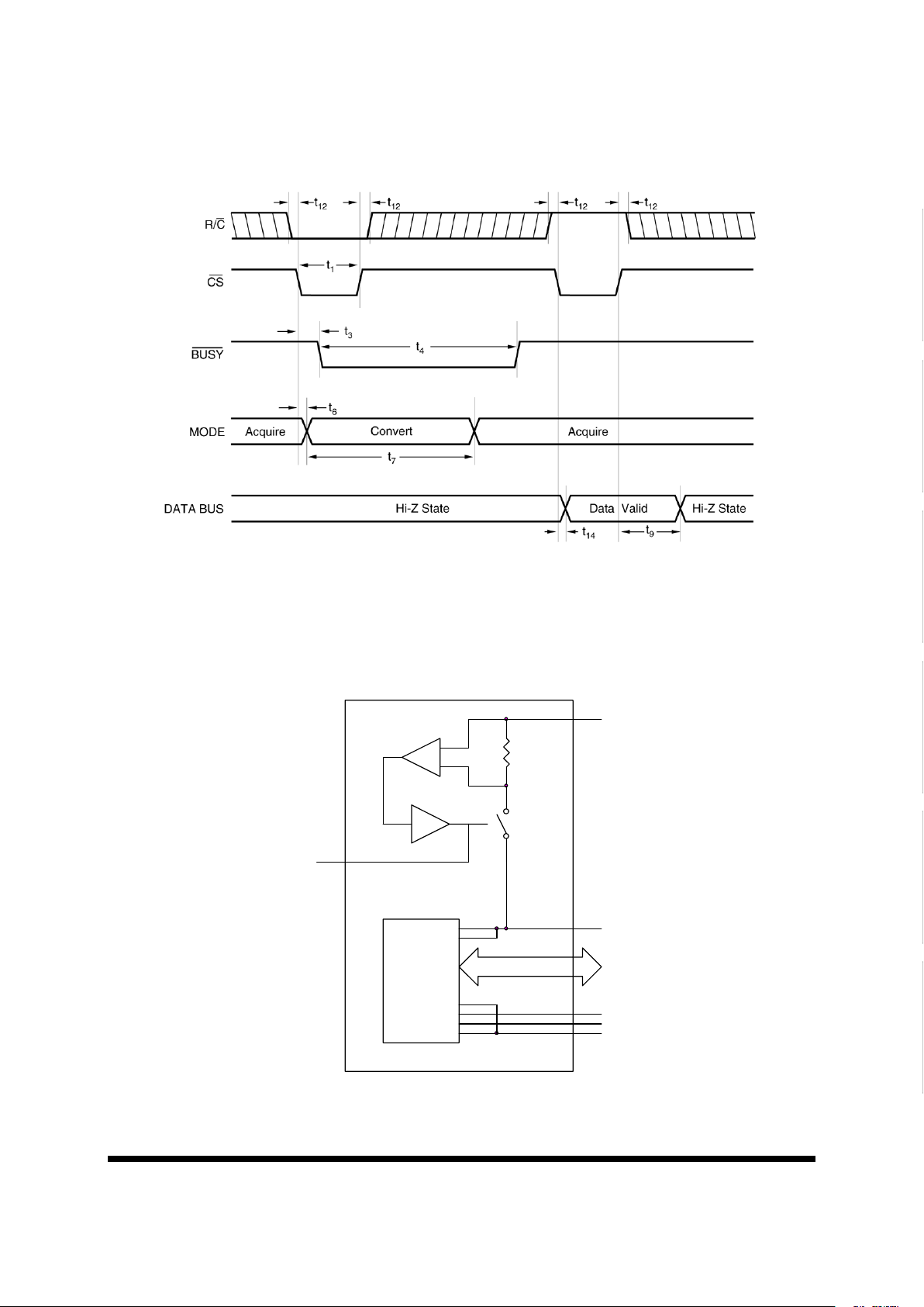
FIGURE 1. CONVERSION TIMING WITH OUTPUTS ENABLED AFTER CONVERSION (CS TIED LOW)
0 ↓ 0 Enables databus with valid data from conversion "n-1". Conversion "n" in
progress."
00
↓ New conversion initiated without acquisition of a new signal. Data will be invalid.
CS
and/or R/C must be HIGH when BUSY goes HIGH.
X X 0 New convert commands ignored. Conversion "n" in progress.
TABLE 15. 7805ALP CONTROL LINE FUNCTION FOR READ AND CONVERT
CS R/C BUSY OPERATION
Memory
PRELIMINARY
8
All data sheets are subject to change without notice
©2001 Maxwell Technologies
All rights reserved.
16-Bit Latchup Protected ADC
7805ALP
12.19.01 Rev 6
1000583
FIGURE 2. USING CS TO CONTROL CONVERSION AND READ TIMING
LPT™ Operation
Latchup Protection Technology (LPT
™) automatically detects an increase in the supply current of the 7805ALP con-
verter due to a single event effect and internally cycles the power to the converter off, then on, which restores the
steady state operation of the device. A simplified block diagram of the 7805ALP circuitry is shown in Figure 1. The circuitry consists of a protected device, the ADS7805 die, a current sensor, a power switch, and a status output driver.
FIGURE 3. LATCHUP PROTECTION DIAGRAM
VS
I/Os
POWER
SWITCH
PROTECTED
DEVICE
STATUS
OUTPUT
DECPLNGVDIG
VANA
BYTE
ADS7805
7805ALPRP
DGND
AGND2
AGND1
CURRENT
SENSOR
STATUS
DRIVER

Memory
PRELIMINARY
9
All data sheets are subject to change without notice
©2001 Maxwell Technologies
All rights reserved.
16-Bit Latchup Protected ADC
7805ALP
12.19.01 Rev 6
1000583
Differences Between the7805A and the ADS7805
Because the 7805A uses the ADS7805 die to perform the analog to digital conversion function its operation and performance is very similar to the ADS7805 packaged part from Burr-Brown. In general the operation and application will
be the same for both parts. There are two primary differences: the operation of the supply pins and the operation of the
BYTE and STATUS pins.
The ADS7805 provides separate analog and digital supply pins. The 7805A provides a single supply input V
S
pin in
place of the V
DIG
pin which powers both the analog and digital circuitry through the LPT™ current sensor and power
switch. The V
S
power supply should be treated as an analog supply and isolated from noise on the system digital
power supply. The low side of the power switch connects to the ADS7805 die power pads and to the package DECPLNG pin which replaces the VANA pin. The DECPLNG pin allows low ESR ceramic capacitors to directly decouple
the ADS7805 die. CAUTION: The DECPLNG pin must not be connected to the power supply since this will defeat the
LPT
™ power switch and could result in latchup of the device during operation in a radiation environment. Electrolytic
capacitors should not be connected to the DECPLNG pin because the large capacitance will increase the recovery
time of the 7805A.
The primary functional difference between the ADS7805 and the 7805A is that the BYTE signal of the ADS7805 is
internally grounded and the pin function is replaced by the STATUS output. Grounding the BYTE signal permanently
assigns the data output signal bits 15:0 as shown in the 7805A pinout diagram where bit15 is the MSB and bit 0 is the
LSB.
A high level STATUS signal indicates that a single event induced latchup current was detected by the LPT
™ circuitry
causing power to be removed from the protected device. CAUTION: During the time that power is removed from the
protected device, it is critical that external circuitry driving the device I/O pins does not backdrive the device supply.
Backdriving the supply could contribute to an extended or even a permanent latchup condition.
In order to prevent backdriving the supply, the STATUS signal should be used in the system to tri-state or gate external
I/O drive circuits to a low state. Similarly, if the data outputs are connected to a bus with other bus driver circuits, all
external data bus drivers must be tri-stated and individual pull up resistors to the supply voltage (if used on the data
bus) must not be less than 10 K
Ω typical to assure proper single event effect recovery. Tri-stating of inputs should
occur within 100 nsec after the rise of the status pin. The BYTE signal can be made available in place of the STATUS
signal at customer request.
STATUS can also be used to generate an input to the system data processor indicating that an LPT
™ cycle has
occurred, and the protected device output accuracy may not be met until after the respective recovery time to the
event. The STATUS signal is generated from an advanced CMOS logic gate output. This output may not exhibit a
monotonic falltime and may even oscillate briefly while power is being restored to the protected device and the decoupling capacitance is charged. Loading on the STATUS output should be minimized because this signal is used internally by the 7805A. It is recommended that load current not exceed 2 mA and load capacitance be kept well below
1000 pF.
A summary of the pin differences between the ADS7805 and 7805A is provided below.
TABLE 16. PIN DIFFERENCES
PIN NUMBER ADS7805 7805A PIN DIFFERENCE DESCRIPTION
23 BYTE STATUS A high level STATUS signal indicates that power is removed from the ADS7805 die.
I/O pins must not be driven high while this signal is active. The BYTE signal of the
ADS7805 die is internally grounded but can also be made available in place of the
STATUS pin at customer request.
Memory
PRELIMINARY
10
All data sheets are subject to change without notice
©2001 Maxwell Technologies
All rights reserved.
16-Bit Latchup Protected ADC
7805ALP
12.19.01 Rev 6
1000583
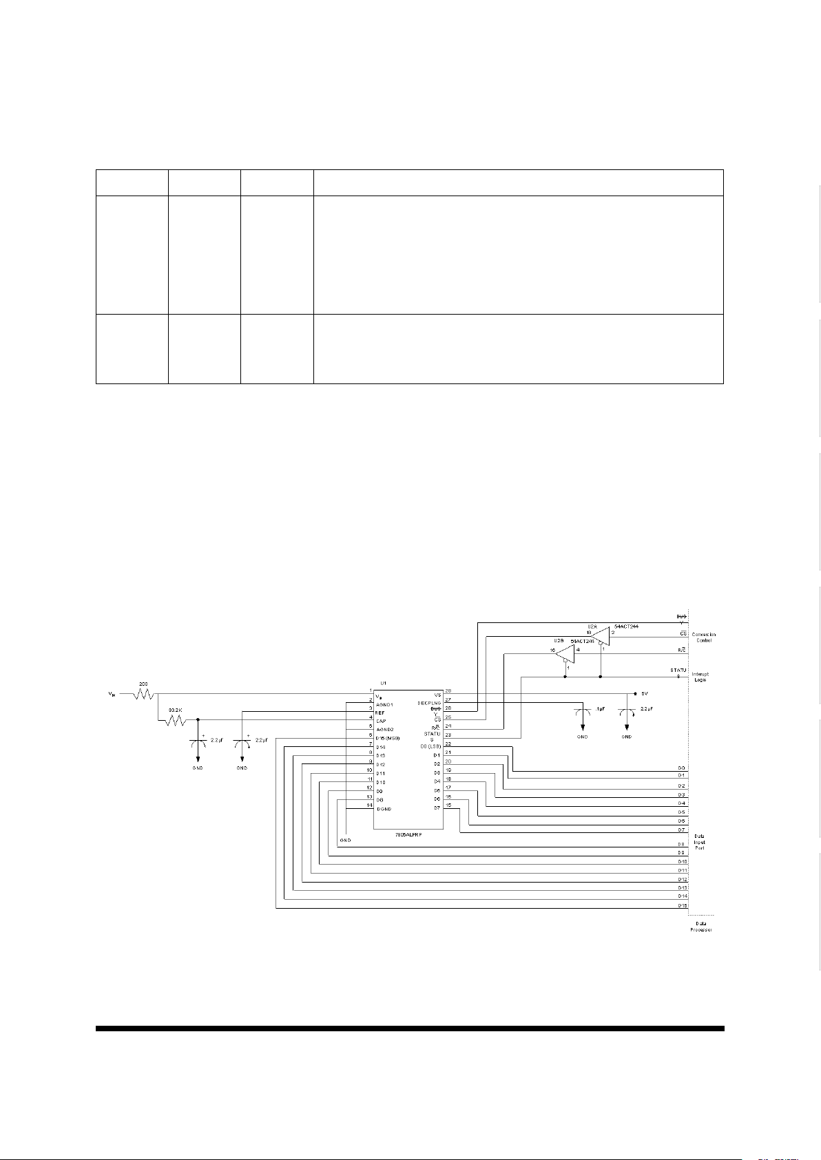
Example Circuits for Using the 7805A
Figure 2 shows a typical application circuit for using the 7805A as an input to a digital data processor. This circuit
shows the use of the STATUS pin to tri-state the control inputs when the latchup protection circuit cycles the power to
the protected ADS7805 die.
Figure 3 shows a typical application circuit for connecting the 7805A to a 16-bit data bus with multiple drivers on the
bus. Tri-state buffers are used to isolate the 7805A data outputs from the data bus. Figure 4 shows the typical application circuit for connecting the 7805A to an 8-bit data bus.
FIGURE 4. TYPICAL 7805A APPLICATION CIRCUIT
27 VANA DECPLNG The ADS7805 VANA and V
DIG
die pads are connected together and are available
at the DECPLNG pin. This pin allows external ceramic capacitors to directly decouple the power inputs to the ADS7805 die-to-analog ground. Decoupling capacitance should not exceed 0.2 uF typical. This pin must not be connected to a power
supply directly since this will defeat the latchup protection circuitry. Electrolytic filter
capacitors should not be connected to this pin but should be connected between
the V
S
pin and ground.
28 V
DIG
V
S
This is the power supply input for the LPT circuitry and the protected ADS7805 die.
This supply should be treated as an analog supply with filtering and/or isolation
from the noisy system digital power supply. The LPT latchup current sense and
power switch circuitry is located between this pin and the DECPLNG pin.
TABLE 16. PIN DIFFERENCES
PIN NUMBER ADS7805 7805A PIN DIFFERENCE DESCRIPTION

Memory
PRELIMINARY
11
All data sheets are subject to change without notice
©2001 Maxwell Technologies
All rights reserved.
16-Bit Latchup Protected ADC
7805ALP
12.19.01 Rev 6
1000583
FIGURE 5. TYPICAL 7805A CIRCUIT WITH 16-BIT BUS INTERFACE
FIGURE 6. TYPICAL 7805A CIRCUIT WITH 8-BIT BUS INTERFACE
Testing the 7805A Latchup Protection Circuitry
The DECPLNG pin provides direct access to the 7805ALP converter supply pins for attaching external decoupling
capacitor(s) to ground. This pin can also be used to test the LPT
™ operation by sinking a pulsed current load to
ground as shown in the test circuit in Figure 5 and as described in the LPT Operating Characteristics Table (Table 17)
 Loading...