


7B991
Programmable Skew
Clock Buffer (PSCB)
FEATURES:
• All output pair skew < 100 ps typical (250 max.)
• 3.75 to 80 MHz output operation
• User-selectable output functions
• Selectable skew to 18 ns
• Inverted and non-inverted
• Operation at ½ and ¼ input frequency
• Operation at 2x and 4x input frequency (input as low as
3.75 MHz)
• Zero input to output delay
• 50% duty-cycle outputs
• Outputs drive 50
• Low operating current
• Package: 32-pin R
• Jitter < 200 ps peak-to-peak (< 25 ps RMS)
• Compatible with Pentium™-based processor
• Total dose hardness:
- >100 krads (Si), depending upon space mission
• Excellent Single Event Effects:
- SEL > 116MeV/mg/cm
- SEUTH -3 MeV/mg/cm
- SEU sat cross section: 1E-3/device
Ω terminated lines
AD-PAK® flat package
2
2
Logic Diagram
DESCRIPTION:
Maxwell Technologies’ 7B991 Programmable Skew Clock
Buffers (PSCB) offer user-selectable control over system
clock functions. These multiple-output clock drivers provide
the system integrator with functions necessary to optimize timing of high-performance computer systems. Eight individual
drivers, arranged as four pairs of user-controllable outputs,
can each drive terminated transmission lines with impedances
as low as 50
skews and full-swing logic levels.
Each output can be hardwired to one of nine delay or function
configurations. Delay increments of 0.7 to 1.5 ns are determined by the operating frequency with outputs able to skew up
to ± 6 time units from their nominal “zero” skew position. The
completely integrated PLL allows external load and transmission line delay effects to be canceled. When this “zero delay”
capability of the PSCB is combined with the selectable output
skew functions, the user can create output-to-output delays of
up to ±12 time units.
Maxwell Technologies' patented R
ogy incorporates radiation shielding in the microcircuit package. It eliminates the need for box shielding while providing
the required radiation shielding for a lifetime in orbit or space
mission. In a GEO orbit, R
krad (Si) radiation dose tolerance. This product is available
with screening up to Class S.
Ω while delivering minimal and specified output
AD-PAK® packaging technol-
AD-PAK provides greater than 100
Memory
1000604
(858) 503-3300 - Fax: (858) 503-3301 - www.maxwell.com
12.19.01 Rev 3
All data sheets are subject to change without notice
©2001 Maxwell Technologies.
All rights reserved.
1

Programmable Skew Clock Buffer (PSCB)
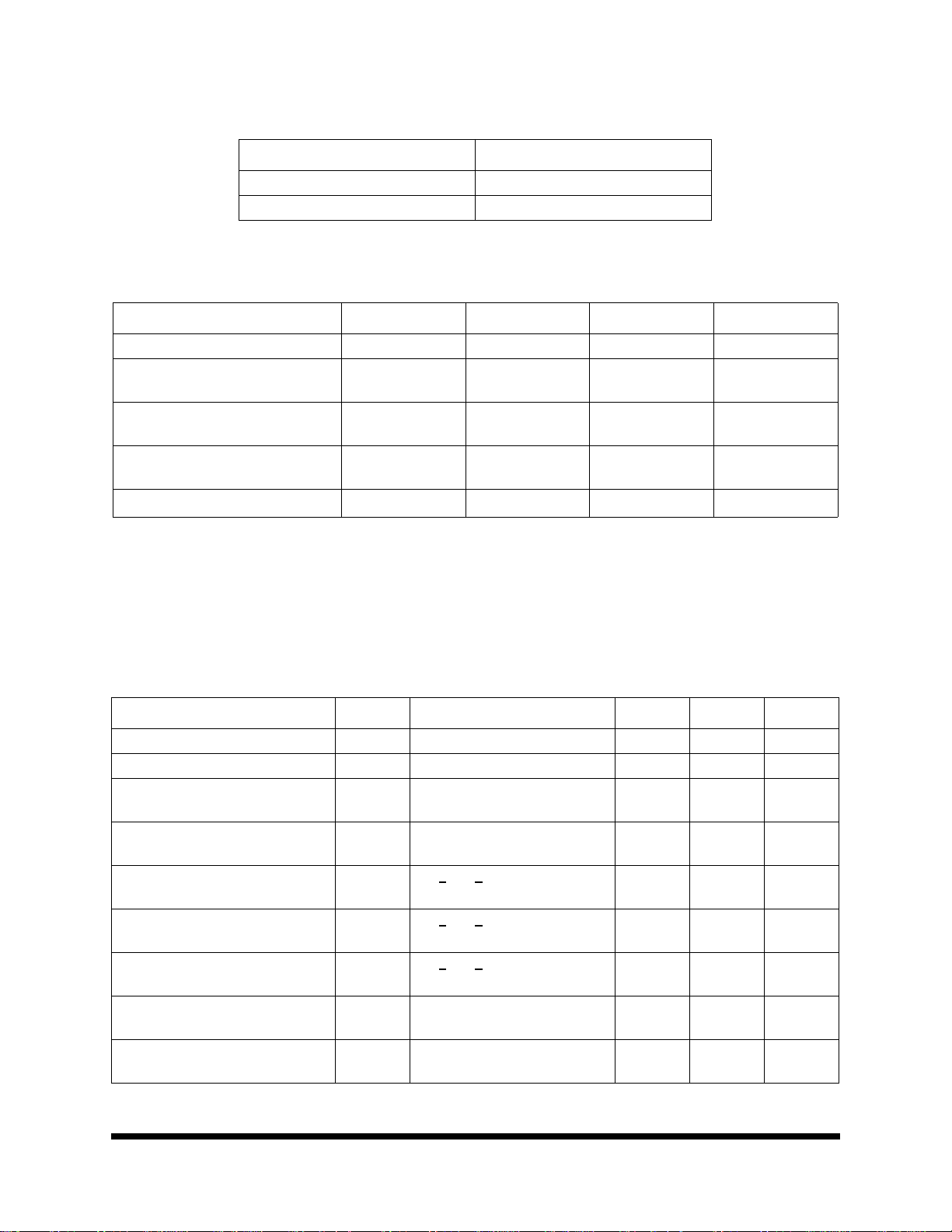
TABLE 1. 7B991 PINOUT DESCRIPTIONS
PIN SYMBOL I/O DESCRIPTION
1 REF I Reference frequency input supplies the frequency and timing
against which all functional variation is measured.
17 FB I PLL feedback (typically connected to one of the eight outputs)
3 FS I Three-level frequency range select. See Table 2.
26, 27 1F0, 1F1 I Three-level function select inputs for output pair 1 (1Q0, 1Q1). See
Table 2.
29, 30 2F0, 2F1 I Three-level function select inputs for output pair 2 (2Q0, 2Q1). See
Table 2.
4, 5 3F0, 3F1 I Three-level function select inputs for output pair 3 (3Q0, 3Q1). See
Table 2.
6, 7 4F0, 4F1 I Three-level function select inputs for output pair 4 (4Q0, 4Q1). See
Table 2.
31 TEST I Three-level select. See test mode section under the block diagram
descriptions.
23, 24 1Q1, 1Q0 O Output pair 1. See Table 2.
21, 22 2Q1, 2Q0 O Output pair 2. See Table 2.
14, 15 3Q1, 3Q0 O Output pair 3. See Table 2.
10, 11 4Q1, 4Q0 O Output pair 4. See Table 2.
9, 16, 18, 25 V
2V
12, 13, 21,
22, 28, 32
CCN
CCQ
GND PWR Ground.
PWR Power supply for output drivers
PWR Power supply for internal circuitry
7B991
Memory
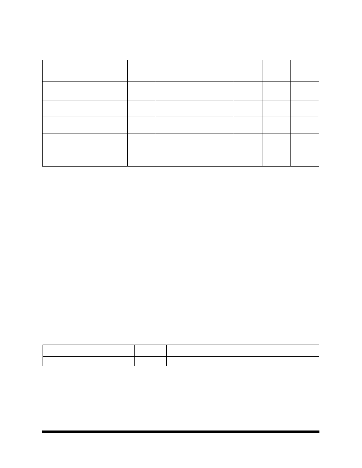
TABLE 2. 7B991 ABSOLUTE MAXIMUM RATINGS
PARAMETER SYMBOL MIN MAX UNIT
Storage Temperature T
Operating Temperature Range T
Supply Voltage to Ground Potential V
DC Input Voltage V
Output Current into Outputs (LOW) I
Static Discharge Voltage (per MIL-STD-882, Method 3015) V
Latchup Current I
1000604
12.19.01 Rev 3
S
A
S
I
OUT
SD
LU
All data sheets are subject to change without notice
-65 150 °C
-40 85 °C
-0.5 7.0 V
-0.5 7.0 V
-- 64 mA
>2001 -- V
>200 -- mA
©2001 Maxwell Technologies.
All rights reserved.
2
Programmable Skew Clock Buffer (PSCB)
TABLE 3. DELTA LIMITS
PARAMETER VARIATION
7B991
I
CCQ
I
CCN
±10% of specified value in Table 5
±10% of specified value in Table 5
TABLE 4. 7B991 RECOMMENDED OPERATING CONDITIONS
PARAMETER SYMBOL MIN MAX UNIT
Supply Voltage V
Input HIGH Voltage (REF and FB
CC
V
IH
inputs only)
Input LOW Voltage (REF and FB
V
IL
inputs only)
Three-Level Input HIGH Voltage (Test,
FS, xFn)
1
Thermal Impedance
Θ
V
IHH
JC
1. These inputs are normally wired to VCC,GND, or left unconnected (actual threshold voltages vary as a percentage of VCC).
Internal termination resistors hold unconnected inputs at V
puts may glitch and the PLL may require an additional t
CC
time before all datasheet limits are achieved.
LOCK
-0.5 +7.0 V
2.0 V
CC
V
-0.5 0.8 V
VCC-0.85 V
CC
V
-- 3.43 °C/W
/2. If these inputs are switched, the function and timing of the out-
Memory
TABLE 5. 7B991 DC ELECTRICAL CHARACTERISTICS
(VCC = 5V ±10%, TA = -40 TO 85°C, UNLESS OTHERWISE SPECIFIED)
P
ARAMETER SYMBOL TEST CONDITIONS MIN MAX UNIT
Output HIGH Voltage V
Output LOW Voltage V
Input HIGH Voltage (REF and FB
inputs only)
Input LOW Voltage (REF and FB
inputs only)
Three-Level Input HIGH Voltage
(Test, FS, xFn)
Three-Level Input MID Voltage (Test,
FS, xFn)
Three-Level Input LOW Voltage (Test,
FS, xFn)
Input HIGH Leakage Current
(REF and FB inputs only)
Input LOW Leakage Current
(REF and FB inputs only)
1
1
1
VCC = Min, IOH = -16 mA 2.4 -- V
OH
VCC = Min, IOL = 46 mA -- 0.45 V
OL
V
IH
V
IL
V
V
V
I
I
Min < VCC < Max VCC-0.85 -- V
IHH
Min < VCC < Max VCC/2 -
IMM
Min < VCC < Max 0.0 0.85 V
ILL
VCC = Max, VIN = 5V -- 10 µA
IH
VCC = Max, VIN = 0.4V -500 -- µA
IL
2.0 -- V
-- 0.8 V
VCC/2 +
500 mV
500 mV
V
1000604
12.19.01 Rev 3
All data sheets are subject to change without notice
©2001 Maxwell Technologies.
All rights reserved.
3
Programmable Skew Clock Buffer (PSCB)
TABLE 5. 7B991 DC ELECTRICAL CHARACTERISTICS
(VCC = 5V ±10%, TA = -40 TO 85°C, UNLESS OTHERWISE SPECIFIED)
P
ARAMETER SYMBOL TEST CONDITIONS MIN MAX UNIT
7B991
Input HIGH Current (Test, FS, xFn) I
Input MID Current (Test, FS, xFn) I
Input LOW Current (Test, FS, xFn) I
Output Short Circuit (Test, FS, xFn)
2
IMM
I
VIN = V
IH
CC
-- 200 µA
VIN = 2.75 -200 200 µA
VIN = GND -- -200 µA
ILL
OS
VCC = Max., V
= GND (25 °C
OUT
-- -250 mA
only)
Operating Current used by Internal
Circuitry
Output Buffer Current per Output Pair
3
Power Dissipation per Output Pair
4
I
CCQ
I
CCN
CCN
= Max, all input
CCQ
selects open
V
= V
CCN
CCQ
= Max, I
= 0 mA,
OUT
Input selects open, fMAX
P
V
= V
D
CCN
CCQ
= Max, I
OUT
= 0 mA
-- 90 mA
-- 14 mA
-- 78 mW
V
= V
Input selects open, fMAX
1. These inputs are normally wired to V
Internal termination resistors hold unconnected inputs at V
puts may glitch and the PLL may require an additional t
,GND, or left unconnected (actual threshold voltages vary as a percentage of VCC).
CC
/2. If these inputs are switched, the function and timing of the out-
CC
time before all datasheet limits are achieved.
LOCK
2. This device should be tested one output at a time, output shorted for less than one second, less than 10% duty cycle. Room
temperature only.
3. Total output current per output pair can be approximated by the following expression that includes device current plus load current:
ICCN = [(4 + 0.11F) + [((835-3F)/Z) + (.0022FC)]N] x 1.1
Where:
f = frequency in MHz
C = capacitive load in pF
Z = line impedance in ohms
N = number of loaded outputs; 0, 1, or 2
FC = F < C
4. Total power dissipation per output pair can be approximated by the following expression that includes device power dissipation
due to the load circuit:
PD = [(22 + 0.61F) + [((1550-2.7F)/Z) + (.0125FC)]N] x 1.1
Memory
TABLE 6. 7B991 CAPACITANCE
P
ARAMETER SYMBOL TEST CONDITIONS MAX UNIT
Input Capacitance C
1. Guaranteed by design.
1000604
1
TA = 25 °C, f = 1 MHz, VCC = 5.0V 10 pF
IN
12.19.01 Rev 3
All data sheets are subject to change without notice
4
©2001 Maxwell Technologies.
All rights reserved.

Programmable Skew Clock Buffer (PSCB)
FIGURE 1. TTL AC TEST LOAD
FIGURE 2. TTL INPUT TEST WAVEFORM
7B991
Memory
TABLE 7. AC ELECTRICAL CHARACTERISTICS
(VCC = 5V ±10%, TA = -40 TO 85°C, UNLESS OTHERWISE SPECIFIED)
P
ARAMETER SYMBOL MIN TYP MAX UNIT
Operating Clock Frequency in MHz FS = LOW
REF Pulse Width HIGH t
REF Pulse Width LOW t
Programmable Skew Unit t
Zero Output Matched-Pair Skew (XQ0, XQ1)
Zero Output Skew (All Outputs)
6,8,9
Output Skew (Rise-Rise, Fall-Fall, Same Class Out-
6,10
puts)
Output Skew (Rise-Fall, Nominal-Inverted, DividedDivided)
6,10
Output Skew (Rise-Rise, Fall-Fall, Different Class
Outputs)
6,10
Output Skew (Rise-Fall, Nominal-Divided, DividedInverted)
Device-to-Device Skew
6,10
1,11,12
Propagation Delay, REF Rise to FB Rise t
Output Duty Cycle Variation
13
1,4
FS = MID
FS = HIGH
1,4,5
6,7
1,4
t
SKEWPR
t
SKEW0
t
SKEW1
t
SKEW2
t
SKEW3
t
SKEW4
t
f
NOM
RPWH
RPWL
U
t
DEV
PD
ODCV
1,2,3
15 -- 30 MHz
25 -- 50
40 -- 80
5.0 -- -- ns
5.0 -- -- ns
See Table 2
-- 0.1 0.50 ns
-- 0.3 0.75 ns
-- 0.6 1.0 ns
-- 1.0 1.5 ns
-- 0.7 1.2 ns
-- 1.2 1.7 ns
-- -- 1.65 ns
-1 0.0 1 ns
-1.2 0.0 1.2 ns
1000604
12.19.01 Rev 3
All data sheets are subject to change without notice
©2001 Maxwell Technologies.
All rights reserved.
5

Programmable Skew Clock Buffer (PSCB)
7B991
TABLE 7. AC ELECTRICAL CHARACTERISTICS
1,2,3
(VCC = 5V ±10%, TA = -40 TO 85°C, UNLESS OTHERWISE SPECIFIED)
P
ARAMETER SYMBOL MIN TYP MAX UNIT
Output HIGH Time Deviation from 50%
Output LOW Time Deviation from 50%
Output Rise Time
Output Fall Time
PLL Lock Time
14,16
14,16
17
Cycle-to-Cycle Output Jitter Peak-to-
1. The level to be set of FS in determined by the “normal” operating frequency (f
Logic Block Diagram). Nominal frequency (f
undivided modes (See Table 9). The frequency appearing at the REF and FB inputs will be f
FB is undivided. The frequency of the REF and FB inputs will be f
14,15
14,15
t
PWH
t
PWL
t
ORISE
t
OFALL
t
LOCK
t
3
Peak
) always appears at 1Q0 and the other outputs when they are operated in their
NOM
JR
-- -- 3 ns
-- -- 3.5 ns
0.15 1.5 2.5 ns
0.15 1.5 2.5 ns
-- -- 0.5 ms
-- -- 200 ps
) of the VCO and Time Unit Generator (see
NOM
when the output connected to
NOM
NOM
/2 or f
/4 when the part is configured for a frequency
NOM
multiplication by using a divided output as the FB input.
2. Test measurement levels for the 7B991 are TTL levels (1.5V to 1.5V). Test conditions assume signal transition times of 2 ns or
less and output loading as shown in the AC Test Loads and Waveforms unless otherwise specified.
3. Guaranteed by statistical correlation. Tested initially and after any design or process changes that may affect these parameters.
4. For all three state inputs. HIGH indicates a connection to V
connections. Internal termination circuitry holds an unconnected input to V
5. When the FS pin is selected HIGH, the REF input must not transition upon power-up until V
6. SKEW is defined as the time between the earliest and the latest output transition among all outputs for which the same t
has been selected when all are loaded with 50 pF and terminated with 50
7. t
8. t
is defined as the skew between a pair of outputs (XQ0 and XQ1) when all eight outputs are selected for 0tU.
SKEWPR
is defined as the skew between outputs when they are selected for 0tU. Other outputs are divided or inverted but not
SKEW0
, LOW indicates a connection to GND, and MID indicates an open
CC
CC
/2.
has reached 4.3V.
CC
U
Ω to 2.06V.
delay
shifted.
9. C
= 0 pF. For CL = 30 pF, t
L
10.There are three classes of outputs: Nominal (multiple of t
SKEW0
= 0.35 ns.
delay), Inverted (4Q0 and 4Q1 only with 4F0 = 4F1 = HIGH), and
U
divided (3Qx and 4Qx only in Divide-by-2 or Divide-by-4 mode).
11. t
is the output-to-output skew between any two devices operating under the same conditions (VCC ambient temperature, air
DEV
flow, etc.)
12.Guaranteed by design.
13.t
is the deviation of the output from a 50% duty cycle. Output pulse width variations are included in t
ODCV
SKEW2
and t
SKEW4
spec-
ifications.
14.Specified with outputs loaded 30 pF for the 7B99 devices. Devices are terminated through 50
15.t
is measured at 2.0V. t
PWH
16.t
17.t
and t
ORISE
is the time that is required before synchronization is achieved. This specification is valid only after VCC is stable and within
LOCK
measured between 0.8V and 2.0V.
OFALL
is measured at 0.8V.
PWL
normal operating limits. This parameter is measured from the application of a new signal or frequency at REF or FB until t
Ω to 2.05V.
is
PD
within specified limits.
Memory
1000604
12.19.01 Rev 3
All data sheets are subject to change without notice
©2001 Maxwell Technologies.
All rights reserved.
6
 Loading...