

MAXWELL 7545ARPDS, 7545ARPDI, 7545ARPDE, 7545ARPDB Datasheet
M
e
m
ory
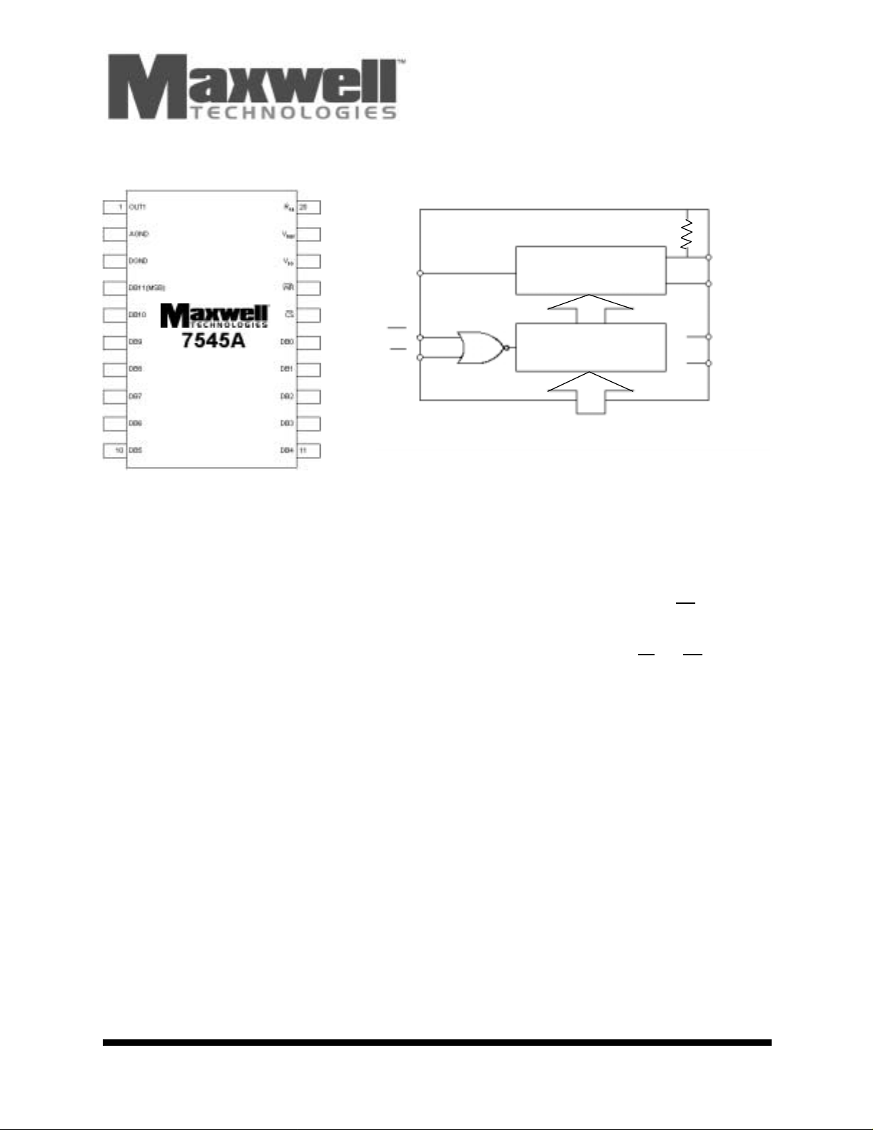
7545A
12-Bit Buffered Multiplying
Digital to Analog Converter
R
FB
R
V
REF
12-BIT MULTIPYING
DAC
12
OUT1
AGND
WR
CS
FEATURES:
•RAD-PAK® patented shielding against natural space radia-
tion
• Total dose hardness:
- > 100 krad (Si), depending upon space mission
• Excellent single event effects
- SEL
: > 120 MeV/mg/cm
TH
- SEUTH: > 120 MeV/mg/cm2 using all 1’s
• Package:
- 20 pin R
- 20 pin R
• Low gain temperature coefficient:
- 5 ppm/
• Fast interface timing
• Single +5 V to +15 V supply
AD-PAK® Flat Pack
AD-PAK® DIP
°
C typ.
2
V
INPUT D A TA LATCH E S
12
DB11-DBO
DD
DGND
DESCRIPTION:
Maxwell Technologies’ 7545A is a 12-bit CMOS-buffered multiplying DAC with internal data latches, which features a
greater than 100 krad (Si) total dose tolerance, depending
upon space mission. The 7545A features a WR
100 ns which allows interfacing to a much wider range of fast
8-bit and 16-bit microprocessors. It is loaded by a single 12-bit
wide word under the control of the CS
these control inputs low makes the input latches transparent
allowing unbuffered operation of the DAC. The 7545A is particularly suitable for single supply operations and applications
with wide temperature variations.
Maxwell Technologies' patented R
ogy incorporates radiation shielding in the microcircuit package. It eliminates the need for box shielding while providing
the required radiation shielding for a lifetime in orbit or space
mission. In a GEO orbit, R
krad (Si) radiation dose tolerance. This product is available
with screening up to Class S.
AD-PAK® packaging technol-
AD-PAK provides greater than 100
pulse width of
and WR inputs; tying
(858) 503-3300- Fax: (858) 503-3301- www.maxwell.com
02.05.02 REV 4
All data sheets are subject to change without notice
©2001 Maxwell Technologies
All rights reserved.
1
M
e
m
ory
12-Bit Buffered Multiplying
Digital to Ana log Converter
TABLE 1. 7545A PINOUT DESCRIPTION
PIN SYMBOL DESCRIPTION
1 OUT 1 Output Current
2 AGND Analog Ground
3 DGND Digital Ground
4 DB 11 Data Bit 11 (MSB)
5 DB 10 Data Bit 10
6 DB 9 Data Bit 9
7 DB 8 Data Bit 8
8 DB 7 Data Bit 7
9 DB 6 Data Bit 6
10 DB 5 Data Bit 5
11 DB 4 Data Bit 4
12 DB 3 Data Bit 3
13 DB 2 Data Bit 2
14 DB 1 Data Bit 1
15 DB 0 Data Bit 0 (LSB)
16 CS
17 WR
18 V
19 V
20 RFB Feedback Resistance
DD
REF
7545A
Chip Select (Active Low)
Write (Active Low)
Digital Supply Voltage
Reference Input
TABLE 2. 7545A ABSOLUTE MAXIMUM RATINGS
PARAMETER SYMBOL MIN MAX UNIT
VDD to DGND -- -0.3 17 V
Digital Input Voltage to DGND -- -0.3 V
, V
V
RFB
V
PIN1
AGND to DGND -- -0.3 V
Power Dissipation to 75
Thermal Impedance — Flat Package
Thermal Impedance — DIP Package
Operating Temperature -- -55 125
Storage Temperature Range T
to DGND -- -- 25 V
REF
to DGND -- -0.3 VDD + 0.3 V
°
CP
02.05.02 REV 4
Θ
Θ
D
JC
JC
S
-- 450 mW
-- 6.08 °C/W
-- 6.04 °C/W
-65 150
+ 0.3 V
DD
+ 0.3 V
DD
°
C
°
C
©2001 Maxwell Technologies
All rights reserved.
2All data sheets are subject to change without notice
M
e
m
ory
12-Bit Buffered Multiplying
Digital to Analog Converter
TABLE 3. DELTA LIMITS
PARAMETER VARIATION
7545A
I
DD
± 10%
TABLE 4. 754 5A SP ECIFICA TIO NS
(VDD = +5 V, TA = -55 TO 125 °C UNLESS OTHERWISE NOTED)
EST SYMBOL TEST CONDITION MIN MAX UNIT
T
Resolution RES 12 -- Bits
Relative Accuracy RA -1/ 2 1/2 LSB
Differential Nonlinearity DNL 12-Bit Monotonic T
Gain Error
1
A
DAC Register Loaded with
E
MIN
to T
MAX
1111 1111 11 11
Gain Temperature Coefficient
2
Power Supply Rejection PSRR ∆V
Output Current Settling Time
2
TC
AE
DD = +/- 5% -0.004 0.004 %/%
t
SL
To 1/2LSB; OUT1 Load = 100Ω,
DAC Output Measured from
Falling Edge of WR
. CS = 0V
Feed through Error FT 5 (typical) mV p-p
Reference Input Resistance
(Pin 19 to Ground)
2
R
IN
-1 1 LSB
-4 4 LSB
-5 5 ppm/°C
-- 1 µs
10 20 KΩ
Digital Input High Voltage V
Digital Input Low Voltage V
Digital Input Leakage Current I
Digital Input Capacitance
Output Capacitance
Chip Select to Write Setup Time
Chip Select to Write Hold Time
Write Pulse Width
Data Setup Time
Data Hold Time
3
Supply Current from V
2
2
3
3
3
3
DD
1. Measured using feedback resistor.
2. Guaranteed by design.
C
IN
C
OUT1
t
CS
t
CH
t
WR
t
DS
t
DH
I
DD
IH
IL
VIN = 0 V or V
DB0 - DB11; WR, CS -- 15 pF
IN
DD
2.4 -- V
-- 0.8 V
-10 10 µA
DB0 - DB11 = 0 V, WR, CS = 0V -- 70 pF
DB0 - DB11 = V
, WR, CS = 0V -- 150
DD
tCS > tWR, tCH > 0 170 -- nS
0-170 -150 --
5--
All Digital Inputs VIL or V
All Digital Inputs 0 or V
DD
IH
2
-- 2 mA
-- 100 µA
02.05.02 REV 4
3All data sheets are subject to change without notice
©2001 Maxwell Technologies
All rights reserved.
 Loading...