MAXWELL 7025ERPQS45, 7025ERPQS35, 7025ERPQI45, 7025ERPQI35, 7025ERPQE45 Datasheet
...
1
Memory
All data sheets are subject to change without notice
(619) 503-3300- Fax: (619) 503-3301- www.maxwell.com
(8K x 16-Bit) Dual Port RAM
7025E
©2001 Maxwell Technologies
All rights reserved.
High-Speed CMOS
12.19.01 Rev 2
1000586
FEATURES:
• 8K x 16-bit dual port RAM
- Stand Alone
- Master Slave
•R
AD-PAK® radiation-hardened against natural space
radiation
• Total dose hardness:
- > 100 krad (Si), depending upon space mission
• Excellent Single Event Effects:
-SEL
TH
LET = >100 MeV/mg/cm
2
-SEUTH LET = 7 MeV/mg/cm
2
• Package:
-84 Pin R
AD-PAK® quad flat pack
• Separate upper byte and lower byte control for multiplexed
bus compatibility
• High speed access time: 35/45 ns
• Expandable to 32 bits or more using master/slave select
when cascading
• High speed CMOS technology
-TTL compatible, single 5V power supply
-Interrupt flag for port-to-port communication
-On chip port arbitration logic
-Asynchronous operation from either port
DESCRIPTION:
Maxwell Technologies’ 7025E Dual Port RAM High Speed
CMOS® microcircuit features a greater than 100 krad (Si) total
dose tolerance, depending upon space mission. The 7025E is
designed to be used as a stand-alone 128k-bit Dual Port RAM
or as a combination MASTER/SLAVE Dual-Port RAM for 32bit or more word systems. This design results in full-speed,
error-free operation without the need for additional discrete
logic. The 7025E provides two independent ports with separate control, address, and I/O pins that permit independent,
asynchronous access for reads or writes to any location in
memory. An automatic power down feature controlled by CS
permits the on-chip circuitry of each port to enter a very low
standby power mode.
Maxwell Technologies' patented R
AD-PAK® packaging technol-
ogy incorporates radiation shielding in the microcircuit package. It eliminates the need for box shielding while providing
the required radiation shielding for a lifetime in orbit or space
mission. In a GEO orbit, R
AD-PAK provides greater than 100
krad (Si) radiation dose tolerance. This product is available
with screening up to Class S.
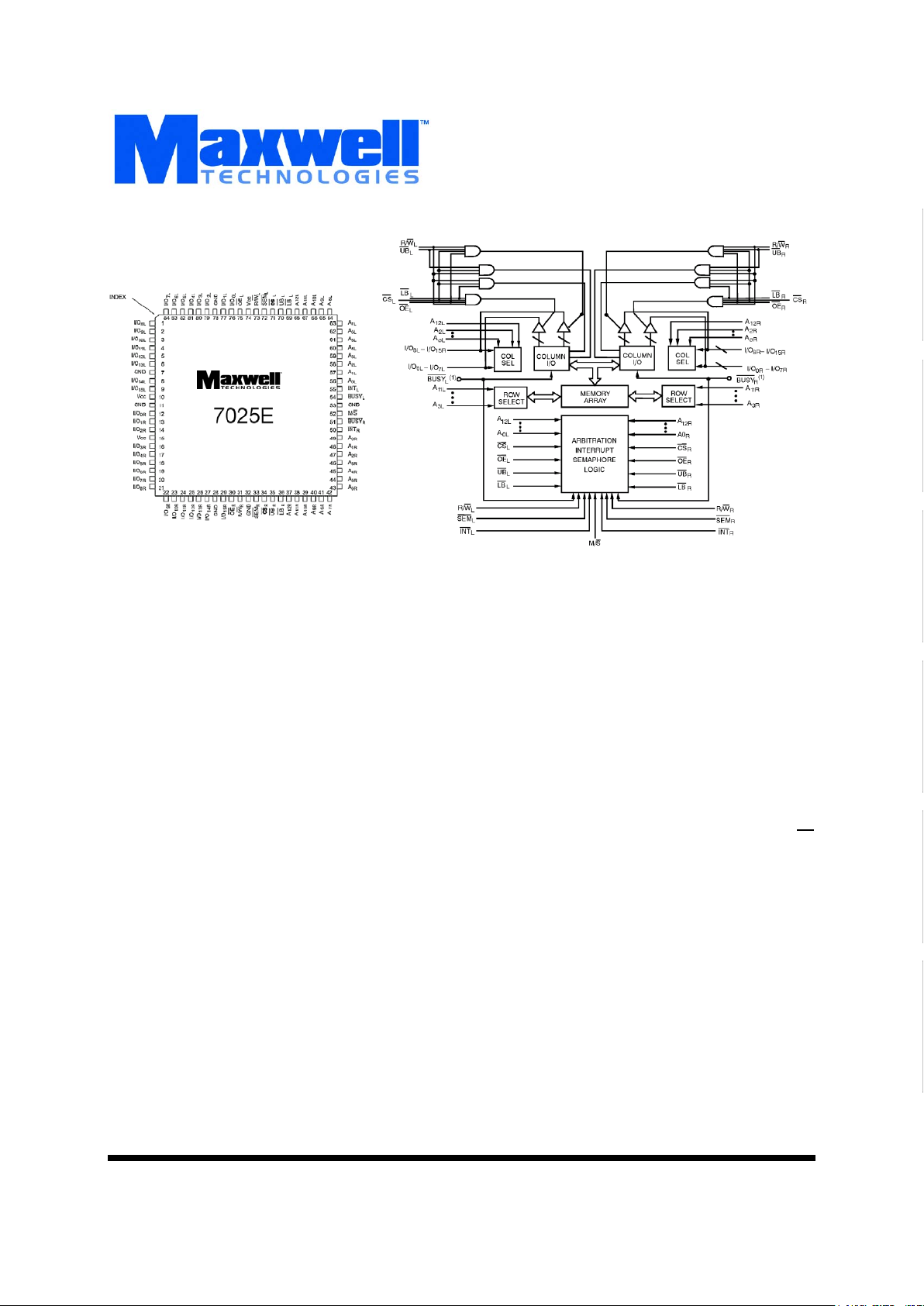
Logic Diagram

Memory
2
All data sheets are subject to change without notice
©2001 Maxwell Technologies
All rights reserved.
(8K x 16-Bit) Dual Port RAM High-Speed CMOS
7025E
12.19.01 Rev 2
1000586
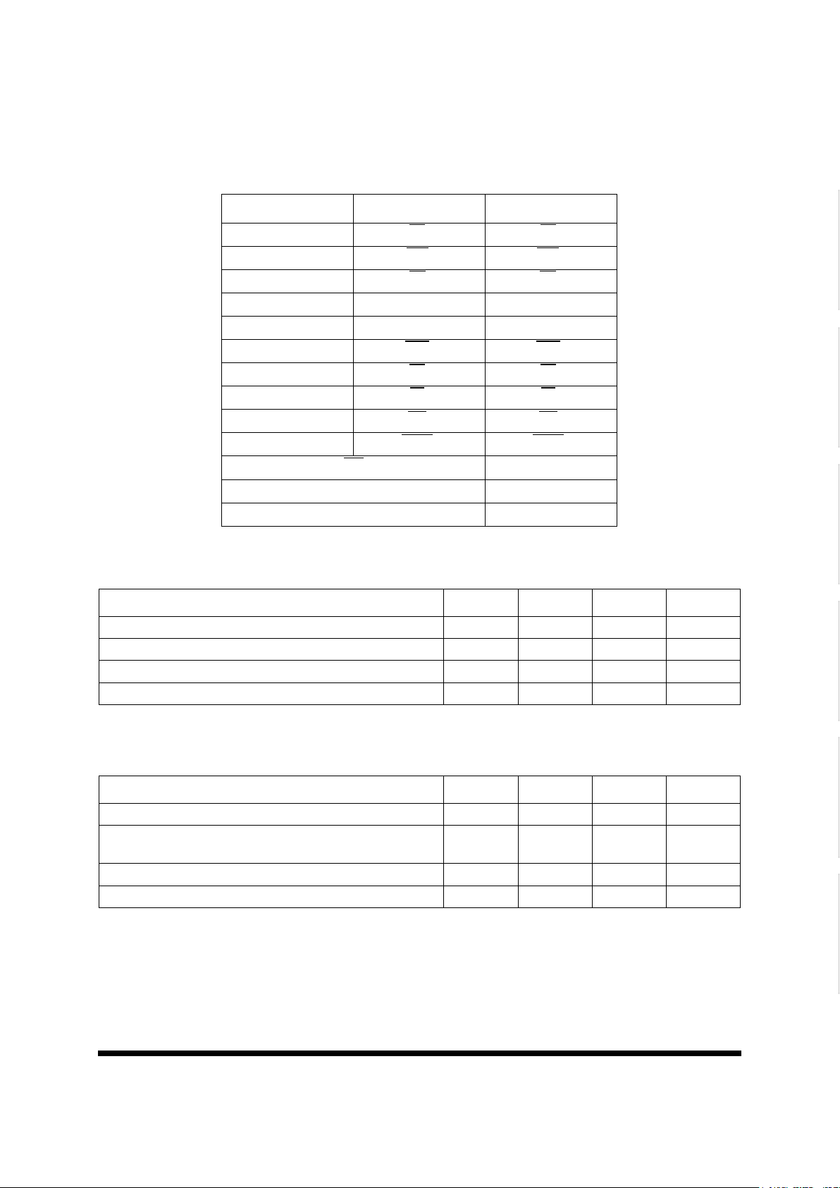
TABLE 1. 7025E PINOUT DESCRIPTION
NAMES LEFT PORT RIGHT PORT
Chip Select CS
L
CS
R
Read/Write Select R/W
L
R/W
R
Output Select OS
L
OS
R
Address AOL-A12
L
AOR-A12
R
Data Input/Output I/OOL-I/O15
L
I/OOR-I/O15
R
Semaphore Select SEM
L
SEM
R
Upper Byte Select UB
L
UB
R
Lower Byte Select LB
L
LB
R
Interrupt Flag INT
L
INT
R
Busy Flag BUSY
L
BUSY
R
M/S Master or Slave Select
V
CC
Power
GND Ground
TABLE 2. 7025E ABSOLUTE MAXIMUM RATINGS
PARAMETER SYMBOL MIN MAX UNITS
Supply Voltage (Relative to VSS)V
CC
-0.3 7.0 V
Operating Temperature Range T
A
-55 125
°
C
Input or Output Voltage Applied -- GND -0.3V V
CC
+ 0.3 V
Storage Temperature Range T
STG
-65 150
°
C
TABLE 3. 7025E RECOMMENDED OPERATING CONDITIONS
PARAMETER SYMBOL MIN MAX UNITS
Supply Voltage Positive V
CC
4.5 5.5 V
Input Voltage V
IL
V
IH
-0.5
2.2
0.8
6.0
V
Thermal Impedance
Θ
JC
-- 1.02 °C/W
Operating Temperature Range T
A
-55 125
°
C

Memory
3
All data sheets are subject to change without notice
©2001 Maxwell Technologies
All rights reserved.
(8K x 16-Bit) Dual Port RAM High-Speed CMOS
7025E
12.19.01 Rev 2
1000586
TABLE 4. 7025E CAPACITANCE
PARAMETER SYMBOL MIN MAX UNITS
Input Capacitance: VIN = 0V
1
1. Guaranteed by design.
C
IN
-- 5 pF
Output Capacitance: V
OUT
= 0V
1
C
OUT
-- 7 pF
TABLE 5. 7025E DC ELECTRICAL CHARACTERISTICS
(VCC = 5V ± 10%, TA = -55 TO 125 °C UNLESS OTHERWISE)
P
ARAMETER SYMBOL MIN MAX UNITS
Input Leakage Current
1
1. VCC = 5.5V, VIN = GND to VCC, CS = VIH, VOUT = 0 to VCC.
I
LI
-- ±10 µA
Output Leakage Current
2
2. VIH max = VCC + 0.3V, VIL min = -0.3V or -1V pulse width 50 ns.
I
LO
-- ±10 µA
Standby Supply Current, Both ports TTL level inputs
-35
-45
I
CCSB
--
--
50
50
mA
Standby Supply Current, Both ports CMOS level inputs
-35
-45
I
CCSB1
--
--
5000
5000
µA
Operating Supply Current, Both ports Active
-35
-45
I
CCOP
--
--
320
280
mA
Operating Supply Current, One Port Active, One Port Standby
-35
-45
I
CCOP1
--
--
190
180
mA
Input Low Voltage
Input High Voltage
V
IL
V
IH
--
2.2
0.8
--
V
Output Low Voltage
3
Output High Voltage
3. V
CC
min, IOL = 4 mA, IOH = -4 mA.
V
OL
V
OH
--
2.4
0.4
--
V
TABLE 6. 7025E AC ELECTRICAL CHARACTERISTICS FOR READ CYCLE
(VCC = 5V ± 10%, VSS = 0V, TA = -55 TO 125 °C)
P
ARAMETER SYMBOL MIN MAX UNIT
Read Cycle Time
-35
-45
t
RC
35
45
--
--
ns

Memory
4
All data sheets are subject to change without notice
©2001 Maxwell Technologies
All rights reserved.
(8K x 16-Bit) Dual Port RAM High-Speed CMOS
7025E
12.19.01 Rev 2
1000586
Address Access Time
-35
-45
t
AA
--
--
35
45
ns
Chip Select Access Time
1
-35
-45
t
ACS
--
--
35
45
ns
Byte Select Access Time
1
-35
-45
t
ABE
--
--
35
45
ns
Output Select to Output Valid
-35
-45
t
AOE
--
--
20
25
ns
Output Low Z Time
2,3
-35
-45
t
LZ
3
3
--
--
ns
Output High Z Time
2,3
-35
-45
t
HZ
--
--
20
20
ns
Chip Enable to Power Up Time
2
t
PU
0--ns
Chip Disable to Power Up Time
2
t
PD
-- 50 ns
Semaphore Flag Update Pulse (OE
or SEM)t
SOP
15 -- ns
1. To access RAM, CS
= VIL, UB or LB = VIL, SEM = VIH. To access semaphore, CS = VIN and SEM = VIL. Either condition must
be valid for the entire t
EW
time.
2. Guaranteed by design.
3. Transition is measured ± 500 mV from low or high impedance voltage with load.
TABLE 7. 7025E AC ELECTRICAL CHARACTERISTICS FOR WRITE CYCLE
(VCC = 5V ± 10%, VSS = 0V, TA = -55 TO 125 °C)
P
ARAMETER SYMBOL MIN MAX UNIT
Write Cycle Time
-35
-45
t
WC
35
45
--
--
ns
Address Valid to End of Write
-35
-45
t
AW
30
40
--
--
ns
Chip Select to End of Write
1
-35
-45
t
SW
30
40
--
--
ns
TABLE 6. 7025E AC ELECTRICAL CHARACTERISTICS FOR READ CYCLE
(VCC = 5V ± 10%, VSS = 0V, TA = -55 TO 125 °C)
P
ARAMETER SYMBOL MIN MAX UNIT

Memory
5
All data sheets are subject to change without notice
©2001 Maxwell Technologies
All rights reserved.
(8K x 16-Bit) Dual Port RAM High-Speed CMOS
7025E
12.19.01 Rev 2
1000586
Address Setup Time
-35
-45
t
AS
0
0
--
--
ns
Write Pulse Width
-35
-45
t
WP
30
35
--
--
ns
Write Recovery Time
-35
-45
t
WR
0
0
--
--
ns
Data Valid to End of Write
-35
-45
t
DW
25
25
--
--
ns
Output High Z Time
2,3
-35
-45
t
HZ
--
--
20
20
ns
Data Hold Time
-35
-45
t
DH
0
0
--
--
ns
Write Select to Output in High Z
2,3
-35
-45
t
WZ
--
--
20
20
ns
Output Active from End of Write
2,3,4
-35
-45
t
OW
0
0
--
--
ns
SEM Flag Write to Read Time
-35
-45
t
SWRD
10
10
--
--
ns
SEM Flag Contention Window
-35
-45
t
SPS
10
10
--
--
ns
1. To access RAM, CS
= VIL, UB or LB = VIL, SEM = VIH. To access semaphore, CS = VIN and SEM = VIL. Either condition must
be valid for the entire t
EW
time.
2. Guaranteed by design.
3. Transition is measured ± 500 mV from low or high impedance voltage with load.
4. The specification for t
DH
must be met by the device supplying write data to the RAM under all operating conditions. Although
t
DH
and tDW.
TABLE 7. 7025E AC ELECTRICAL CHARACTERISTICS FOR WRITE CYCLE
(VCC = 5V ± 10%, VSS = 0V, TA = -55 TO 125 °C)
P
ARAMETER SYMBOL MIN MAX UNIT

Memory
6
All data sheets are subject to change without notice
©2001 Maxwell Technologies
All rights reserved.
(8K x 16-Bit) Dual Port RAM High-Speed CMOS
7025E
12.19.01 Rev 2
1000586
TABLE 8. 7025E AC ELECTRICAL CHARACTERISTICS FOR WRITE MASTER/SLAVE CONFIGURATION
(VCC = 5V ± 10%, VSS = 0V, TA = -55 TO 125 °C)
P
ARAMETER SYMBOL MIN MAX UNIT
For Master Only
BUSY Access Time to Address Match
-35
-45
t
BAA
--
--
35
35
ns
BUSY Disable Time to Address Not Matched
-35
-45
t
BDA
--
--
30
30
ns
BUSY Access Time to Chip Select Low
-35
-45
t
BAC
--
--
30
30
ns
BUSY Disable Time to Chip Select High
-35
-45
t
BDC
--
--
25
25
ns
Write Pulse to Data Delay
1
-35
-45
1. Port to port timing delay through RAM cells from writing port to reading port.
t
WDD
--
--
60
70
ns
Write Data Valid to Read Data Delay
1
-35
-45
t
DDD
--
--
45
55
ns
Arbitration Priority Setup Time
2
-35
-45
2. To ensure that the earlier of the two ports wins.
t
APS
5
5
--
--
ns
BUSY Disable to Valid Data
-35
-45
t
BDD
--
--
3
3
3. t
BDD
is a calculated parameter and is the greater of 0, t
WDD
- tWP (actual) or t
DDD
- tWD (actual).
ns
For Slave Only
Write to BUSY Input
4
4. To ensure that the write cycle is inhibited during contention.
t
WB
0--ns
Write Hold after BUSY
5
5. To ensure that a write cycle is completed after contention.
t
WH
25 -- ns
Write Pulse to Data Delay
1
-35
-45
t
WDD
--
--
60
70
ns
Write Data Valid to Read Data Delay
1
-35
-45
t
DDD
--
--
45
55
ns
 Loading...