查询54LVTH244ARPFB供应商
PRELIMINARY
54LVTH244A
3.3V ABT 8-Bit Octal
Buffers/Drivers
FEATURES:
• 3.3V ABT octal buffers/drivers with 3-state outputs
•R
AD-PAK® radiation-hardened against natural space radia-
tion
• Package:
- 20 Pin R
• Operating temperature range:
-55 to 125
• Supports mixed-mode signal operation
-5V Input and Output Voltages with 3.3V V
• Supports mixed-mode signal operation
- 5V input and output voltages with 3.3V V
• Supports unregulated battery operation down to 2.7V
•Typical V
T
A
• Supports live insertion
• Bus-hold data inputs eliminate the need for external pullup
resistors
AD-PAK® flat package
°
C
(output ground bounce) < 0.8V at VCC=3.3V,
OLP
=25°C
CC
CC
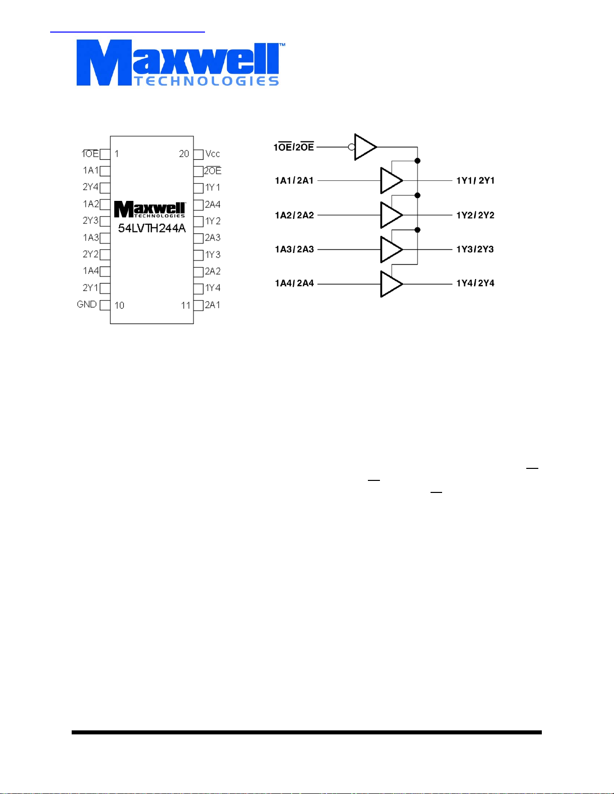
Logic Diagram
DESCRIPTION:
Maxwell Technologies’ 54LVTH244A octal buffers/drivers
micro-circuit is housed in a Rad-Pak® package. The
54LVTH244A is designed specifically for low voltage (3.3V)
V
operation, but with the capability to provide a TTL inter-
CC
face to a 5V system environment. The 54LVTH244A is organized as two 4-bit drivers with separate output enable (OE
inputs. When OE
inputs to the Y outputs. When OE
the high impedance state. The 54LVTH244A active bus hold
circuitry is provided to prevent floating data inputs at a valid
logic level and to eliminate the need for pullup resistors.
Maxwell Technologies' patented R
ogy incorporates radiation shielding in the microcircuit package. It eliminates the need for box shielding while providing
the required radiation shielding for a lifetime in orbit or a space
mission. This product is available with packaging and screening up to Class S.
is low, the device passes data from the A
is high, the outputs are in
AD-PAK® packaging technol-
Memory
)
1000601
(858) 503-3300 - Fax: (858) 503-3301 - www.maxwell.com
12.19.01 Rev 1
All data sheets are subject to change without notice
©2001 Maxwell Technologies
All rights reserved.
1

3.3V ABT 8-Bit Octal Buffers/Drivers
TABLE 1. PINOUT DESCRIPTION
PRELIMINARY
PIN SYMBOL DESCRIPTION
1, 19 1OE-2OE Output Enable
2, 4, 6, 8 IA1-IA4 Input
3, 5, 7, 9 2Y4-2Y1 Output
10 GND Ground
11, 13, 15, 17 2A1-2A4 Input
12, 14, 16, 18 1Y4-1Y1 Output
54LVTH244A
20 V
CC
TABLE 2. 54LVTH244A ABSOLUTE MAXIMUM RATINGS
P
ARAMETER SYMBOL MIN MAX UNIT
Supply Voltage Range V
Input Voltage Range
Voltage Range Applied to Any Output in the High State or Power-Off
2
Supply Voltage
CC
V
I
V
O
1
-0.5 4.6 V
-0.5 7.0 V
-0.5 7.0 V
State
Current into Any Output in the Low State I
Current Into Any Output in the High State
Input Clamp Current (V
Output Clamp Current (V
Total Power Dissipation at T
< 0) I
I
< 0) I
O
= 55 °CP
A
3
Operating Temperature T
Storage Temperature Range T
I
OK
O
O
IK
D
A
S
-- 96 mA
-- 48 mA
-- -50 mA
-- -50 mA
-- 650
mW
-55 125 °C
-65 150
°
C
1. Stresses beyond those listed under “Absolute Maximum Ratings” may cause permanent damage to the device. These are
stress ratings only, and functional operation of the device at these or any other conditions betond those indicated under “Recommended Operating Conditions” is not imp[lied. Exposure to absolute-maximum-rated conditions for extended periods may
affect device reliability.
Memory
2. The input and output negative-voltage ratings may be exceeded if the input and output clamp-current ratings are observed.
3. This current flows only when the output is in the high state and VO > VCC.
1000601
12.19.01 Rev 1
All data sheets are subject to change without notice
©2001 Maxwell Technologies
All rights reserved.
2

3.3V ABT 8-Bit Octal Buffers/Drivers
TABLE 3. DELTA LIMITS
54LVTH244A
PRELIMINARY
TABLE 4. 54LVTH244A RECOMMENDED OPERATING CONDITIONS
ARAMETER SYMBOL MIN MAX UNIT
P
Supply Voltage V
High-level Input Voltage V
Low-level Input Voltage V
Input Voltage V
High-level Output Current I
Low-level Output Current I
Input Transition Rise or Fall Rate
Operating Temperature T
PARAMETER VARIATION
I
CC(OL)
I
OZH
I
OZL
±10% of specified value on Table 5
±10% of specified value on Table 5
±10% of specified value on Table 5
CC
IH
IL
I
OH
OL
∆t/∆v-- 10 ns/V
A
1
2.7 3.6 V
2.0 -- V
-- 0.8 V
-- 5.5 V
-- -24 mA
-- 48 mA
-55 125
1. All unused control inputs must be held high or low toensure proper device operation.
Memory
°
C
TABLE 5. 54LVTH244A DC ELECTRICAL CHARACTERISTICS
(VCC = 3.3V ±10%, TA = -55 °C TO 125 °C, UNLESS OTHERWISE SPECIFIED)
P
ARAMETER SYMBOL TEST CONDITIONS MIN MAX UNIT
Input Clamp Voltage V
High-Level Output Voltage V
Low-Level Output Voltage V
1000601
VCC = 2.7 II = -18mA -- -1.2 V
IK
OHVCC
OL
= 2.7V to 3.6V IOH = -100µA VCC -0.2 -- V
V
= 2.7V IOH = -8mA 2.4 --
CC
V
= 3V IOH = 24mA 2.0 --
CC
VCC = 2.7V IOL = 100µA -- 0.2 V
I
= 24mA -- 0.5
OL
V
= 3V IOL = 16mA -- 0.4
CC
I
= 32mA -- 0.5
OL
I
= 32mA -- 0.55
OL
12.19.01 Rev 1
All data sheets are subject to change without notice
3
©2001 Maxwell Technologies
All rights reserved.
 Loading...