MAXWELL 54HC4049RPFS, 54HC4049RPFI, 54HC4049RPFE, 54HC4049RPFB Datasheet

1
Memory
All data sheets are subject to change without notice
(858) 503-3300 - Fax: (858) 503-3301 - www.maxwell.com
CMOS Logic Hex
54HC4049
©2001 Maxwell Technologies.
All rights reserved.
Inverting Buffers
12.20.01 Rev1
1000589
54HC4049
FEATURES:
• High speed CMOS logic hex inverting Buffers
•R
AD-PAK® radiation hardened against natural space radia-
tion
• Single Event Effects:
- SEL: > 120 MeV/mg/cm2
• Total dose hardness:
• - > 100 Krad (Si), depending upon space mission
• Package:
-16 Pin R
AD-PAK® Flat Pack
• Typical propagation delay:
- 6ns at V
CC
= 5V, CL = 15pF, TA = 25°C
• High-to-Low voltage level converter for up to V
I
= 16V
• Fanout (over temperature range)
-10 LSTTL loads (Standard Outputs)
-15 LSTTL loads (Bus Driver Outputs)
• Balanced propagation delay and transition times
• Significant power reduction compared to LSTTL logic ICs
• 2V to 6V operation
• High noise immunity
•-N
IL
= 30%, NIH = 30% of VCC at VCC = 5V
DESCRIPTION:
Maxwell Technologies' 54HC4049 high speed CMOS Logic
Hex Inverting Buffers features a greater than 100 krad(Si) total
dose tolerance, depending upon space misssion. These parts
have a modified input protection structure that enables them
to be used as logic level translators which will convert highlevel logic to a low-level logic while operating off the low-level
logic supply. For example, 15V input pulse levels can be
down-converted to 0V to 5V logic levels. The modified input
protection structure protects the input from negative electrostatic discharge. The 54HC4049 can be used as simple buffers or inverters without level translation.
Maxwell Technologies' patented R
AD-PAK® packaging technol-
ogy incorporates radiation shielding in the microcircuit package. It eliminates the need for box shielding while providing
the required radiation shielding for a lifetime in orbit or space
mission. In a GEO orbit, R
AD-PAK provides greater than 100
krad (Si) radiation dose tolerance. This product is available
with screening up to Class S.
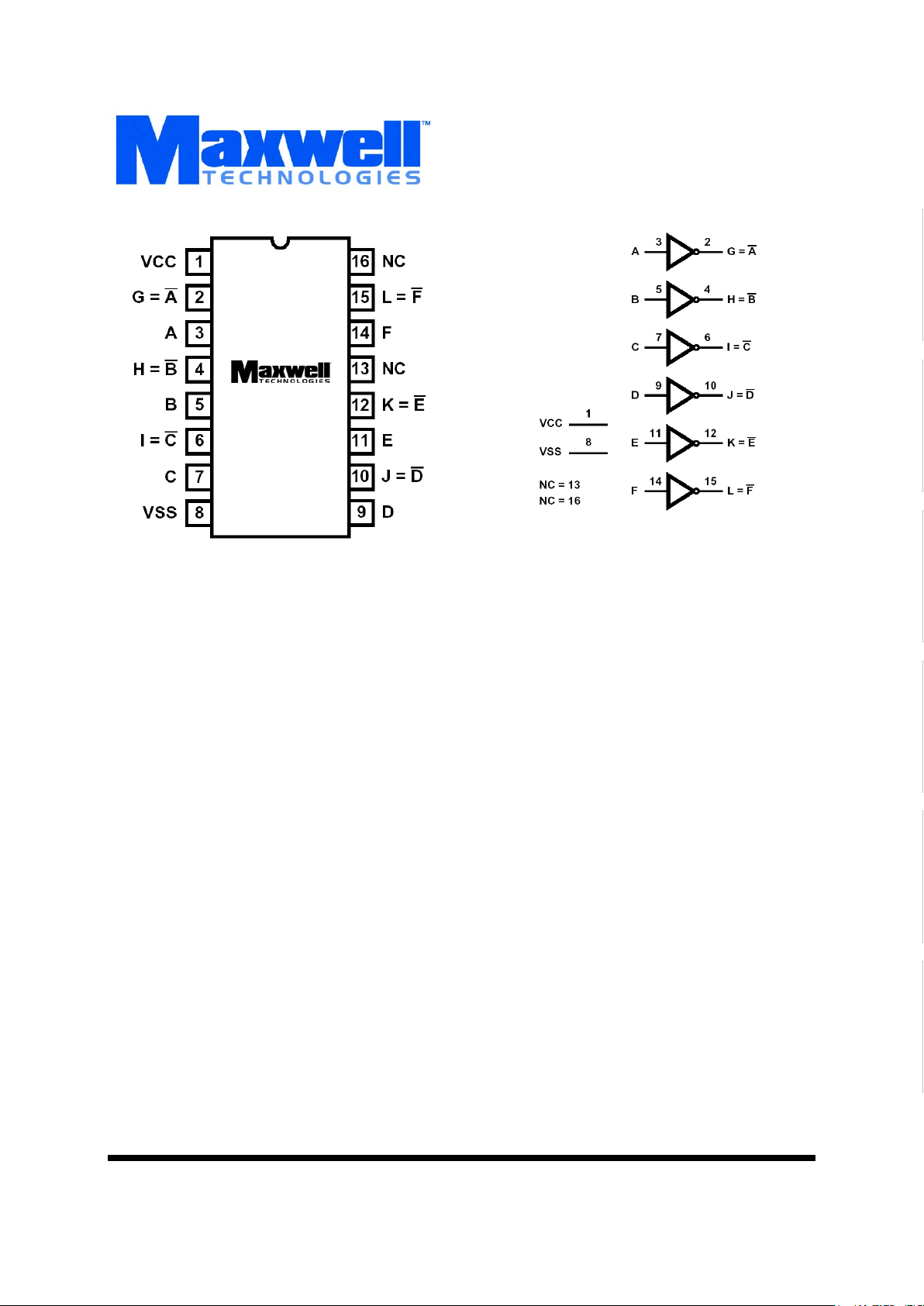
Logic Diagram

Memory
2
All data sheets are subject to change without notice
©2001 Maxwell Technologies.
All rights reserved.
CMOS Logic Hex Inverting Buffers
54HC4049
12.20.01 Rev1
1000589
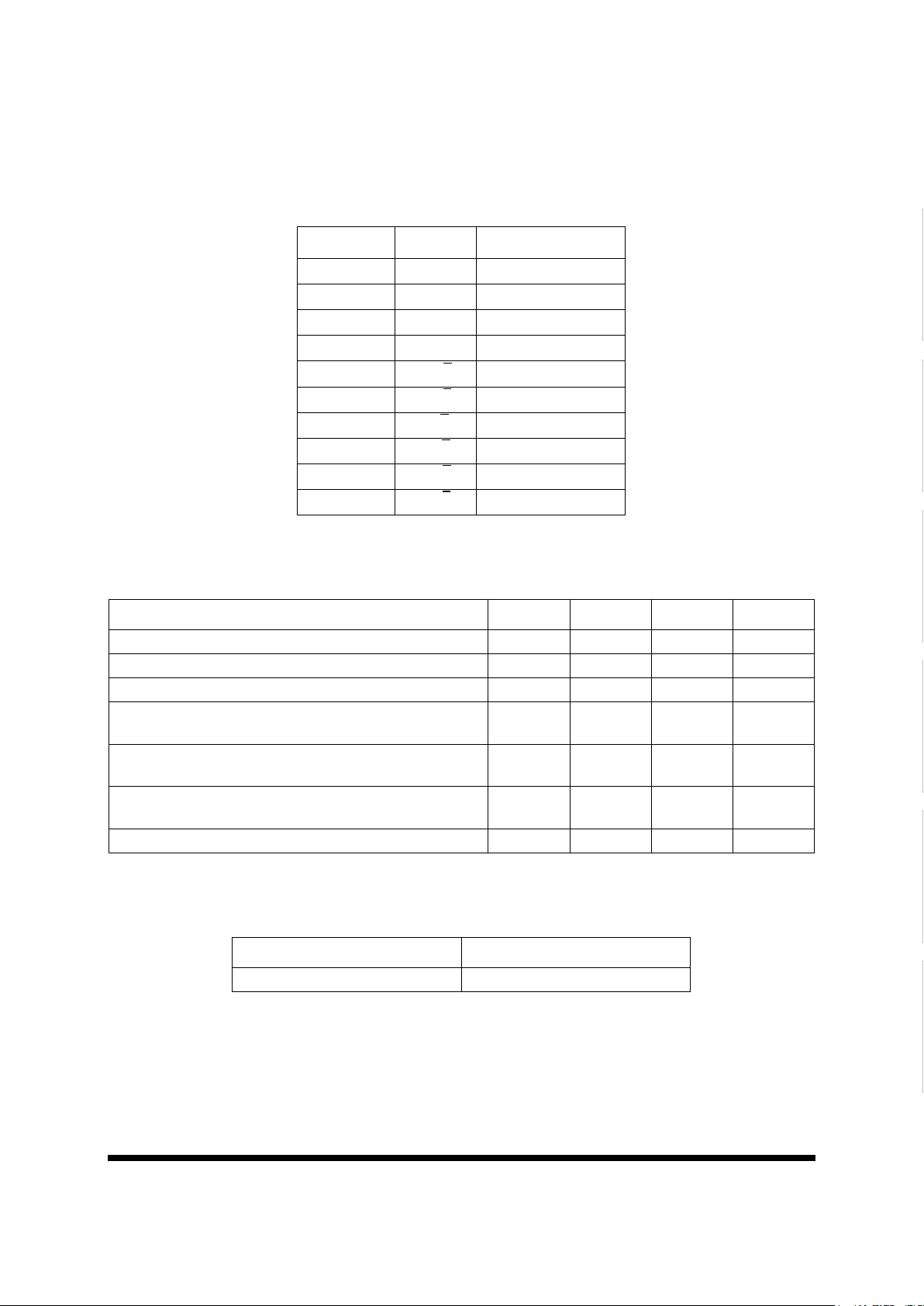
TABLE 1. 54HC4049 PINOUT DESCRIPTIONS
PIN SYMBOL DESCRIPTION
1VCCPower supply
8V
SS
Ground
13, 16 NC Not Connected
3, 5, 7, 9, 11, 14 A - F Inputs
2G = A
Inverted Output
4H = B
Inverted Output
6I = C
Inverted Output
10 J = D
Inverted Output
12 K = E
Inverted Output
15 L = F
Inverted Output
TABLE 2. 54HC4049 ABSOLUTE MAXIMUM RATINGS
PARAMETER SYMBOL MIN MAX UNIT
Storage Temperature T
S
-65 150 °C
Operating Temperature Range T
A
-55 125 °C
DC Supply Voltage V
CC
-0.5 7.0 V
DC Input Diode Current
For V
I
< -0.5V or VI > VCC +0.5V
I
IK
-20 +20 mA
DC Output Diode Current
For V
O
< -0.5V or VO > VCC +0.5V
I
OK
-20 +20 mA
DC Output Source or Sink Current per Output Pin
For V
O
> -0.5V or VO < VCC +0.5V
I
O
-25 +25 mA
DC V
CC
or Ground Current ICC or I
GND
-50 +50 mA
TABLE 3. DELTA LIMITS
PARAMETER VARIATION
I
CC
±10% of specified value in Table 5

Memory
3
All data sheets are subject to change without notice
©2001 Maxwell Technologies.
All rights reserved.
CMOS Logic Hex Inverting Buffers
54HC4049
12.20.01 Rev1
1000589
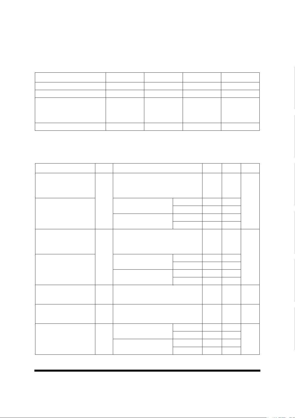
TABLE 4. 54HC4049 RECOMMENDED OPERATING CONDITIONS
PARAMETER SYMBOL MIN MAX UNIT
Supply Voltage V
CC
26V
DC Input or output Voltage V
I
, V
O
0VCCV
Input Rise and Fall Time
2V
4.5V
6V
-1000
500
400
ns
Temperature Range T
A
-55 125 °C
TABLE 5. 54HC4049 DC ELECTRICAL CHARACTERISTICS
(VCC = 5V ±10%, TA = -55 TO 125°C, UNLESS OTHERWISE SPECIFIED)
P
ARAMETER SYMBOL TEST CONDITIONS MIN MAX UNIT
High Level Output Voltage
CMOS Loads
V
OHVI
= VIH or VIL, IO = -0.02mA
V
CC
= 2V
V
CC
= 4.5V
V
CC
= 6V
1.9
4.4
5.9
--
--
--
V
High Level Output Voltage
TTL Loads
V
I
= VIH or VIL, IO = -4mA
V
CC
= 4.5V
+25°C 3.98 --
-55 to 125°C 3.7 --
V
I
= VIH or VIL, IO = -5.2mA
V
CC
= 6V
+25°C 5.48 --
-55 to 125°C 5.2 --
Low Level Output Voltage
CMOS Loads
V
OL
VI = VIH or VIL, IO = -0.02mA
V
CC
= 2V
V
CC
= 4.5V
V
CC
= 6V
0.1
0.1
0.1
V
Low Level Output Voltage
TTL Loads
V
I
= VIH or VIL, IO = 4mA
V
CC
= 4.5V
+25°C 0.26 --
-55 to 125°C 0.4
V
I
= VIH or VIL, IO = 5.2mA
V
CC
= 6V
+25°C 0.26 --
-55 to 125°C 0.4
High Level Input Voltage V
IH
VCC = 2V
V
CC
= 4.5V
V
CC
= 6V
1.5
3.15
4.2
--
--
--
V
Low Level Input Voltage V
IL
VCC = 2V
V
CC
= 4.5V
V
CC
= 6V
--
--
--
0.5
1.35
1.8
V
Input Leakage Current I
I
VCC = 6V, VI = VCC or GND +25°C -- ±0.1 µA
-55 to 125°C -- ±1
V
CC
= 6V, VI = 15V +25°C -- ±0.5
-55 to 125°C -- ±5
 Loading...