MAXWELL 54HC4046RP Datasheet

SEi - Radiation Hardened 54HC4046RP
Phase-Locked Loop
Features
• RAD-PAK
Against Natural Space Radiation
• Total Dose Hardness >100 krad (Si)
• Low Power Phase Lock Loop
• Package:
-16 Pin RAD-PAK Flat Package
-16 Pin RAD-PAK DIP
• Low Dynamic Power Consumption
- VCC = 4.5V
Technology Hardened
• Maximum VCO Operating Frequency
- 12 MHz (VCC = 4.5V)
• Fast Comparator Response Time
(VCC = 4.5V)
- Comparator I: 25 ns
- Comparator II: 30 ns
- Comparator III: 25 ns
• Screening per TM 5004
• QCI per TM5005
S Ei’s 54HC4046RP (RP for RAD-PAK
total dose tolerance. This device uses advanced CMOS technology to obtain high frequency operation. The
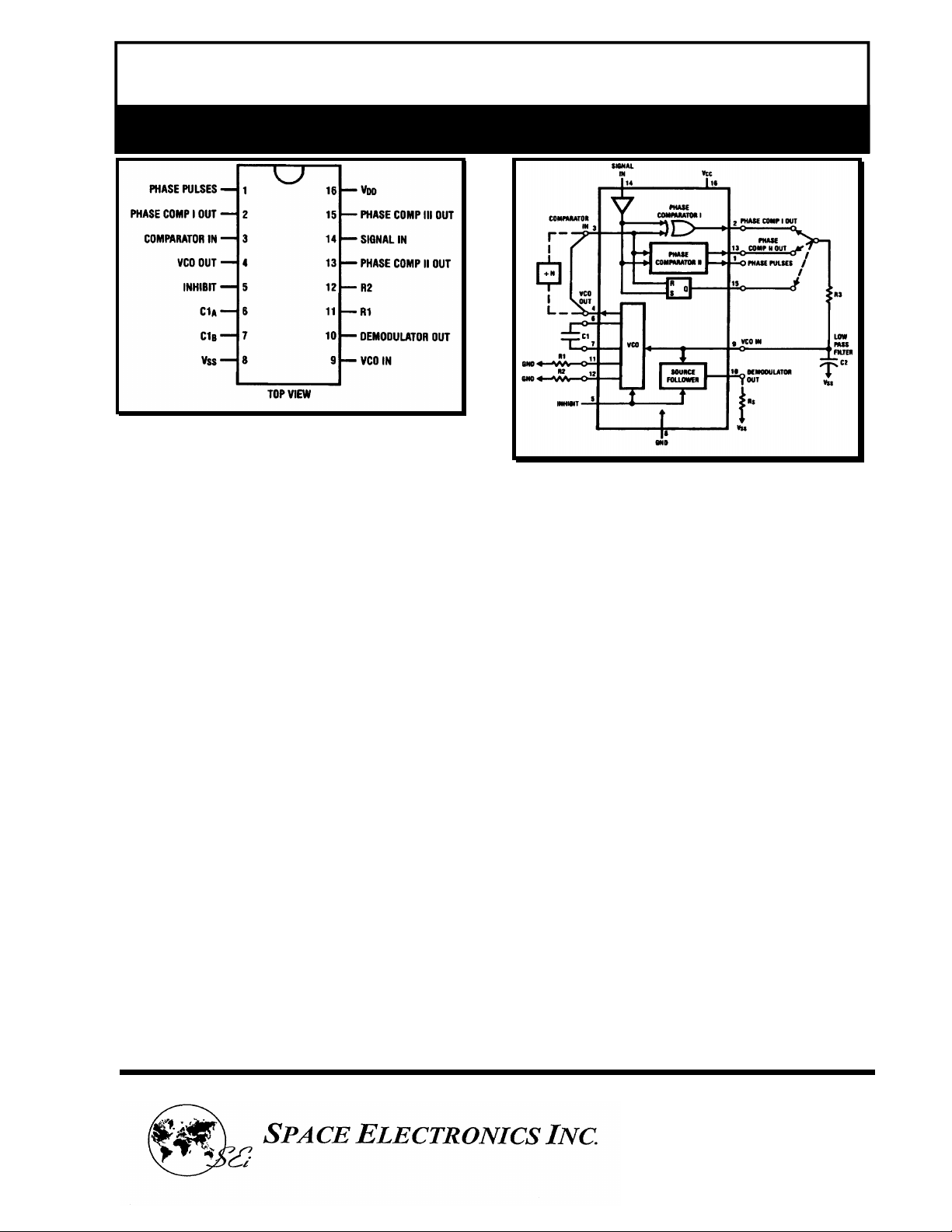
54HC4046RP contains a low power linear voltage controlled oscillator (VCO), a source follower, and three phase
comparators. The three phase comparators have a common signal input and a common comparator input. The
signal input has a self biasing amplifier allowing signals to be either capacitively coupled to the phase comparators with a small signal or directly coupled with standard input logic levels. Any one of the three comparators
feeds an external filter network, which in turn feeds the VCO input. This input is a very high impedance CMOS
input that also drives the source follower. An inhibit pin is provided to disable the VCO and the source follower,
providing a method of putting the IC in a low power state. Capable of surviving space environments, the
54HC4046RP is ideal for many satellite, spacecraft, and space probe missions. The radiation hardened RADPAK® technology incorporates radiation shielding in the microcircuit package. The 54HC4046RP is available in
Class S packaging and screening.
®
) high speed Phase Lock Loop microcircuit features a 100 kilorad (Si)
Specifications and design are subject to change without notice.
4031 Sorrento Valley Blvd.
San Diego, CA 92121
(619) 452-4167 Fax (619) 452-5499
Email: sales@spaceelectronics.com
--9.9--
http://www.spaceelectronics.com
1

SEi - Radiation Hardened 54HC4046RP
with this supply. Worst case V
Phase-Locked Loop
54HC4046RP ABSOLUTE MAXIMUM RATINGS
PARAMETER SYMBOL MIN MAX UNIT
Supply Voltage
DC Input Voltage
DC Output Voltage
Clamp Diode Current
DC Output Current, per pin
DC VCC or GND Current, per
pin
Storage Temperature Range
Power Dissipation
Note:
1/ Maximum Ratings are those values beyond which damage to the
device may occur.
2/ All voltages are referenced to ground, unless otherwise specified.
V
V
V
IIK, I
I
I
T
OUT
OUT
CC
STG
P
CC
IN
OK
D
-0.5 +7.0 V
-0.5
-0.5
-65 +150oC
1/ 2/
VCC+0.5
VCC+0.5
20 mA
±
+25 mA
50 mA
±
500 mW
V
V
54HC404SRP DC ELECTRICAL CHARACTERISTICS
PARAMETER SYMBOL TYP MAX UNIT
Minimum High Level Input Voltage
V
= 2.0V
CC
V
= 4.5V
CC
V
= 6.0V
CC
Maximum Low Level Input Voltage
V
= 2.0V
CC
V
= 4.5V
CC
V
= 6.0V
CC
Minimum High Level Output Voltage
V
= V
or V
IN
IH
|I
OUT|
V
CC
V
CC
V
CC
VIN=VIH or V
|I
OUT|
|I
OUT
Maximum Low Level Output Voltage
V
= V
IN
|I
OUT
V
CC
V
CC
V
CC
V
= VIH or V
IN
|I
OUT
|I
OUT
Input Current
VIN=VCC or GND @VCC=6.0V
Pin 3, 5, 9
Pin 14
Maximum Tri-State Output Leakage Current
(pin 13)
V
OUT
Maximum Quiescent Supply Current
VIN = VCC or GND , I
VIN = VCC or GND, Pin 14 Open, @VCC = 6.0V
Note:
1. For a power supply of 5V ± 10% the worst case output voltages (VOH and VOL) occur at 4.5V. Thus the 4.5V values should be used when designing
the higher voltage and so the 6.0V values should be used.
IL
20uA
≤
= 2.0V
= 4.5V
= 6.0V
IL
4.0mA @V
≤
| ≤ 5.2mA @V
or V
IH
| ≤ 20uA
= 3.0V
= 4.5V
= 6.0V
| ≤ 4.0mA @V
| ≤ 5.2mA @V
= VCC or GND @ VCC = 6.0V
= 4.5V
CC
= 6.0V
CC
IL
IL
= 4.5V
CC
= 6.0V
CC
= 0uA, @VCC = 6.0V
OUT
and VIL occur at V
IH
= 5.5V and 4.5V respectively. The worst case leakage current (IIN, ICC, and IOZ) occur for CMOS at
CC
V
IH
V
IL
V
OH
V
OL
I
IN
I
OZ
I
CC
54HC4046RP OPERATING CONDITIONS
PARAMETER SYMBOL MIN MAX UNIT
Supply Voltage V
DC Input or Output
Voltage
Operating
Temperature Range
Input Rise or Fall
Times
V
= 2.0V
CC
V
= 4.5V
CC
V
= 6.0V
CC
2.0
4.5
6.0
4.2
5.7
30
600
VIN, V
1
T
tr, t
CC
A
+2.0 +6.0 V
OUT
f
0 V
-55 +125
0
0
0
1.5
3.15
4.2
0.5
1.35
1.8
1.9
4.4
5.9
3.7
5.2
0.1
0.1
0.1
0.4
0.4
+1.0
100
+10 uA
160
3000
CC
1000
500
400
V
V
V
V
uA
uA
V
o
C
ns
--9.9--
2
4031 Sorrento Valley Blvd.
San Diego, CA 92121
(619) 452-4167 Fax (619) 452-5499
Email: sales@spaceelectronics.com
http://www.spaceelectronics.com

SEi - Radiation Hardened 54HC4046RP
Phase-Locked Loop
54HC4046RP AC ELECTRICAL CHARACTERISTICS
2/
PARAMETER SYMBOL TYP 3/ MAX UNIT
AC Coupled Input Sensitivity, Signal In
C(series) = 100 pF, fIN = 500 kHz
V
= 2.0V
CC
V
= 4.5V
CC
V
= 6.0V
CC
Maximum Output Rise and Fall Time
V
= 2.0V
CC
V
= 4.5V
CC
V
= 6.0V
CC
tr, t
f
200
250
350
110
22
19
PHASE COMPARATOR I
Maximum Propagation Delay
V
= 2.0V
CC
V
= 4.5V
CC
V
= 6.0V
CC
t
PHL
, t
PLH
300
60
51
PHASE COMPARATOR II
Maximum Tri-State Enable Time
V
= 2.0V
CC
V
= 4.5V
CC
V
= 6,0V
CC
Maximum Tri-State Enable Time
V
= 2.0V
CC
V
= 4.5V
CC
V
= 6,0V
CC
Maximum Tri-State Disable Time
V
= 2.0V
CC
V
= 4.5V
CC
V
= 6,0V
CC
Maximum Propagation Delay High to Low to Phase Pulses
V
= 2.0V
CC
V
= 4.5V
CC
V
= 6,0V
CC
t
PZL
t
PZH, tPHZ
t
PLZ
t
, t
PHL
PLH
340
68
57
360
72
61
360
72
61
380
75
64
PHASE COMPARATOR III
Maximum Propagation Delay
V
= 2.0V
CC
V
= 4.5V
CC
V
= 6.0V
CC
Maximum Power Dissipation Capacitance
All comparators, VIN = VCC and GND
t
PHL
, t
PLH
C
PD
130 pF
300
60
51
VOLTAGE CONTROLLED OSCILLATOR (operate @ VCC = 3.0v to 6.0V)
Maximum Operating Frequency
C1 = 50pF, R1 = 100Ω, R2 =
VCC = 4.5V
VCC = 6.0V
V
= VCC, C1 = 0pF, R1 = 100Ω, V
COin
VCC = 4.5V
VCC = 6.0V
Duty Cycle 50 %
∞
= V
COin
CC
f
MAX
7
11
12
14
DEMODULATOR OUTPUT
Offset Voltage (V
RS = 20kΩ, V
Offset Variation
RS = 20kΩ, V
V
= 1.75V
COin
V
= 2.25V
COin
V
= 2.75V
COin
Note:
2/ V
3/ TA = 25oC.
- V
CC
CC
COin
= 4.5V
= 4.5V
CC
)
dem
= 2.0 to 6.0V, CL = 50pF, tr = tf = 6ns (unless otherwise specified.)
1.6 V
0.65
0.1
0.75
mV
ns
ns
ns
ns
ns
ns
ns
MHz
V
--9.9--
3
4031 Sorrento Valley Blvd.
San Diego, CA 92121
(619) 452-4167 Fax (619) 452-5499
Email: sales@spaceelectronics.com
http://www.spaceelectronics.com
 Loading...