

Page 1
9XTend™ OEM RF Module
Firmware versions supported in this
manual:
Standard firmware: 2x4x, 2x6x
DigiMesh firmware: 8x2x (see Chapter
5)
MaxStream, Inc.
355 South 520 West
Lindon, UT 84042
90000958_B
2010.02.26
Page 2

9XTend™ OEM RF Module - Product Manual v2.x6x
MaxStream, Inc. All rights reserved
The contents of this manual may not be tran
by any means without the permission of MaxStream, Inc.
XTend™ is a trademark of Digi International, Inc.
AES Encryption Source Code
© 2008 Dr. Brian Gladman, Worcester, UK. All rights reserved.
Conditions:
- Distributions of AES source code include the above copyright notice, this list of
conditions and disclaimer.
- Distributions in binary form include the above copyright notice, this list of conditions and disclaimer in the documentation and/or oth
ed or reproduced in any form or
er associated materials.
- The copyright holder's name is not used to endorse products built using this
ware without specic permission.
Alternatively, provided that this notice is retained in full, this product may be distributed under the terms of the GNU General Public License (GPL), in which case
the provisions of the GPL apply INSTEAD OF those given above.
Disclaimer - This AES so
ranties in respect of its properties, including, but not limited to, correctness and/or
for purpose.
Technical Support: Phone: (801) 765-9885
ware is provided 'as is' with no explicit or implied war-
Live Chat: ww
E-support:
w.digi.com
w.digi.com/support/eservice/eservicelogin.jsp
© 2010 MaxStream, Inc. ii
Page 3

9XTend™ OEM RF Module – Product Manual v2.x6x
Contents
1. 9XTend OEM RF Module 4
Key Features 4
Worldwide Acceptance 4
Specifications 5
Pin Signals 6
Electrical Characteristic 7
Timing Specifications 7
Mechanical Drawings 8
9noitarepO eludoM FR .2
Serial Communications 9
UART Data Flow 9
Flow Control 10
Transparent Operation 11
API Operation 11
DigiMesh Operation 11
Modes of Operation 12
Idle Mode 12
Transmit Mode 12
Receive Mode 13
Shutdown Mode 14
Sleep Mode 14
Command Mode 16
3. RF Module Configuration 19
Programming Examples 19
AT Commands 19
Binary Commands 19
Command Reference Table 20
Command Descriptions 22
API Operation 41
API Frame Specifications 41
API Types 42
4. RF Communication Modes 44
Addressing 45
Address Recognition 45
Basic Communications 46
Streaming Mode (Default) 46
Multi-transmit Mode 47
Repeater Mode 48
Polling Mode (Basic) 51
Acknowledged Communications 52
Acknowledged Mode 52
Polling Mode (Acknowledged) 54
55™hseMigiD .5
Introduction 55
DigiMesh Feature Set 55
Data Transmission and Routing 55
Unicast Addressing 55
Broadcast Addressing 56
Routing 56
Route Discovery 56
RF Module Configuration 56
AT Commands 56
AT Command Reference Table 57
API Operation 62
API Frame Specifications 62
6. Appendix A: Agency Certifications 66
FCC (United States) Certification 66
OEM Labeling Requirements 66
FCC Notices 66
Limited Modular Approval 67
FCC-approved Antennas 67
Labeling Requirements 70
C-TICK (Australia) Certification 70
Power Requirements 70
7. Appendix B: Development Guide 71
Development Kit Contents 71
Interfacing Hardware 71
XTIB-R RS-232/485 Interface Board 72
Automatic DIP Switch Configurations 73
Adapters 74
Interfacing Protocols 76
RS-232 Operation 76
RS-485 (2-wire) Operation 78
RS-485 (4-wire) & RS-422 Operation 79
X-CTU Software 81
Installation 81
Serial Communications Software 81
8. Appendix C: Additional Information 82
1-Year Warranty 82
Ordering Information 82
Contact Digi 83
© 2010 MaxStream, Inc. tial & Proprietary - All Rights Reserved iii
Page 4

1. 9XTend OEM RF Module
The 9XTend OEM RF Module was engineered to provide OEMs an
easy-to-use RF solution that provides reliable delivery of critical
data between remote devices. The module transfers a standard
asynchronous serial data stream, operates within the ISM 900 MHz
frequency band and sustains up to 115.2 Kbps data throughput.
Key Features
Long Range Data Integrity
1 Watt Power Output (variable 1mW - 1W)
Range (@9,600 bps throughput data rate):
Indoor/Urban: up to 3000’ (900 m)
Outdoor RF line-of-sight:
up to 14 miles (22 km) w/dipole antenna
Outdoor RF line-of-sight:
up to 40 miles (64 km) w/high-gain antenna
Range (@115,200 bps throughput data rate):
Indoor/Urban: up to 1500’ (450 m)
Outdoor RF line-of-sight:
up to 7 miles (11 km) w/dipole antenna
Outdoor RF line-of-sight:
up to 20 miles (32 km) w/high-gain antenna
Continuous RF data stream up to 115,200 bps
Receiver Se
–100 dBm (@ 115200 baud)
Advanced Networking & Security
True Peer-to-Peer (no Master device required),
Point-to-Point, Point-to-Multipoint & Multidrop
Retries and Acknowledgements
FHSS (Frequency Hopping Spread Spectrum)
10 hopping channels, each with over 65,000
unique network addresses available
256-bit AES Encryption
128-bit AES for international variant
nsitivity: -110 dBm (@ 9600 baud),
Low Power
2.8 - 5.5 V Supply Voltage
Pin, Serial Port and Cyclic
software sleep modes supported
Shutdown pin enables hardware sleep m
that draws only 5 μA (typical)
Easy-to-Use
No configuration necessary for out-of box
RF communications
Free X-CTU Software
(Testing and configuration software)
RF Modules easily configured using
standard AT & binary commands
Transparent Operation
(Wireless links replace serial wires)
API Operation
(Frame-based communications)
Portable
(small form-factor easily designed into
a wide range of data systems)
Software-selectable I/O interfacing rates
Multiple data formats supported
(parity, start and stop bits, etc.)
XII™ Interference Immunity
No Master/Slave setup dependencies
ode
Worldwide Acceptance
FCC Approved (USA) Refer to Appendix A [p66] for FCC Requirements.
Systems that include XTend RF Modules inherit MaxStream’s Certifications.
ISM (Industrial, Scientific & Medical) license-free 902-928 MHz frequency band
Manufactured under ISO 9001:2000 registered standards
ESD (Electrostatic Discharge) immunity - ESD-hardened and IEC1000-4-2 (Level 4) tested
9XTend OEM RF Modules are optimized for use in the US, Canada, and Australia
(contact Digi for complete list of agency approvals).
© 2010 MaxStream, Inc. 4
Page 5

9XTend™ OEM RF Module - Product Manual v2.x6x
Specifications
Table 1-01. 9XTend-PKG-R OEM RF Module
9XTend 900 MHz OEM RF Module Specifications
Performance @9600 bps Throughput Data Rate @115200 bps Throughput Data Rate
Transmit Power Output
(software selectable using PL command)
Outdoor
RF line-of-sight Range
Interface Data Rate
(software selectable using BD command)
Throughput Data Rate
(software selectable
Power Requirements
Idle Currents
Networking & Security
Frequency 902-928 MHz
Physical Properties
Weight 0.64 oz. (18 g)
Connector 20-pin
Antenna
Certifications (partial list)
using BR command)
itisneS revieceR
( peels cilcyc ces 61
aC lennahC
Up to 14 miles (22 km) w/ dipole antenna
Up to 40 miles (64 km) w/ high-gain antenna
aler
”evalS/retsaM“( reeP-ot-reePseigolopoT krowteN detroppuS tionship not required), Point-to-Point, Point-to-Multipoint
x ”83.2 x ”44.1eziS draoB eludoM FR 0.20” (3.65 cm x 6.05 cm x 0.51 cm)
04-erutarepmeT gnitarepO to 85º C (industrial)
Up to 7 miles (11 km) w/ dipole antenna
Up to 20 miles (32 km) w/ high-gain antenna
2 – 0021spb 004032 – 0021
spb 002,511spb 006,9
spb 000,521spb 000,01etaR ataD FR
mBd 001-mBd 011-ytiv
Am 08tnerruC evieceR
lacipyt Aμ 5nwoD rewoP edoM nwodtuhS
Aμ 741nwoD rewoP peelS niP
Am 8.0 - 3.0)8=MS
Am 4.1 - 4.0)7=MS( peels cilcyc ces 8
Am 6.2 - 6.0)6=MS( peels cilcyc ces 4
Am 8.
4 - 9.0)5=MS( peels cilcyc ces 2
Am 7.8 - 6.1)4=MS( peels cilcyc ces 1
)murtcepS daerpS gnippoH ycneuqerF( SSHFmurtcepS daerpS
)gniyeK tfihS ycneuqerF( KSFnoitaludoM
seicneuqerf 05 erahs secneuqes poh 01yticap
refeR – noitpyrcnE SEA tib-652noitpyrcnE to the KY Command [p29] to implement
XCMM ro )AMS ytiralop-esreveR( AMSPRsnoitpO rotcennoC
decnalabnu smho 05ecnadepmI
DNETX9-RUO742.51 traP CCF
DNETX9-A4124)CI( adanaC yrtsudnI
ttaW 1 - Wm1ttaW 1 - Wm1
)m 054( ’0051 ot pU)m 009( ’0003 ot pUegnaR nabrU/roodnI
*
spb 00403
**
* Throughput is always lower than the RF data rate due to overhead.
Table 1-02. XTend OEM RF Module Speccations - Relative to user-selected TX Power Output
Power Requirements (Supply voltage and TX currents relative to each TX Power Output option)
Transmit Power Output 1 mW 10 mW 100 mW 500 mW * 1 W *
CDV 5.5 - 57.4CDV 5.5 - 0.3CDV 5.5 - 8.2egatloV ylppuS
Transmit Current (5 V) typical 110 mA 140 mA 270 mA 500 mA 730 mA
Transmit Current (3.3 V) typical 90 mA 110 mA 260 mA 600 mA **
* If the supply voltage for a given power se ing is lower than the minimum supply voltage requirement (as shown in Table 1-02), the
TX Power Output will decrease to the highest power level se
** 1W Power Output is not supported when using a 3.3 supply voltage.
ing given the current supply voltage.
© 2010 MaxStream, Inc. 5
Page 6

9XTend™ OEM RF Module - Product Manual v2.x6x
Pin Signals
Figure 1-01. XTend OEM RF Module Pin Numbers
Table 1-03. Pin Signal Descriptions
Pin
Number
10
11 CONFIG
(Low-asserted signals distinguished with a horizontal line over signal name.)
Mnemonic I/O
1GND- - yesGround
2 VCC I - yes Power: 2.8 - 5.5 VDC
3
4 TX
5DII yes yes
6DOOyes -
7 SHDN
8 GPI2 / SLEEP I yes -
9
GPO2 /
RX LED
_PWR O yes -
GPO1 / CTS
RS-485 TX_EN
GPI1 / RTS
/
/
CMD
/ RSSI
High Impedance
during Shutdown
Oyes -
Ino yes
Oyes -
Iyes -
I* no -
O* no -
Must
Connect
General Purpose Output 2: <Default (CD=2)> Pin is driven low. Refer to the CD
Command [p24] for other configuration options.
RX LED: Pin is driven high during RF data reception; otherwise, the pin is driven
low. Refer to the CD Command [p24] to enable.
Transmit_Power: Pin pulses low during RF transmission; otherwise, the pin is
driven high to indicate power is on and the module is not in Sleep or Shutdown
Mode.
Data In: Serial data entering the module (from the UART host). Refer to the Serial
Communications [p9] section for more information.
Data Out: Serial Data exiting the module (to the UART host). Refer to the Serial
Communications [p9] section for more information.
Shutdown: Pin is driven high during operation and low during Shutdown.
Shutdown enables the lowest power mode (~5 μA) available to the module. Refer
to the Shutdown Mode [p14] section for more information.
General Purpose Input 2: reserved for future use
SLEEP: By default, SLEEP is not used. To configure this pin to enable Sleep
Modes, refer to the Sleep Mode [p14], SM Command [p37] & PW Command [p32]
sections.
General Purpose Output 1: reserved for future use
(Clear-to-Send): <Default (CS=0)> When pin is driven low, the UART host
CTS
is permitted to send serial data to the module. Refer to the Serial Communications
[p9] & CS Command [p25] sections for more information.
RS-485 Transmit Enable: To configure this pin to enable RS-485 half and fullduplex communications. Refer to the Serial Communications [p9] & CS Command
[p25] sections.
General Purpose Input 1: reserved for future use
(Request-to-Send): By default, is not used. To configure this pin to
RTS
regulate the flow of serial data exiting the module, refer to the Serial
Communications [p9] & RT Command [p36] sections.
CMD (Command): By default, CMD is not used. To configure this pin to enable
binary command programming, refer to the Binary Commands [p17] & RT
Command [p36] sections.
Configuration: Pin can be used as a backup method for entering Command
Mode during power-up. Refer to the Command Mode [p17] section for more
information.
Receive Signal Strength Indicator: By default, pin is used as an RSSI PWM
output after at the conclusion of the power-up sequence. Refer to the RP
Command [p35] for more information. The PWM output is 2.8V-level.
Function
tcennoc ton od / devreser02-21
* RF module has 10K internal pull-up resistor
Note: When integrating the module with a Host PC board, all lines not used should be left disconnected (floating).
© 2010 Digi Internatonal, Inc. 6
Page 7
9XTend™ OEM RF Module - Product Manual v2.x6x
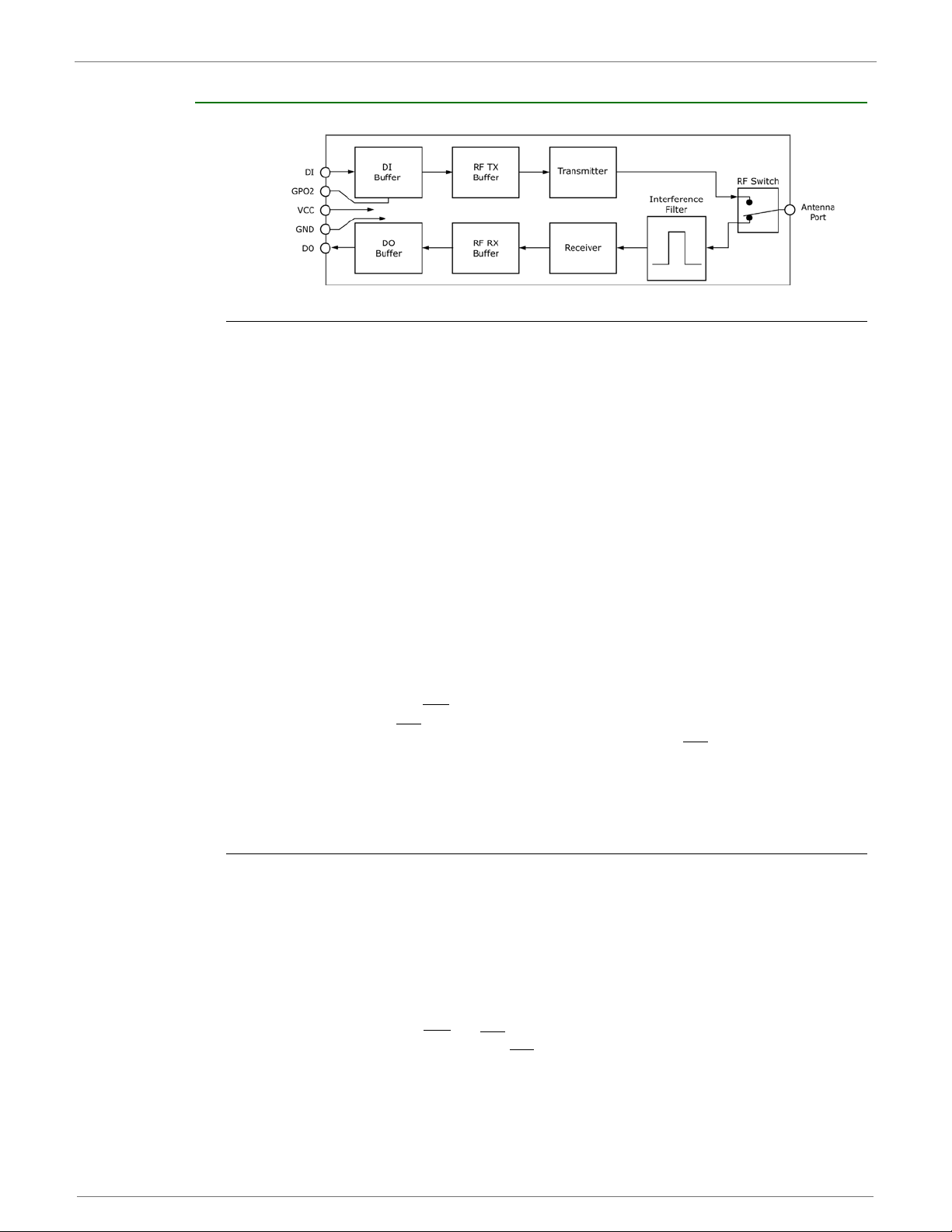
Electrical Characteristic
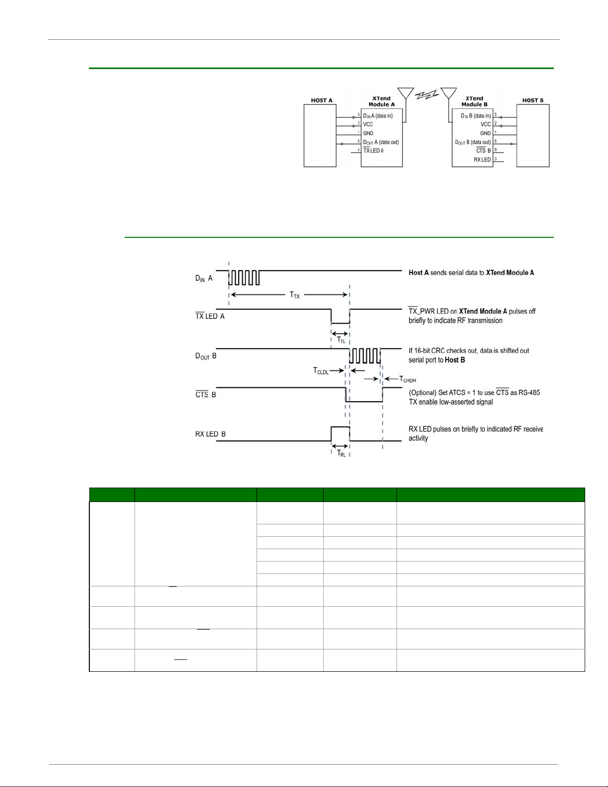
Figure 1-02. System Block Diagram
Basic RF Link between Hosts
The data flow sequence is initiated when the first byte of data is received in the DI Buffer of the
transmitting module (XTend RF Module A). As long as XTend RF Module A is not already receiving
RF data, data in the DI Buffer is packetized then transmitted over-the-air to XTend RF Module B.
Timing Specifications
Figure 1-03. Timing Specations (‘A’ and ‘B’ refer to Figure 1-02)
Table 1-04. AC Characteristics (Symbols correspond with Figure 1-02 and Figure 1-03, ATSY Parameter = 0)
Symbol Description Sleep Mode 115200 Baud Rate 9600 Baud Rate
SM = 0
(No sleep)
T
T
T
T
CHDH
TX
T
TL
RL
CLDL
Latency from the time data is
transmitted until it is received.
Time that TX_PWR pin (pin 4) is driven
low
Time that RX LED (pin 3)
is driven high
Time starting when CTS goes low until
the first bit appears on DOUT
Time after last bit of data until
CTS
goes high
© 2010 Digi Internatonal, Inc. 7
cesm 49cesm 4.9
ces 61ces 618 = MS
ces 8ces 87 = MS
ces 4ces 46 = MS
ces 2ces 25 = MS
ces 1ces 14 = MS
cesm 6.92cesm 54.2--
cesm 2.72cesm 62.2--
cesμ 57cesμ 44--
cesμ 7cesμ 7--
Page 8
9XTend™ OEM RF Module - Product Manual v2.x6x
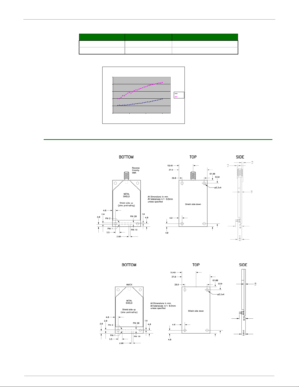
Table 1-05. DC Characteristics (Vcc = 2.8 - 5.5 VDC)
Symbol Parameter Condition
V
OL
V
OH
Figure 1-04. Input Thresholds vs. Supply Voltage
Input thresholds vs. supply voltage
2.5
2
1.5
1
I/O Voltage
0.5
0
2.5 3.5 4.5 5.5
Mechanical Drawings
Figure 1-05. Mechanical drawings of the XTend OEM RF Module (w/RPSMA Connector)
Output Low Voltage
Output High Voltage
Vcc
V(IL )
V(IH)
V
OL
= V
V
OH
SUPPLY
= 0.33V (IO = 6 mA)
- 0.7V (-IO = 6 mA)
Figure 1-06. Mechanical drawings of the XTend OEM RF Module (w/MMCX Connector)
© 2010 Digi Internatonal, Inc. 8
Page 9
2. RF Module Operation
WARNING: When operating at 1 Watt power output, observe a minimum separation distance of 2' (0.6m) between
modules. Transmitting in close proximity of other modules can damage module front ends.
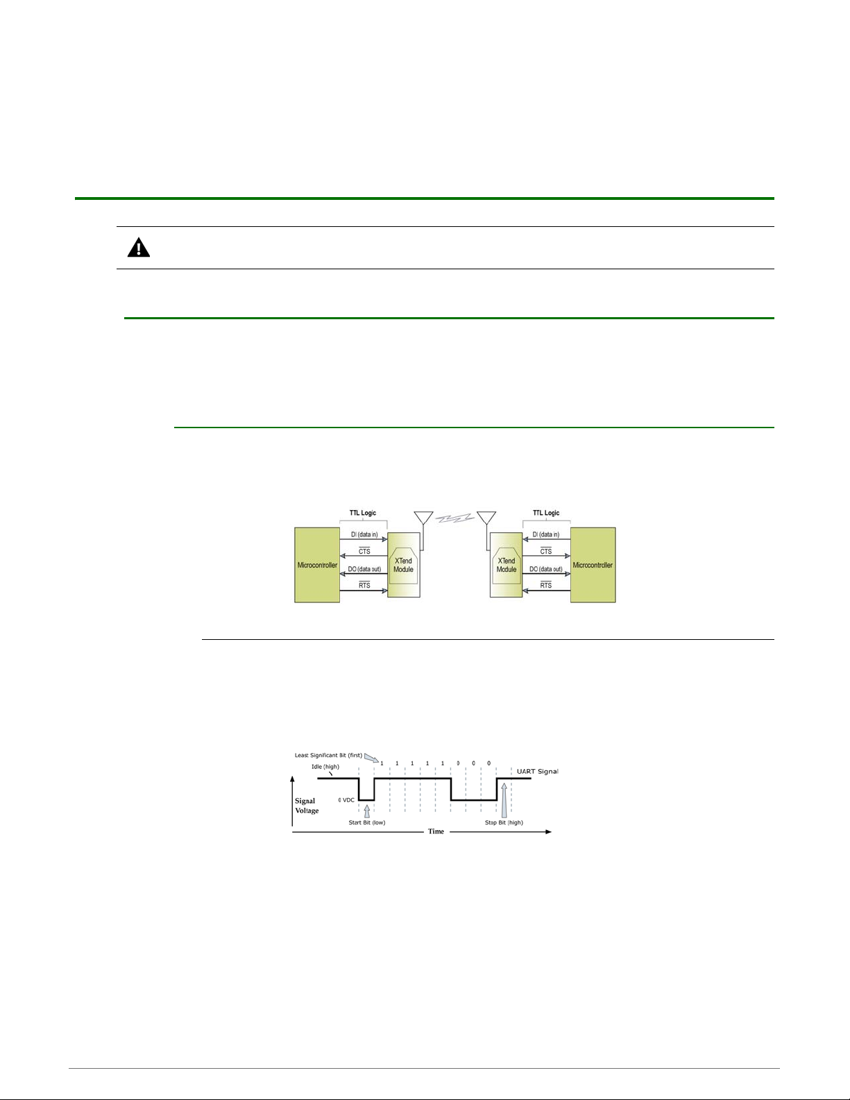
Serial Communications
The XTend OEM RF Modules interface to a host device through a TTL-level asynchronous serial
port. Through its serial port, the module can communicate with any UART voltage compatible
device or through a level translator to any serial device (For example: RS-232/485/422 or USB
interface board).
UART Data Flow
Devices that have a UART interface can connect directly to the pins of the RF module as shown in
the figure below.
Figure 2-01. System Data Flow Diagram in a UART-interfaced environment
(Low-asserted signals distinguished with horizontal line over signal name.)
Serial Data
Data enters the module UART through the pin 5 as an asynchronous serial signal. The signal
should idle high when no data is being transmitted.
Each data byte consists of a start bit (low), 8 data bits (least significant bit first) and a stop bit
(high). The following figure illustrates the serial bit pattern of data passing through the module.
Figure 2-02. UART data packet 0x1F (decimal number "31") as transmied through the RF module
The module UART performs tasks, such as timing and parity chec
communications. Serial communications depend on the two UARTs to be configured with compatible settings (baud rate, parity, start bits, stop bits, data bits).
Example Data Format is 8-N-1 (bits - parity - # of stop bits)
king, that are needed for data
© 2010 Digi International Inc. 9
Page 10
9XTend™ OEM RF Module - Product Manual v2.x6x
Flow Control
Figure 2-03. Internal Data Flow Diagram (The ve most commonly-used pin signals shown)
DI (Data In) Buffer and Flow Control
When serial data enters the module through the DI pin (pin 5), the data is stored in the DI Buffer
until it can be processed.
When the RB and RO parameter thresholds are satisfied (refer to ‘Transmit Mode’ section for more
information), the module attempts to initialize an RF connection. If the module is already receiving
RF data, the serial data is stored in the module's DI Buffer. The DI buffer stores at least 2.1 KB. If
the DI buffer becomes full, hardware or software flow control must be implemented in order to
prevent overflow (loss of data between the host and RF module).
How to eliminate the need for flow control:
1. Send messages that are smaller than the DI buffer size. The size of the DI buffer varies
according to the packet size (PK parameter) and the parity setting (NB parameter) used.
2. Interface at a lower baud rate (BD parameter) than the RF data rate (BR parameter).
Two cases in which the DI Buffer may become full and possibly overflow:
1. If the serial interface data rate is set higher than the RF data rate of the module, the module will recei
2. If the module is receiving a continuous stream of RF data or if the module is monitoring
data on a network, any serial data that arrives on the DI pin (pin 5) is placed in the DI
Buffer. The data in the DI buffer will be transmitted over-the-air when the module no longer
detects RF data in the network.
Hardware Flow Control (CTS
the module de-asserts CTS
(Flow Control Threshold) and CS (GPO1 Configuration) Commands]. CTS
DI Buffer has 34 bytes of memory available.
Software Flow Control (XON). XON/XOFF software flow control can be enabled using the FL
(Software Flow Control) Command. This option only works with ASCII data.
DO (Data Out) Buffer
When RF data is received, the data enters the DO buffer and is sent out the serial port to a host
device. Once the DO Buffer reaches capacity, any additional incoming RF data is lost. The DO
buffer stores at least 2.1 KB.
Two cases in which the DO Buffer may become full and possibly overflow:
1. If the RF data rate is set higher than the interface data rate of the module, the module will
receive data from the transmitting module faster than it can send the data to the h
2. If the host does not allow the module to transmit data out from the DO buffer because of
being held off by hardware or software flow control.
ve data from the host faster than it can transmit the data over-the-air.
). When the DI buffer is 17 bytes away from being full; by default,
(high) to signal to the host device to stop sending data [refer to FT
is re-asserted after the
ost.
Hardware Flow Control (RTS
not be sent out the DO Buffer as long as RTS
Software Flow Control (XOFF). XON/XOFF software flow control can be enabled using the FL
(Software Flow Control) Command. This option only works with ASCII data.
). If RTS is enabled for flow control (RT Parameter = 2), data will
(pin 10) is de-asserted.
© 2010 Digi Internatonal, Inc. 10
Page 11

9XTend™ OEM RF Module - Product Manual v2.x6x
Transparent Operation
By default, XTend RF Modules operate in Transparent Mode. The modules act as a serial line
replacement - all UART data received through the DI pin is queued up for RF transmission. When
RF data is received, the data is sent out the DO pin.
When the RO (Packetization Timeout) parameter threshold is satisfied, the module attempts to initialize an RF transmission. If the module cannot immediately transmit (for instance, if it is already
receiving RF data), the serial data cont
sent at any RO timeout or when the maximum packet size is received.
The module operates as described above unless the Command Mode Sequence is detected. The
Command Mode Sequence consists of three copies of the command sequence character [CC
parameter] surrounded by the before and after guard times [BT & AT parameters].
If the DI buffer becomes full, hardware or software flow control must be implemented in order to
prevent overflow (loss of data between the host and module).
API Operation
API (Application Programming Interface) Operation is an alternative to the default Transparent
Operation. The API is frame-based and extends the level to which a host application can interact
with the networking capabilities of the module. When in API mode, all data entering and leaving
the RF module is contained in frames that define operations or events within the module.
Transmit Data Frames (received through the DI (Data In) pin) include:
16-bit address
Receive Data Frames (sent out the DO (D
Showing a received RF packet (16 bits only)
Response to a TX (Transmit) packet
Showing events such as hardware reset, watchdog reset, asynchronous events, etc.
The module will send data frames to the application containing status packets; as well as source,
RSSI and payload information from received data packets.
API operation option facilitates many operations such as the examples cited below:
-> Change destination addresses without having to enter command mode
-> Receive success/failure status of each RF packet
-> Identify the source address of each received packet
inues to be stored in the DI Buffer. Data is packetized and
ata Out) pin) include:
To implement API operations, refer to ‘API Operation’ sections [p40].
DigiMesh Operation
XTend OEM RF Modules containing firmware version 8020 (or above) now feature DigiMesh mesh
networking support. Mesh networking allows messages to be routed through several different
9XTend nodes to a final destination node. This firmware load allows OEMs and system integrators
to bolster their networks with the self-healing attributes of mesh networking. In the event that
one RF connection between nodes is lost (due to power-loss, environmental obstructions, etc.)
critical data can still reach its destination due to mesh networking capabilities embedded
module. Transparent or API operations can be used in conjunction with the mesh networking
topology.
© 2010 Digi Internatonal, Inc. 11
inside the
Page 12
9XTend™ OEM RF Module - Product Manual v2.x6x
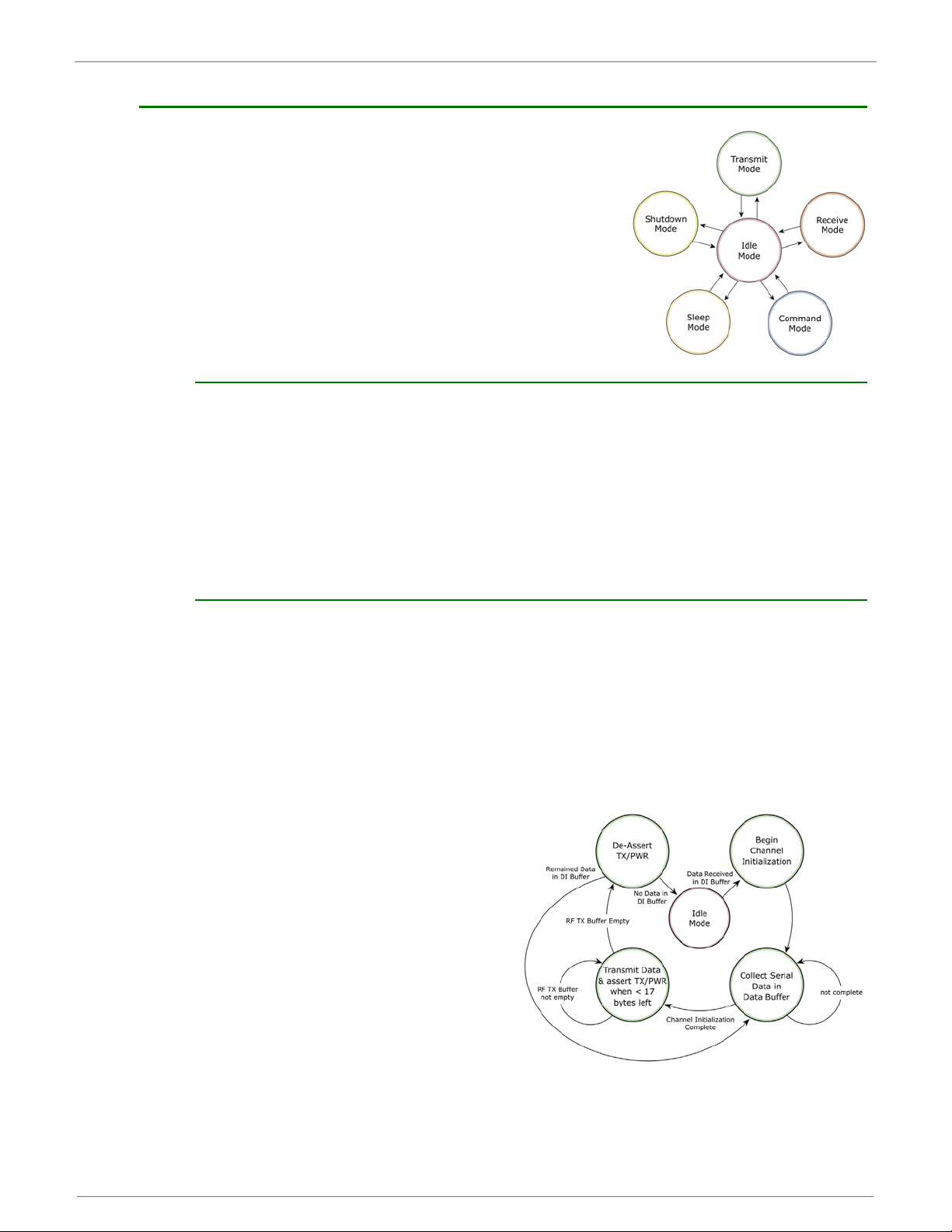
Modes of Operation
XTend RF Modules operate in six modes.
Figure 2-04. XTend RF Module Modes of Operation
Idle Mode
When not receiving or transmitting data, the RF module is in Idle Mode. The module shifts into the
other modes of operation under the following conditions:
Transmit Mode: Serial data is received in the DI Buffer
Receive Mode: Valid RF data is received through the antenna
Shutdown Mode: Shutdown condition is met
Sleep Mode: Sleep Mode condition is met
Command Mode: Command Mode Sequence is issued
The module automatically transitions back to Idle Mode after responding to these conditions.
(RF modules can only be in one mode at a time)
Transmit Mode
When the first byte of serial data is received from the UART in the DI buffer, the module attempts
to shift to Transmit Mode and initiate an RF connection with other modules. After transmission is
complete, the module returns to Idle Mode.
RF transmission begins after either of the following criteria is met:
1. RB bytes have been received by the UART and are pending for RF transmission.
[Refer to the RB (Packetization Threshold) Command]
2. At least one character has been received by the UART and is pending for RF transmission;
and RO character times of silence been observed on the UART.
[Refer to the RO (Packetization Timeout) Command]
Figure 2-05. Transmit Mode Data Flow
The character timeout trigger can be
disabled by setting RO to zero. In this
case, transmission will not begin until
RB bytes have been received
pending for RF transmission. The RB
parameter may be set to any value
between 1 and the RF packet size [refer
to PK (Max RF Packet Size) parameter],
inclusive. Note that transition to Transmit Mode cannot take place during RF
reception; the RF reception must complete before the radio can transition into
Transmit Mode.
If RB or RO conditions are met, the
module initializes a communications channel. Serial data in the DI buffer is grouped into RF packets (up to 2048 bytes in each pa
ted over-the-air until the DI buffer is empty.
and are
cket, refer to PK Command), converted to RF data and is transmit-
© 2010 Digi Internatonal, Inc. 12
Page 13
9XTend™ OEM RF Module - Product Manual v2.x6x
Channel initialization is the process of sending an RF initializer that synchronizes receiving modules with the transmitting module. During channel initialization, incoming serial data accumulates
in the DI buffer.
RF data, which includes the payload data, follows the RF initializer. The payload includes up to the
maximum packet size (PK Command) bytes. As the TX module nears the end of the transmission,
it inspects the DI buffer to see if more data exists to be transmitted. This
than PK bytes were originally pending in the DI buffer or if more bytes arrived from the UART after
the transmission began. If more data is pending, the transmitting module assembles a subsequent
packet for transmission.
Refer to the ‘RF Communication Modes’ section to view state diagrams that illustrate channel initialization and the sequence of events that follow.
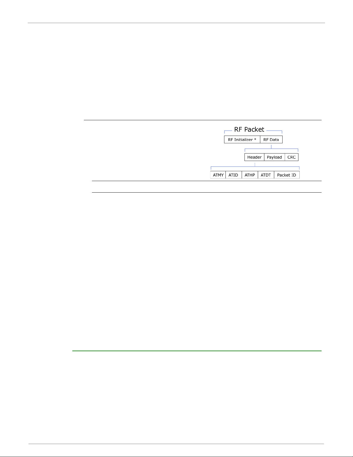
RF Packet
Figure 2-06. RF Packet Components
could be the case if more
* When streaming multiple RF packets, the RF Initializer is only sent in front of the first packet.
RF Initializer
An RF initializer is sent each time a new connection sequence begins. The RF initializer contains
channel information that notifies receiving modules of information such as the hopping pattern
used by the transmitting module. The first transmission always sends an RF initializer.
An RF initializer can be of various lengths depending on the amount of time determined to be
required to prepare a receiving module. For example, a wake
used to wake remote modules from Sleep Mode (Refer to the FH, LH, HT and SM Commands for
more information). The length of the wake-up initializer should be longer than the length of time
remote modules are in cyclic sleep.
Header
The header contains network addressing information that filters incoming RF data. The receiving
module checks for matching a Hopping Channel, VID and Destination Address. Data that does not
pass through all three network filter layers is discarded.
Refer to the ‘Addressing’ section of the “RF Communication Modes
CRC (Cyclic Redundancy Check)
To verify data integrity and provide built-in error checking, a 16-bit CRC (Cyclic Redundancy
Check) is computed for the transmitted data and attached to the end of each RF packet. On the
receiving end, the receiving module computes the CRC on all incoming RF data. Received data that
has an invalid CRC is discarded [refer to the ‘Receive Mode’ section].
-up initializer is a type of RF initializer
” chapter for more information.
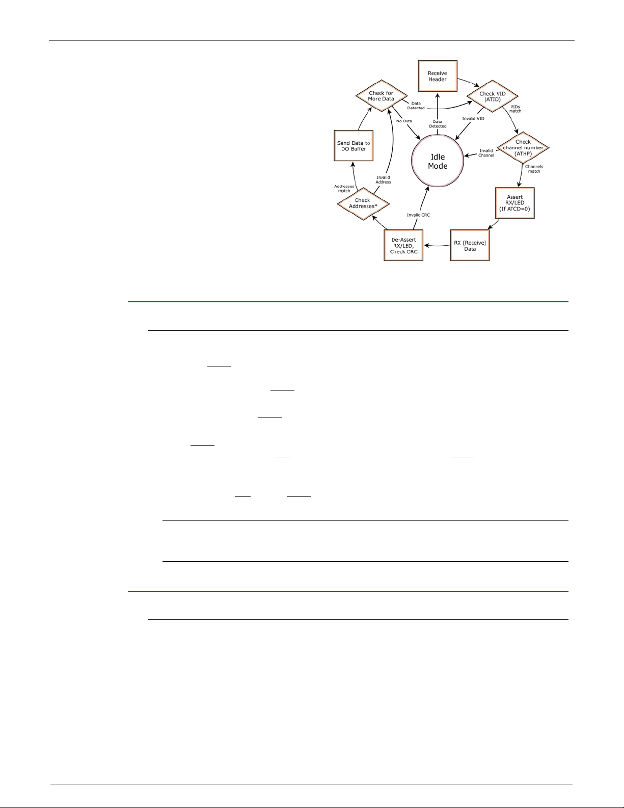
Receive Mode
If a module detects RF data while operating in Idle Mode, the module transitions to Receive Mode
to start receiving RF packets. Once a packet is received, the module checks the CRC (cyclic redundancy check) to ensure that the data was transmitted without error. If the CRC data bits on the
incoming packet are invalid, the packet is discarded. If the CRC is valid, the packet proceeds to the
DO Buffer.
© 2010 Digi Internatonal, Inc. 13
Page 14
9XTend™ OEM RF Module - Product Manual v2.x6x
Figure 2-07. Receive Mode Data Flow
* Refer to the ‘Address Recognition’ section for more information regarding
address recognition.
The module returns to Idle Mode
when valid RF data is no longer
detected or after an error is
detected in the received RF data. If
serial data is stored in the DI
buffer while the module is in
Receive Mode, the serial data will
be transmitted after the module is
finished receiving data and returns
to Idle Mode.
Shutdown Mode
Hardware Sleep
For applications where power consumption must be kept to a minimum during idle periods, Shutdown Mode offers the lowest power mode available to the module.
When the SHDN
nication in progress (transmit or receive) will be halted and any buffered data will be lost. For any
other mode of operation, SHDN
ule's VCC pin draws 5 μA (typical).
Immediately after the SHDN
there is a delay that must be observed. Delay time is <100ms.
While SHDN
TX_PWR, RX LED, DO and CTS
RSSI indication) is driven low during shutdown.
The following input pins may continue to be driven by external circuitry when in shutdown mode:
PIN_PWR_DWN, RTS
Note: Because the DO pin also goes high impedance, if the XTend RF Module is connected to a processor, the UART receive pin could be floating. A weak pull-up should be placed between the module
and the microcontroller so that data is not interpreted as being transmitted to the microprocessor.
pin (pin 7) is driven low, the module is forced into shutdown mode. Any commu-
must be driven or pulled high. While in shutdown mode, the mod-
pin changes state from low to high, the module resets. After reset,
pin is driven low, the following pins are set to high impedance by the module: DCD,
(See pin signal descriptions, p6). The SHDN line (also used for
, DI and SHDN.
Sleep Mode
Software Sleep
Sleep Modes enable the module to enter states of low-power consumption when not in use. Three
software Sleep Modes are supported:
Pin Sleep (Host Controlled)
Serial Port Sleep (Wake on Serial Port activity)
Cyclic Sleep (Wake on RF activity)
© 2010 Digi Internatonal, Inc. 14
Page 15

9XTend™ OEM RF Module - Product Manual v2.x6x
In order to enter Sleep Mode, one of the following conditions must be met (in addition to the module having a non-zero SM parameter value):
1. The module is idle (no data transmission or reception) for the amount of time defined by
the ST (Time before Sleep) parameter. [NOTE: ST is only active when SM = 4-5.]
2. SLEEP (pin 8) is asserted (only for the ‘Pin Sleep’ option).
When in Sleep Mode, the module will not transmit or receive data until the module first transitions
to Idle Mode. All Sleep Modes are enabled and disabled using SM Command. Transitions into and
out of Sleep Modes are triggered by various mechanisms as shown in the table below.
Table 2-01. Summary of Sleep Mo
Sleep Mode
(Setting)
Pin Sleep
(SM = 1)
Serial Port Sleep
(SM = 2)
Cyclic Sleep
(SM = 4 - 8)
Transition into
Sleep Mode
Assert (high) SLEEP pin - A micro
controller can shut down and wake
modules via the SLEEP pin.
Note: The module will complete a
transmission or reception before
activating Pin Sleep.
Automatic transition to Sleep Mode
occurs after a user-defined period of
inactivity (no transmitting or receiving of
data).
Period of inactivity is defined by the ST
(Time before Sleep) Command.
RF module transitions in and out of
wake-up interval of time is set using the SM command). The cyclic sleep
interval of time must be shorter than the interval of time that is defined by the
LH (Wake-up Initializer TImer) command.
Note: The module can be forced into Idle Mode using the SLEEP pin if the PW
(Pin Wake-up) command is issued.
de Courations
Transition out of Sleep
Mode (wake)
De-assert (low) SLEEP pin (SM) < 147 μA
When a serial byte is received on
the DI pin
Sleep Mode in cycles (user-selectable
Related
Commands
(SM), ST < 10 mA
(SM), ST, HT,
LH, PW
Power
Consumption
< 1.6 mA
when sleeping
(SM=4, 1 sec.,
@120K baud)
The SM (Sleep Mode) command is central to setting all Sleep Mode configurations. By default,
Sleep Modes are disabled (SM = 0) and the module remains in Idle/R
state, the module remains constantly ready to respond to serial or RF activity.
Refer to the ‘Hardware Sleep’ section of the ‘Shutdown Mode’ section [previous page] to enable the
module's lowest power-consuming state (5 μA typical power-down current).
Pin Sleep (SM = 1)
Pin/Host-controlled
Typical power-down current: < 147 μA
This mode is voltage level activated. When the SLEEP pin is asserted, the module will finish any
transmitting or receiving activity; enter Idle Mode; then enter a state of sleep. When in Pin Sleep
Mode, the module will not respond to serial or RF activity.
After enabling Pin Sleep, the SLEEP pin controls whether the module is active or sleep
SLEEP is de-asserted, the module is fully operational. When SLEEP is asserted, the module transitions to Sleep Mode and remains in its lowest power-consuming state until the pin is de-asserted.
This pin is only active if the module is setup to operate in this mode; otherwise the pin is ignored.
Once in Pin Sleep, CTS
module. The PWR pin is also de-asserted (low) when the module is in Pin Sleep Mode.
Note: The module will complete a transmission or reception before activating Pin Sleep.
Serial Port Sleep (SM = 2)
Wake on serial port activity
Typical power-down current: < 10 mA
Serial Port Sleep is a Sleep Mode in which the module runs in a low power state until serial data is
detected on the DI pin.
(GPO1) is de-asserted (high), indicating that data should not be sent to the
eceive Mode. When in this
ing. When
© 2010 Digi Internatonal, Inc. 15
Page 16
9XTend™ OEM RF Module - Product Manual v2.x6x
The period of time the module sleeps is determined by ST (Time before Sleep) Command. Once a
character is received through the DI pin, the module returns to Idle Mode and is fully operational.
Cyclic Sleep (SM = 4-8)
Typical Power-down Current: < 1.6 mA (when asleep)
Cyclic Sleep Modes allow modules to periodically wake and check for RF data. The module wakes
according to the times designated by the Cyclic sleep settings. If the module detects a wake-up
initializer during the time it is awake, the module synchronizes with the transmitting module and
receives data after
Sleep Mode and continues to cycle in and out of activity until a wake-up initializer is detected.
While the module is in Cyclic Sleep Mode, CTS
should not be sent to the module. When the module awakens to listen for data, GPO1 is asserted
and any data received on the DI Pin is transmitted. The PWR pin is also de-asserted (low) when
the module is in Cyclic Sleep Mode.
The module remains in Sleep Mode for a user-defined period of time ranging from 0.5 seconds to
16 seconds (SM parameters 4 through 8). After this interval of time, the module returns to Idle
Mode and listens for a valid data packet for 100 ms. If the module does no
any frequency), the module returns to Sleep Mode. If valid data is detected, the module transitions into Receive Mode and receives the incoming RF packets. The module then returns to Sleep
Mode after a period of inactivity determined by the ST "Time before Sleep" parameter.
The module can also be configured to wake from cyclic sleep when the SLEEP pin is de-asserted.
To configure a module to operate in this manner, PW (Pin Wake-up) Command must be issued.
Once the SLEEP pin is de-asserted, the module is forced into Idle Mode and can begin transmitting
or receiving da
by the ST Command, at which point it resumes its low-power cyclic state.
Cyclic Scanning. Each RF transmission consists of an RF Initializer and payload. The RF initializer
contains initialization information and all receiving modules must wake during the wake-up initializer portion of data transmission in order to be synchronized with the transmitting module and
receive the data.
the wake-up initializer runs its duration. Otherwise, the module returns to
ta. It remains active until data is no longer detected for the period of time specified
(GPO1) is de-asserted (high) to indicate that data
t detect valid data (on
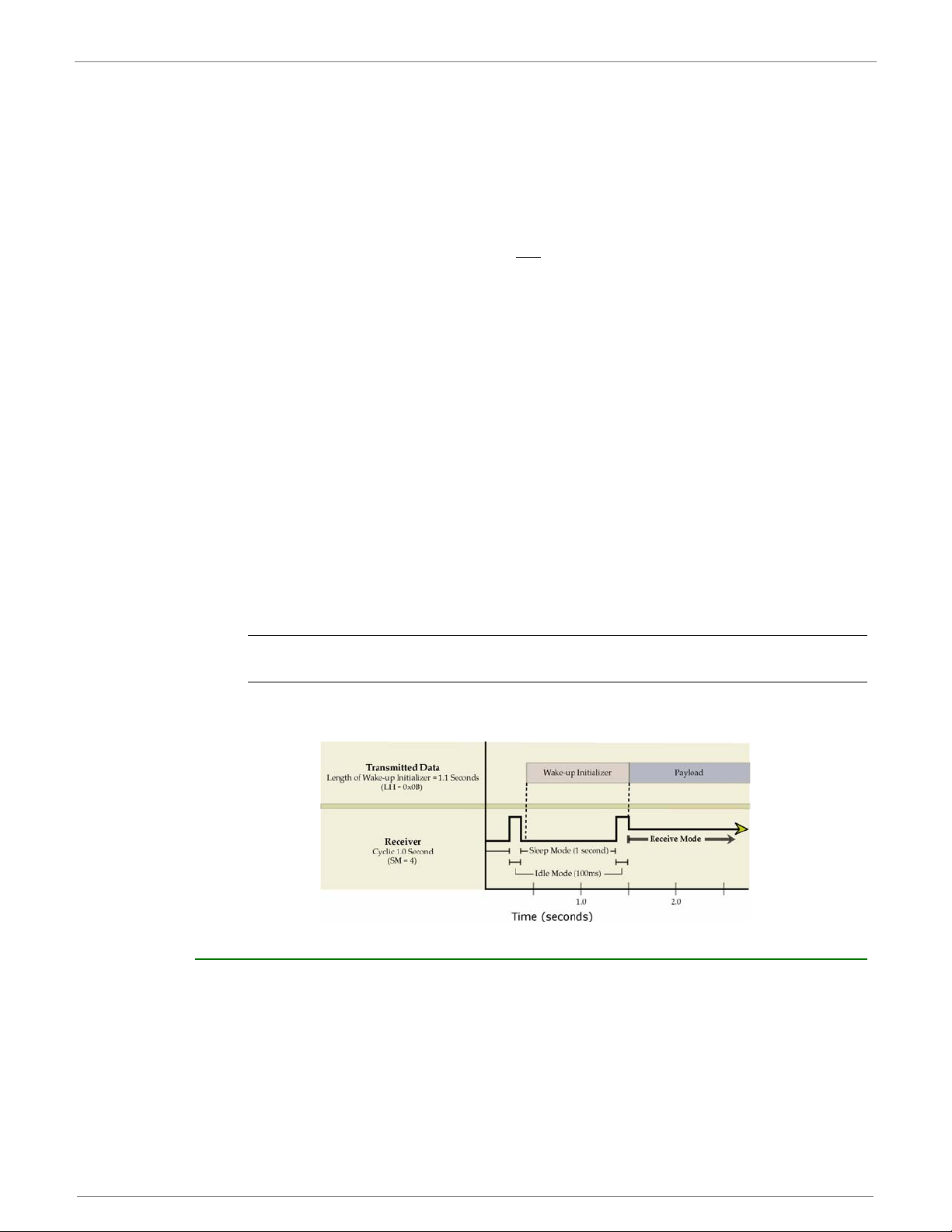
The cyclic interval time defined by the SM (Sleep Mode) command must be shorter than the interval
time defined by LH (Wake-up Initializer Timer) command.
Figure 2-08. Correct Couration (LH > SM):
The length of the wake-up initializer exceeds the time interval of Cyclic Sleep. The receiver is
guaranteed to detect the wake-up initializer and receive the accompanying payload data.
Command Mode
To modify or read module parameters, the module must first enter into Command Mode (state in
which incoming characters are interpreted as commands). Two command types are supported:
AT Commands
Binary Commands
For modified parameter values to persist in the module registry, changes must be saved to nonvolatile memory using the WR (Write) command. Otherwise, parameters are restored to previously
saved values when the module is powered off and then on again.
© 2010 Digi Internatonal, Inc. 16
Page 17
9XTend™ OEM RF Module - Product Manual v2.x6x
AT Command Mode
To Enter AT Command Mode:
1. Send the 3-character command sequence "+++" and observe guard times before and after
the command characters. [refer to ‘Default AT Command Mode Sequence’ below.] The ‘Terminal’ tab (or other serial communications software) of the X-CTU Software can be used to
enter the sequence.
[OR]
2. Assert (low) the CONFIG
pulse the SHDN
[If the module is mounted to a Digi RS-232/485 Interface Board, the result can be achieved
by pressing the configuration switch down for 2 seconds.]
Default AT Command Mode Sequence (for transition to Command Mode):
No characters sent for one second [refer to the BT (Guard Time Before) Command]
Input three plus characters (“+++”) within one second
[refer to the CC (Command Sequence Character) Command.]
No characters sent for one second [refer to the AT (Guard Time After) Command.]
All of the parameter values in the sequence can be modified to reflect user preferences.
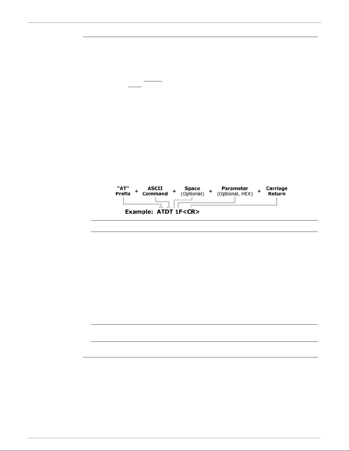
To Send AT Commands:
Send AT commands and parameters using the syntax shown below.
Figure 2-09. Syntax for sending AT Commands
pin and turn the power going to the module off and back on (or
pin).
To read a parameter value stored in the module register, leave the parameter field blank.
The preceding example would change the module’s Destination Address to "0x1F". To store the
new value to non-volatile (long term) memory, the Write (ATWR) command must subsequently be
sent before powering off the module.
System Response. When a command is sent to the module, the module will parse and execute
the command. Upon successful execution of a command, the module returns an “OK” message. If
execution of a command results in an error
To Exit AT Command Mode:
1. If no valid AT Commands are received within the time specified by CT (Command Mode
Timeout) Command, the module automatically returns to Idle Mode.
[OR]
2. Send ATCN (Exit Command Mode) Command.
For an example of programming the RF module using AT Commands and descriptions of each configurable parameter, refer to the "RF Module Configuration" chapter [p19].
Binary Command Mode
Sending and receiving parameter values using binary commands is the fastest way to change
operating parameters of the module. Binary commands are used most often to sample signal
strength [refer to DB (Received Signal Strength) parameter] and/or error counts; or to change
module addresses and channels for polling systems when a quick response is necessary. Since the
sending and receiving of parameter values takes place through the same serial data path as 'live'
data (received RF payload), interference between the two types of data can be a concern.
Common questions about us
What are the implications of asserting CMD while live data is being sent or received?
ing binary commands:
, the module returns an “ERROR” message.
© 2010 Digi Internatonal, Inc. 17
Page 18
9XTend™ OEM RF Module - Product Manual v2.x6x
After sending serial data, is there a minimum time delay before CMD can be asserted?
Is a time delay required after CMD is de-asserted before payload data can be sent?
How does one discern between live data and data received in response to a command?
The CMD pin (pin 10) must be asserted in order to send binary commands to the module. The
CMD pin can be asserted to recognize binary commands anytime during the transmission or reception of data. The status of the CMD signal is only checked at the end of the stop bit as the byte is
shifted into the serial port. The application does not allow control over when data is received,
except by waiting
If the command is sent in the middle of a stream of payload data to be transmitted, the command
will essentially be executed in the order it is received. If the module is continuously receiving data,
the radio will wait for a break in the received data before executing the command. The CTS
will frame the response coming from the binary command request [refer to figure below].
A minimum time delay of 100 μs (after the stop bit of the command byte has been sent) must be
observed before the CMD pin can be de-asserted. The command executes after all parameters
associated with the command have been sent. If all parameters are not received within 0.5 seconds, the module returns to Idle Mode.
Note: When parameters are sent, they are two bytes long with the least significant byte sent first.
Binary commands that return one parameter byte must be written with
Commands can be queried for their current value by sending the command logically ORed (bitwise) with the value 0x80 (hexadecimal) with CMD asserted. When the binary value is sent (with
no parameters), the current value of the command parameter is sent back through the DO pin.
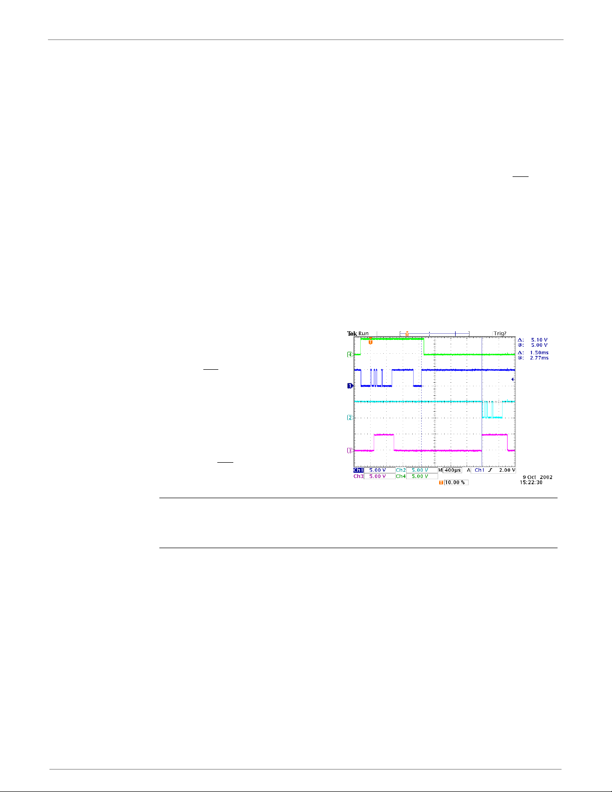
Figure 2-010.Binary Command Write then Read
Signal #4 is CMD
Signal #1 is the DI signal
Signal #2 is the DO signal from the radio
Signal #3 is CTS
for dead time between bursts of communication.
signal
two parameter bytes.
In this graph, a value was written to a register and then read out to verify it. While
not in the middle of other received data,
note that the CTS
response out of the module.
IMPORTANT: In order for the module to recognize a binary command, the RT (GPI1 Configuration)
parameter must be set to one. If binary programming is not enabled (RT parameter value is not equal
to ‘1’), the module will not recognize that the CMD pin is asserted and therefore will not recognize the
data as binary commands.
Refer to [p19] for a binary programming example (DT command example returns two bytes).
signal outlines the data
© 2010 Digi Internatonal, Inc. 18
Page 19

3. RF Module
Programming Examples
Refer to the ‘Command Mode’ section [p17] for information regarding entrance into Command
Mode, sending AT commands and exiting Command Mode. Refer to the ‘X-CTU’ section [p81] of
the ‘Development Guide’ for more information regarding MaxStream’s configuration software.
AT Commands
To Send AT Commands (Using the ‘Terminal’ tab of the X-CTU Software)
Example: Utilize the 'Terminal' tab of the X-CTU Software to change the module's DT (Destination Address) parameter and save the new address to non-volatile memory. This example
Note: Do not send commands to the module
during sh programming (when parameters
being wrien to the
are
module registry).
Wait for the "OK" system response that follows the ATWR
command before entering the next command
or use ow control.
requires the installation of Digi’s X-CTU Software and a serial connection to a PC.
Select the ‘Terminal’ tab of the X-CTU Software and enter the following command lines:
Method 1 (One line per command)
Send AT Command
+++
ATDT <Enter>
ATDT1A0D <Enter>
ATWR < Enter>
ATCN <Enter>
Method 2 (Multiple commands on one line)
Send AT Command
+++
ATDT <Enter>
ATDT1A0D,WR,CN <Enter>
System Response
OK <CR> (En
{current value} <CR> (Read Destination Address)
OK <CR> (Modify Destination Address)
OK <CR> (Write to non-volatile memory)
OK <CR> (Exit Command Mode)
System Response
OK <CR> (Enter into Command Mode)
{current value} <CR> (Read Destination Address)
OK <CR> (Execute commands)
ter into Command Mode)
Note: When using X-CTU Software to program a module, PC com port settings must match the baud
(interface data rate), parity & stop bits parameter settings of the module. Use the 'Com Port Setup'
section of the “PC Settings” tab to configure PC com port settings to match those of the module.
Binary Commands
To Send Binary Commands:
Example: Use binary commands to change the RF module's destination address to 0x1A0D and
save the new address to non-volatile memory.
1. RT Command must be set to '1'
2. Assert CMD (Pin 10 is driven high). (Enter Binary Command Mode)
3. Send Bytes [parameter bytes must be 2 bytes long]:
4. De-assert CMD (pin 10 is driven low). (Exit Binary Command Mode)
Note: CTS (pin 9) is high when a command is being executed. Hardware flow control must be disabled
as CTS will hold off parameter bytes.
© 2010 Digi International Inc. 19
in AT Command Mode to enable binary programming.
)dnammoC )sserddA noitanitseD( TD dneS(00
)se
tyb retemarap fo etyb tnacifingis tsaeL(D0
)setyb retemarap fo etyb tnacifingis tsoM(A1
rW( RW dneS(80
)dnammoC )eti
Page 20

9XTend™ OEM RF Module - Product Manual v2.x6x
Command Reference Table
Table 3-01. XTend Commands (The RF modules expect numerical values in hexadecimal. Hexadecimal values are designated by a “0x”
AT
Command
%V 0x3B (59d) Board Voltage 0x2CCCA - 0x5BFFA [read-only] Diagnostics 4 --
AT 0x05 (5d) Guard Time After 2 - (ATST-3) [x 100 msec] Command Mode Options 2 0x0A (10d)
BD 0x15 (21d) Interface Data Rate
BT 0x04 (4d) Guard Time Before 0 - 0xFFFF [x 100 msec] Command Mode Options 2 0x0A (
CT 0x06 (6d) Command Mode Timeout 2 - 0xFFFF [x 100 ms] Command Mode Options 2 0xC8 (200d)
DB 0x36 (54d) Received Signal Strength 0x6E - 0x28 [read-only] Diagnostics 2
FS 0x3E (62d) Forced Sync Time 0 - 0xFFFF [x 10 msec] RF Interfacing 2 0
FT 0x24 (36d) Flow Control Threshold 0
HT 0x03 (3d) Time before Wake-up Initializer 0 - 0xFFFF [x 100 msec] Sleep (Low Power) 2
HV -- Hardware Version 0 - 0xFFFF [read-only] Diagnostics 2 --
ID 0x27 (39d) Modem VID
KY 0x3C (60d) AES Encryption Key 0 - (64 hex digits
LH 0x0C (12d) Wake-up Initializer Timer 0 - 0xFF [x 100 msec] Sleep (Low Power) 1 1
MT 0x3D (61d) Multi-Transmit 0 01ytiruceS & gnikrowteNFFx0 -
MY 0x2A (42d) Source Address 0 2ytiruceS & gnikrowteNFFFFx0 -
PD v2.x20* 0x47 (71d) Minimum Polling Delay
prex. Decimal equivalents are designated by a “d” sux.)
Binary
Command
x0TD
D0x0HF
0BN
AT Command Name Parameter Range
0 - 8 (standard rates)
0x39 - 0x1C9C38 (non-standard rates)
carahC ecneuqeS dnammoC)d91( 31x0CC
- (DI buffer size - 0x11) [Bytes] Serial Interfacing 2
G evieceR)d61( 01x0DG
0x11 - 0x7FFF (user-settable)
0x8000 - 0xFFFF (factory-set, read-only)
A nigeB gnilloP)d96( 54x0*02x.2v BP
0 - 0xFFFF
(Base: (x 1 ms), Remote: [x 10 ms])
Command
Category
Serial Interfacing 4 3
doM dnammoC2 - 0esaB rebmuN--FC
ireS4 - 0noitarugifnoC 1OPG)d13( F1x0SC
songaiDFFFFx0 - 0tnuoC rorrE evieceR)d51( F0x0RE
Networking & Security 2
all set to 'F') Networking & Security 2 0 (disabled)
gnikrowteN6 - 0edoM FR)d94( 13x0*02x.2v DM
Networking & Security 2 0
wteNFFFFx0 - 0sserddA dnE gnilloP)d07( 64x0*02x.2v EP
# Bytes
Returned
2ytiruceS & gnikrowteNFFFFx0 - 0ksaM sserddA)d81( 21x0KM
Factory
Default
----ytiruceS & gnikrowteN--YM tes-otuA)d46( 04x0MA
01gnicafretnI laireS2 - 0elbanE IPA--*02x.2v PA
11gnicafretnI FR1 - 0etaR ataD FR)d75( 93x0RB
10d)
21gnicafretnI laireS4 - 0noitarugifnoC 2OPG)d04( 82x0DC
11snoitpO e
----snoitpO edoM dnammoC--edoM dnammoC tixE)d9( 90x0NC
01gnicafretnI la
--
02ytiruceS & gnikrowteNFFFFx0 - 0sserddA noitanitseD)d0( 00
----snoitpO edoM dnammoC--ffO ohcE)d01( A0x00E
----snoitpO edoM dnammoC--nO ohcE)d11( B0x01E
02scit
----)rewoP woL( peelS--rezilaitinI pu-ekaW ecroF)d31(
01gnicafretnI laireS1 - 0lortnoC wolF erawtfoS)d7( 70x0LF
DI buffer size
minus 0x11
02scitsongaiDFFFFx0 - 0tnuoC doo
01ytiruceS & gnikrowteN9 - 0lennahC gnippoH)d71( 11x0PH
0xFFFF
(65535d)
0x3332
(13106d)
01ytiruceS &
0xFFFF
(65535d)
0xFFFF
(65535d)
01gnicafretnI laireS4 - 0ytiraP)d53( 32x
02ytiruceS & gnikrowteNFFFFx0 - 0sserdd
02ytiruceS & gnikro
)d34( ]"+"[ B2x01snoitpO edoM dnammoCF7x0 - 02x0ret
© 2010 Digi Internatonal, Inc. 20
Page 21

9XTend™ OEM RF Module - Product Manual v2.x6x
Table 3-01. XTend Commands (The RF modules expect numerical values in hexadecimal. Hexadecimal values are designated by a “0x”
AT
Command
PK 0x29 (41d) Maximum RF Packet Size 1 - 0x800 [Bytes] RF Interfacing 2 varies
RB 0x20 (32d) Packetization Threshold 1 - Current value of PK Serial Interfacing 2 0x800 (2048d)
RC -- Ambient Power - Single Channel 0 - 0x31 [dBm, read-only] Diagnostics 1 --
RM -- Ambient Power - All Channels No parameter - 0x7D0 Diagnostics
RO 0x21 (33d) Packetization Timeout 0 - 0xFFFF [x UART character time] Serial Interfacing 2 3
RP 0x22 (34d) RSSI PWM Timer 0 - 0xFF [x 100 msec] Diagnostics 1 0x20 (32d)
SH 0x25 (37d) Serial Number High 0 - 0xFFFF [read-only] Diagnostics 2 varies
SL 0x26 (38d) Serial Number
SM 0x01 (1d) Sleep Mode 0 - 8 (3 is reserved) Sleep (Low Power) 1 0
ST 0x02 (2d) Time before Sleep (ATAT+3) - 0x7FFF [x 100 msec] Sleep (Low Power) 2 0x64 (100d)
TP 0x38 (56d) Board Temperature 0 - 0x7F [read-only] Diagnostics 1 --
TR 0x1B (27d) Delivery Failure Count 0 - 0xFFFF [read-only] Diagnostics 2 0
TT 0x1A (26d) Streaming Limit 0 - 0xFFFF [0 = disabled] Networking & Security 2 0
VR 0x14 (20d) Firmware Version 0 - 0xFFFF
prex. Decimal equivalents are designated
Binary
Command
x0WP
AT Command Name Parameter Range
D)d52( 91x0NR
noitarugifnoC 1IPG)d22( 61x0TR
Low 0 - 0xFFFF [read-only] Diagnostics 2 varies
by a “d” sux.)
- 0ylnO timsnarT)d36( F3x0XT
[read-only] Diagnostics 2 --
Command
Category
gaiDgnirts snruteRsrebmuN gninraW evitcA--AW
(--etirW)d8( 80x0RW
# Bytes
Returned
2--
Factory
Default
)ttaW 1( 41gnicafretnI FR4 - 0leveL rewoP XT)d85( A3x0LP
01)rewoP woL( peelS1 - 0pu-ekaW niP)d92( D1
----)laicepS(--stluafeD erotseR)d41( E0x0ER
01ytiruceS & gnikrowteN]stols[ FFx0 - 0stolS yale
01gnicafretnI laireS2 - 0
01gnicafretnI laireS1 - 0stiB potS)d55( 73x0BS
01gnicafretnI FR1
----scitsongaiDgnirts snruteResobrev - noisreV erawmriF--LV
----scitson
----scitsongaiDgnirts snruteRataD gninraW--NW
----)laicepS
----scitsongaiDgnirts snruteRsrebmuN gninraW ykcitS--SW
)d01( A0x01ytiruceS & gnikrowteNFFx0 - 0seirteR)d42( 81x0 RR
* Firmware version in which command and parameter options were rst supported
© 2010 Digi Internatonal, Inc. 21
Page 22

9XTend™ OEM RF Module - Product Manual v2.x6x
Command Descriptions
Commands in this section are listed alphabetically. Command categories are designated between
the "< >" symbols that follow each command title. By default, XTend RF Modules expect numerical
values in hexadecimal since the default value of the CF (Number Base) Parameter is '1'. Hexadecimal values are designated by the "0x" prefix and decimal values by the "d" suffix.
%V (Board Voltage) Command
<Diagnostics> %V Command is used to read the
current voltage of the module circuit board.
Sample Output:
5.02 V (when ATCF = 0)
5051F (when ATCF = 1) *
5.02 (when ATCF = 2)
* When CF = 1 (default), a hex integer is shown
that is equal to (voltage * 65536d).
AM (Auto-set MY) Command
<Networking & Security> AM Command is used
to automatically set the MY (Source Address)
parameter from the factory-set serial number of
the module. The address is formed with bits 29,
28 and 13-0 of the serial number (in that order).
The resulting value is displayed as a result of this command.
AP (API Enable) Command
<Serial Interfacing> The AP command is used to
enable the module to operate using the framebased API operation.
AT (Guard Time After) Command
AT Command: AT%V
Binary Command:
Parameter Range (read-only):
Number of bytes returned: 4
AT Command: ATAM
Binary Command: 0x40 (64 decimal)
AT Command: ATAP
Parameter Range:0 - 2
Default Parameter Value:0
Number of Bytes Returned:1
Minimum Firmware Version Required: 2.x20
0x3B (59 decimal)
0x2CCCA - 0x5BFFA
(2.80 - 5.75 decimal)
Parameter Configuration
0
1
2
API Disabled
(Transparent Operation)
API enabled
(w/out escaped
characters)
API enabled
(with escaped
characters)
<Command Mode Options> AT Command is used
to set/read the time-of-silence that follows the
command sequence character (CC Command) of
the AT Command Mode Sequence (BT + CC +
AT). By default, 1 second must elapse before and
after the command sequence character.
The times-of-silence surrounding the command
sequence character are used to prevent inadvertent entrance into AT Command Mode.
Refer to the ‘AT Command Mode’ section [p17] for
more information regarding the AT Command Mode Sequence.
AT Command: ATAT
Binary Command: 0x05 (5 decimal)
Parameter Range:2 - (ATST-3), up to 0x7FFC
[x 100 milliseconds]
Default Parameter Value: 0x0A (10 decimal)
Number of bytes returned: 2
Related Commands: BT (Guard Time Before),
CC (Command Sequence Character)
© 2010 Digi Internatonal, Inc. 22
Page 23
9XTend™ OEM RF Module - Product Manual v2.x6x
BD (Interface Data Rate) Command
<Serial Interfacing> The BD command is used to
set and read the serial interface data rate (baud
rate) used between the RF module and host. This
parameter determines the rate at which serial
data is sent to the module from the host. Modified
interface data rates do not take effect until the CN
(Exit AT Command Mode) command is issued and
the system returns the 'OK' response.
When parameters 0-8 are sent to the module, the
respective interface data rates are used (as
shown in the table on the right).
The RF data ra
eter. If the interface data rate is set higher than
the RF data rate, a flow control configuration may
need to be implemented.
The range between standard and non-standard
baud rates (0x09 - 0x38) is invalid.
Non-standard Interface Data Rates:
Any value above 0x38 will be interpreted as an
actual baud rate. When a value above 0x38 is
sent, the closest interface data rate represented
by the number is stored in the BD register. For example, a rate of 19200 bps can be set by sending the following command line "ATBD4B00". NOT
dard interface data rates can only be set and read using the X-CTU ‘Terminal’ tab. Non-standard
rates are not accessible through the ‘Modem Configuration’ tab.
When the BD command is sent with a non-standard interface data rate, the UART will adjust to
accommodate the requested interface rate. In most cases, the clock resolution will cause the
stored BD parameter to vary from the parameter that was sent (refer to the table below). Reading
the BD command (send "ATBD" command without an associated parameter value) will return the
value actually stored in the module’s BD register
Parameters Sent Versus Parameters Stored
BD Parameter Sent (HEX) Interface Data Rate (bps) BD Parameter Stored (HEX)
te is not affected by the BD param-
AT Command: ATBD
Binary Command: 0x15 (21 decimal)
Parameter Ranges: 0 - 8 (standard rates)
0x39 - 0x1C9C38 (non-standard rates)
Parameter Configuration (bps)
01200
12400
24800
39600
419200
538400
657600
7 115200
8 230400
Default Parameter Value: 3
Non-standard baud rates supported as of
firmware v2.x20
Number of bytes returned: 4
E: When using Digi’s X-CTU Software, non-stan-
.
000210
4002,914
7002,5117
B21003C21
702B1002,511002C1
BR (RF Data Rate) Command
<RF Interfacing> The BR command is used to set
and read the RF data rate (rate that RF data is
transmitted over-the-air) of the module.
AT Command: ATBR
Binary Command: 0x39 (57 decimal)
Parameter Range:0 - 1
Parameter
09600
1 115200
Default Parameter Value:1
Number of bytes returned: 1
Baud (bps)
Configuration
© 2010 Digi Internatonal, Inc. 23
Page 24

9XTend™ OEM RF Module - Product Manual v2.x6x
BT (Guard Time Before) Command
<AT Command Mode Options> The CC command
is used to set/read the ASCII character used
between guard times of the AT Command Mode
Sequence (BT + CC + AT). This sequence enters
the module into AT Command Mode so that data
entering the module (from the host) is recognized
as commands instead of payload.
Refer to the ‘AT Command Mode’ section [p17] for
more information regarding the AT Command
Mode Sequence.
CC (Command Sequence Character) Command
<AT Command Mode Options> The CC command
is used to set/read the ASCII character used
between guard times of the AT Command Mode
Sequence (BT + CC + AT). This sequence enters
the module into AT Command Mode so that data
entering the module (from the host) is recognized
as commands instead of payload.
Refer to the ‘AT Command Mode’ section [p17] for
more information regarding the AT Command
Mode Sequence.
CD (GPO2 Configuration) Command
AT Command: ATCC
Binary Command: 0x13 (19 decimal)
Parameter Range: 0x20 - 0x7F
Default Parameter Value: 0x2B (ASCII “+”)
Number of bytes returned: 1
Related Commands: AT (Guard Time After), BT
(Guard Time Before)
AT Command: ATCC
Binary Command: 0x13 (19 decimal)
Parameter Range: 0x20 - 0x7F
Default Parameter Value: 0x2B (ASCII “+”)
Number of bytes returned: 1
Related Commands: AT (Guard Time After), BT
(Guard Time Before)
<Serial Interfacing> CD Command is used to
select/read the behavior of the GPO2 line (pin 3).
CF (Number Base) Command
<Command Mode Options> CF command is used
to set/read the command formatting setting.
The following commands are always entered and
read in hex, no matter the CF setting:
VR (Firmware Version)
HV (Hardware Version)
KY (AES Encryption Key)
AT Command: ATCD
Binary Command: 0x28 (40 decimal)
Parameter Range: 0 - 8 (standard rates)
Parameter Configuration
0 RX LED
1 Default High
2 Default Low
3 (reserved)
4
Default Parameter Value: 2
Number of bytes returned: 1
AT Command: ATCF
Parameter Range: 0 – 2
Parameter Configuration
Commands utilize default
0
1
2
Default Parameter Value: 1
Number of bytes returned: 1
number base; decimal
commands may output units
All commands forced to
unsigned, unit-less hex
Commands utilize their
default number base; no
units are output
RX LED
(valid address only)
© 2010 Digi Internatonal, Inc. 24
Page 25

9XTend™ OEM RF Module - Product Manual v2.x6x
CN (Exit AT Command Mode) Command
<Command Mode Options> The CN command is
used to explicitly exit the module from AT Command Mode.
CS (GPO1 Configuration) Command
<Serial Interfacing> CS Command is used to
select the behavior of the GP01 pin (pin 9). This
output can provide RS-232 flow control, control
the TX enable signal (for RS-485 or RS-422 operations).
By default, GP01 provides RS-232 CTS
Send) flow control.
CT (Command Mode Timeout) Command
<Command Mode Options> The CT command is
used to set and read the amount of inactive time
that elapses before the module automatically
exits from AT Command Mode and returns to Idle
Mode.
Use the CN (Exit AT Command Mode) command
to exit AT Command Mode manually.
DB (Received Signal Strength) Command
(Clear-to-
AT Command: ATCN
Binary Command: 0x09 (9 decimal)
AT Command: ATCS
Binary Command: 0x1F (31 decimal)
Parameter Range: 0 - 4
Parameter Configuration
0 RS-232 CTS
1 RS-485 TX enable low
2High
3 RS-485 TX enable high
4Low
Default Parameter Value: 0
Number of bytes returned: 1
Related Commands: RT (GPI1 Configuration),
TO (GP01 Timeout)
AT Command: ATCT
Binary Command: 0x06 (6 decimal)
Parameter Range:2 - 0xFFFF
[x 100 milliseconds]
Default Parameter Value: 0xC8 (200d)
Number of bytes returned: 2
Related Command: CN (Exit AT Command
Mode)
flow control
<Diagnostics> DB Command is used to read the
receive signal strength (in decibels relative to milliWatts) of the last received packet. This parameter is useful in determining range characteristics
of the RF modules under various conditions.
In default mode, this command shows the power
level in signed decimal format with the units (dBm). If CF = 1, the magnitude of the value is presented in unsigned hex. If CF = 2, the value is presented in decimal, but without the units.
Sample Output:-88 dBm(
58 (when ATCF = 1)
-88 (when ATCF = 2)
NOTE: If the DB register is read before the module has received an RF packet, the module will
return a value of 0x8000 (which means an RF packet has not yet been received).
when ATCF = 0)
AT Command: ATDB
Binary Command: 0x36 (54 decimal)
Parameter Range (read-only): 0x6E - 0x28
(-110 to -40 Decimal)
Number of bytes returned: 2
© 2010 Digi Internatonal, Inc. 25
Page 26

9XTend™ OEM RF Module - Product Manual v2.x6x
DT (Destination Address) Command
<Networking & Security> DT Command is used to
set/read the networking address of an RF module.
The modules utilize three filtration layers: Vendor
ID Number (ATID), Channel (ATHP), and Destination Address (ATDT). The DT command assigns an
address to a radio that enables it to communicate
with other radios in the network. The simplest use
of this command is that when MY=0xFFFF and
MK=0xFFFF on all radios in a network, only radios
with matching DT's will communicate with each
ther.
o
If MY is not 0xFFFF, then DT acts as a transmit address and MY acts as a receive address. For
example, MY can be set to unique values 1, 2, 3, etc. on unique radios in the network. Then set DT
on the transmitting radio to match the MY of the receiving radio you intend to communicate with.
Setting DT=0xFFFF will broadcast to all radios in the network. Refer to the 'Addressing' section
[p45] for more information.
E0 (Echo Off) Command
<Command Mode Options> E0 Command turns
off character echo in AT Command Mode.
By default, echo is off.
E1 (Echo On) Command
<Command Mode Options> E1 Command enables
character echo in AT Command Mode. Each typed
character will be echoed back to the terminal
when ATE1 is active. E0 (Echo Off) is the default.
AT Command: ATDT
Binary Command: 0x00
Parameter Range:0 - 0xFFFF
Default Parameter Value: 0
Number of bytes returned: 2
Related Commands: HP (Hopping Channel), ID
(Modem VID), MK (Address Mask), MY (Source
Address)
AT Command: ATE0
Binary Command: 0x0A (10 decimal)
AT Command: ATE1
Binary Command: 0x0B (11 decimal)
ER (Receive Error Count) Command
<Diagnostics> The ER command is used to set/
read the number of receive-errors. The error
count records the number of packets partially
received then aborted on a reception error. This
value returns to 0 after a reset and is not nonvolatile (Value does not persist in the module's
memory after a power-up sequence). Once the
Receive Error Count reaches its maximum value
(up to 0xFFFF), it remains at its maximum count
value until the maximum count value is explicitly changed or the module is reset.
The ER parameter is not reset by pin,
FH (Force Wake-up Initializer) Command
<Sleep (Low Power)> The FH command is used
to force a Wake-up Initializer to be sent on the
next transmission. Use only with cyclic sleep
modes active on remote modules.
ATFH will not send a long header if ATHT = 0xFFFF. WR (Write) Command does not need to be
issued with FH Command.
serial port or cyclic sleep modes.
AT Command: ATER
Binary Command: 0x0F (15 decimal)
Parameter Range: 0 - 0xFFFF
Default Parameter Value: 0
Number of bytes returned: 2
Related Commands: GD (Receive Good Count)
AT Command: ATFH
Binary Command: 0x0D (13 decimal)
© 2010 Digi Internatonal, Inc. 26
Page 27

9XTend™ OEM RF Module - Product Manual v2.x6x
FL (Software Flow Control) Command
<Serial Interfacing> The FL command is used to
configure software flow control. Hardware flow
control is implemented with the module as the
GP01 pin (CTS
regulates when serial data can be transferred to
the module.
FL Command can be used to allow software flow
control to also be enabled. The XON character
used is 0x11 (17 decimal). The XOFF character
used is 0x13 (19 decimal)
FS (Forced Synch Time) Command
<RF Interfacing> The FS command only applies
to streaming data. Normally, only the first packet
of a continuous stream contains the full RF initializer. The RF modules then remain synchronized
for subsequent packets of the stream. This
parameter can be used to periodically force an RF
initializer during such streaming. Any break in
UART character reception long enough to drain
the DI Buffer (UART receive buffer) and cause a pause in RF data transmission will also cause an
RF initializer to be inserted on the next transmission.
FT (Flow Control Threshold) Command
pin of the OEM RF module), which
AT Command: ATFL
Binary Command: 0x07 (7 decimal)
Parameter Range: 0 - 1
Parameter Configuration
0
1
Default Parameter Value: 0
Number of bytes returned: 1
AT Command: ATFS
Binary Command: 0x3E (62 decimal)
Parameter Range:0 - 0xFFFF
[x 10 milliseconds]
Default Parameter Value: 0
Number of bytes returned: 2
Disable software
flow control
Enable software
flow control
<Serial Interfacing> The FT command is used to
set/read the flow control threshold. When FT
bytes have accumulated in the DI buffer (UART
Receive), CTS
ware flow control character is transmitted.
GD (Receive Good Count) Command
<Diagnostics> The GD command is used to set/
read the count of good received RF packets. Its
parameter value is reset to 0 after every reset
and is not non-volatile (The parameter value does
not persist in the RF module's memory after a
power-up sequence). Once the "Receive Good
Count" reaches its maximum value (up to
0xFFFF), it remains at its maximum count value
until the maximum count value is manually
changed or the module is reset.
The GD parameter is not reset by pin, serial port or cycli
is de-asserted or the XOFF soft-
AT Command: ATFT
Binary Command: 0x24 (36 decimal)
Parameter Range:
0 - (DI buffer size minus 0x11) [Bytes]
Default Parameter Value: DI Buffer size minus
0x11 (17 decimal)
Number of bytes returned: 2
AT Command: ATGD
Binary Command: 0x10 (16 decimal)
Parameter Range: 0 - 0xFFFF
Default Parameter Value: 0
Number of bytes returned: 2
Related Commands: ER (Receive Error Count)
c sleep modes.
© 2010 Digi Internatonal, Inc. 27
Page 28

9XTend™ OEM RF Module - Product Manual v2.x6x
HP (Hopping Channel) Command
<Networking & Security> The HP command is
used to set/read the RF module's hopping channel
number. A channel is one of three layers of filtration available to the module.
In order for modules to communicate with each
other, the modules must have the same channel
number since each channel uses a different hopping sequence. Different channels can be used to
prevent modules in one network from listening to
transmissions of another.
HT (Time before Wake-up Initializer) Command
<Sleep (Low Power)> The HT command is used
to set/read the time of inactivity (no serial or RF
data is sent or received) before a wake-up initializer is sent by a TX (transmitting) RF module. The
HT parameter should be set shorter than inactivity timeout [ST Command] time of any RX
(receiving) modules operating in Cyclic Sleep
(SM=4-8). The wake-up initializer sent by the TX
module instructs all RX modules to remain awake
to receive RF data.
From the RX module perspective: After HT time
elapses and
is met, the RX module goes into cyclic sleep. In cyclic sleep, the RX module wakes once per sleep
interval [SM Command] to check for a wake-up initializer. When a wake-up initializer is detected,
the module stays awake to receive data. The wake-up initializer must be longer than the cyclic
sleep interval to ensure that sleeping modules detect incoming data.
When HT time elapses, the TX module knows it needs to send a wake-up Initializer for all RX modules to remai
the inactivity timeout [ST Command]
n awake and receive the next transmission.
AT Command: ATHP
Binary Command: 0x11 (17 decimal)
Parameter Range: 0 - 9
Default Parameter Value: 0
Number of bytes returned: 1
Related Commands: ID (Modem VID), DT
(Destination Address), MK (Address Mask)
AT Command: ATHT
Binary Command: 0x03 (3 decimal)
Parameter Range:0 - 0xFFFF
[x 100 milliseconds]
Default Parameter Value: 0xFFFF (wake-up
initializer will not be sent)
Number of bytes returned: 2
Related Commands: LH (Wake-up Initializer
Timer), SM (Sleep Mode), ST (Time before
Sleep)
HV (Hardware Version) Command
<Diagnostics> The HV command is used to read
the hardware version of the RF module.
ID (Modem VID) Command
<Networking & Security> The ID command is
used to set/read the VID (Vendor Identification
Number) of the RF module. RF modules must
have matching VIDs in order to communicate.
AT Command: ATHV
Parameter Range:0 - 0xFFFF [Read-only]
Minimum Firmware Version Required: v1.x80
AT Command: ATID
Binary Command: 0x27 (39 decimal)
Parameter Range:
0x11 - 0x7FFF (user-settable)
0 - 0x10 & 0x8000 - 0xFFFF (factory-set)
Default Parameter Value: 0x3332 (13106d)
Number of bytes returned: 2
© 2010 Digi Internatonal, Inc. 28
Page 29

9XTend™ OEM RF Module - Product Manual v2.x6x
KY (AES Encryption Key) Command
<Networking & Security> The KY command is
used to set the 256-bit AES (Advanced Encryption
Standard) key for encrypting/decrypting data.
Once set, the key cannot be read out of the module by any means. The entire payload of the
packet is encrypted using the key and the CRC is
computed across the ciphertext. When encryption
is enabled, each packet carries an additional 16
bytes to convey the random CBC Initialization
Vector (IV) to the receiver(s). The KY value may
be “0” or any 256-bit value (= 64 hex digits =
by itself with no parameters, causes an error.
A module with the wrong key (or no key) will receive encrypted data, but the data driven out the
serial port will be meaningless. Likewise, a module with a key will receive unencrypted data sent
from a module without a key, but the output will be meaningless. Because CBC mode is utilized,
repetitive data appears differently in different transmissions due to the randomly-generated IV.
NOTE: For international (non-U.S.) variants of 9XTend modules, the encrypti
AES. The command operates the same except the key length is 16 bytes rather than 32 bytes.
This pertains to part numbers ending with -NA or -128 (the -NA and -128 suffix mean the same
thing), no matter what firmware version is loaded. This also pertains to the Australia version of
firmware 22xx, no matter what part number 9XTend it is loaded onto.
LH (Wake-up Initializer Timer) Command
<Sleep (Low Power)> The LH Command is used
to set/read the duration of time during which the
wake-up initializer is sent. When receiving modules are in Cyclic Sleep Mode, they power-down
after a period of inactivity (as specified by the ST
parameter) and will periodically wake and listen
for transmitted data. In order for the receiving
modules to remain awake, they must detect
~35ms of the wake-up initializer.
LH Command must be used whenever a receiving
module is operating in Cyclic Sleep Mode. The
Wake-up Initia
(Sleep Mode) parameter]. If the wake-up initializer time were less than the Cyclic Sleep interval,
the connection would be at risk of missing the wake-up initializer transmission.
Refer to figures loated under the SM command description to view diagrams of correct and incorrect configurations. The images emphasize that the LH value must be greater than the SM value.
lizer Time must be longer than the cyclic sleep time that [as determined by SM
AT Command: ATKY
Binary Command: 0x3C (60 decimal)
Parameter Range:
0 - (64 hex digits all set
Default Parameter Value: 0 (disabled)
Number of bytes returned: 2
Number Base: Always Hexadecimal
32 bytes). Any other value, including entering ATKY
AT Command: ATLH
Binary Command: 0x0C (12 decimal)
Parameter Range:0 - 0xFF
Default Parameter Value: 1
Number of bytes returned: 1
Related Commands: HT (Time before Wake-up
Initializer), SM (Sleep Mode), ST (Time before
Sleep)
to 'F')
on key is 128-bit
[x 100 milliseconds]
© 2010 Digi Internatonal, Inc. 29
Page 30

9XTend™ OEM RF Module - Product Manual v2.x6x
MD (RF Mode) Command
<Networking & Security> The MD command is
used to select/read the settings that enable the
Polling and Repeater Modes on the module.
Polling Mode - A ‘Polling Base’ is responsible for
polling remotes. A ‘Polling Remote’ requires a poll
in order to transmit.
Repeater Mode - A ‘Repeater’ re-sends RF data
unless the transmission is addressed to it or if the
transmission has already been detected. A
‘Repeater End Node’ handles repeated messages,
but will not repeat the message over-the-air.
Refer to the P
of the ‘RF Communication Modes’ chapter for
more information.
MK (Address Mask) Command
<Networking & Security> The MK command is
used to set/read the Address Mask of a module.
All RF data packets contain the Destination
Address of the TX (transmitting) module. When a
packet is received, the TX module Destination
Address is logically "ANDed" (bitwise) with the
Address Mask of the RX (receiving) module. The
resulting value must match the Destination
Address or Address Mask of the RX module for the
packet to be received and sent out the RX module's DO (Data Out) pin. If the "ANDed" value does not m
Mask of the RX module, the packet is discarded.
Sniffer Mode (when MK = 0): ACK requests are ignored and every RX (receive) frame is sent to
the UART, without regard for repeated frames.
All “0” values are treated as irrelevant values and ignored.
Refer to the ‘Addressing’ section [p45] for more information.
olling and Repeater Mode sections
AT Command: ATMD
Binary Command: 0x31 (49 decimal)
Parameter Range: 0 - 6
Parameter Configuration
0
1 [reserved - not used]
2
3Polling Base
4 Polling Remote
5 Repeater
6 Repeater End Node
Default Parameter Value: 0
Number of bytes returned: 1
Minimum Firmware Version Required: 2.x20
AT Command: ATMK
Binary Command: 0x12 (18 decimal)
Parameter Range:0 - 0xFFFF
Default Parameter Value: 0xFFFF (65535d)
Number of bytes returned: 2
Related Commands: DT (Destination Address),
HP (Hopping Channel), ID (Modem VID), MY
(Source Address)
atch the Destination Address or Address
Transparent Operation
(Repeate
[reserved - not used]
r Base)
MT (Multi-transmit) Command
<Networking & Security> The MT command is
used to enabled multiple transmissions of RF data
packets. When Multi-transmit Mode is enabled
(MT > 0), packets do not request an ACK
(acknowledgement) from the receiving RF module(s). MT takes precedence over RR, so if both
MT and RR are non-zero, then MT+1 packets will
be sent (with no ACK requests).
When a receiving module receives a packet with
remaining forced retransmissions, it calculates
the length of the packet and inhibits transmission
for the amount of time required for all retransmiss
slots are inserted between 0 and RN before transmission is allowed from the receiving module(s).
This prevents all listening modules from transmitting at once upon conclusion of a multiple transmission event (when RN > 0).
NOTE: The actual number of forced transmissions is the parameter value plus one. For example, if
MT = 1, two transmissions of each packet will be sent.
AT Command: ATMT
Binary Command: 0x3D (61 decimal)
Parameter Range: 0 - 0xFF
Default Parameter Value:0 (no forced
retransmissions)
Number of bytes returned: 1
Related Commands: Networking (DT, MK, MY,
RN, TT), Serial Interfacing (BR, PK, RB, RO), RF
Interfacing (FS)
ions. Thereafter, a random number of delay
© 2010 Digi Internatonal, Inc. 30
Page 31

9XTend™ OEM RF Module - Product Manual v2.x6x
Refer to the ‘Multi-transmit Mode’ section [p46] for more information.
MY (Source Address) Command
<Networking & Security> The MY command is
used to set/read the Source Address of the RF
module.
Refer to the DT command and the 'Addressing'
section [p45] for more information.
NB (Parity) Command
<Serial Interfacing> The NB command is used to
select/read the parity settings of the RF module
for UART communications.
PB (Polling Begin Address) Command
AT Command: ATMY
Binary Command: 0x2A (42 decimal)
Parameter Range: 0 - 0xFFFF
Default Parameter Value: 0xFFFF (Disabled -
DT (Destination Address) parameter serves as
both source and destination address.)
Number of bytes returned: 2
Related Commands: DT (Destination Address),
HP (Hopping Channel), ID (Modem VID), MK
(Address Mask)
AT Command: ATNB
Binary Command: 0x23 (35 decimal)
Parameter Range: 0 - 4
Parameter Configuration
0
18-bit even
2 8-bit odd
38-bit mark
4 8-bit space
Default Parameter Value: 0
Number of bytes returned: 1
8-bit (no parity or
7-bit (any parity)
<Networking & Security> PB command is used to
set/read the module’s Polling Begin Address - the
first address polled Polling Mode is enabled.
Polling Operations: The ‘Polling Base’ (MD = 3)
cycles through a sequential range of addresses,
polling each ‘Polling Remote’ (MD = 4). The base
then waits for a response & proceeds to the next
‘Polling Remote’. Each ‘Polling Remote’ responds
by sending the data from the Data In buffer following the RB & RO parameters. When there is no
eligible data to send, the ‘Polling Remote’ will not respond. The
address in the polling sequence after a short delay.
PD (Minimum Polling Delay) Command
<Networking & Security> The PD command is
used to set/read Polling Delay (Base, MD=3) or
Polling Timeout (Remote, MD=4).
Polling Delay (Base) is the time between polling
cycles. The Polling Base will start the polling cycle
after sending the first poll. After the polling cycle
has completed, the timer is restarted.
Polling Timeout (Remote) is the amount of time
the remote unit will hold data from the serial port
before discarding it. Data entered within the PD
time of the pol
l is transmitted and not discarded.
AT Command: ATPB
Binary Command: 0x45 (69 decimal)
Parameter Range: 0 - 0xFFFF
Default Parameter Value: 0
Number of bytes returned: 2
Minimum Firmware Version Required: 2.x20
Related Commands: MD (RF Mode), PE (Polling
End Address), PD (Minimum Polling Delay)
AT Command: ATPD
Binary Command: 0x47 (71 decimal)
Parameter Range: 0 - 0xFFFF
(Base: [x 1ms], Remote: [x 10ms])
Default Parameter Value: 0
Number of bytes returned: 2
Minimum Firmware Version Required: 2.x20
Related Commands: MD (RF Mode), PB (Polling
Begin Address), PE (Polling End Address)
‘Polling Base’ will move to the next
© 2010 Digi Internatonal, Inc. 31
Page 32

9XTend™ OEM RF Module - Product Manual v2.x6x
PE (Polling End Address) Command
<Networking & Security> PE command is used to
set/read the module’s Polling End Address - the
last address polled when Polling Mode is enabled.
Polling Operations: The ‘Polling Base’ (MD = 3)
cycles through a sequential range of addresses,
polling each ‘Polling Remote’ (MD = 4). The base
then waits for a response & proceeds to the next
‘Polling Remote’. Each ‘Polling Remote’ responds
by sending data from the DI buffer following the
RB & RO parameters. When there is no eligible
data to send, the ‘Polling Remote’ will not respond. The ‘Polling Base’ will move to the next
address in
PK (Maximum RF Packet Size) Command
<RF Interfacing> The PK command is used to set/
read the maximum size of RF packets transmitted
from an RF module. The maximum packet size
can be used along with the RB and RO parameters
to implicitly set the channel dwell time.
If PK is set above 256 and BR is subsequently
changed to 0, PK will automatically be lowered to
256 and a warning will be raised (refer to the BR
(RF Data Rate) and WN (Warning Data) commands for details).
Changes to the PK parameter may have a secondary effect on the RB (Packetization Threshold) parameter. RB must always be less than or equal to
PK. If PK is changed to a value that is less than the current value of RB, the RB value is automatically lowered to be equal to PK.
* When BR = 0 (9600 baud), the maximum PK value is 0x100 (256d). When BR = 1 (115,200
baud), the maximum PK value is 0x800 (2048d).
the polling sequence after a short delay.
AT Command: ATPE
Binary Command: 0x46 (70 decimal)
Parameter Range: 0 - 0xFFFF
Default Parameter Value: 0
Number of bytes returned: 2
Minimum Firmware Version Required: 2.x20
Related Commands: MD (RF Mode), PB (Polling
Begin Address), PD (Minimum Polling Delay)
AT Command: ATPK
Binary Command: 0x29 (41 decimal)
Parameter Range:1 - 0x800 [Bytes]
Default Parameter Value:0x100* or 0x800*
(256 or 2048 decimal)
Number of bytes returned: 2
Related Commands: BR (RF Data Rate) RB
(Packetization Threshold), RO (Packetization
Timeout), WN (Warning Data)
PL (TX Power Level) Command
<RF Interfacing> The PL command is used to set/
read the power level at which the RF module
transmits data
AT Command: ATPL
Binary Command: 0x3A (58 decimal)
Parameter Range: 0 - 4
Parameter Configuration
01 mW
110 mW
2 100 mW
3 500 mW
4 1000 mW (1 Watt)
Default Parameter Value: 4
Number of bytes returned: 1
© 2010 Digi Internatonal, Inc. 32
Page 33

9XTend™ OEM RF Module - Product Manual v2.x6x
PW (Pin Wake-up) Command
<Sleep (Low Power)> Under normal operation, an
RF module in Cyclic Sleep Mode cycles from an
active state to a low-power state at regular intervals until data is ready to be received. If the PW
parameter is set to 1, the SLEEP pin (pin 8) can
be used to awaken the module from Cyclic Sleep.
When the SLEEP Pin is de-asserted (low), the
module will be fully operational and will not go
into Cyclic Sleep.
Once the SLEEP pin is asserted, the module will
remain active for the pe
the ST (Time before Sleep) parameter and will
return to Cyclic Sleep Mode (if no data is ready to
be transmitted). PW Command is only valid if Cyclic Sleep has been enabled.
RB (Packetization Threshold) Command
<Serial Interfacing> The RB command is used to
set/read the character threshold value.
RF transmission begins after data is received in
the DI Buffer and either of the following criteria is
met:
RB characters received by the UART
RO character times of silence detected on the
UART receive lines (after receiving at least 1
Byte of data)
If PK (Max. RF Packet Size) is lowered below the
value of RB, RB is automatically lowered to match the PK value. If (RO = 0), RB bytes must be
received before beginning transmiss
Note: RB and RO criteria only apply to the first packet of a multi-packet transmission. If data
remains in the DI Buffer after the first packet, transmissions will continue in a streaming manner
until there is no data left in the DI Buffer (UART receive buffer).
riod of time specified by
ion.
AT Command: ATPW
Binary Command: 0x1D (29 decimal)
Parameter Range: 0 - 1
Parameter Co
0 Disabled
1Enabled
Default Parameter Value: 0
Number of bytes returned: 1
Related Commands: SM (Sleep Mode), ST
(Time before Sleep)
AT Command: ATRB
Binary Command: 0x20 (32 decimal)
Parameter Range:0 - PK parameter value
(up to 0x800 Bytes)
Default Parameter Value: 0x800 Bytes
Number of bytes returned: 2
Related Commands: BR (RF Data Rate), PK (RF
Packet Size), RO (Packetization Timeout)
nfiguration
RC (Ambient Power - Single Channel) Command
<Diagnostics> The RC command is used to examine and report the power level on a given channel.
Sample output:-78 dBm [when CF = 0]
4e [when CF = 1]
-78 [when CF = 2]
RE (Restore Defaults) Command
<Diagnostics> The RE command is used to
restore all configurable parameters to their factory default settings.
The RE Command does not cause default values
to be stored to non-volatile (persistent) memory. For the restored default settings to persist in the
module’s non-volatile memory and be saved in the event of RF module reset or power-down, the
WR (Write) command must be issued prior to power-down or reset.
AT Command: ATRC
Parameter Range (read-only): 0 - 0x31 [dBm]
Number of bytes returned: 1
Related Commands: RM (Ambient Power - All
Channels)
AT Command: ATRE
Binary Command: 0x0E (14 decimal)
© 2010 Digi Internatonal, Inc. 33
Page 34

9XTend™ OEM RF Module - Product Manual v2.x6x
RM (Ambient Power - All Channels) Command
<Diagnostics> The RM command is used to
examine and report power levels on all channels.
If no parameter is given, the channels are
scanned one time. If a parameter is given, the
channels are repeatedly scanned for that number
of seconds. The maximum power level seen for
each channel is reported (i.e. peak hold).
A graphical spectrum analyzer can be implemented by repeatedly sending the RM command (with
no arguments) and reading the resultant 50 power levels (this is easiest to do when CF = 1 or 2).
elpmaS
:]2 = FC nehw[ tuptuo elpmaS
RN (Delay Slots) Command
<Networking & Security> The RN command is
used to set/read the time delay that the transmitting RF module inserts before attempting to
resend a packet. If the transmitting module fails
to receive an acknowledgement after sending a
packet, it inserts a random number of delay slots
(ranging from 0 to (RN minus 1)) before attempting to resend the packet. Each delay slot is 5
msec (when BR=1) and 54 msec (when BR=0).
If two modules attempt to transmit at the same
time, the random time delay after packet failure allows only one module to tr
successfully; while the other module waits until the channel available for RF transmission.
RN Command is only applicable if retries have been enabled [RR (Retries) Command] or if forced
delays will be inserted into a transmission [TT (Streaming Limit) Command].
AT Command: ATRM
meter Range: no parameter - 0x7D0)
Para
Number of bytes returned: 2
Related Commands: RC (Ambient Power Single channel)
mBd 001- :0 hC:]0 = FC nehw[ tuptuo
Ch 1: -103 dBm
...
Ch 49: -99 dBm
46:]1 = FC nehw[ tuptuo elpmaS
67
...
63
001
-103
…
-99
AT Command: ATRN
Binary Command: 0x19 (25 decimal)
Parameter Range:0 - 0xFF [38 ms slots]
Default Parameter Value: 0
(no delay slots inserted)
Number of bytes returned: 1
Related Commands: RR (Retries), TT
(Streaming Limit)
ansmit the packet
RO (Packetization Timeout) Command
<Serial Interfacing> The RO command is used to
set/read the Packetization Timeout setting. RF
transmission begins when data is in the DI buffer
and either of the following criteria are met:
RO character times of silence on the UART
receive lines (after receiving at least 1 byte)
RB characters have been received by the
UART
RB and RO criteria only apply to the first packet of
a multi-packet transmission. If data remains in
the DI Buffer (UART receive) after the first packet, transmiss
manner until there is no data left in the DI Buffer.
When RO is the transmission-beginning criteria: The actual time between the reception of
the last character from the UART and the beginning of RF transmission will be at least 800 μsec
longer than the actual RO time to allow for transmission setup. Additionally, it is subject to 100200 μsec of additional uncertainty, which could be significant for small values of RO at high UART
bit rates.
AT Command: ATRO
Binary Command: 0x21 (33 decimal)
Parameter Range:0 - 0xFFFF
[ x UART character times ]
Default Parameter Value: 3
Number of bytes returned: 2
Related Commands: RB (Packetization
Threshold)
ions will continue in a streaming
© 2010 Digi Internatonal, Inc. 34
Page 35

9XTend™ OEM RF Module - Product Manual v2.x6x
The correct UART character time (10, 11, or 12 bits) is calculated based on the following criteria:
1 start bit
8 data bits
0 or 1 parity bit [as determined by the NB (Parity) Command)
1 or 2 stop bits [as determined by SB (Stop Bits) Command]
© 2010 Digi Internatonal, Inc. 35
Page 36

9XTend™ OEM RF Module - Product Manual v2.x6x
RP (RSSI PWM Timer) Command
<Diagnostics> RP Command is used to enable a
PWM ("Pulse Width Modulation") output on the
Config/RSSI pin (pin 11 of the OEM RF Module).
The pin is calibrated to show the difference
between received signal strength and the sensitivity level of the RF module. PWM pulses vary
from zero to 95 percent. Zero percent means the
received RF signal is at or below the published
sensitivity level of the module.
The following table shows dB levels above sensitivity and PWM values (The total time period of the
PWM output is 8.32 ms. PWM output consists of 40 st
0.208 ms.):
Table 3-02. PWM Values
dBm above sensitivity
A non-zero value defines the time that PWM output is active with the RSSI value of the last
received RF packet. After the set time when no RF packets are received, PWM output is set low (0
percent PWM) until another RF packet is received. PWM output is also set low at power-up. A
parameter value of 0xFF permanently enables PWM output and always reflects the value of the
last received RF packet.
The Config/RSSI pin is shared between PWM output
ered, the Config pin is an input. During the power-up sequence, if RP parameter is a non-zero
value, the Config pin is configured as an output and set low until the first RF packet is received.
With a non-zero RP parameter, the Config pin is an input for RP ms after power up.
(high period / total period)
AT Command: ATRP
Binary Command: 0x22 (34 decimal)
Parameter Range:0 - 0xFF
[x 100 milliseconds]
Default Parameter Value: 0x20 (32d)
Number of bytes returned: 1
eps and therefore the minimum step size is
PWM percentage
%0201
%5302
%0503
and Config input. When the module is pow-
RR (Retries) Command
<Networking & Security> The RR command is
used to set/read the maximum number of retries
sent for a given RF packet. When RR Command is
enabled (RR>0), RF packet retries and ACKs
(acknowledgements) are enabled.
Exceptions: If the MT command in enabled
(MT>0) or if a broadcast Destination Address is
used (DT = 0xFFFF); RF packet retries and ACKs are disabled.
After transmitting a packet, the transmitting RF module waits to receive an acknowledgement
from a receiving module. If the acknowledgement is not received in the period of time specified by
RN (Delay Slots) Command, the original packet is tran
repeatedly until an acknowledgement is received or until the packet is sent RR times.
AT Command: ATRR
Binary Command: 0x18 (24 decimal)
Parameter Range:0 - 0xFF
Default Parameter Value: 0x0A (10 decimal)
Number of bytes returned: 1
smitted again. The RF packet is transmitted
© 2010 Digi Internatonal, Inc. 36
Page 37

9XTend™ OEM RF Module - Product Manual v2.x6x
RT (GPI1 Configuration) Command
<Serial Interfacing> The RT command is used to
set/read the behavior of the GPI1 pin (pin 10) of
the OEM RF Module. The pin can be configured to
enable binary programming or RTS
SB (Stop Bits) Command
<Serial Interfacing> The SB Command is used to
set/read the number of stop bits in the data
packet.
SH (Serial Number High) Command
flow control.
AT Command: ATRT
Binary Command: 0x16 (22 decimal)
Parameter Range: 0 - 2
Parameter Configuration
0 Disabled
1
2 Enable RTS
Default Parameter Value: 0
Number of bytes returned: 1
AT Command: ATSB
Binary Command: 0x37 (55 decimal)
Parameter Range: 0 - 1
Parameter Configuration
0 1 stop bit
1 2 stop bits
Default Parameter Value: 0
Number of bytes returned: 1
Enable Binary
Programming
Flow Control
<Diagnostics> SH Command is used to set/read
the serial number high word of the RF module.
SL (Serial Number Low) Command
<Diagnostics> SL Command is used to set/read
the serial number low word of the RF module.
AT Command: ATSH
Binary Command: 0x25 (37 decimal)
Parameter Range (read-only): 0 - 0xFFFF
Default Parameter Value: varies
Number of bytes returned: 2
Related Commands: SL (Serial Number Low)
AT Command: ATSL
Binary Command: 0x26 (38 decimal)
Parameter Range (read-only): 0 - 0xFFFF
Default Parameter Value: varies
Number of bytes returned: 2
Related Commands: SH (Serial Number High)
© 2010 Digi Internatonal, Inc. 37
Page 38

9XTend™ OEM RF Module - Product Manual v2.x6x
SM (Sleep Mode) Command
<Sleep Mode (Low Power)> The SM Command is
used to set/read the RF module's Sleep Mode settings that configure the module to run in states
that require minimal power consumption.
For more information regarding Sleep Modes,
refer to the Sleep Mode sections [p14]
ST (Time before Sleep) Command
AT Command: ATSM
Binary Command: 0x01
Parameter Range: 0 - 8 (3 is reserved)
Parameter Configuration
0 Disabled
1 Pin Sleep
2 Serial Port Sleep
3 [reserved]
Cyclic 1.0 second sleep
4
5 Cyclic 2.0 second sleep
6 Cyclic 4.0 second sleep
7 Cyclic 8.0 second sleep
8 Cyclic 16.0 second sleep
Default Parameter Value: 0
Number of bytes returned: 1
Related Commands:
Pin Sleep - PC (Power-up Mode), PW (Pin
Wak
e-up)
Serial Port Sleep - ST (Time before Sleep)
Cyclic Sleep - ST (Time before Sleep), LH
(Wake-up Initializer Timer), HT (Time Before
Wake-up Initializer), PW (Pin Wake-up)
(RF module wakes every
1.0 seconds)
<Sleep Mode (Low Power)> The ST Command is
used to set/read the period of time (in milliseconds) in which the RF module remains inactive
before entering Sleep Mode.
For example, if the ST Parameter is set to 0x64
(100 decimal), the module will enter into Sleep
mode after 10 seconds of inactivity (no transmitting or receiving).
This command can only be used if Cyclic Sleep or
Serial Port Sleep Mode settings have been
selected using SM (Sleep Mode) Command.
TP (Board Temperature) Command
<Diagnostics> TP Command is used to read the
current temperature of the board.
Sample Output:26 C[when ATCF = 0]
1A [when ATCF = 1]
26 [when ATCF = 2].
AT Command: ATST
Binary Command: 0x02 (2 decimal)
Parameter Range:(ATAT+3) - 0x7FFF
[x 100 milliseconds]
Default Parameter Value: 0x64 (100 decimal)
Number of bytes returned: 2
Related Commands: SM (Sleep Mode), LH
(Wake-up Initializer Timer), HT (Time before
Wake-up Initializer)
AT Command: ATTP
Binary Command: 0x38 (56 decimal)
Parameter Range (read-only): 0- 0x7F
Number of bytes returned: 1
Related Command: WN (Warning Data)
© 2010 Digi Internatonal, Inc. 38
Page 39

9XTend™ OEM RF Module - Product Manual v2.x6x
TR (Transmit Error Count) Command
<Diagnostics> The TR command is used to report
the number of retransmit failures. This number is
incremented each time a packet is not acknowledged within the number of retransmits specified
by the RR (Retries) parameter. The number of
packets therefore are counted that were not successfully received and subsequently discarded.
The TR parameter is not non-volatile and is reset
to zero when the RF module is reset.
TT (Streaming Limit) Command
<Networking & Security> The TT command is
used to set/read the limit on the number of bytes
that can be sent out before a random delay is
issued.
If an RF module is sending a continuous stream of
RF data, a delay is inserted which stops its transmission and allows other modules time to transmit (once it sends TT bytes of data). Inserted
random delay lasts between 1 & 'RN + 1' delay slots, where each delay slot lasts 38 ms.
The TT command can be used to simula
TX (Transmit Only) Command
<RF Interfacing> The TX command is used to set/
read the transmit/receive behaviors of the RF
module. Setting a module to TX-only (TX = 1)
may reduce latency because the transmitting
module will never be confined to receiving data
from other modules.
te full-duplex behavior.
AT Command: ATTR
Binary Command: 0x1B (27 decimal)
Parameter Range: 0 - 0xFFFF
Default Parameter Value: 0
Number of bytes returned: 2
Related Commands: RR (Retries)
AT Command: ATTT
Binary Command: 0x1A (26 decimal)
Parameter Range:0 - 0xFFFF
Default Parameter Value: 0 (disabled)
Number of bytes returned: 2
Related Commands: RN (Delay Slots)
AT Command: ATTX
Binary Command: 0x3F (63 decimal)
Parameter Range: 0 - 1
Parameter Configuration
0TX & RX
1TX-only
Default Parameter Value: 0
Number of bytes returned: 1
VL (Firmware Version - Verbose)
<Diagnostics> The VL command is used to read
the verbose firmware version of the RF module.
VR (Firmware Version - Short) Command
<Diagnostics> The VR command is used to read
the firmware version of the RF module.
Note: Firmware versions contain four significant
digits - “A.B.C.D”. If B=2, the module is programmed for operation in Australia only.
AT Command: ATVL
Parameter Range: returns string
Default Parameter Value: 0
Number of bytes returned: 2
AT Command: ATVR
Binary Command: 0x14 (20 decimal)
Parameter Range (read-only): 0 - 0xFFFF
Number of bytes returned: 2
© 2010 Digi Internatonal, Inc. 39
Page 40

9XTend™ OEM RF Module - Product Manual v2.x6x
WA (Active Warning Numbers) Command
<Diagnostics> The WA command reports the
warning numbers of all active warnings - one
warning number per line. No further information
is shown and warning counts are not reset.
Sample Output (indicates warnings 1 and 3 are currently active):1
WN (Warning Data) Command
<Diagnostics> WN command is used to report the
following data for all active and sticky warnings:
Warning number & description
Number of occurrences since the last WN or WS command
Whether the warning is currently active
Warnings, which are not currently active and have not been active since the last issuance of the
WN or WS commands, are not displayed. The WN command also resets all non-zero warning
counts; except for warnings that are presently active, which are set to 1.
Sample output:Warning 4: Over-temperature
5 occurrences;
Warning # Description
1
2 Over-voltage. This is caused if the supply voltage exceeds 5.75 V. Transmission is not allowed while this warning is active.
3
4
5
6
7
8
Under-voltage. This is caused if the supply voltage falls below the minimum threshold for the lowest power level (2.8 V). If/when the voltage
rises above the threshold, the warning is deactivated. The module will not transmit below this voltage threshold.
Under-temperature. This is caused if the temperature sensed by the module is less than -40 C. The module does not artificially limit operation
while this warning is active, but module functionality is not guaranteed.
Over-tempera
reception while this warning is active. The warning is deactivated when the temperature falls to 100 C.
Power reduced. This is caused if the transmit power has to be reduced from the level programmed by PL Command due to insufficient supply
voltage. The 1 W power level requires 4.75 V or higher; 500 mW requires 3.0 V or higher; 100 mW, 10 mW and 1 mW require 2.8 V or higher.
Default calibration data in flash. This is caused if the
parameters have been modified from their default values. Power levels may be incorrect.
Default configuration parameters in flash. This is caused if user-modifiable parameters (i.e. those stored by a 'WR' command) in flash are all the
compiled-in default values. This is caused if the user configuration is found to be not present or invalid at power-up and there is no custom
configuration, or if no user-modifiable parameters have been modified from the compiled-in defaults. Modificati
without the subsequent WR to commit the changes to flash will not deactivate this warning, since it reflects the status of the parameters in flash.
Note that this warning does not reflect usage of the custom configuration defaults, only usage of the compiled-in defaults.
Default factory configuration parameters in flash. This is caused if the factory parameters in flash are all the default values. This is caused if the
factory configuration is found to be not present or invalid at power-up, or if no factory parameters have been modified.
ture. This is caused if the temperature sensed by the module is greater than 105 C. The module does not allow transmission nor
presently inactive.
module-specific power calibration data is either not present or is invalid, or if none of the
AT Command: ATWA
Parameter Range:Returns string - one
warning number per line.
3
OK
AT Command: ATWN
Parameter Range: returns string
on of one or more parameters
WR (Write) Command
<(Special)> The WR command is used to write
configurable parameters to non-volatile memory
(Values remain in the module's memory until
overwritten by another use of WR Command).
If changes are made without writing them to non-volatile memory, the module will revert back to
previously saved parameters the next time the module is powered-on.
If the non-volatile user configuration is not correct, WR will re-attempt (up to 3x). If all three
attempts fail, the command will return an ERROR alert.
WS (Sticky Warning Numbers) Command
<Diagnostics> The WS command reports warning
numbers of all warnings active since the last use
of the WS or WN command (including any warnings which are currently active). This command
also resets all non-zero warning counts, except
for warnings that are presently active, which are set to 1.
AT Command: ATWR
Binary Command: 0x08
AT Command: ATWS
Parameter Range (read-only): 1 - 8
Number of bytes returned: 1
© 2010 Digi Internatonal, Inc. 40
Page 41

9XTend™ OEM RF Module - Product Manual v2.x6x
API Operation
By default, XTend RF Modules act as a serial line replacement (Transparent Operation) - all UART
data received through the DI pin is queued up for RF transmission. When the module receives an
RF packet, the data is sent out the DO pin with no additional information.
Inherent to Transparent Operation are the following behaviors:
If module parameter registers are to be set or queried, a special operation is required for
transitioning the module into Command Mode [refer to p17].
In point-to-multipoint systems, the application must send extra information
receiving module(s) can distinguish between data coming from different remotes.
As an alternative to the default Transparent Operation, API (Application Programming Interface)
Operations are available. API operation requires that communication with the module be done
through a structured interface (data is communicated in frames in a defined order). The API specifies how commands, command responses and module status messages are sent and received
from the module using a UART data frame.
API Frame Specifications
Two API modes are supported and both can be enabled using the AP (API Enable) command. Use
the following AP parameter values to configure the module to operate in a particular mode:
AP = 0 (default): Transparent Operation (UART Serial line replacement)
API modes are disabled.
AP = 1: API Operation
AP = 2: API Operation (with escaped characters)
Any data received prior to the start delimiter is silently discarded. If the frame is not received correctly or if the checksum fails, the data is silently discarde
so that the
d.
API Operation (AP parameter = 1)
When this API mode is enabled (AP = 1), the UART data frame structure is defined as follows:
Figure 3-01. UART Data Frame Structure:
Start Delimiter
(Byte 1)
Length
(Byt es 2-3)
Frame Data
(Bytes 4-n)
Checksum
(Byte n + 1)
0x7E MSB LSB API-specific Structure 1 Byte
MSB = Most Signnt Byte, LSB = Lest Signt Byte
API Operation - with Escape Characters (AP parameter = 2)
When this API mode is enabled (AP = 2), the UART data frame structure is defined as follows:
Figure 3-02. UART Data Frame Structure - with escape control characters:
Start Delimiter
(Byte 1)
Length
(Byt es 2-3)
Frame Data
(Bytes 4-n)
Checksum
(Byte n + 1)
0x7E MSB LSB API-specific Structure 1 Byte
Characters E scaped If Needed
MSB = Most Signnt Byte, LSB = Lest Signt Byte
Escape characters. When sending or receiving a UART data frame, specific data values must be
escaped (flagged) so they do not interfere with the UART or UART data frame operation. To escape
an interfering data byte, insert 0x7D and follow it with the byte to be escaped XOR’d with 0x20.
© 2010 Digi Internatonal, Inc. 41
Page 42

9XTend™ OEM RF Module - Product Manual v2.x6x
Data bytes that need to be escaped:
0x7E – Frame Delimiter
0x7D – Escape
0x11 – XON
0x13 – XOFF
Example - Raw UART Data Frame (before escaping interfering bytes):
0x7E 0x00 0x02 0x23 0x11 0xCB
0x11 needs to be escaped which results in the following frame:
0x7E 0x00 0x02 0x23 0x7D 0x31 0xCB
Note: In the above example, the length of the raw data (excluding the checksum) is 0x0002 and
the checksum of the non-escaped data (excluding frame delimiter and length) is calculated as:
0xFF - (0x23 + 0x11) = (0xFF - 0x34) = 0xCB.
Checksum
To test data integrity, a checksum is calculated and verified on non-escaped data.
To calculate: Not including frame delimiters and length, add all bytes keeping only the lowest 8
bits of the result and subtract from 0xFF.
To verify: Add all bytes (include checksum, but not the delimiter and length). If the checksum is
correct, the sum will equal 0xFF.
API Types
Frame data of the UART data frame forms an API-specific structure as follows:
Figure 3-03. UART Data Frame & API-specic Structure:
Start Delimiter
(Byte 1)
0x7E
Length
(Bytes 2- 3)
MSB LSB 1 Byte
API Identifier
cmdID
Frame Data
(Bytes 4- n)
API-specific Structure
Identifier-specif ic Data
cmdData
The cmdID frame (API-identifier) indicates which API messages will be contained in the cmdData
frame (Identifier-specific data). Refer to the sections that follow for more information regarding
the supported API types. Note that multi-byte values are sent big endian.
RF Module Status
API Identifier: 0x8A
RF module status messages are sent from the module in response to specific conditions.
Figure 3-04. RF Module Status Frames
MSB LSB0x7E 1 ByteAPI-specific Structure
Identifier-specific DataAPI Identifier
cmdData0x8A
Checksum
(Byte n + 1)
muskcehChtgneLataD emarFretimileD tratS
Status (Byte 5)
0 = Hardware reset
1 = Wat chdog ti mer res et
© 2010 Digi Internatonal, Inc. 42
Page 43
9XTend™ OEM RF Module - Product Manual v2.x6x
TX (Transmit) Request: 16-bit address
API Identifier Value: 0x01
A TX Request message will cause the module to send RF Data as an RF Packet.
Figure 3-5. TX Packet (16-bit address) Frames
MSB LSB0x7E 1 ByteAP I-sp ec ific S truct ure
muskcehChtgneLataD emarFretimileD tratS
Identifier-specific DataAPI Identifier
cmdData0x01
Frame ID (Byte 5)
Ident ifies t he UA RT dat a f rame f or t he host t o
corr elat e wit h a subs equent ACK (ac knowledgement ).
Set t ing Frame ID to ‘ 0' will disable response frame.
Figure 3-6. Example: TX Packet API Frames
Byte 1
0x7E
Start Delimiter
* Length [By tes] = API Ident ier + Fra me ID + Op tion + RF D ata
** “R” value was arbitrarily selected
Bytes 2-3
0x00 0x08
Length*
Byte 4
0x01
API Identifi er
TX (Transmit) Status
API Identifier Value: 0x89
When a TX Request is completed, the module sends a TX Status message. This message will indicate if the packet was transmitted successfully or if there was a failure.
Figure 3-7. TX Status Frames
Ident ifies UA RT dat a f rame being report ed.
Not e: I f Frame ID = 0 in the TX Request , no
AT Command Response will be giv en.
Destination Address (Bytes 6-7)
MSB first, LSB last.
Broadcast = 0xF FFF
Byte 5
R (0x52)
Frame ID**
MSB LSB0x7E 1 ByteAPI-specific Structure
Bytes 6-7
0xFFFF
Destinati on Address
Identifi er-spec ific DataAPI Identifier
cmdData0x89
Options (Byte 8)
0 = S t andard
1 = Disabl e AC K
Byte 8
0x00
Option
1 (0x31) 2 (0x32) 3 (0x33)
muskcehChtgneLataD emarFretimileD tratS
RF Data (Byte(s) 9-n)
Up to 2048 By tes per pac ket
Bytes 9- 11
RF Data
)6 etyB( sutatS)5 etyB( DI emarF
0 = Success
1 = No ACK (A cknowl edgement) received
Byte 12
0x18
Checks um
NOTE: “STATUS = 1” occurs when all retries are expired and no ACK is received.
“STATUS = 3” occurs when a packet is purged due to a ‘Polled Remote’ not receiving a poll.
RX (Receive) Packet: 16-bit address
API Identifier Value: 0x81
When the module receives an RF packet, it is sent out the UART using this message type.
Figure 3-8. RX Packet (16-bit address) Frames
MSB (most significant byte) first,
LSB (least significant) last
© 2010 Digi Internatonal, Inc. 43
MSB LSB0x7E 1 ByteAPI-specific Structure
Identi fier -specific DataAPI I dentifier
cmdData0x81
)7 etyB( ISSR)6-5 setyB( sserddA ecruoS
Recei ved S ignal St rengt h Indi cat or Hexadec imal equival ent of (-dBm) value.
(For ex ample: I f RX s ignal s trength = -40
dBm, “0x 28” (40 dec imal) is retur ned)
muskcehChtgneLataD emarFretimileD tratS
Options (Byte 8) RF Data (Byte(s) 9-n)
bit 0 = A CK
bit 1 = I ndic ate br oadcast
bit s 2-7 [ res erved]
Up to 2048 By tes per
packet
Page 44

4. RF Communication Modes
The network configurations covered in this chapter are described in terms of the following:
Network Topology (Point-to-Point, Point-to-Multipoint or Peer-to-Peer)
RF Communication Type (Basic or Acknowledged)
RF Mode (Streaming, Multi-Transmit, Repeater, Acknowledged or Polling)
Note: Please see the DigiMesh chapter for additional information on networking features.
The following table provides a summary of the network configurations supported.
Table 4-01. Summary of network topologies supported by the XTend OEM RF Module
Point-to-Point
Sample Network Profile *
(Broadcast Communications)
Sample Network Profile *
(Acknowledged Communications)
Basic RF Modes Streaming, Multi-Transmit, Repeater
Acknowledged RF Mode Acknowledged Mode
Point-to-Multipoint
Sample Network Profile *
(Basic Communications)
Sample Network Profile *
(Acknowledged Communications)
Basic RF Modes Streaming, Multi-Transmit, Repeater, Polling
Acknowledged RF Modes Acknowledged, Polling
Peer-to-Peer
Definition
Sample Network Profile *
(Basic Communications)
Sample Network Profile *
(Acknowledged Communications)
Basic RF Mode Streaming
Acknowledged RF Mode Acknowledged
Use default values for all modules.
All modules:
Base:
Remotes:
Base:
Remotes:
RF modules remain synchronized without use of master/server
dependencies. Each module shares the roles of master and slave.
MaxStream's peer-to-peer architecture features fast synch times
(35ms to synchronize modules) and fast cold start times (50ms
before transmission).
Use default values for all modules.
All modules:
.seludom owt neewteb knil atad FR nAnoitinifeD
ATAM [auto-set MY (Source Address) parameter] **
ATDT FFFF [set Destination Address to 0xFFFF]
.setomer elpitlum dna esab eno neewteb sknil atad FRnoitinifeD
ATMY 0 [set Source Address to 0x00]
ATDT FFFF [set Destination Address to 0xFFFF]
ATAM [auto-set MY (Source Address) parameter] **
ATDT 0 [set Destination Address to 0x00]
ATMY 0 [set Source Address to 0x00]
ATDT FFFF [set Destination Address to 0xFFFF]
ATRR 3 [set number of Retries to 3]
ATAM [auto-set MY (Source Address)
ATDT 0 [set Destination Address to 0x00]
ATRR 3 [set number of Retries to 3]
ATAM [auto-set MY (Source Address) parameter] **
ATDT FFFF [set Destination Address to 0xFFFF]
ATRR 3 [set number of Re
tries to 3]
parameter] **
* Assume default values for parameters not listed. Prs do not t addressing implementations.
** AM (Aut
X-CTU 'Terminal' tab.
o-set MY) Command must be issued through a terminal program suh as the one rporated in the
© 2010 Digi International Inc. 44
Page 45

9XTend™ OEM RF Module - Product Manual v2.x6x
Addressing
Each RF packet contains addressing information that is used to filter incoming RF data. Receiving
modules inspect the Hopping Channel (HP parameter), Vendor Identification Number (ID parameter) and Destination Address (DT parameter) contained in each RF packet. Data that does not pass
through all three network security layers is discarded.
Figure 4-01. Addressing layers contained in the RF packet header
Address Recognition
Transmissions can be addressed to a specific module or group of modules using the DT (Destina-
tion Address) and MK (Address Mask) commands. A receiving module will only accept a packet if it
determines the packet is addressed to it, either as a global or local packet. The receiving module
makes this determination by inspecting the destination address of the packet and comparing it to
its own address and address mask [refer to the figure below].
Figure 4-02. Address Recognition (@ the Receiving RF Module)
TX_DT = Destinati
RX_DT = Destination Address of receiving module
RX_MK = Address Mask of receiving module
RX_MY = Source Address of receiving module
on Address of transmiing module
The transmitting module determines whether the packet is intended for a specific node (local
address) or multiple nodes (global address) by comparing the packet's destination address (DT)
and its own address mask (MK) [refer to the figure below]. It is assumed that the address masks
on the transmitting module and receiving module have been programmed to the same value for
proper operation in each RF Communication Mode.
Figure 4-03. Address Recognition (@ the Transmiing RF Module)
© 2010 Digi Internatonal, Inc. 45
Page 46

9XTend™ OEM RF Module - Product Manual v2.x6x
Basic Communications
Basic Communications are accomplished through two sub-types:
Broadcast - By default, XTend RF Modules communicate through Broadcast communications
and within a peer-to-peer network topology. When any module transmits, all other modules
within range will receive the data and pass it directly to their host device.
Addressed - If addressing parameters match are in order, received RF data is forwarded to the
DO (Data Out) buffer; otherwise, the RF data is discarded.
When using Basic Communications, any functions such as acknowledgeme
application layer by the OEM/integrator. The Broadcast Modes provide transparent communications, meaning that the RF link simply replaces a wired link.
Streaming Mode (Default)
Characteristics:Highest data throughput
Lowest latency and jitter
Reduced immunity to interference
Transmissions never acknowledged (ACK) by receiving module(s)
Required Parameter Values (TX module): RR (Retries) = 0
Related Commands: Networking (DT, MK, MY), Serial Interfacing (PK, RB, RO, TT)
Recommended Use: Mode is most appropriate for data systems more sensitive to latency and/or
jitter than to occasional packet loss. For example: streaming audio or video.
nts are handled at the
Connection Sequence
Figure 4-04. Streaming Mode State Diagram (TX Module)
Events & processes in this mode are common to all of
the other RF Modes.
When streaming data, RB and RO parameters are only
observed on the first packet.
After transmission begins, the transmission event will continue uninterrupted until the DI buffer is empty or the
streaming limit (TT parameter) is reached. As with the first
packet, the payload of each subsequent packet includes up
to the maximum packet size (PK parameter).
The TT parameter (strea
(transmitting) module as the maximum number of bytes the
TX module can send in one transmission event. After the TT
parameter threshold is reached, the TX module will force a
random delay of 1 to RN delay slots (exactly 1 delay slot if
RN = 0).
Subsequent packets are sent without an RF initializer since
RX (receiving) modules remain synchronized with the TX
module for the duration of the transmission (from preceding
packet information). However, due to interference, some RX
modules ma
ule), particularly during long transmission events.
Once the TX module has sent all pending data or has
reached the TT limit, the transmission event ends. The TX
module will not transmit again for exactly RN delay slots if
the local (i.e. TX module's) RN parameter is set to a nonzero value. The RX module(s) will not transmit for a random
number of delay slots between 0 and (RN-1) if the local (i.e.
receiving module's) RN parameter is set to a non-zero
value. These delays are inten
lowing long bursts of packets from a single TX module, during which several RX modules may have become ready to transmit.
y lose data (and synchronization to the TX mod-
ming limit) is specified by the TX
ded to lessen congestion fol-
© 2010 Digi Internatonal, Inc. 46
Page 47

9XTend™ OEM RF Module - Product Manual v2.x6x
Multi-transmit Mode
Attributes:Reliable Delivery through forced transmission of every RF packet
Every RF packet is sent exactly (MT + 1) times with no delays between packets
Diminished throughput and increased latency
Required Parameter Values (TX module): MT (Multi-Transmit) >= 1
Other Related Commands: Networking (DT, MK, MY, RN, TT), Serial Interfacing (BR, PK, RB,
RO), RF Interfacing (FS)
Recommended Use: Use for applications that require Reliable Delivery without using retries and
acknowledgements.
Connection Sequence
Figure 4-05. Multi-Transmit Mode State Diagram
In Multi-Transmit Mode, each packet is retransmitted MT times, for a total of (MT+1) transmissions. There is no delay between
retransmissions, and the TX (transmitting)
module will never receive RF data between
retransmissions. Each retransmission includes
an RF initializer. A transmission event may
include follow-on packets, each of which will be
retransmitted MT times. The Forced Sync (FS)
parameter is i
The RB and RO parameters are not applied to
follow-on packets, meaning that once transmission has begun, it will continue uninterrupted until the DI buffer is empty or the
streaming limit (TT parameter) has been
reached. As with the first packet, the payload
of each follow-on packet includes up to the
maximum packet size (PK parameter) bytes,
and the TX module checks for more pending
data near the end of each packet. Follow-on
packets are not sent until all retransmissions
the previous packet are finished.
The streaming limit (TT) is specified at the TX
module as the maximum number of bytes that
the TX module can send in one transmission
event, which may consist of many packets. If
the TT parameter is reached, the TX module
will force a random delay of 1 to RN delay slots
(exactly 1 delay slot if RN is zero). In MultiTransmit Mode, each packet is counted only
once when tracking the streaming limit (TT),
no matter how many times it is retransmitted.
When an RX (receiving) module receiv
Multi-Transmit packet, it calculates the amount
of time remaining in the Multi-Transmit event,
and inhibits its own transmissions for the duration of the Multi-Transmit event, plus a random
number of delay slots between 0 and (RN-1). If the local RN parameter is zero, the delay is only
for the calculated duration of the Multi-Transmit event. Thus, an RX module need only receive one
of the transmissions, and it will keep off the channel until the TX module is done. If follo
packets are coming, the RX modules will move to the new frequency and listen for the follow-on
packet for a specific period of time.
(TX Module)
gnored in Multi-Transmit Mode.
of
es a
w-on
© 2010 Digi Internatonal, Inc. 47
Page 48

9XTend™ OEM RF Module - Product Manual v2.x6x
Repeater Mode
Attributes:Low power consumption
Minimized interference
Each RF packet is tagged with a unique Packet ID (PID).
Each repeater will repeat a packet only once (tracked by the PID).
Increased latency and decreased throughput
(Latency and throughput is determined by number of hops, not by number of
repeaters. Multiple repeaters within range of source node count as one hop.)
All RF packets propagate to every module in the network (filtering rules apply).
Packet destination addresses (DT) determine which packets are sent out serial
port and/or retransmitted.
Broadcast communications - each pac
Addressed communications - all modules see every packet. Only the module
with a matching address will forward it to the DO buffer (UART IN).
Constraints:Requires that each module have a unique MY (Source Address) parameter.
System must introduce just one packet at a time to the network for transmission
(Maximum number of bytes is determined by the PK parameter).
Each hop (H) decreases network throughput by a factor of 1/(H+1). Additional
repeaters add network redundancy without decreasing throughput.
Suggestions:Insert a variable delay before repeating
(based on RSSI).
Buffer any incoming serial data and delay response packet transmissions until
previous packet has cleared out of network.
For best results, use the RO and RB commands to ensure that the RF packets
align with the underlying protocol packets as the network can only accept one RF
packet at a time.
Required Parameter Values (TX module): MD = 5 or 6, MY = unique value (can be accomplished by issuing the AM (Auto-set MY) and WR (Write) commands to all modules in the network)
Related Commands:
Recommended Use: Use in networks where intermediary modules are needed to relay data to
modules beyond the transmission range of the base module.
ket comes out every node exactly once.
packets to avoid collisions
Networking (MD, DT, MY, AM), Serial Interfacing (RN, PK, RO, RB)
Theory of Operation
OEMs and integrators can extend the effective range and reliability of their data radio system by
forwarding traffic through one or more repeaters. Instead of using routing tables and path discovery to establish dynamic paths through a network, the repeater system uses a sophisticated algorithm to propagate each RF packet through the entire network.
The network supports RF packets up to 2048 bytes (when the RF data rate is set at 9600 bps (BR
= 0)). The repeater network can operate using broadcast or addressed communications for multidrop networks and
When in Repeater Mode, the network repeats each message among all available modules exactly
one time. This mechanism eliminates the need for configuring specific routes.
Figure 4-06. Repeater Network Topology
works well in many systems with no special configuration.
© 2010 Digi Internatonal, Inc. 48
Page 49

9XTend™ OEM RF Module - Product Manual v2.x6x
Repeater Network Configuration
A network may consist of End Nodes (EN), End/Repeater Nodes (ERN) and a Base Node (BN). The
base node initiates all communications.
A repeater network can be configured to operate using Basic Broadcast or Basic Addressed communications. The addressing capabilities of the module allow integrators to send a packet as a global packet (DT = 0xFFFF) and shift out of every module in the network (Basic Broadcast).
Alternatively, the packet can be sent with a specific DT (Destination Add
is only accepted by a specific remote node (Basic Addressed).
Configuration Instruction (Basic Broadcast Communications)
Assign each module a unique MY (source) address. (The AM (Auto-set MY) command will configure a unique source address that is based on module serial number.)
Enable Basic Broadcast Communications (DT = 0xFFFF) or Addressed Broadcast Communications (DT specifies a specific destination)
Configure PK, RO and RB to ensure that RF packet aligns with protocol p
RB=0x100, RO depends on baud rate).
Configure one or more repeaters in the system (MD = 5).
Configure remote nodes as destinations (MD = 6). This will ensure that the remote node waits
for the repeater traffic to subside before it transmits a response.
The configuration instructions above reflect configuration for a Basic Broadcast Repeater system.
To configure a Basic Addressed Repeater system, use the DT (Destination Address) parameter to
assign unique addresses to each module in the network.
Algorithm Details
Packet ID (PID) is composed of TX (transmitting) module MY address and packet sequence
number.
Incoming packets with a PID already found in the PID buffer will be ig
Each module maintains a PID buffer 4 deep of previously received packets (managed as
FIFO).
Packets may be shifted out the serial port and/or repeated depending on the DT parameter contained in the RF packet.
Table 4-02. DT (Destination Address) parameter truth table
Address Match Send out serial port? Repeat?
ress) parameter so that it
acket. (ex. PK=0x100,
nored.
seYseYlabolG
oNseYlacoL
seYoNenoN
Repeat Delay Based on RSSI
A transmitted packet may be received by more that one repeater at the same time. In order to
reduce the probability that the repeaters will transmit at the same instant, resulting in a collision
and possible data loss; an algorithm has been developed that will allow a variable back-off prior to
retransmi
with a stronger RF signal (RSSI) to have the first opportunity to retransmit the packet.
The RN (Delay Slots) parameter is used to configure this delay. Set RN=0 (no delays) for small
networks with few repeaters or repeaters that are not within range of each other. Set RN=1 for
systems with 2 to 5 repeaters that may be within range of each other.
The actual length of the delay is computed by the formula:
Delay (ms) = L * DS
DS = (-41-RSSI)/10*RN)+RandomInt(0,RN)
Where L is the length of the t
wait, RSSI is the received signal strength in dBm, RN is the value of the RN register and RandomInt(A,B) is a function that returns a random integer from A to B-0
ssion of the packet by a repeater. The algorithm allows radios that receive the packet
ransmitted packet in milliseconds, DS is the number of delay slots to
© 2010 Digi Internatonal, Inc. 49
Page 50

9XTend™ OEM RF Module - Product Manual v2.x6x
Response Packet Delay
As a packet propagates through the repeater network, if any node receives the data and generates
a quick response, the response needs to be delayed so as not to collide with subsequent retransmissions of the original packet. To reduce collisions, both repeater and end node radios in a
repeater network will delay transmission of data shifted in the serial port to allow any repeaters
within range to complete their retransmissions.
The time for this delay is computed by the formula:
Maximum Delay (ms) = L * DS
DS = ((-41-(-100))/10)*RN)+RN+1
Where L is
wait, RSSI is the received signal strength in dBm, and RN is the value of the RN register.
Use Case - Broadcast Repeater Network
Consider modules R1 through R10 each communicating to a PLC using the ModBus protocol and
spaced evenly in a line. All ten modules are configured as 'destinations & repeaters' within the
scope of Basic Broadcast Communications (MD=5, AM, DT=0xFFFF, PK=0x100, RO=0x03,
RB=0x100, RN=1). The Base Host (BH) shifts payload that is destined for R10 to R1. R1 initializes
RF communication and transmits payload to nodes R2 through R5 which are all within range of R1.
The modules
also send the data out the serial ports, to the PLCs.
Table 4-03. Commands used to congure repeat
Command
the length of the transmitted packet in milliseconds, DS is the number of delay slots to
R2 through R5 receive the RF packet and retransmit the packet simultaneously. They
AT
AM 0x3A (58d) Auto-set MY - - -
DT 0x00 (0d) Destination Address 0 - 0xFFFF 2 0
MD 0x3C (60d) RF Mode 0 - 6 1 0
MY 0x2A (42d) Source Address 0 - 0xFFFF 2 0xFFFF
RN 0x19 (25d) Delay Slots 0 - 0xFF [slots] 1 0
WR 0x08 (8d) Write - - -
Binary
Command
er functions
AT Command
Name
Range
# Bytes
Returned
Factory
Default
Bandwidth Considerations
Using broadcast repeaters in a network reduces the overall network data throughput as each
repeater must buffer an entire packet before retransmitting it. For example: if the destination is
within range of the transmitter and the packet is 32-bytes long, the transmission will take 12ms on
an XTend module operating at 115,200 baud. If the same packet must propagate through two
repeaters, it will take 12ms to arrive
12ms to reach the destination for a total of 36ms. Taking into account UART transfer times (~1ms/
byte at 9600 baud), a server to send a 32-byte query and receive a 32-byte response is about
200ms, allowing for 5 polls per second. With the two repeaters in the path, the same query/
response sequence would take about 500ms for 2 polls per second.
Generally, network throughput will decrease by a factor of 1/(R+1), with R representing the number of repeaters between the source and destination.
at the first repeater, 12ms to get to the second and a final
© 2010 Digi Internatonal, Inc. 50
Page 51

9XTend™ OEM RF Module - Product Manual v2.x6x
Polling Mode (Basic)
NOTE: Polling Mode (Basic) and Polling Mode (Acknowledged) [p53] operate in the same way. The
only difference between the two modes is in their means of achieving reliable delivery of data. In
Polling Mode (Basic), reliable delivery is achieved using multiple transmissions.
Attributes:Utilizes high percentage of available network bandwidth
Eliminates collisions
Works with reliable delivery (RR or MT parameters)
Supports binary data transfers
Base module requests packets from remote module by polling a sequential
range of addresses
Base module is configured
Uses inter-character delay to create RF packet lengths aligned with protocol
packet lengths up to 2048 bytes long.
Required Parameter Values (Base): MD (RF Mode) = 3, PB (Polling Begin Address), PE (Polling
End Address)
Required Parameter Value (Remote): MD (RF Mode) = 4
Related Commands: Networking (MT, PD, DT, MY, AM)
Constraints: The minimum time interval between polling cycles is configurable. However, if the
remote modules cannot all be processed within that t
(i.e. it will impose no additional delay). In order to ensure a pause between polling cycles, PD
must be set to a value which is large enough to accommodate the pause.
Recommended Use: Use for point-to-multipoint applications that require Reliable Delivery of
data. Use this mode when it is critical that a base module be able to discern data coming from
multiple modules.
to specify the range of addresses being polled
ime interval, the polling cycle is ineffective
Theory of Operation
A ‘Polling Base’ module will cycle through a sequential range of addresses. The ‘Polling Base’ will
poll each ‘Polling Remote’ module, wait for a response, then poll the next remote address in the
sequence. Each ‘Polling Remote’ will respond by sending the data from its DI (Data In) buffer following the RB (Packetization Threshold) & RO (Packetization Timeout) parameters. When there is
no eligible data to send, the ‘Polling Remote’ will not respond. The ‘Polling Base’ will poll the next
address in the polling sequence after a short delay.
Polling Base
Set the MD (RF Mode) parameter (MD = 3).
Set MY (Source Address) parameter (MY = 0).
Set the sequential range of Polling Addresses using the PB (Polling Begin Address) and PE
(Polling End Address) parameters.
(Optional) Enable Basic Reliable Delivery (MT >= 0). Note: Acknowledged Reliable Delivery is
also supported. Refer to the ‘Polling Mode - Acknowledged’ section for more information.
(Optional) Use the PD (Minimum Polling Delay) command to configure a delay between polls to
slow down system (if needed).
ptional) Enable API Mode to address remotes within polling range on a packet-by-packet
(O
basis.
Polling Remote Configuration:
Set the MD (RF Mode) parameter (MD = 4).
Configure sequential source addresses for all remote modules using the MY (Source Address)
command.
Set the DT (Destination Address) parameter to point to ‘Polling Base’ (DT = 0x0000).
(Optional) Enable Basic Reliable Delivery (MT >= 0). Note: Acknowledged Reliable Delivery is
also supported. Refer to the ‘Polling Mode - Acknowledged’ section for more information.
Configuration:
© 2010 Digi Internatonal, Inc. 51
Page 52
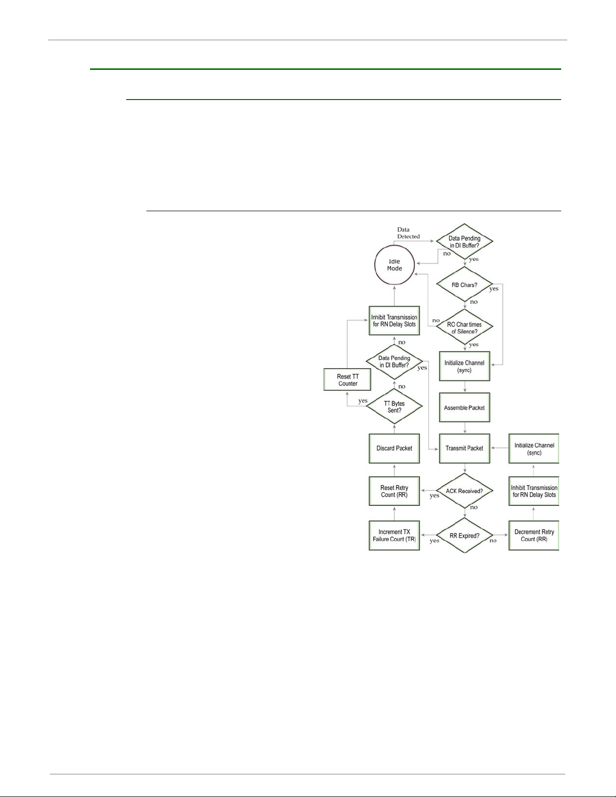
9XTend™ OEM RF Module - Product Manual v2.x6x
Acknowledged Communications
Acknowledged Mode
Attributes:Reliable delivery through positive acknowledgements for each packet
Throughput, latency and jitter vary depending on the quality of the channel and
the strength of the signal.
Required Parameter Values (TX module): RR (Retries) >= 1
Related Commands: Networking (DT, MK, RR), Serial Interfacing (PK, RN, RO, RB, TT)
Recommended Use: Use for applications that require Reliable Delivery. If messages are smaller
than 256 bytes, use RB and RO commands to align RF packets to application packets.
Connection Sequence
Figure 4-07. Acknowledged Mode State
After sending a packet while in
Acknowledged Mode, the TX (transmitting) module listens for an ACK
(acknowledgement). If it receives
the ACK, it will either move on to
sending a subsequent packet (if
more transmit data is pending) or
will wait for exactly RN random delay
slots before allowing another transmission (if no more data is pending
to be transmitted).
If the TX module does not receive
the ACK within the allotted time, it
will retransmit the packet with a new
RF initializer followi
There is no delay between the first
ACK slot and the first retransmission.
Subsequent retransmissions incur a
delay of a random number of delay
slots, between 0 and RN. If RN is set
to 0 on the TX module, there are
never any back-off delays between
retransmissions. Note that during
back-off delays, the TX module will
go into Idle Mode and may receive
RF data. This can have the effect of
increasing the back-off delay, as the
module cannot return to Transmit (or
retransmit) Mode as long as it is receiving RF data.
ter receiving and acknowledging a packet, the RX (receiving) module will move to the next fre-
Af
quency and listen for either a retransmission or new data for a specific period of time. Even if the
TX module has indicated that it has no more pending transmit data, it may not have received the
previous ACK, and so may retransmit the packet, possibly with no delay after the ACK slot. In this
case, the RX module will always detect the immediate retransmission, which will hold off the communications channel and thereby reduce collisions. RX module
they receive, but they only pass the first copy of a packet they receive out the UART.
RB and RO parameters are not applied to subsequent packets, meaning that once transmission
has begun, it will continue uninterrupted until the DI buffer is empty or the streaming limit (TT
parameter) has been reached. As with the first packet, the payload of each subsequent packet
includes up to the maximum packet size (PK parameter), and the TX module checks for more
pending data near the end of each packet.
Diagram (TX module)
ng the ACK slot.
s acknowledge each retransmission
© 2010 Digi Internatonal, Inc. 52
Page 53

9XTend™ OEM RF Module - Product Manual v2.x6x
The TT parameter (streaming limit) specifies the maximum number of bytes that the TX module
will send in one transmission event, which may consist of many packets and retries. If the TT
parameter is reached, the TX module will force a random delay of 1 to RN delay slots (exactly 1
delay slot if RN is zero). Each packet is counted only once toward TT, no matter how many times
the packet is retransmitted.
Subsequent packets in Acknowledged Mode are similar to those in Streaming Mode, with the addition of an ACK between each packet, and the possibilit
are sent without an RF initializer, as the RX modules are already synchronized to the TX module
from the preceding packet(s) and they remain synchronized for the duration of the transmission
event. Each retransmission of a packet includes an RF initializer.
Once the TX module has sent all pending data or has reached the TT limit, the acknowledged
transmission event is completed. The TX module will not transmit again for exactly RN delay slots,
if the local RN parameter is set t
number of delay slots between 0 and (RN-1), if the local RN parameter is set to a non-zero value.
These delays are intended to lessen congestion following long bursts of packets from a single TX
module, during which several RX modules may have themselves become ready to transmit.
y of retransmissions. Subsequent packets
o a non-zero value. The RX module will not transmit for a random
© 2010 Digi Internatonal, Inc. 53
Page 54

9XTend™ OEM RF Module - Product Manual v2.x6x
Polling Mode (Acknowledged)
NOTE: Polling Mode (Acknowledged) and Polling Mode (Basic) [p50] operate in the same way. The
difference between the two modes is in their means of achieving reliable delivery of data. In Polling Mode (Acknowledged), reliable delivery is achieved using retries and acknowledgements.
Attributes:Utilizes high percentage of available network bandwidth
Eliminates collisions
Works with reliable delivery (RR or MT parameters)
Supports binary data transfers
Base module requests packets from remote module by polling a sequential
range of addresses
Base module is con
Uses inter-character delay to create RF packet lengths aligned with protocol
packet lengths up to 2048 bytes long.
Required Parameter Values (Base): MD (RF Mode) = 3, PB (Polling Begin Address), PE (Polling
End Address)
Required Parameter Values (Remote): MD (RF Mode) = 4
Related Commands: Networking (RR, PD, DT, MY, AM)
Constraints: The minimum time interval between polling cycles is configurable. However, if the
remote modules cannot all be processed within tha
(i.e. it will impose no additional delay). In order to ensure a pause between polling cycles, PD
must be set to a value which is large enough to accommodate the pause.
Recommended Use: Use for point-to-multipoint applications that require Reliable Delivery of
data. Use this mode when it is critical that a base module be able to discern data coming from
multiple modules.
figured to specify the range of addresses being polled
t time interval, the polling cycle is ineffective
Theory of Operation
A ‘Polling Base’ module will cycle through a sequential range of addresses. The ‘Polling Base’ will
poll each ‘Polling Remote’ module, wait for a response, then poll the next remote address in the
sequence. Each ‘Polling Remote’ will respond by sending the data from its DI (Data In) buffer following the RB (Packetization Threshold) & RO (Packetization Timeout) parameters. When there is
no eligible data to send, the ‘Polling Remote’ will not respond. The ‘Polling Base’ will poll the next
address in the polling sequence after a short delay.
Polling Base
Set the MD (RF Mode) parameter (MD = 3).
Set MY (Source Address) parameter (MY = 0).
Set the sequential range of Polling Addresses using the PB (Polling Begin Address) and PE
(Polling End Address) parameters.
(Optional) Enable Acknowledged Reliable Delivery (RR >= 0). Note: Basic Reliable Delivery is
also supported. Refer to the ‘Polling Mode - Basic section for more information.
(Optional) Use the PD (Minimum Polling Delay) command to configure a delay between polls to
slow down system (if needed).
(Optiona
basis.
Polling Remote Configuration:
Set the MD (RF Mode) parameter (MD = 4).
Configure sequential source addresses for all remote modules using the MY (Source Address)
command.
Set the DT (Destination Address) parameter to point to ‘Polling Base’ (DT = 0x0000).
(Optional) Enable Acknowledged Reliable Delivery (RR >= 0). Note: Basic Reliable Delivery is
also supported. Refer to the ‘Polling Mode - Basic section for more information.
Configuration:
l) Enable API Mode to address remotes within polling range on a packet-by-packet
© 2010 Digi Internatonal, Inc. 54
Page 55
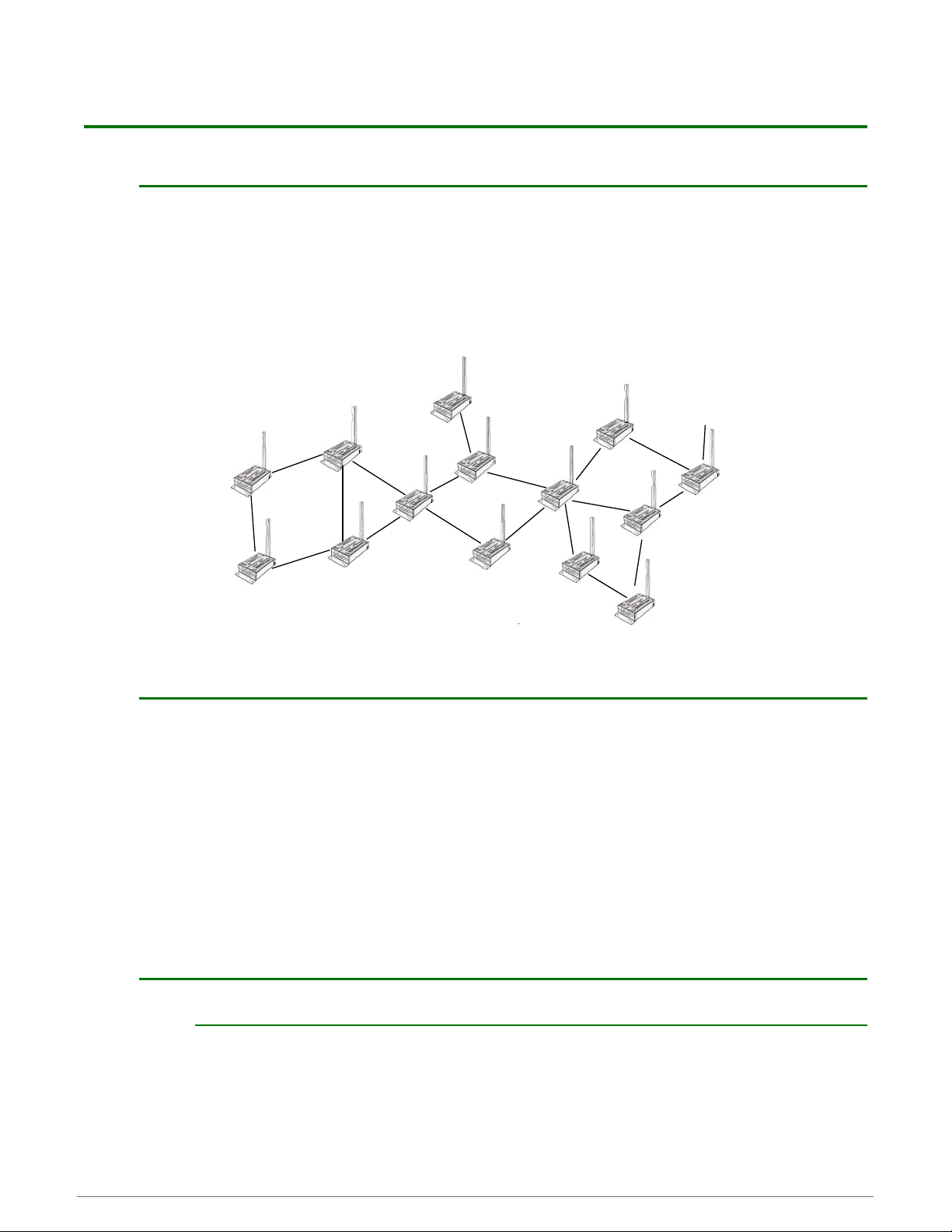
5. DigiMesh™
Introduction
XTend OEM RF Modules containing firmware version 8020 (or above) now feature DigiMesh™
mesh networking support. Mesh networking allows messages to be routed through several different nodes to a final destination. The DigiMesh firmware allows OEMs and system integrators to
bolster their networks with the self-healing attributes of mesh networking. In the event that one
RF connection between nodes is lost (due to power-loss, environmental obstructions, etc.) critical
data can still reach its de
modules.
A Sample DigiMesh Network Topology
stination due to the mesh networking capabilities embedded inside the
DigiMesh Feature Set
XTend OEM RF Modules containing firmware version 8020 (or above) support the following features:
Self-healing - Any node may enter or leave the network at any time without causing the net-
work as a whole to fail.
Peer-to-peer architecture - No hierarchy and no parent-child relationships are needed.
Quiet Protocol - Routing overhead will be reduced by using a reactive protocol similar to
AODV. Rather than maintaining a network map, routes will be discovered and created only
when needed.
Selective acknowledgements - Only the
Unicast and Broadcast addressing supported
Reliable delivery - Reliable delivery of data is accomplished by means of acknowledgements.
Note that Sleep (low power) modes and encryption are not supported in this release.
Data Transmission and Routing
Unicast Addressing
When transmitting while using Unicast communications, reliable delivery of data is accomplished
using retries and acknowledgements. The number of retries is determined by the NR (Network
Retries) parameter. RF data packets are sent up to NR + 1 times and ACKs (acknowledgements)
are transmitted by the receiving node upon receipt. If a network ACK is not received within the
time it would take for a packet to traverse the network twice, a retransmission occurs.
destination node will reply to route requests
© 2010 Digi International Inc. 55
Page 56

9XTend™ OEM RF Module - Product Manual v2.x6x
To send Unicast messages, set the DH and DL on the transmitting module to match the corresponding SH and SL parameter values on the receiving module.
Broadcast Addressing
Broadcast transmissions will be received and repeated by all nodes in the network. Because ACKs
are not used the originating node will send the broadcast four times. Essentially the extra transmissions become automatic retries without acknowledgments. This will result in all nodes repeating the transmission four times as well. In order to avoid RF packet collisions, a random delay is
inserted before each node relays the broadcast message. (See NN parameter for details on chang-
this random delay time.) Sending frequent broadcast transmissions can quickly reduce the
ing
available network bandwidth and as such should be used sparingly.
The broadcast address is a 64 bit address with the lowest 16 bits set to 1. The upper bits are set to
0. To send a broadcast transmission set DH to 0 and DL to 0xFFFF. In API mode the destination
address would be set to 0x000000000000FFFF
Routing
A module within a mesh network is able to determine reliable routes using a routing algorithm and
table. The routing algorithm uses a reactive method derived from AODV (Ad-hoc On-demand Distance Vector). An associative routing table is used to map a destination node address with its next
hop. By sending a message to the next hop address, either the message will reach its destination
or be forwarded to an intermediate node which will route the message on to its destination. A
message with a Broadcast address is bro
rebroadcast the message and eventually the message will reach all corners of the network. Packet
tracking prevents a node from resending a broadcast message twice.
adcast to all neighbors. All receiving neighbors will
Route Discovery
If the source node doesn’t have a route to the requested destination, the packet is queued to
await a route discovery (RD) process. This process is also used when a route fails. A route fails
when the source node uses up its network retries without ever receiving an ACK. This results in
the source node initiating RD.
RD begins by the source node broadcasting a route request (RREQ). Any node that receives the
RREQ that is not the ultimate destination is called an intermediate node.
Intermediate nodes may either drop or forward a RRE
a better route back to the source node. If so, information from the RREQ is saved and the RREQ is
updated and broadcast. When the ultimate destination receives the RREQ, it unicasts a route reply
(RREP) back to the source node along the path of the RREQ. This is done regardless of route quality and regardless of how many times an RREQ has been seen before.
This allows the source node to receive multiple route replies. The source node selects the route
with the best round trip route quality, which i
packets with the same destination address.
RF Module Configuration
Two command mode protocols are supported by this DigiMesh version of the 9XTend RF Module:
AT Command Mode - Printable protocol that is intended for manual entry of commands and
viewing parameter values.
API Operation - Binary protocol intended for programmatic transmissions and receptions of
data packets. For example, using API mode, sequential packets can be sent to different
addresses without having to escape into command mode and change DL between each transmission.
Q, depending on whether the new RREQ has
t will use for the queued packet and for subsequent
AT Commands
To Send AT Commands (Using the 'Terminal' tab of the X-CTU Software):
© 2010 Digi Internatonal, Inc. 56
Page 57

9XTend™ OEM RF Module - Product Manual v2.x6x
Example: Utilize the 'Terminal' tab of the X-CTU Software to change the module's DL (Destination
Address Low) parameter and save the new address to non-volatile memory. This example requires
the installation of MaxStream’s X-CTU Software and a serial connection to a PC.
Select the ‘Terminal’ tab of the X-CTU Software and enter the following command lines:
Method 1 (One line per command)
A
Address Low)
Note: When using X-CTU Software to program a module, PC com port settings must match the
baud (interface data rate), parity & stop bits parameter settings of the module. Use the 'Com Port
Setup' section of the "PC Settings" tab to configure PC com port settings to match those of the
module.
AT Command Reference Table
esnopseR metsySdnammoC TA dneS
lav tnerruc{>retnE< LDT
)edoM dnammoC TA retnE( >RC< KO+++
ov-non ot etirW( >RC< KO>retnE< RWTA
)edoM dnammoC tixE( >RC< KO>retnE< NCTA
noitanitseD daeR( >RC< }eu
)woL sserddA noitanitseD yfidoM( >RC< KO>retnE< D0A10000LDTA
)yromem elital
Table 5-01. Special)
AT Command AT Command Name Parameter Range
PL
R1
RE
WR
FR
9XTend RF Modules expect numerical values in hexadecimal. Hexadecimal values are designated
by a "0x" prefix. Decimal equivalents are designated by a "d" suffix.
TX Power Level. Set/Read the power level at
which the RF module transmits data
Restore Compiled. Restore module
parameters to compiled defaults.
Restore Defaults. Restore module
parameters to custom defaults.
Write. Write configurable parameters to nonvolatile memory
Force Reset. Force module to take a physical
reset.
0 – 4
0 = 1 mW
1 = 10 mW
2 = 100 mW
3 = 500 mW
4 = 1000 mW (1 Watt)
Command
Category
RF Interfacing 1 4 (1 Watt)
# Bytes
Returned
Factory
Default
----)laicepS(--
----)laicepS(--
----)laicepS(--
----)laicepS(--
Table 5-02. Networking
AT
Command
DH
AT Command Name Parameter Range
Destination Address High. Set/Read the
destination address (high 32 bits) of a module.
0 - 0xFFFFFFFF Networking 4
Command
Category
# Bytes
Returned
© 2010 Digi Internatonal, Inc. 57
Factory
efault
D
v8020:
0x0013A200
v8021:
0x00000000
Page 58

9XTend™ OEM RF Module - Product Manual v2.x6x
DL
Destination Address Low. Set/Read the
destination address (low 32 bits) of a module.
0 - 0xFFFFFFFF Networking 4
v8020:
0x00000000
v8021:
0x0000FFF
F
(broadcast)
HP
ID
NH
NN
NQ
NR
Hopping Channel. Set/Read the channel
hopping sequence. Nodes must have the
same hopping sequence to communicate.
Network Address. Set/Read the user
network address. Nodes must have the same
network address to communicate.
Network Hops. Set/Read the maximum
number of hops expected in a network route.
This value doesn't limit the number of
allowed, but it is used to calculate timeouts
waiting for network acknowledgements.
Network Delay Slots. Set/Read the
maximum random number of network delay
slots before re-broadcasting a network packet.
One network delay slot is approximately
168ms.
Network Route Requests. Set/Read the
maximum number of route discovery retries
allowed to find a path to the destination node.
If NQ = 0, a route request will only be sent
once.
Network Retries. Set/Read the maximum
number of network packet delivery atte
NR > 0, packets sent will request a network
ACK and can be resent up to NR+1 times if no
ACKs are received.
hops
mpts. If
0 - 9 Networking 1 0
0x10 - 0x7FFF Networking 2 0x3332
0 – 0xFF
[Max number of hops]
0 – 0x10 Networking 2 3
0 – 0x0A Networking 2 3
0 – 0xFF Networking 2 1
Networking 2 7
SH
SL
Table 5-03. )Diagnostics
AT
Command
AT
BT
CC
CN
Source Address High. Set/Read the source
address (high 32 bits) of a module.
Source Address Low. Set/Read the source
address (low 32 bits) of a module.
AT Command Name
Guard Time After. Set/Read required DI pin silent time
after the Command Sequence Characters of the
Command Mode Sequence. The DI silent time is used to
prevent inadvertent entrance into Command Mode.
Guard Time Before. Set/Read required DI pin silent time
before the Command Sequence Characters of the
Command Mode Sequence. The DI silent time is used to
prevent inadvertent entrance into Command Mode.
Command Sequence Character. Set/Read the ASCII
character used
Mode Sequence (BT + CC + AT)
Exit Command Mode. Explicitly exit the module from AT
Command Mode. (The same action occurs automatically
when CT expires.)
between guard times of the AT Command
0x0013A200
[read-only]
0 - 0xFFFFFFFF
[read-only]
Parameter
Range
0 – 0xFFFF
[x 100 msec]
0 - 0xFFFF
[x 100 msec]
0x20 - 0x7F
--
Networking 2 0x0013A200
Networking 2 varies
Command
Category
Command Mode
Options
Command Mode
Options
Command Mode
Options
Command Mode
Options
# Bytes
Returned
2
2 0x0A (10d)
1
-- --
Factory
Default
0x0A
(1 decimal
second)
0x2B
[ASCII "+"]
© 2010 Digi Internatonal, Inc. 58
Page 59

9XTend™ OEM RF Module - Product Manual v2.x6x
CT
E0
E1
Table 5-04. Diagnostics
AT
Command
CF
DB
Command Mode Timeout. Set/Read the amount of
inactive time that elapses before the module automatically
exits from AT Command Mode.
Echo Off. Turn off character echo in AT Command Mode.
By default, echo is off.
Echo On. Turn on character echo in AT Command Mode.
Each input character is echoed back to out to the host.
AT Command Name Parameter Range
0 – 2
Command Format. Set/Read the format of
data entered and displayed for commands.
Use decimal format unless Hex is forced or
preferred.
Received Signal Strength. Read the receive
signal strength (in decibels relative to
milliWatts) of the last received packet.
0 = Decimal with units
1 - Hexadecimal
without units. All input
and output is in
hexadecimal format.
2 - Decimal without
units.
0x6E - 0x28 [read-only]
Sample Output:
-88 dBm (when ATCF =
0)
58 (when ATCF = 1)
-88 (when
2 - 0xFFFF
[x 100 ms]
--
--
ATCF = 2)
Command Mode
Options
Command Mode
Options
Command Mode
Options
Command
Category
Diagnostics 1 1
Diagnostics 2 --
2 0xC8 (200d)
-- --
-- --
# Bytes
Returned
Factory
Default
--4scitsongaiDAFFB5x0 ot ACC2x0egatloV draoBV%
ER
GD
HV
RC
RM
RP
TP
TR
VL
Receive Error Count. Set/Read the number
of receive-errors.
Receive Good Count. Set/Read the count of
good received RF packets.
Hardware Version Read and display the
version of the hardware
Ambient Power - Single Channel. Examine
& report the power level on a given channel.
Ambient Power - All Channels. Examine and
report power level
RSSI PWM Timer. Enable PWM ("Pulse
Width Modulation") output on the Config/RSSI
pin (pin 11 of the OEM RF Module)
Board Temperature. Read the current
temperature of the board.
Delivery Failure Count. Report the number of
retransmit failures.
Firmware Version – verbose. Read detailed
version information including application build
date and time.
s on all channels.
0 - 0xFFFF Diagnostics 2 0
0 - 0xFFFF Diagnostics 2 0
0 – 0Xffff Diagnostics 2 --
0 - 0x31 [dBm, read-only]
Sample output:
-78 dBm [when CF = 0]
4e [when CF = 1]
-78 [when CF = 2]
No parameter - 0x7D0 Diagnostics 2 --
0 - 0xFF [x 100 msec] Diagnostics 1 0x20 (32d)
0 - 0x7F [read-only] Diagnostics 1 --
0 - 0xFFFF [read-only] Diagnostics 2 0
Returns string Diagnostics -- --
Diagnostics 1 --
© 2010 Digi Internatonal, Inc. 59
Page 60

9XTend™ OEM RF Module - Product Manual v2.x6x
VR
WA
WN
WS
Firmware Version. Read the 4-digit version
number.
Active Warning Numbers. Report the
warning numbers of all active warnings - one
warning number per line.
Warning Data. Report data for all active and
sticky warnings
Sticky Warning Numbers. Report warning
numbers of all warnings active since the last
use of the WS or WN command
0 - 0xFFFF [read-only] Diagnostics 2 --
Returns string Diagnostics -- --
Returns string Diagnostics -- --
Returns string Diagnostics -- --
© 2010 Digi Internatonal, Inc. 60
Page 61

9XTend™ OEM RF Module - Product Manual v2.x6x
Table 5-05. Serial Interfacing
AT
Command
AP
BD
CD
AT Command Name Parameter Range
0 – 2
API Enable. Set/Read the API mode of the
radio.
Interface Data Rate. Set/Read the serial
interface data rate (baud rate) used between
the RF module and host.
GPO2 Configuration. Select/Read the
behavior of the GPO2 line (pin 3).
0 = API Disabled
1 = API-enabled
2 = API-enabled
(w/escaped control characters)
0 - 8 (standard rates)
0 = 1200 bps
1 = 2400
2 = 4800
3 = 9600
4 = 19200
5 = 38400
6 = 57600
7 = 115200
8 = 230400
0x39 - 0x1C9C38 (non-standard
rates)
0 – 4
0 = RX LED (when data is received
whether or not the address is valid.)
1 = Assert RX LED
2 = De-assert RX LED
3 = (reserved)
4 = RX LED (valid address only)
Command
Category
Serial
Interfacing
Serial
Interfacing
Serial
Interfacing
# Bytes
Return
ed
10
4
12
Factory
Default
3
(9600 baud)
CS
FL
FT
NB Parity. Select/Read parity settings.
RB
GPO1 Configuration. Select/Read the
behavior of the GP01 pin (pin 9)
Software Flow Control. Enable/Disable
software flow control (XON/XOFF).
Flow Control Threshold. Set/Read the flow
control threshold. When FT b
accumulated in the DI buffer (UART Receive),
CTS is de-asserted or the XOFF software flow
control character is transmitted.
Packetization Threshold. Set/Read the
character threshold value. RF transmission
begins after receiving RB bytes, or after
receiving at least 1 byte and detecting RO
character times of silence on the UART.
ytes have
0 – 4
0 = RS-232 CTS flow control
1 = RS-485 TX enable low
2 = CTS always High
3 = RS-485 TX enable high
4 = CTS always Low
0 – 1
0 = Disabled
1 = Enabled
0x10 – 0x17E
[Bytes]
0 – 4
0 = No parity
1 = 8-bit even
2 = 8-bit odd
3 = Forced high
4 = Forced low
0 – 0xD3
[Bytes]
Serial
Interfacing
Serial
Interfacing
Serial
Interfacing
Serial
Interfacing
Serial
Interfacing
10
10
2
10
2
0x16D
(365
decimal)
0xC8
(200
decimal)
© 2010 Digi Internatonal, Inc. 61
Page 62
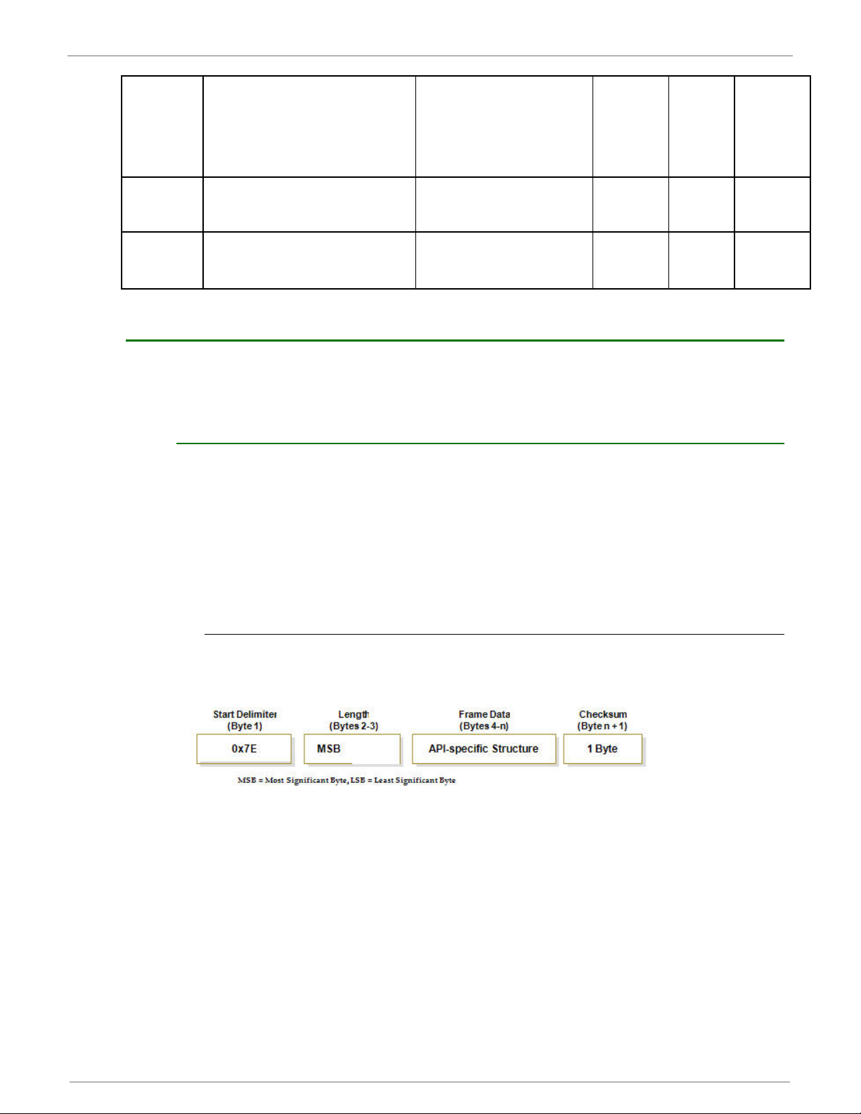
9XTend™ OEM RF Module - Product Manual v2.x6x
Packetization Timeout. Set/Read the
number of character times with no UART data
RO
before a packet is created for RF output
(assuming UART data was received prior to
the idle time). If RO = 0, it is ignored and no
data will be transmitted until RB characters
are in the DO buffer.
0 - 0xFFFF
[x UART character time]
Serial
Interfacing
23
RT
SB
GPI1 Configuration. Set/Read the behavior
f the GPI1 pin (pin 10).
o
Stop Bits. Set/Read the number of stop bits in
the data packet.
API Operation
API operation requires that communication with the module be done through a structured interface (data is communicated in frames in a defined order). The API specifies how commands, command responses and module status messages are sent and received from the module using a
UART data Frame.
API Frame Specifications
Two API modes are supported and both can be enabled using the AP (API Enable) command. Use
the following AP parameter values to configure the module to operate in a particular mode:
"AP = 0 (default): Transparent Operation (UART Serial line replacement)
API modes are disabled.
AP = 1: API Operation
AP = 2: API Operation (with escaped characters)
Any data received prior to the start delimiter is silently discarded. If the frame is not received correctly or if the checksum fails, the data is silent
0 – 2
0 = No RTS flow control 2 = RTS
flow control
0 – 1
0 = 1 stop bit
1 = 2 stop bits
ly discarded.
Serial
Interfacing
Serial
Interfacing
10
10
API Operation (AP parameter = 1)
When this API mode is enabled (AP = 1), the UART data frame structure is defined as follows:
Figure 5-01. UART Data Frame Structure
© 2010 Digi Internatonal, Inc. 62
Page 63
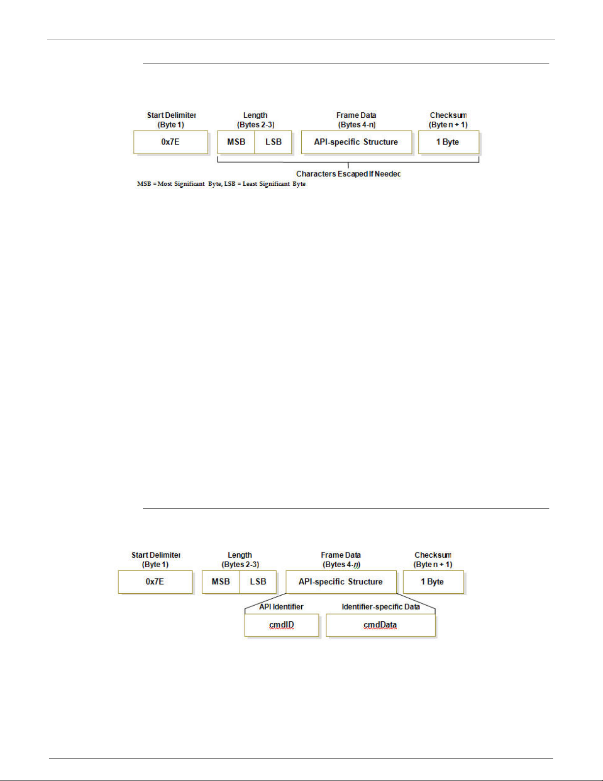
9XTend™ OEM RF Module - Product Manual v2.x6x
API Operation - with Escape Characters (AP parameter = 2)
When this API mode is enabled (AP = 2), the UART data frame structure is defined as follows:
Figure 5-02. UART Data Frame Structure - with escape control characters
Escape characters. When sending or receiving a UART data frame, specific data values must be
escaped (flagged) so they do not interfere with the UART or UART data frame operation. To escape
an interfering data byte, insert 0x7D and follow it with the byte to be escaped XOR'd with 0x20.
Data bytes that need to be escaped:
0x7E - Frame Delimiter
0x7D - Escape
0x11 - XON
0x13 - XOFF
Example - Raw UART Data Frame (before escaping interfering bytes):
0x7E 0x00 0x02 0x23 0x11 0xCB
0x11 needs to be escaped which results in the following frame:
0x7E 0x00 0x02 0x23 0x7D 0x31 0xCB
Note: In the above example, the length of the raw data (excluding the checksum) is 0x0002 and
the checksum of the non-escaped data (excluding frame delimiter and length) is calculated as:
0xFF - (0x23 + 0x11) = (0xFF - 0x34) = 0xCB.
Checksum
To test data integrity, a checksum is calculated and verified on non-escaped data.
alculate: Not including frame delimiters and length, add all bytes keeping only the lowest 8
To c
bits of the result and subtract from 0xFF.
To verify: Add all bytes (include checksum, but not the delimiter and length). If the checksum is
correct, the sum will equal 0xFF.
API Types
Frame data of the UART data frame forms an API-specific structure as follows:
Figure 5-03. UART Data Frame & API-specic Structure
The cmdID frame (API-identifier) indicates which API messages will be contained in the cmdData
frame (Identifier-specific data). Refer to the sections that follow for more information regarding
the supported API types. Note that multi-byte values are sent big endian.
© 2010 Digi Internatonal, Inc. 63
Page 64
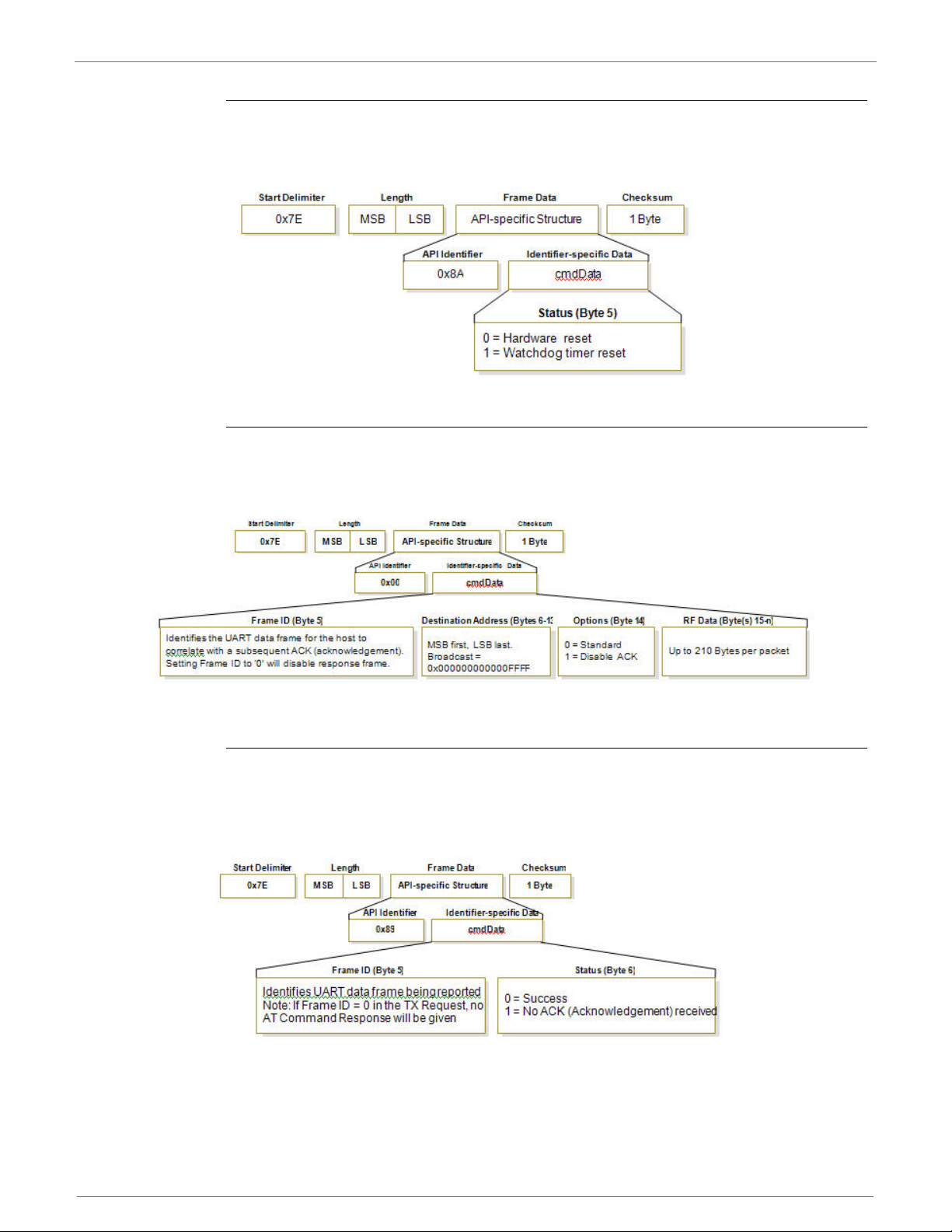
9XTend™ OEM RF Module - Product Manual v2.x6x
RF Module Status
API Identifier: 0x8A
RF module status messages are sent from the module in response to specific conditions.
Figure 5-04. RF Module Status Frames
TX (Transmit) Request: 64-bit address
API Identifier Value: 0x00
A TX Request message will cause the module to send RF Data as an RF Packet
Figure 5-05. TX Packet (64-bit address) Frames
TX (Transmit) Status
API Identifier Value: 0x89
When a TX Request is completed, the module sends a TX Status message. This message will indicate if the packet was transmitted successfully or if there was a failure.
Figure 5-06. TX Status Frames
NOTE: "STATUS = 1" occurs when all retries are expired and no ACK is received.
© 2010 Digi Internatonal, Inc. 64
Page 65

9XTend™ OEM RF Module - Product Manual v2.x6x
RX (Receive) Packet: 64-bit address
API Identifier Value: 0x80
When the module receives an RF packet, it is sent out the UART using this message type.
Figure 5-07. RX Packet (16-bit address) Frames
© 2010 Digi Internatonal, Inc. 65
Page 66

Appendix A: Agency
FCC (United States) Certification
The XTend OEM RF Module complies with Part 15 of the FCC rules and regulations. Compliance
with the labeling requirements, FCC notices and antenna usage guidelines is required.
In order to operate under Digi’s FCC Certification, OEMs/integrators must comply with the following regulations:
1. The OEM/integrator must ensure that the text provided with t
placed on the outside of the final product and within the final product operation manual.
2. The XTend OEM RF Module may only be used with antennas that have been tested and
approved for use with this module [
refer to ‘FCC-approved Antennas’ section].
OEM Labeling Requirements
WARNING: The Original Equipment Manufacturer (OEM) must ensure that FCC labeling
requirements are met. This includes a clearly visible label on the outside of the final
product enclosure that displays the text shown in the figure below.
Figure A-01. Required FCC el OEM duct ntining the XTend OEM RF dule
Contains FCC ID: OUR-9XTEND
The enclosed device complies with Part 15 of the FCC Rules. Operation is subject to the following two
conditions: (i.) this device may not cause harmful interference and (ii.) this device must accept any interference received, including interference that may cause undesired
operation.
his device [Figure A-01] is
FCC Notices
IMPORTANT: The XTend OEM RF Module has been certified by the FCC for use with other prod-
ucts without any further certification (as per FCC section 2.1091). Modifications not expressly
approved by Digi could void the user's authority to operate the equipment.
IMPORTANT: OEMs must test final product to comply with unintentional radiators (FCC section
15.107 & 15.109) before declaring compliance of their final product to Part 15 of the FCC
IMPORTANT: The RF module has been certified for remote and base radio applications. If the
module will be used for portable application
This equipment has been tested and found to comply with the limits for a Class B digital device,
pursuant to Part 15 of the FCC Rules. These limits are designed to provide reasonable protection
against harmful interference in a residential installation. This equipment generates, uses and can
radiate radio frequency energy and, if not installed
may cause harmful interference to radio communications. However, there is no guarantee that
interference will not occur in a particular installation
If this equipment does cause harmful interference to radio or television reception, which can be
determined by turning the equipment off and on, the user is encouraged to try to correct the interference by one or more of the following measures: Re-orient or relocate the receiving antenna,
Increas
outlets on different circuits, or Consult the dealer or an experienced radio/TV technician for help.
e the separation between the equipment and receiver, Connect equipment and receiver to
s, the device must undergo SAR testing.
and used in accordance with the instructions,
.
Rules.
© 2010 MaxStream, Inc. 66
Page 67

9XTend™ OEM RF Module - Product Manual v2.x6x
Limited Modular Approval
Power output is conducted at the antenna terminal and can be adjusted from 1 mill-watt to 1 Watt
at the OEM level. This is an RF module approved for Limited Modular use operating as a mobile
transmitting device with respect to section 2.1091 and is limited to OEM installation for Mobile and
Fixed applications only. During final installation, end-users are prohibited from access to any programming parameters. Professional installation adjustment is required for setting module power
and ant
Final antenna installation and operating configurations of this transmitter including antenna gain
and cable loss must not exceed the EIRP of the configuration used for calculating MPE. Grantee
(Digi) must coordinate with OEM integrators to ensure the end-users and installers of products
operating with the module are provided
ments.
The FCC grant is valid only when the device is sold to OEM
to ensure the end-user has no manual instructions to remove, adjust or install the device.
enna gain to meet EIRP compliance for high gain antenna(s).
FCC-approved Antennas
WARNING: This device has been tested with Reverse Polarity SMA connectors with the
antennas listed in the tables of this section. When integrated into OEM products, fixed
antennas require installation preventing end-users from replacing them with nonapproved antennas. Antennas not listed in the tables must be tested to comply with FCC
Section 15.203 (unique antenna connectors) and Section 15.247 (emissions).
with operating instructions to satisfy RF exposure require-
integrators. Integrators are instructed
Fixed Base Station and Mobile Applications
Digi RF Modules are pre-FCC approved for use in fixed base station and mobile applications. When
the antenna is mounted at least 20cm (8") from nearby persons, the application is considered a
mobile application.
Portable Applications and SAR Testing
When the antenna is mounted closer than 20cm to nearby persons, then the application is considered "portable" and requires an additional test be performed on the final product. This test is
called Specific Absorption Rate (SAR) testing and measures the emissions from the module and
how they affect the person.
RF Exposure
This statement must be included as a CAUTION statement in OEM product manuals.
WARNING: This equipment is approved only for mobile and base station transmitting
devices. Antenna(s) used for this transmitter must be installed to provide a separation
distance of at least 30 cm from all persons and must not be co-located or operating in
conjunction with any other antenna or transmitter.
NOTE: The separation distance indicated in the above is 30 cm, but any distance greater than or
equal to 23 cm can be used (per MPE evaluation).
© 2010 MaxStream, Inc. 67
Page 68

9XTend™ OEM RF Module - Product Manual v2.x6x
Antenna Options (1-watt transmit power output or lower)
The antennas in the tables below have been approved for use with this module. Digi does not carry all of these antenna variants. Contact Digi Sales for available antennas.
Half-wave antennas (approved when operating at 1-
Part Number Type Connector Gain Application
A09-HSM-7 Straight half-wave RPSMA 3.0 dBi Fixed / Mobile
A09-HASM-675 Articulated half-wave RPSMA 2.1 dBi Fixed / Mobile
A09-HABMM-P6I Articulated half-wave w/ 6" pigtail MMCX 2.1 dBi Fixed / Mobile
A09-HABMM-6-P6I Articulated half-wave w/ 6" pigtail MMCX 2.1 dBi Fixed / Mobile
A09-HBMM-P6I Straight half-wave w/ 6" pigtail MMCX 2.1 dBi Fixed / Mobile
A09-HRSM Right angle half-wave RPSMA 2.1 dBi Fixed
A09-HASM-7 Articulated half-wave RPSMA 2.1 dBi Fixed
A09-HG Glass mounted half-wave RPSMA 2.1 dBi Fixed
A09-HATM Articulated half-wave RPTNC 2.1 dBi Fixed
A09-H Half-wave dipole RPSMA 2.1 dBi Fixed
Yagi antennas (approved
Part Number Typ e Connector Gain Required Antenna Cable Loss Application
A09-Y6 2 Element Yagi RPN 6.1 dBi 0.1 dB* Fixed / Mobile
A09-Y7 3 Element Yagi RPN 7.1 dBi 1.1 dB* Fixed / Mobile
A09-Y8 4 Element Yagi RPN 8.1 dBi 2.1 dB* Fixed / Mobile
A09-Y6TM 2 Element Yagi RPTNC 6.1 dBi 0.1 dB* Fixed / Mobile
A09-Y7TM 3 Element Yagi RPTNC 7.1 dBi 1.1 dB* Fixed / Mobile
A09-Y8TM 4 Element Yagi RPTNC 8.1 dBi 2.1 dB* Fixed / Mobile
A09-Y15TM
Omni-directional base station antennas (approved when operating at 1-
Part Number Ty pe Connector Gain Required Antenna Cable Loss Application
0A
when operating at 1-
15 Element Yagi RPTNC 15.1 dBi 9.1 dB* Fixed / Mobile
esaB ssalgrebiF4F-90A
ssalgrebiF6F-90A
B ssalgrebiF8F-90A
tS esa
F0F-90A
power output or lower)
power output or lower)
power output or lower)
2NPRnoitatS esaB ssalgrebiF2F-90A
Bd 1.5AMSPRnoitatS esaB ssalgrebiF5F-90A
1.1iBd 1.7AMSPRnoitatS esaB ssalgrebiF7F-90A
d 0.1CNTPRnoitatS esaB ssalgrebiFMT1F-90A
.3CNTPRnoitatS esaB ssalgrebiFMT3F-90A
NTPRnoitatS esaB ssalgrebiFMT5F-90A
1iBd 1.7CNTPRnoitatS esaB ssalgrebiFMT7F-90A
dexiF-iBd 0NPRnoitatS esaB ssalgrebiF0F-90A
dexiF-iBd 0.1NPRnoitatS esaB ssalgrebiF1F-90A
dexiF-iBd 1.
dexiF-iBd 1.3NPRnoitatS esaB ssalgrebiF3F-90A
dexiF-iBd 1.4NPRnoitatS
dexiF-iBd 1.5NPRnoitatS esaB ssalgrebiF5F-90A
dexiF*Bd 1.0iBd 1.6NPRnoitatS esaB
dexiF*Bd 1.1iBd 1.7NPRnoitatS esaB ssalgrebiF7F-90A
dexiF*Bd 1.2iBd 1.8NPRnoita
dexiF*Bd 1.1iBd 1.7NPRnoitatS esaB eriW7W-90A
dexiF-iBd 0AMSPRnoitatS esaB ssalgrebi
dexiF-iBd 0.1AMSPRnoitatS esaB ssalgrebiF1F-90A
dexiF-iBd 1.2AMSPRnoitatS esaB ssalgrebiF2F-90A
dexiF-iBd 1.3AMSPRnoitatS esaB ssalgrebiF3F-90A
dexiF-iBd 1.4AMSPRnoitatS esaB ssalgrebiF4F-90A
dexiF-i
dexiF*Bd 1.0iBd 1.6AMSPRnoitatS esaB ssalgrebiF6F-9
dexiF*Bd
dexiF*Bd 1.2iBd 1.8AMSPRnoitatS esaB ssalgrebiF8F-90A
iF*Bd 1.1iBd 1.7AMSPRnoitatS esaB eriWMS7W-90A
dex
dexiF-iBd 0CNTPRnoitatS esaB ssalgrebiFMT0F-90A
dexiF-iB
dexiF-iBd 1.2CNTPRnoitatS esaB ssalgrebiFMT2F-90A
dexiF-iBd 1
dexiF-iBd 1.4CNTPRnoitatS esaB ssalgrebiFMT4F-90A
dexiF-iBd 1.5C
dexiF*Bd 1.0iBd 1.6CNTPRnoitatS esaB ssalgrebiFMT6F-90A
dexiF*Bd 1.
dexiF*Bd 1.2iBd 1.8CNTPRnoitatS esaB ssalgrebiFMT8F-90A
xiF*Bd 1.1iBd 1.7CNTPRnoitatS esaB eriWMT7W-90A
de
* FCC regulations stipulate a 36 dBm EIRP power requirement. Users implementing antenna gain greater than 6.0 dB must compensate for the
added gain with cable loss. When operating at 1 W power output, the sum (i
n dB) of cable loss and antenna gain shall not exceed 6.0 dB.
© 2010 MaxStream, Inc. 68
Page 69

9XTend™ OEM RF Module - Product Manual v2.x6x
Mag Mount antennas (approved when operating at 1-wa power output or lower)
Part Number Ty pe Connector Gain Required Antenna Cable Loss Application
90A
MSPRtnuoM gaMMS8M-90A
3CNTPRtnuoM gaMMT3M-90A
M-90A
dexiF-iBd 0AMSPRtnuoM gaMMS0M-90A
dexiF-iBd 1.2AMSPRtnuoM gaMMS2M-90A
dexiF-iBd 1.3AMSPRtnuoM gaMMS3MdexiF-iBd 1.5AMSPRtnuoM gaMMS5M-90A
dexiF*Bd 1.1-iBd 1.7AMSPRtnuoM gaMMS7M-90A
dexiF*Bd 1.2-iBd 1.8A
dexiF-iBd 0CNTPRtnuoM gaMMT0M-90A
dexiF-iBd 1.2CNTPRtnuoM gaMMT2M-90A
dexiF-iBd 1.
dexiF-iBd 1.5CNTPRtnuoM gaMMT5M-90A
dexiF*Bd 1.1-iBd 1.7CNTPRtnuoM gaMMT7
exiF*Bd 1.2-iBd 1.8CNTPRtnuoM gaMMT8M-90A
d
Multi-path antennas (approved when operating at 1-
power output or lower)
Part Number Typ e Connector Gain Application
A09-DPSM-P12F omni directional permanent mount w/ 12ft pigtail RPSMA 3.0 dBi Fixed
A09-D3NF-P12F omni directional magnetic mount w/ 12ft pigtail RPN 3.0 dBi Fixed
A09-D3SM-P12F omni directional w/ 12ft pigtail RPSMA 3.0 dBi Fixed
A09-D3PNF omni directional permanent mount RPN 3.0 dBi Fixed
A09-D3TM-P12F omni directional w/ 12ft pigtail RPTNC 3.0 dBi Fixed
A09-D3PTM omni directional permanent mount RPTNC 3.0 dBi Fixed
A92-D4PNF 900 MHz / 2.4GHz permanent mount RPN 2.1 dBi Fixed
A92-D4P 900 MHz / 2.4GHz permanent mount RPSMA 2.1 dBi Fixed
A92-D4PTM 900 MHz / 2.4GHz permanent mount RPTNC 2.1 dBi Fixed
* FCC regulations stipulate a 36 dBm EIRP power requirement. Users implementing antenna gain greater than 6.0 dB must compensate for the
added gain with cable loss. When operating at 1 W power output, the sum (in dB) of cable loss and antenna gain shall not exceed 6.0 dB.
Antenna Options (100 mW transmit power output or lower)
Half-wave antennas (approved when operating at 100 mW
power output or lower)
Part Number Typ e Connector Gain Application
eliboM / dexiFiBd 9.1tnenamrePeriw evaw-retrauQWQ-90A
A09-QRAMM 3 " Quarter-wave wire MMCX 2.1 dBi Fixed / Mobile
A09-QSM-3 Quarter-wave straight RPSMA 1.9 dBi Fixed / Mobile
A09-QSM-3H Heavy duty quarter-wave straight RPSMA 1.9 dBi Fixed / Mobile
A09-QBMM-P6I Quarter-wave w/ 6" pigtail MMCX 1.9 dBi Fixed / Mobile
A09-QHRN Miniature Helical Right Angle solder Permanent -1 dBi Fixed / Mobile
A09-QHSN Miniature Helical Right Angle solder Permanent -1 dBi Fixed / Mob
MSHQ-90A
giR "22-MSRHQ-90A
071-MSRHQ-90A
ile
eliboM / dexiFiBd 9.1AMSPRthgiartS "22-
eliboM / dexiFiBd 9.1AMSPRelgna th
eliboM / dexiFiBd 9.1AMSPRelgna thgiR "7.1
A09-QRSM-380 3.8" Right angl eliboM / dexiFiBd 9.1AMSPRe
A09-QAPM-520 5.2" Articulated Screw mount Permanent 1.9 dBi Fixed / Mobile
A09-QSPM-3 3" Straight screw mount Permanent 1.9 dBi Fixed / Mobile
A09-QAPM-3 3" Articulated screw mount Permanent 1.9 dBi Fixed / Mobile
A09-QAPM-3H 3" Articulate
d screw mount Permanent 1.9 dBi Fixed / Mobile
© 2010 MaxStream, Inc. 69
Page 70

9XTend™ OEM RF Module - Product Manual v2.x6x
Yagi antennas (approved when operating at 100 mW power output or lower)
Part Number Typ e Connector Gain Application
iFiBd 1.8NPRigaY tnemelE 48Y-90A
igaY tnemelE 501Y-90A
elE 721Y-90A
-90A
IC (Industry Canada) Certification
0141Y
iBd 1.9CNTPRigaY tnemelE 4MT9Y-90A
1.11CNTPRigaY tnemelE 6MT11Y-90A
1.31CNTPRigaY tnemelE 9MT31Y-90A
1.41CNTPRigaY tnemelE 21MT41Y-90A
1.51CNTPRigaY tnemelE 51MT51Y-90A
eliboM / dexiFiBd 1.6NPRigaY tnemelE 26Y-90A
eliboM / dexiFiBd 1.7NPRigaY tnemelE 37Y-90A
eliboM / dex
eliboM / dexiFiBd 1.9NPRigaY tnemelE 49Y-90A
eliboM / dexiFiBd 1.01NPR
eliboM / dexiFiBd 1.11NPRigaY tnemelE 611Y-90A
eliboM / dexiFiBd 1.21NPRigaY tnem
eliboM / dexiFiBd 1.31NPRigaY tnemelE 931Y-90A
eliboM / dexiFiBd 1.41NPRigaY tnemelE
eliboM / dexiFiBd 1.41NPRigaY tnemelE 2141Y-90A
eliboM / dexiFiBd 1.51NPRigaY tnemelE 3151Y-90A
eli
boM / dexiFiBd 1.51NPRigaY tnemelE 5151Y-90A
eliboM / dexiFiBd 1.6CNTPRigaY tnemelE 2MT6Y-90A
dexiFiBd 1.7CNTPRigaY tnemelE 3MT7Y-90A
eliboM /
eliboM / dexiFiBd 1.8CNTPRigaY tnemelE 4MT8Y-90A
eliboM / dexiF
eliboM / dexiFiBd 1.01CNTPRigaY tnemelE 5MT01Y-90A
/ dexiFiBd
eliboM
eliboM / dexiFiBd 1.21CNTPRigaY tnemelE 7MT21Y-90A
eliboM / dexiFiBd
eliboM / dexiFiBd 1.41CNTPRigaY tnemelE 01MT41Y-90A
eliboM / dexiFiBd
eliboM / dexiFiBd 1.51CNTPRigaY tnemelE 31MT51Y-90A
eliboM / dexiFiBd
Labeling Requirements
Labeling requirements for Industry Canada are similar to those of the FCC. A clearly visible label
on the outside of the final product enclosure must display the following text:
Contains Model 9XTend Radio, IC: 4214A-9XTEND
The integrator is responsible for its product to comply with IC ICES-003 & FCC Part 15, Sub. B Unintentional Radiators. ICES-003 is the same as FCC Part 15 Sub. B and Industry Canada accepts
FCC test r
eport or CISPR 22 test report for compliance with ICES-003.
C-TICK (Australia) Certification
Power Requirements
Regulations in Australia stipulate a maximum of 30 dBm EIRP (Effective Isotropic Radiated Power).
The EIRP equals the sum (in dBm) of power output, antenna gain and cable loss and cannot not
exceed 30 dBm.
Figure A-02. EIRP Formula for Australia
NOTE: The maximum EIRP for the FCC (United States) and IC (Canada) is 36 dBm.
Models with ware comply with requirements to be used in end products in Australia. All products with EMC
and radio communications must have a registered C-Tick mark. Registration to use the compliance mark will only be accepted
from Australian manufacturers or importers, or their agent, in Australia. In order to have a C-Tick mark on an end product, a
company must comply with (a) or (b) below.
(a) have a company presence in Australia
(b) have a company/distributor/agent in Australia that will sponsor the importing of said product
Contact Digi for questions related to locating a contact in Australia.
© 2010 MaxStream, Inc. 70
Page 71

Appendix B: Development Guide
Development Kit Contents
The 9XTend Development Kit includes the hardware and software needed to rapidly create long
range wireless links between devices.
Table B-01. XTend Development Kit Contents
Item Qty. Description Part Number
XTend OEM RF Module 1 Long Range 900 MHz RF Module (w/ RPSMA Connector) XT09-SI
XTend OEM RF Module 1 Long Range 900 MHz RF Module (w/ MMCX antenna) XT09-MI
Antenna 1 900 MHz RPSMA, 6" Half-Wave, dipole, articulating, RPSMA A09-HASM-675
Antenna 1 900 MHz RPSMA, 7" Half-Wave, dipole, articulating, w/ pigtail, MMCX A09-HABMM-P5I
RS-232 Interface Board 2 Enables comm R-BITXsecived 232-SR ot noitacinu
RS-232 Cable (6') 2 Connects interface board to devices having an RS-232 serial port JD2D3-CDS-6F
Serial Loopback Adapter 1
NULL Modem Adapter
(male-to-male)
NULL Modem Adapter
(female-to-female)
Male DB-9 to RJ-45
Adapter
Female DB-9 to RJ-45
Adapter
Power Adapter 2
CD 1 Contains documentation, software and tools needed for RF operation. MD0010
Quick Start Guide 1 Familiarizes users with some of the module's most important functions. MD0016
Connects to the female RS-232 (DB-9) serial connector of the
MaxStream Interface
to function as a repeater (for range testing)
Connects to the female RS-232 (DB-9) serial connector of the
1
MaxStream Interface Board and can be used to connect the module to
another DCE (female DB9) device
1 Used to bypass radios to verify serial cabling is functioning properly JD3D3-CDN-A
Facilitates adapting the DB-9 Connector of the MaxStream Interface
1
Board to a CAT5 cable (male DB9 to female RJ45)
Facilitates adapting the DB-9 Connector of the MaxStream Interface
1
Board to a CAT5 cable (female DB9 to female RJ45)
Allows Interface Board to be powered by a 110 Volt AC power supply
(not included with international (-INT) development kits)
Board and can be used to configure the module
JD2D3-CDL-A
JD2D2-CDN-A
JE1D2-CDA-A
JE1D3-CDA-A
JP4P2-9V10-6F
Interfacing Hardware
The XTend Development Kit includes a pair of RS-232 interface boards that supports the RS-232/
485/422 protocols. When the modules are mounted to the interface boards, the boards provide
the following development tools:
Fast and direct connection to serial devices (such as PCs) and therefore easy access to the
module registries - The parameters stored in the registry allow OEMs and integrators to customize the modules to suite the specific needs of their data systems.
External DIP switch for automatic configuration of commonly used mo
Conversion of signals between TTL levels and RS-232 levels
The MaxStream Interface board provides means for connecting the module to any device that has
an available RS-232 or RS-485/422 connection. The following sections illustrate how to use the
interface boards for development purposes.
Note: In the sections the follow, an OEM RF module mounted to an interface board will be referred to
as a "Module Assembly".
© 2010 Digi International Inc. 71
dule profiles
Page 72
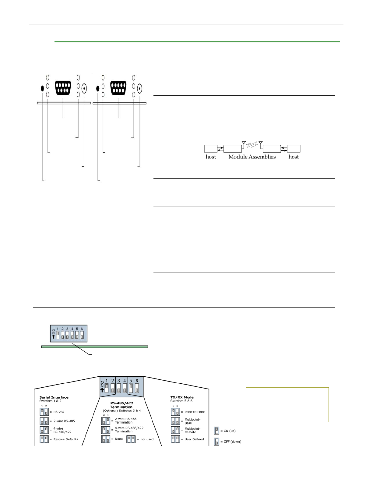
9XTend™ OEM RF Module - Product Manual v2.x6x
XTIB-R RS-232/485 Interface Board
B-01a. Config (Configuration) Switch
Figure B-01. Front View
B-01c.
DB-9 Serial Port
B-01b.
I/O & Power LEDs
B-01a.
Cong Switch
B-01d
RSSI LEDs
B-01e.
Power Connector
The Config Switch provides an alternate method for entering into
Command Mode. To enter Command Mode at the module's default RF
data rate, hold the Configuration Switch down for two seconds.
B-01b. I/O & Power LEDs
The LEDs visualize gigantic status information and indicate module
activity as follows:
Yellow (top LED) = Serial Data Out (to host)
Green (middle) = Serial Data In (from host)
Red (bottom) =
powered; it pulses on/off briefly during RF transmission.))
B-01c. DB-9 Serial Port
Standard female DB-9 (RS-232) connector. This connector can also
be used for RS-485 and RS-422 connections.
B-01d. RSSI LEDs
RSSI LEDs indicate the amount of fade margin present in an active
wireless link. Fade margin is defined as the difference between the
incoming signal strength and the module's receiver sensitivity.
3 LEDs ON = Very Strong Signal (> 30 dB fade margin)
2 LEDs ON = Strong Signal (> 20 dB fade margin)
1 LED ON = Moder
0 LED ON = Weak Signal (< 10 dB fade margin)
Power/TX Indicator (Red light is on when
ate Signal (> 10 dB fade margin)
B-01e. Power Connector
7-28 VDC power connector (Center positive, 5.5/2.1mm)
Note: The XTIB-R interface board can accept voltages as low as 5V.
Contact MaxStream Technical Support to enable this option.
B-02a. DIP Switch
Figure B-02. Back View DIP Switch automatically configures the module to operate in differ-
ent modes during the power-on sequence. Each time the module
assembly (interface board + module) is powered-on, intelligence on
the board programs the attached module according to the positions
the DIP Switch.
B-02a.
DIP Switch
Figure B-03. DIP Switch Seings of the XTIB-R (RS-232/485) Interface Board
Figure B-03 illustrates DIP Switch settings. Table B-02 summarizes
the configurations triggered by the positions of the DIP Switch.
Refer to the tables in the ‘Automatic
DIP Switch tions’ section
[next page] regarding congura-
tions triggered by the positions of
the DIP Switch (during power-up).
of
© 2010 Digi Internatonal, Inc. 72
Page 73

9XTend™ OEM RF Module - Product Manual v2.x6x
Automatic DIP Switch Configurations
Each time the module assembly is powered-on, AT commands are sent to the on-board RF module
as dictated by the positions of the DIP switches. DIP switch configurations are sent automatically
during the power-on sequence and affect module parameter values as shown in the table below.
Figure B-04. XTIB-R DIP Switch
Table B-02. Power-up Options - Commands sent to the module as result of DIP Switch Seings
Switches Condition Behavior Commands Sent During Power-up
Switches 1 & 2
(Restore Defaults /
Serial Interfacing)
Switches 5 & 6
(TX/RX Modes)
Table B-03. User Dened Mode (Switches 5 and 6 are ON (up))
Only DIP Switches ON (up) Condition Command Sent During Power-up
(SW = DI
P Switch)
If SW1 & SW2 are
ON (up)
If SW1 is ON (up) RS-232 Operation ATCS 0 (RS-232, CTS flow control)
If SW1 is OFF (down)
If SW5 & SW6 are
OFF (down)
If SW5 is OFF (down)
& SW6 is ON (up)
If SW5 is ON (up) &
SW6 is OFF (down)
If SW5 is ON (up) &
SW6 is ON (up)
Restore Defaults
RS-485/422
Operation
Multipoint Base
Multipoint Remote
Point-to-Point
User Defined
ATRE
ATW R
ATCS 3 (RS-485 or RS-422 Operation)
ATM Y 0
ATDT FFFF
ATM T 3
ATAM
ATDT 0
ATM T 0
ATRR A
ATAM
ATDT FFFF
ATM T 3
Processor is disabled and AT Commands are not sent to
the module (except for CS command as shown below.)
(Restore Defaults)
(Write defaults to non-volatile memory)
(Source Address)
(Destination Address)
(Multi-Transmit option)
(Auto-set MY, MY = unique)
(Destination Address)
(Multi-Transmit option)
(Retries)
(Auto-set MY, MY = unique)
(Destination Address)
(Multi-Transmit option)
SW1, SW5 and SW6
SW2, SW5 and SW6
SW5 and SW6 only
Note: The results of SW 2, 5 & 6 ON and SW 5 & 6 ON are the same.
If CS = 0, 1, 2 or 4 CS parameter remains the same
If CS = 3 ATCS 0 (RS-232 operation, CTS flow control)
If CS = 2 ATCS 2 (GPO1 high)
If CS = 0, 1, 3 or 4 ATCS 3 (RS-485/422 Operation)
If CS = 2 ATCS 2 (GPO1 high)
If CS = 0, 1, 3 or 4 ATCS 3 (RS-485/422 Operation)
© 2010 Digi Internatonal, Inc. 73
Page 74
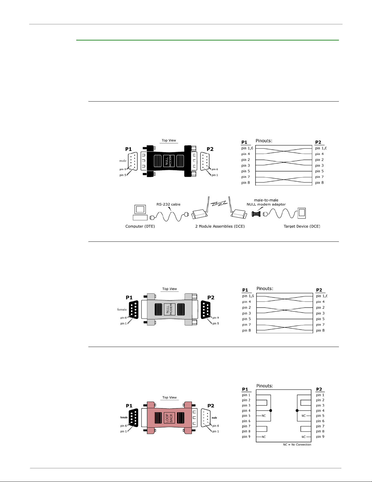
9XTend™ OEM RF Module - Product Manual v2.x6x
Adapters
The development kit includes several adapters that facilitate the following functions:
Performing Range Tests
Testing Cables
Connecting to other RS-232 DCE and DTE devices
Connecting to terminal blocks or RJ-45 (for RS-485/422 devices)
NULL Modem Adapter (male-to-male)
Part Number: JD2D2-CDN-A (Black, DB-9 M-M) The male-to-male NULL modem adapter is
used to connect two DCE devices. A DCE device connects with a straight-through cable to the male
serial port of a computer (DTE).
Figure B-05. Male NULL modem adapter and pinouts
Figure B-06. Example of a Digi Radio Modem (DCE Device) connecting to another DCE device)
NULL Modem Adapter (female-to-female)
Part Number: JD3D3-CDN-A (Gray, DB-9 F-F) The female-to-female NULL modem adapter is
used to verify serial cabling is functioning properly. To test cables, insert the female-to-female
NULL modem adapter in place of a pair of module assemblies (RS-232 interface board + XTend RF
Module) and test the connection without modules in the connection.
Figure B-07. Female NULL modem adapter and pinouts
Serial Loopback Adapter
Part Number: JD2D3-CDL-A (Red, DB-9 M-F) The serial loopback adapter is used for range
testing. During a range test, the serial loopback adapter configures the module to function as a
repeater by looping serial data back into the radio for retransmission.
Figure B-08. Serial loopback adapter and pinouts
© 2010 Digi Internatonal, Inc. 74
Page 75
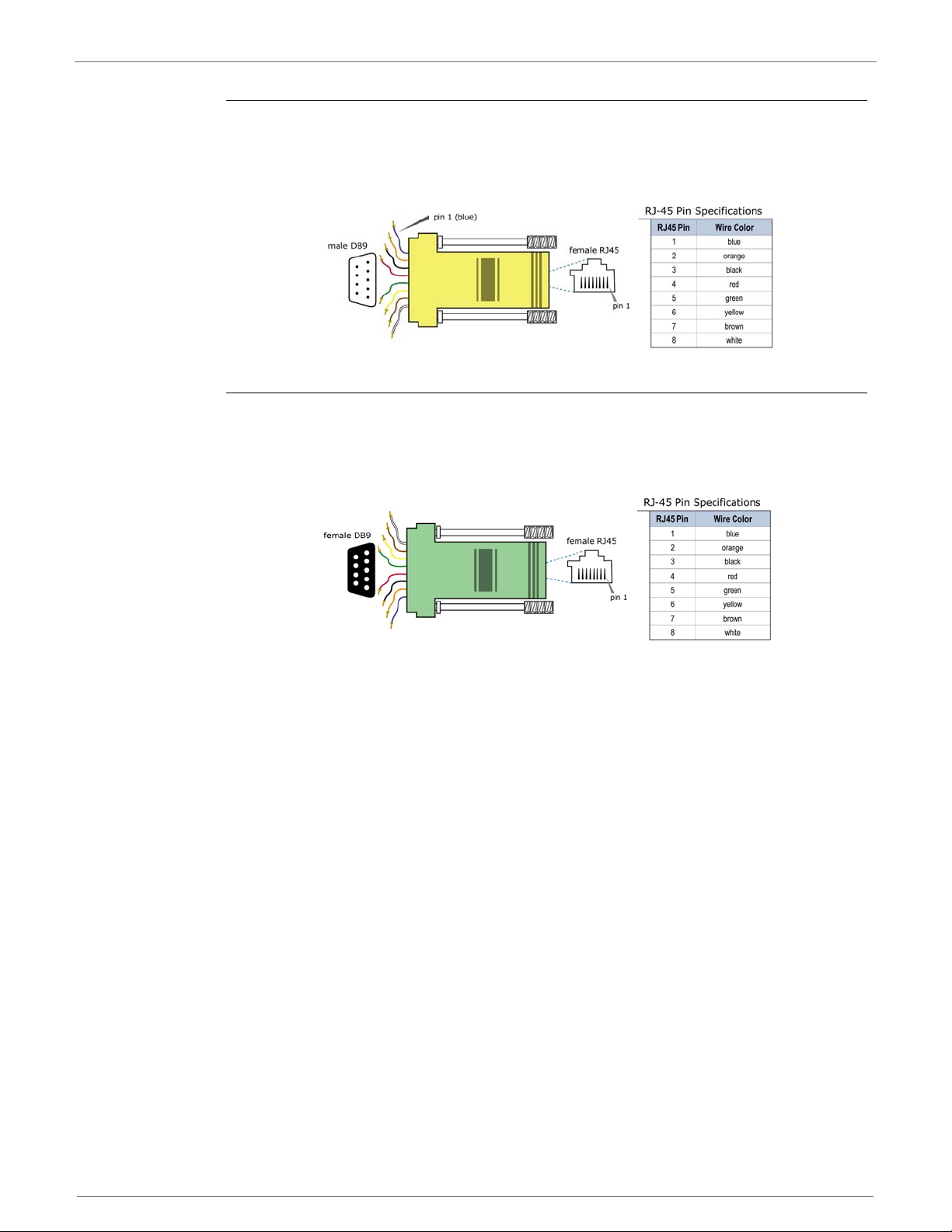
9XTend™ OEM RF Module - Product Manual v2.x6x
Male DB-9 to RJ-45 Adapter
Part Number: JD2D2-CDN-A (Yellow) This adapter facilitates adapting the DB-9 Connector of
the Digi Interface Board to a CAT5 cable (male DB9 to female RJ45).
Refer to the ‘RS-485 (4-wire) & RS-422 Operation’ sections for RS-485/422 connection guidelines.
Figure B-09. Male DB-9 to RJ-45 Adapter and pinouts
Female DB-9 to RJ-45 Adapter
Part Number: JD3D3-CDN-A (Green) This adapter Facilitates adapting the DB-9 Connector of
the Digi Interface Board to a CAT5 cable (female DB9 to female RJ45).
Refer to the ‘RS-485 (4-wire) & RS-422 Operation’ sections for RS-485/422 connection guidelines.
Figure B-10. Female DB-9 to RJ-45 Adapter and pinouts
© 2010 Digi Internatonal, Inc. 75
Page 76

9XTend™ OEM RF Module - Product Manual v2.x6x
Interfacing Protocols
The XTend Module Assembly (XTend OEM RF Module mounted to the XTIB-R Interface Board) supports the following interfacing protocols:
RS-232
RS-485 (2-wire) Half-Duplex
RS-485 (4-wire) and RS-422
RS-232 Operation
DIP Switch Settings and Serial Port Connections
Figure B- erugiF.11 B-12.
RS-232 DIP Switch Seings Pins used on the female RS-232 (DB-9) Serial Connector
DIP Switch seins are read and applied
only while powerin-on.
Table B-04. RS-232 Signals and their implementations on the XTend Module Assembly
DB-9 Pin
* ‘X-CTU’ is soware that can be used to e the module. The soware includes a namin convention
where "GPI" stands for ‘General Purpose Input’ and "GPO" for ‘General Purpose Output’.
(Low-asserted sils are distuished by horizontal line ov
RS-232
Name
1 DCD GPO2 Data-Carrier-Detect Connected to DSR (pin6 of DB-9)
2 RXD DO Received Data Serial data exiting the module assembly (to host)
3 TXD DI Transmitted Data Serial data entering into the module assembly (from host)
4 DTR GPI2 Data-Terminal-Ready Can enable Power-Down on the module assembly
6 DSR GPO2 Data-Set-Ready Connected to DCD (pin1 of DB-9)
7 RTS
8 CTS
9 RI - Ring Indicator
/ CMD GPI1
X-CTU
Name*
GPO1 Clear-to-Send Provides CTS flow control
Description Implementation
Request-to-Send /
Command Mode
Provides RTS flow control or enables Command Mode
Optional power input that is connected internally to the
er pin name.)
dnuorGlangiS dnuorG-DNG5
positive lead of the front power connector
© 2010 Digi Internatonal, Inc. 76
Page 77
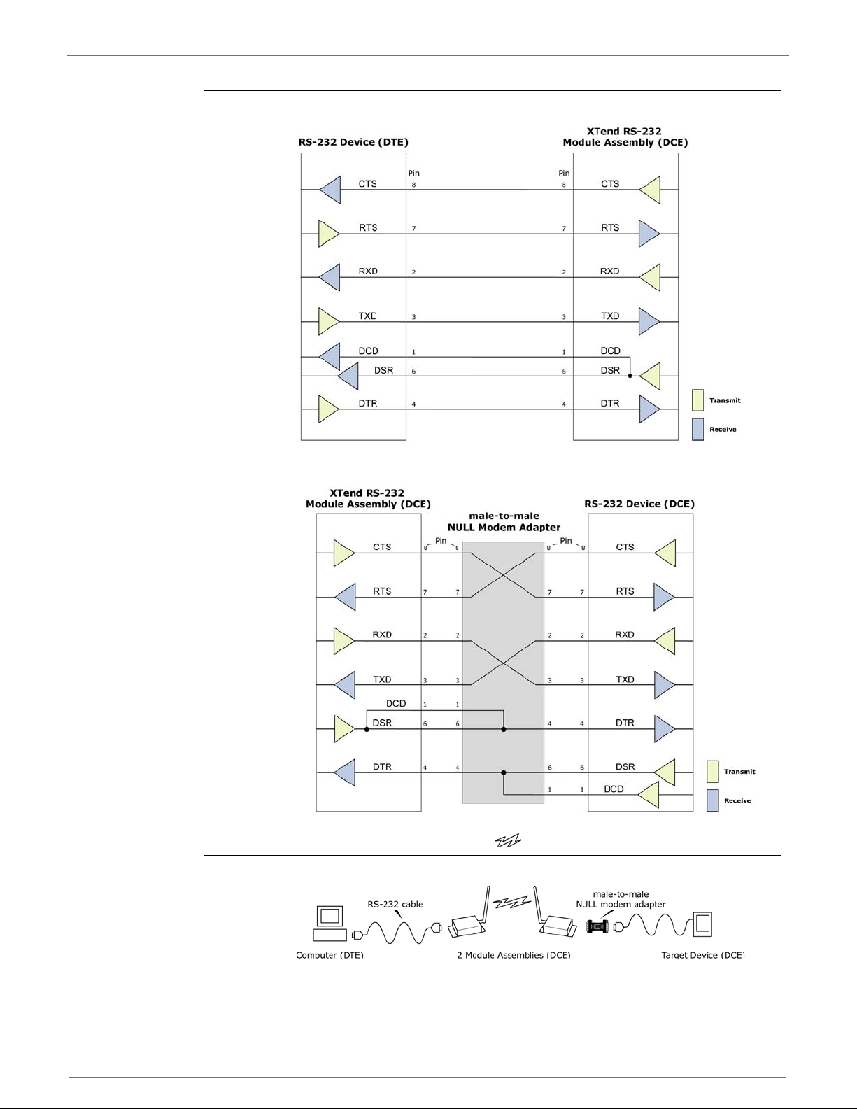
9XTend™ OEM RF Module - Product Manual v2.x6x
Wiring Diagrams
Figure B-13. DTE Device (RS-232, male DB-9 connector) wired to a DCE Module Assembly (female DB-9)
Figure B-14. DCE Module Assembly (female DB-9 connector) wired to a DCE Device (RS-232, male DB-9)
Sample Wireless Connection: DTE <--> DCE DCE <--> DCE
Figure B-15. Typical wireless link between DTE and DCE devices
© 2010 Digi Internatonal, Inc. 77
Page 78
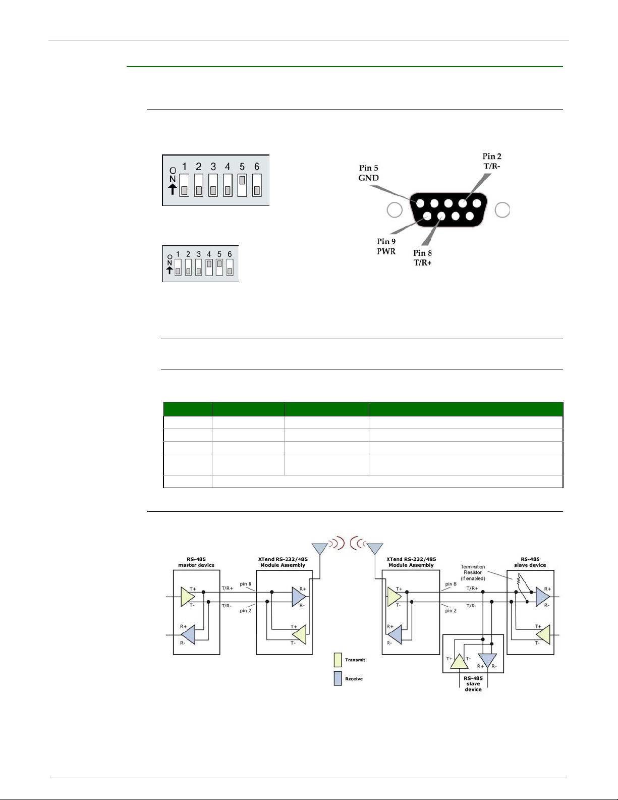
9XTend™ OEM RF Module - Product Manual v2.x6x
RS-485 (2-wire) Operation
When operating within the RS-485 protocols, all communications are half-duplex.
DIP Switch Settings and Serial Port Connections
Figure B- erugiF.61 B-17.
RS-485 (2-wire) Half-duplex Pins used on the female RS-232 (DB-9)
DIP Switch laireSsgnitteS Connector
Figure B-18.
RS-485 (2-wire) w/ Termination (optional)
Termination is the 120 resistor between T+ and T-.
DIP Switch seings are read and applied only while powering-on.
Note: Refer to Figures B-09 and B-10 for RJ-45 connector pin designations used in
RS-485/422 environments.
Table B-05. RS-485 (2-wire half-duplex) signals and their implementations on the XTend Module Assembly
DB-9 Pin RS-485 Name Description Implementation
2 T/R- (TRA) Negative Data Line Transmit serial data to and from the XTend Module Assembly
dnuorGlangiS dnuorGDNG5
8 T/R+ (TRB) Positive Data Line Transmit serial data to and from the XTend Module Assembly
9 PWR Power
Wiring Diagram
Figure B-19. XTend Module Assembly in an RS-485 (2-wire) half-duplex environment
Optional power input that is connected internally
to the front power connector
desu ton7 ,6 ,4 ,3 ,1
© 2010 Digi Internatonal, Inc. 78
Page 79

9XTend™ OEM RF Module - Product Manual v2.x6x
RS-485 (4-wire) & RS-422 Operation
DIP Switch Settings and Serial Port Connections
Figure B- erugiF.02 B-21.
RS-485 (4-wire) & RS-422 Pins used on the female RS-232 (DB-9)
DIP Switch laireSsgnitteS Connector
Figure B-22.
RS-485 (4-wire)& RS-422 w/ Termination (optional)
Termination is the 120 resistor between T+ and T-.
DIP Switch seings are read and applied only while powering-on.
Note: Refer to Figures B-09 and B-10 for RJ-45 connector pin designations used in
RS-485/422 environments.
Table B-06. RS-485/422 (4-wire) Signals and their implementations on the XTend Module Assembly
DB-9 Pin
2T- (TA)
3R- (RA)
7 R+ (RB)
8 T+ (TB)
9 PWR Power
RS-485/422
Name
Description Implementation
Transmit Negative
Data Line
Receive Negative
Data Line
Receive Positive
Data Line
Transmit Positive
Data Line
Serial data sent from the XTend Module Assembly
Serial data received by the XTend Module Assembly
dnuorGdnuorG langiSDNG5
Serial data received by the XTend Module Assembly
Serial data sent from the XTend Module Assembly
Optional power input that is connected internally
to the front power connector
desu ton6 ,4 ,1
© 2010 Digi Internatonal, Inc. 79
Page 80
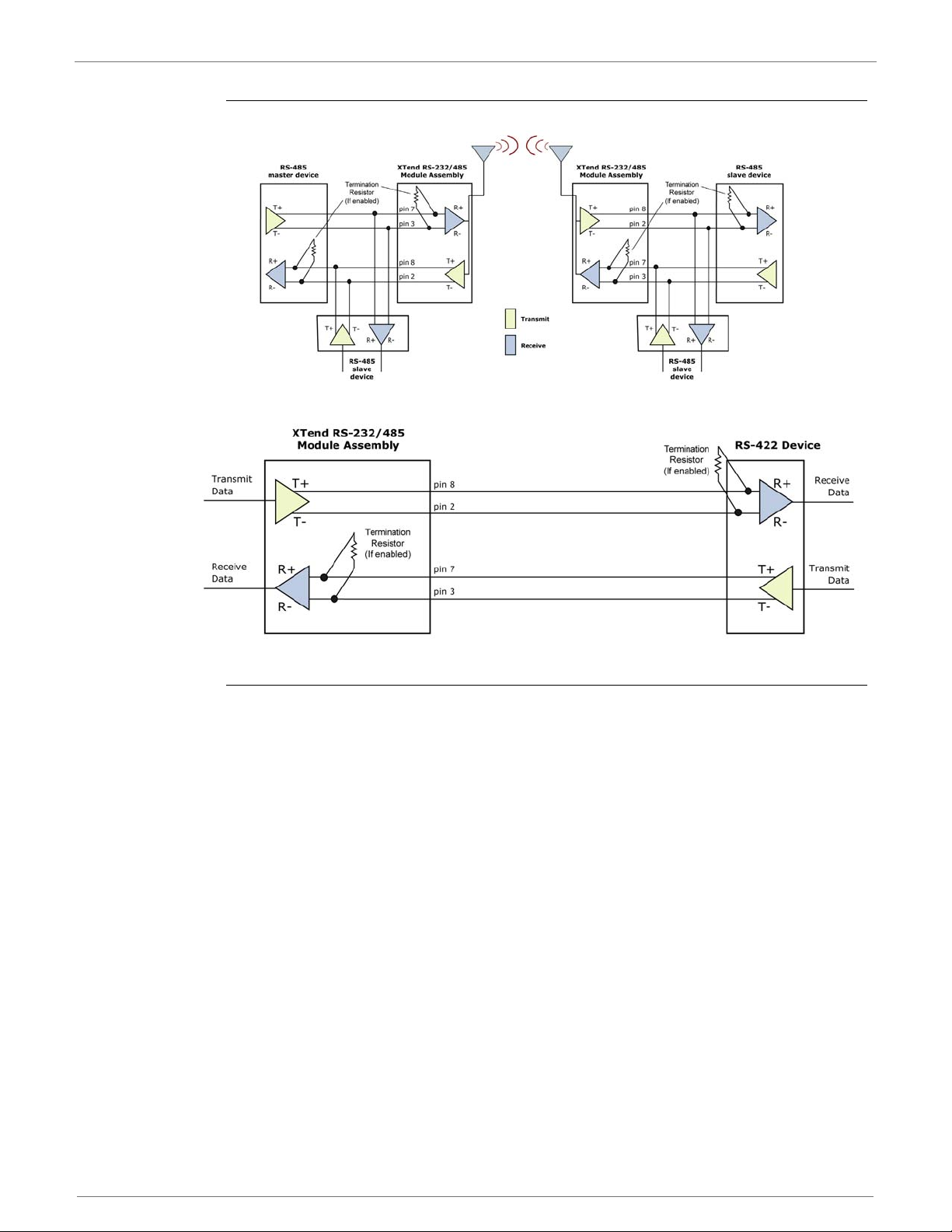
9XTend™ OEM RF Module - Product Manual v2.x6x
Wiring Diagrams
Figure B-23. XTend Module Assembly in an RS-485 (4-wire) environment
Figure B-24. XTend Module Assembly in an RS-422 environment
RS-485/422 Connection Guidelines
The RS-485/422 protocol provides a solution for wired communications that can tolerate high
noise and push signals over long cable lengths. RS-485/422 signals can communicate as far as
4000 feet (1200 m). RS-232 signals are suitable for cable distances up to 100 feet (30.5 m).
RS-485 offers multi-drop capability in which up to 32 nodes can be connected. The RS-422 protocol is used for point-to-point communications.
Suggestions for integrating the XTend RF Module with the RS-485/422 protocol:
1. When using Ethernet twisted pair cabl
each wire in a twisted pair. Likewise, select wires so that R+ and R- are connected to a
twisted pair. (For example, tie the green and white/green wires to T+ and T-.)
2. For straight-through Ethernet cable (not cross-over cable) - The following wiring pattern
works well: Pin3 to T+, Pin4 to R+, Pin5 to R-, Pin6 to T-
3. Note that the connecting cable only requires 4 wires (even though there are 8 wires).
4. When using phone cabling (RJ-11) - Pin2 in the cable maps to Pin3 on opposite end
cable and Pin1 maps to Pin4 respectively.
ing: Select wires so that T+ and T- are connected to
of
© 2010 Digi Internatonal, Inc. 80
Page 81
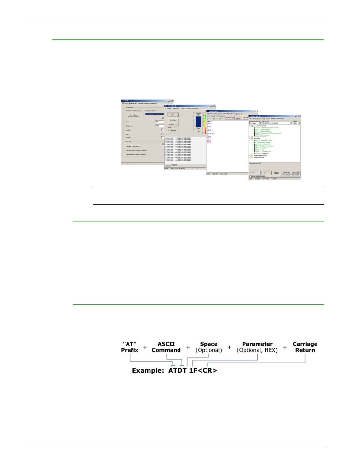
9XTend™ OEM RF Module - Product Manual v2.x6x
X-CTU Software
X-CTU is a Digi-provided software program used to interface with and configure Digi RF Modules.
The software application is organized into the following four tabs:
PC Settings tab - Setup PC serial ports for interfacing with an RF module
Range Test tab - Test the RF module's range and monitor packets sent and received
Terminal tab - Set and read RF module parameters using AT Commands
Modem Configuration tab - Set and read RF module parameters
Figure B-11. X-CTU User Interface (PC Seings, Range Test, Terminal and Modem guration tabs)
NOTE: PC Setting values are visible at the bottom of the Range Test, Terminal and Modem Configuration tabs. A shortcut for editing PC Setting values is available by clicking on any of the values.
Installation
Double-click the "setup_X-CTU.exe" file and follow prompts of the installation screens. This file is
located in the 'software' folder of the Digi CD and also under the 'Downloads' section of the following web page: www.maxstream.net/support/downloads.php
Setup
To use the X-CTU software, a module assembly (An RF module mounted to an interface Board)
must be connected to a serial port of a PC.
NOTE: Failure to enter AT Command Mode is most commonly due to baud rate mismatch. The
interface data rate and parity settings of the serial port ("PC Settings" tab) must match those of
the module (BD (Baud Rate) and NB (Parity) parameters respectively).
Serial Communications Software
A terminal program is built into the X-CTU Software. Other terminal programs such as "HyperTerminal" can also be used to configure modules and monitor communications. When issuing AT Commands through a terminal program interface, use the following syntax:
Figure B-12. Syntax for sending AT Commands
NOTE: To read a parameter value stored in a register, leave the parameter field blank.
The example above issues the DT (Destination Address) command to change destination address
of the module to "0x1F".
(Write) command after modifying parameters.
To save the new value to the module’s non-volatile memory, issue WR
© 2010 Digi Internatonal, Inc. 81
Page 82

Appendix C: Additional Information
1-Year Warranty
WARRANTY PERIOD: Digi warranties hardware Product for a period of one (1) year.
WARRANTY PROCEDURE: Upon return of the hardware Product Digi will, at its option, repair or
replace Product at no additional charge, freight prepaid, except as set forth below. Repair parts
and replacement Product will be furnished on an exchange basis and will be either reconditioned or
new. All replaced Product and parts become the property of Digi. If Digi determines that the Product is not under warranty, it will, at the Customers option, repair the Product using current Digi
standard rates for parts and
warranty.
Ordering Information
Figure C-01. Divisions of the XTend RF Module Part Numbers
labor, and return the Product FedEx Ground at no charge in or out of
For example:
XT09-SI = 9XTend OEM RF Module, 900 MHz, RPSMA Antenna, Industrial Temperature Rating
© 2010 Digi International Inc. 82
Page 83

9XTend™ OEM RF Module - Product Manual v2.x6x
Contact MaxStream
For the best in wireless data solutions and support, please use the following resources:
Documentation: www.maxstream.net/support/downloads.php
Technical Support: Phone. (866) 765-9885 toll-free U.S.A. & Canada
Office hours are 8:00 am - 5:00 pm [U.S. Mountain Standard Time]
(801) 765-9885 Worldwide
Live Chat. www.digi.com
/moc.igid.www//:ptth:troppus-E support/eservice/eservicelo-
gin.jsp
© 2010 MaxStream, Inc. 83
 Loading...