

Page 1
9XCite™ Wireless OEM Module
9XCite Wireless OEM Module
RF System Components
Module Configuration
Appendices
Product Manual v1.0
For 9XCite Module Part Numbers: XC09-009…
XC09-038…
355 South 520 West, Suite 180
Lindon, UT 84042
Phone: (801) 765-9885
Fax: (801) 765-9895
support@MaxStream.net
www.MaxStream.net
M100043
12.02.2003
Page 2

XCite Wireless OEM Module – Product Manual v1.0
© 2003 MaxStream, Inc. All rights reserved
No part of the contents of this manual may be transmitted or
reproduced in any form or by any means without the written
permission of MaxStream, Inc.
9XCite™ is a trademark of MaxStream, Inc.
Phone: (801) 765-9885
Live Chat: www.maxstream.net
E-Mail: support@maxstream.net
© 2003 MaxStream, Inc., Confidential and Proprietary
ii
Page 3

Contents
9XCite Wireless OEM Module 1
Powerfully Simple 1
Block Diagram 2
Module Pinout Signals 2
Timing Specifications 4
Mechanical Drawings 5
Electrical Characteristics 5
RF System Components 6
Serial Communications 6
UART-Interfaced Data Flow 6
RS-232 and RS-485/422 Data Flow 6
Interfacing Hardware 7
9XCite Development Kit 7
MaxStream Interface Board (Part Number: XIB-R) 7
MaxStream Interface Board Components & Features 8
XCite Wireless OEM Module – Product Manual v1.0
Module Configuration 9
Command & Parameter Types 9
XCite Commands & Parameter Reference 10
Configuration Software 12
XCite-CTU Software 12
Serial Communications Software (for AT Commands Only) 12
Appendix A: FCC Certification 13
9XCite (900 MHz) Module - FCC Compliance 13
OEM Labeling Requirements 13
FCC Notice 14
9XCite (900 MHz) Approved Antenna List 15
Appendix B: Specifications 16
9XCite Wireless OEM Module Specifications 16
Appendix C: Additional Information 17
1-Year Warranty 17
9XCite Wireless OEM Module Part Numbers 18
Appendix D: Troubleshooting & FAQs 19
Contact MaxStream 19
© 2003 MaxStream, Inc., Confidential and Proprietary
iii
Page 4

9XCite Wireless OEM Module – Product Manual v1.0
9XCite
Wireless OEM Module
Powerfully Simple
The 9XCite Module is a drop-in wireless solution that adds connectivity to any UART or serial
device. It transfers a standard asynchronous serial data stream and features the following:
• Continuous data stream of up to 38400 bps (factory-set, over-the-air baud rate)
• Serial Interfacing from 1200 to 57600 bps
• Software selectable between Hopping (FHSS) and Single Channel modes
• Approved by the FCC under Part 15 of the FCC Rules and Regulations
• Variable input supply voltage (2.85 – 5.50 VDC)
This manual contains information critical to basic 9XCite Module operation. More detailed
information is available in the “XCite Advanced Programming & Configuration” Manual. (Located
on the MaxStream CD or on the web: www.maxstream.net/support_documentation.html
)
Features:
FCC Approved (USA) [Go to Appendix A for FCC Requirements]
Devices that embed 9XCite Modules inherit MaxStream’s FCC certification.
IC (Industry Canada) Certified
ISM (Industrial, Scientific & Medical) frequency band
MaxStream products manufactured under ISO 9002 registered standards since 2000.
Indoor/Urban Range: Up to 300’ (90 m)
Outdoor/LOS Range: Up to 1000’ (300 m) w/dipole antenna
Receiver Sensitivity: -108 dBm (9600 Baud), -104 dBm (38400 Baud)
Transmit Power Output: 1 mW
Advanced Networking capabilities (True Peer-to-Peer (no “master” required), Point-to-Point,
Point-to-Multipoint, Multi-Drop)
Specifications [Appendix B]
1-Year Warranty [Appendix C]
Free Technical Support [Appendix D]
[50 mW effective considering excellent receiver sensitivity]
© 2003 MaxStream, Inc., Confidential and Proprietary 1
Page 5
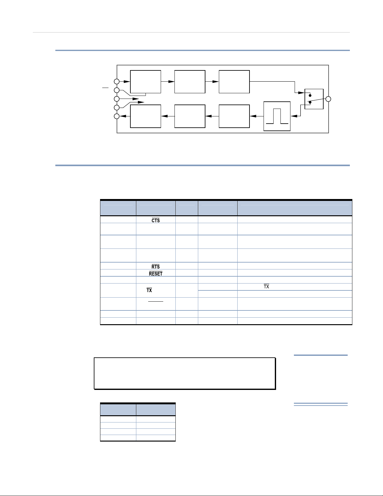
Block Diagram
Figure 1. 9XCite Module Block Diagram
9XCite Wireless OEM Module – Product Manual v1.0
DIN
CTS
VCC
GND
DOUT
DIN Buffer
DOUT Buffer
RF TX Buffer
RF RX Buffer
‘Interference Filter’ reduces interference from pagers and cellular.
Module Pinout Signals
9XCite Module pin signals and their functions:
Table 1. J1 Pin Descriptions
(Low-asserted signals distinguished with a horizontal line over signal name.)
Module Pin Signal Name I/O When Active Description
1
2
SLEEP
(PWRDN)
3 DO (Data Out)
4 DI (Data In)
5
6
7 RX LED
8
9
/ PWR
CONFIG
10 VCC
11 GND
* Pin utilizes 10K Ω Pull-Up resistor (Already installed in the module)
** Pin utilizes 10K Ω Pull-Down resistor (Already installed in the module)
*** Pin utilizes 100K Ω Pull-Up resistor (Already installed in the module)
Note When integrating the 9XCite Module onto a Host PC
Board, all lines that are not used should be left
disconnected (floating).
Table 2. J2 Pin Descriptions
O* low Clear-to-Send Flow Control
O* n/a
I** low Request-to-Send
I*** low
Transmitting
Circuitry
Receiving
Circuitry
Interference
Filter
RF Switch
I* high Can be used to enter Sleep Mode
Serial Data leaving the 9XCite Module
(to the processor host)
I n/a
Serial Data entering the 9XCite Module
(from the processor host)
I* low Reset module
O high Receive LED
O
low - Asserted during transmission
high PWR – Indicates power is on
Backup method for entering Command Mode. Primary
method is with “+++” [See CC Parameter]
I - 2.85 – 5.50 VDC variable
- - Ground
For More Information
Go to the "XCite Advanced
Programming & Configuration"
Manual for more detailed
information about
module signal pinouts.
The advanced manual is available
on the MaxStream CD
or on the web:
www.MaxStream.net
Antenna
Port
Module Pin Pin Name
1 reserved
2 GND
3 GND
4 GND
J2 Pins are used primarily for mechanical stability and may be left disconnected.
© 2003 MaxStream, Inc., Confidential and Proprietary 2
Page 6

9XCite Wireless OEM Module – Product Manual v1.0
Pinout Signal Overview
The interface signals are available through the 11-pin header. All pins operate on VCC CMOS
levels. Five signals that are commonly used in applications are:
• DI (pin 4 – Data In)
• DO (pin 3 – Data Out)
• VCC (pin 10 – Power)
• GND (pin 11 – Ground)
•
The remaining 6 pins (SLEEP (PWRDN),
additional functionality. Go to the “XCite Advanced Programming & Configuration Manual” for
more detailed information about module pinouts.
(pin 1 – Clear-to-Send)
, , RX LED, /PWR, ) may be used for
Application Circuit
Figure 2. Application Circuit – connection to host processor
Serial Data
Data enters the 9XCite Module through the DI Pin as an asynchronous serial signal. The signal
should idle high when no data is being transmitted.
Each data packet consists of a start bit (low), 8 data bits (least significant bit first) and a stop bit
(high). The following figure illustrates the serial bit pattern of data passing through the module.
Figure 3. UART data packet 0x1F (decimal number “31”) as transmitted through the 9XCite Module
The 9XCite Modules transfer 7 or 8 bits over-the-air [Selectable using BI Parameter]. The start
and stop bits from the UART signal are not transmitted, but are regenerated on the receiving
module.
DI (Data In) Buffer
Once serial data has entered the 9XCite Module through the Data In (DI) Pin, the data is stored
in the DI Buffer until it can be transmitted.
Once the first byte of data enters the DI Buffer, the module begins to initialize the RF channel
(unless RF data is being received). In the case where the module is receiving RF data, the serial
data is stored in the DI Buffer. When the DI Buffer has only 17 bytes of memory left, the 9XCite
Module de-asserts (high)
once the DI Buffer has at least 35 bytes available in memory. Once in the DI Buffer, the data is
packetized for transmission. [The packet structure is broken down on the next page.]
to signal to the host device to stop sending data. re-asserts
© 2003 MaxStream, Inc., Confidential and Proprietary 3
Page 7
9XCite Wireless OEM Module – Product Manual v1.0
<VID><ATHP><ATDT><PSN><Pay Load><CRC>
<VID> Factory assigned Vendor ID number
<ATHP> Channel (or Network) number
<ATDT> Module Address
<PSN> Packet Serial Number (8-bit number that uniquely identifies each packet)
<Pay Load> Data shifted into module for transmission
<CRC> 16-bit CRC (like a checksum) for error detection
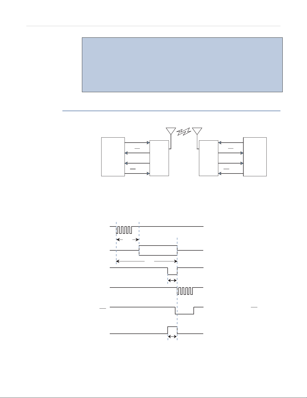
Timing Specifications
The diagram below [Figure 4] shows 9XCite Modules providing an RF Link between hosts.
Figure 4. System Block Diagram
HOST A
DI (data in)
CTS
DO (data out)
XCite
Module A
XCite
Module B
DI (data in)
CTS
DO (data out)
HOST B
RTS / CMD
RTS / CMD
The RF data flow sequence is initiated when the first byte of data is received by the transmitting
9XCite Module. As long as 9XCite Module A is not already receiving data, the serial data goes into
the DI Buffer, is packetized and then transmitted to 9XCite Module B.
Figure 5. Timing Specifications (“A” and “B” are associated with figure 4)
D A
IN
RF A
OUT
TXLED A
D B
OUT
T
ST
A Transmits over air
B Receives
T
TX
T
TL
Host A sends serial data to XStream Module A
After 1st byte is received, contents of D Buffer
are assembled into packet and transmitted
IN
TX/PWR LED on XStream Module A pulses off
briefly to indicate RF transmission
If 16-bit CRC checks out, data is shifted out
serial port to Host B
CTS B
(Optional) Set ATCS = 1 to use CTS as RS-485
TX enable low-asserted signal
RXLED B
T
RL
RXLED pulses on briefly to indicated RF receive
activity
© 2003 MaxStream, Inc., Confidential and Proprietary 4
Page 8

Mechanical Drawings
Figure 6. Mechanical Drawings (Measures are in inches)
9XCite Wireless OEM Module – Product Manual v1.0
Electrical Characteristics
Table 3. DC Characteristics (Vcc = 2.85 to 5.50V)
Symbol Parameter Condition Min Typical Max Units
VIL Input Low Voltage All Input Signals -0.5 0.3 * Vcc V
VIH Input High Voltage
V
Input High Voltage Pin * 0.9 * Vcc Vcc + 0.5 V
IH2
VOL Output Low Voltage
VOH Output High Voltage
IIL
IIH
I
, DO, (Vcc – VI)/10 ** mA
IL2
I
(Vcc – VI)/47 ** mA
IL3
I
(Vcc – VI)/10 ** mA
IH2
Input Leakage
Current I/O Pin
Input Leakage
Current I/O Pin
All Except
Pin
= 20 mA,
I
OL
Vcc = 5V
= -20 mA,
I
OH
Vcc = 5V
Vcc = 5.5V, pin low (absolute
value)
Vcc = 5.5V, pin high (absolute
value)
0.6 * Vcc Vcc + 0.5 V
0.7 V
4.0 V
3 µA
3 µA
* Reset pulse must last at least 250 nanoseconds
I = the input voltage on the pin
** V
© 2003 MaxStream, Inc., Confidential and Proprietary 5
Page 9

9XCite Wireless OEM Module – Product Manual v1.0
RF System Components
Serial Communications
The 9XCite Wireless OEM Module interfaces to a host device through a CMOS-level asynchronous
serial port. Through its serial port, the 9XCite Module can communicate directly with any UART-
interfaced or RS-232/485/422 device. [Timing specifications illustrated on page 4]
UART-Interfaced Data Flow
Devices that have a UART interface can connect directly through the pins of the 9XCite Wireless
OEM Module as is shown in the figure below.
Figure 7. Data Flow in a UART-interfaced environment
(Low-asserted signals distinguished with horizontal line over signal name.)
Microcontroller
CMOS Logic CMOS Logic
DI (data in)
CTS
DO (data out)
RTS
XCite
Module
XCite
Module
DI (data in)
CTS
DO (data out)
RTS
Microcontroller
RS-232 and RS-485/422 Data Flow
Wiring the 9XCite Module to a host device serial port enables the host device to communicate
wirelessly. To transmit, the host device simply sends serial data to the 9XCite Module pins. The
9XCite Module then converts the data to Frequency Hopping Spread Spectrum (FHSS) or Single
Channel FCC-approved wireless data. Once transmitted, the over-the-air data can be detected by
receiving 9XCite Modules, checked for integrity and then sent to a receiving device [Figure
below].
Figure 8. Data Flow in RS-232 and RS-485/422 environments.
(Low-asserted signals distinguished with a horizontal line over signal name.)
RS-232 Logic CMOS Logic RS-232 Logic
PC
TX
CTS
RX
RTS
MaxStream
Interface
Board
© 2003 MaxStream, Inc., Confidential and Proprietary 6
CMOS Logic
DI (data in)
CTS
DO (data out)
RTS
XCite
Module
XCite
Module
DI (data in)
CTS
RTS
MaxStream
Interface
Board
TX
CTS
RXDO (data out)
RTS
PC
Page 10

Interfacing Hardware
MaxStream, Inc. developed a proprietary interface board (MaxStream Product number: XIB-R) to
facilitate the connection between 9XCite Wireless OEM Modules and serial devices. Many
integrators develop their own interfacing circuitry; others use MaxStream’s XIB-R Interface
Board. In either case, the following sections illustrate how to interface with 9XCite Wireless OEM
Modules by illustrating properties of the MaxStream XIB-R Interface Board.
9XCite Development Kit
The MaxStream Interface board is included with the 9XCite Development Kit. The kit includes all
the hardware and software needed for basic wireless connections.
Table 4. 9XCite Development Kit contents
Item Qty. Description Part Number
9XCite Wireless OEM Module – Product Manual v1.0
9XCite Module
(w/ RPSMA connector)
9XCite Module
(w/ wire antenna)
MaxStream Interface
Board
Antenna 1 RPSMA half-wave dipole antenna. A09-HASM-675
Quick Start Guide 1
CD 1 CD includes documentation and configuration software MD0010
Serial Loopback Adapter 1
NULL Modem Adapter
(male-to-male)
NULL Modem Adapter
(female-to-female)
Male DB-9 to RJ-45
Adapter
Female DB-9 to RJ-45
Adapter
9V DC Power Adapter 2 Allows Interface Board to be powered by a 110 Volt AC power supply JP4P2-9V4-6F
9V Battery Clip 1 Allows Interface Board to be remotely powered by a 9V battery JP2P3-C2C-4I
RS-232 Cable (6’) 2 Connects interface board to devices having an RS-232 serial port JD2D3-CDS-6F
1 Module comes with fixed over the air baud rates up to 38400 bps XC09-…-NSC
1 Modules comes with fixed over the air baud rates up to 38400 bps XC09-…-WNC
2 Enables interfacing to RS-232/485/422 devices XIB-R
Quickly familiarize users with some of the 9XCite Module’s most
important functions. The guide provides step-by-step instructions on
how to make a wireless connection and test its ability to transport data
over varying ranges and conditions.
Connects to the female RS-232 (DB-9) serial connector of the 9XCite
Module and can be used to configure the radio modem to function as a
repeater (for range testing)
Connects to the female RS-232 (DB-9) serial connector of the 9XCite
1
Module and can be used to connect the radio modem to another DCE
(female DB9) device
1 Used to bypass radios to verify serial cabling is functioning properly JD3D3-CDN-A
Facilitates adapting the DB-9 Connector to a CAT5 cable
1
(female RJ45 to male DB9)
Facilitates adapting the DB-9 Connector to a CAT5 cable
1
(female RJ45 to female DB9)
MD0009
JD2D3-CDL-A
JD2D2-CDN-A
JE1D2-CDA-A
JE1D3-CDA-A
MaxStream Interface Board (Part Number: XIB-R)
The MaxStream Interface board was developed to provide a means of connecting the 9XCite
Module to any system having an RS-232 or RS-485/422 connection. Since the 9XCite Module
requires signals to enter at CMOS voltages, one of the main functions of the interface board is to
convert interface signals between CMOS levels (2.85 – 5.50V) and RS-232 levels (-12 - +12V).
The MaxStream Interface Board includes the following built-in features:
• DIP Switch
• Configuration Switch
• Power Switch
• LEDs
• DB-9 Connector
• Power Connector
© 2003 MaxStream, Inc., Confidential and Proprietary 7
Page 11

9XCite Wireless OEM Module – Product Manual v1.0
MaxStream Interface Board Components & Features
9a. Power Switch
Move the Power Switch to the on (up) position to power the
Interface Board. DIP Switch [10a] settings are only read during a
power-up sequence.
9b. LEDs
The LED indicators visualize diagnostic status information. The
radio modem’s status is represented as follows:
Yellow (top LED) = Serial Data Out
Green (middle) = Serial Data In
Red (bottom) = Power/TX Indicator
9c. DB—9 Connector
Standard female DB-9 (RS-232) DCE connector – This connector
can be also used for RS-485 and RS-422 connections.
9d. Power Connector
7-18 VDC Power Connector (Center positive, 5.5/2.1mm) – Power
can also be supplied through Pin 9 of the DB-9 Connector.
(Red light is on when powered,
off briefly during RF transmission)
10a. DIP Switch
Figure 11. MaxStream Interface Board DIP Switch Settings
The DIP Switch configures the 9XCite OEM Module to operate in
different modes. DIP Switch settings are only read and
applied during a powering-on sequence. [See Figure 11 below
for DIP Switch settings]
10b. Configuration Switch
The Configuration Switch provides an alternate way to enter “AT
Command Mode”. To enter “AT Command Mode” at the radio
modem’s default baud rate, hold the Configuration Switch down
while powering on the module using the Power Switch.
* The “Restore Defaults” setting, for switches 1 & 2, can be used to restore AT Settable parameters to their default states. Once switches are in position, reset occurs
during next power- up
© 2003 MaxStream, Inc., Confidential and Proprietary 8
Page 12

9XCite Wireless OEM Module – Product Manual v1.0
Module Configuration
The following versions of the 9XCite Module are currently available:
• 900 MHz, 9600 (over-the-air) Baud, Hopping Channel Mode
• 900 MHz, 9600 Baud, Single Channel mode
• 900 MHz, 38400 Baud, Hopping Channel mode
• 900 MHz, 38400 Baud, Single Channel mode
9XCite Modules can operate in both Single Channel and Hopping
modes. Mode is selectable using the “Function Set” dropdown list of
the “XCite Configuration” tab of the MaxStream-provided XCite-CTU Software.
The 9XCite Module is shipped with a unique parameter set in its memory. Parameters within the
set are organized under the following three categories: AT Commands, Non-AT Settable
Parameters and Read-Only AT Commands.
Command & Parameter Types
AT Commands
AT Commands can be changed at any time by entering AT Command Mode and sending
commands to the module.
AT Commands can be modified using the any of the following means:
• XCite-CTU Software
• Serial Communications Software (“HyperTerminal”, “Pro Comm”, etc.)
• Microcontroller
For More Information
Go to the "XCite Advanced
Programming & Configuration"
Manual for more detailed
information about
module configurations.
The advanced manual is available
on the MaxStream CD
or on the web:
www.MaxStream.net)
Non-AT Settable Parameters (XCite-CTU Software configurable only)
Non-AT Settable Parameters can only be adjusted using the MaxStream-provided XCite-CTU
Software. To modify Non-AT Settable Parameter, connect the module to the serial com port of a
PC (interface board is necessary for RS-232 connection) and modify parameter values through
the XCite-CTU Software interface. These parameters enable features that need to be set before
the module is used in the field. [Non-AT Settable Parameters are listed in table 7.]
Non-AT Settable Parameters can be modified using the following means:
• XCite-CTU Software (MaxStream-provided)
© 2003 MaxStream, Inc., Confidential and Proprietary 9
Page 13

9XCite Wireless OEM Module – Product Manual v1.0
XCite Commands & Parameter Reference
XCite AT Commands and Non-AT Settable Parameters are organized under the following
categories:
• AT Command Mode Options
• Diagnostic
• Networking
• Serial Interfacing
• Sleep Mode (Low Power)
Table 5. AT Commands
(Settable/Readable using XCite-CTU Software, Serial Communications Software or Microcontroller)
Command
Category
(Special) WR
AT Command
Mode
Options
Diagnostic
Networking
Serial
Interfacing
Options
AT
Command
HV
SH
SL Serial Low – Reads and returns the module serial number low word. Read-Only 2 none
VR
DB
RE
DT
HP
MK
CD RX LED I/O – Redefines the RX LED I/O line.
CS RS-485 Transmit Enable – Modifies behavior of the
Command Description Parameters
Write – Writes all configurable parameters to non-volatile memory.
All AT Command Settable Parameters are stored.
Hardware Version – Reads and returns the hardware version of the
9XCite Module.
Serial High – Reads and returns the module serial number high
word.
Firmware Version – Reads and returns the firmware version of the
9XCite Module.
Receive Signal Strength (Decibels) – Returns the signal strength
(in decibels) of the last received packet.
Default Configuration – Restores module’s default configuration
(Only AT Command Settable Parameter defaults)
Module Address – Sets local module address. Only modules with
the same address can communicate with each other.
Channel - Adjusts the module’s channel number to allow the module
to hop on a specific hopping sequence. This allows independent
networks of modules to operate in the same vicinity.
Address Mask – Sets global address mask. A global address is one
that has the same bits set as the Address Mask. This can be used to
allow a base module to receive data from a range of addresses. It
may also be used to configure “subnets” of modules that
communicate in a group.
signal.
None n/a none
Read-Only 2 none
Read-Only 2 none
Read-Only 2 none
Read-Only 1 none
None n/a none
Range: 0x00 - 0xFFFF
Hopping Channel Mode Range:
0 – 6
Single Channel Mode Range:
0x00 - 0x18 (Decimal: 0 – 24)
Range: 0x00 - 0xFFFF 2 0xFFFF
Range: 0 – 5
0 = RX LED
1 = high
2 = low
3 = input
4 = output
5 = carrier detect
Range: 0 – 4
0 = Normal
1 = RS-485 enable low
2 =
3 = RS-485 enable high
4 =
high
low
# Bytes
Returned
1 0
2 0
1 0
1 0
Factory
Default
© 2003 MaxStream, Inc., Confidential and Proprietary 10
Page 14

Table 6. Non-AT Settable Parameters
(Settable using XCite-CTU Software only)
9XCite Wireless OEM Module – Product Manual v1.0
Command
Category
AT Command
Equivalent
AT
BT
AT Command
Options
CC
CT
Networking ID
BD
BI
FL
Serial
Interfacing
Options
NB
RT Mode – Enables Mode.
SB Stop Bits – Sets number of stop bits.
HT
LH
PW Pin Wake Up – Allow s pin wake up from Cyclic Sleep Mode.
Sleep
(Low Power)
SM Sleep Mode – Specifies Sleep Mode settings.
ST
Command Description Parameter Range
Silence AFTER Sequence - Sets time period of silence after
a command sequence.
Silence BEFORE Sequence – Sets period of silence time
before a command sequence.
Commands Sequence Character –Parameter determines
ASCII command sequence character used to enter AT
Command Mode.
Time Out from Command Mode – If no valid commands
have been received within this time period, module returns to
Idle Mode from AT Command Mode.
Assign Module VID – Sets Module VID for creating separate
networks.
Baud Rate – Sets serial com port’s baud rate (bps) and thus
sets the rate at which serial data enters into the module.
If Com Port Baud rate is set higher than the fixed over-the-air
baud of the module,
Number of Bits (7 or 8) – Sets number of data bits per
character (Bits between start and stop bits).
Software Flow Control – Enables serial software flow control
on the module. (Hardware flow control (
XON = 0x11, XOFF = 0x13
Parity – Sets error-checking parameters for parity systems.
Setting 7 bits (using BI Parameter) and Mark or Space parity
will result in a setting of 7 bits and no parity.
Time-to-Beacon – Sets time of inactivity (no serial or RF data
sent or received) before a wake-up beacon is transmitted.
Value should be shorter than time set with ST Command.
Beacon Transmit Time – Specifies the length of the wake-up
beacon. The length of the beacon should be longer than the
interval if time set using SM Command.
Time-to-Sleep – Sets the time of inactivity before entering
Sleep Mode. (This number is only valid with SM Command
Cyclic and Serial Port Sleep settings.)
may need to be implemented.
) is always on.)
Range: 0x00 - 0xFFFF
(milliseconds)
Range: 0x00 - 0xFFFF
(milliseconds)
# Bytes
Returned
2 0x1F4
2 0x1F4
Factory
Default
0x2B
Range: 0x20 – 0x7F 1
(plus sign “+”
in ASCII.)
Range: 0x02 – 0xFFFF
(tenths of a second)
2 0xC8
Range: 0x00 - 0x3332 1 0x3332
Range: 0 – 6
(1200 – 57600 BPS)
1
Set to equal
module’s
over-the-air
Baud rate.
Range: 0 – 1
0 = 7 bits
1 1
1 = 8
Range: 0 -1
0 = No software flow control
1 0
1 = Use software flow control
Range: 0 – 4
0 = 8-bit (no parity) or
7-bit (with parity)
1 = 8-bit even parity
1 0
2 = 8-bit odd parity
3 = 8-bit mark parity
4 = 8-bit space parity
Range: 0 – 1
0 = None
1 0
1 = Handshaking
Range: 0 – 1
0 = 1 stop bit
1 0
1 = 2 stop bits
Range: 0x00 - 0xFFFF
(tenths of a second)
Range: 0x00 - 0xFF
(tenths of a second)
2
1 1
0xFFFF
(no wake-up
beacon sent)
Range: 0 – 1
0 = Disable
1 0
1 = Enable
Range: 0 – 8
0 = No sleep
1 = Pin Sleep
2 = Serial Port Sleep
1 0
3 to 8 = Cyclic intervals
ranging from 0.5 to
16.0 seconds
Range: 0x10x00 - 0xFFFF
(tenths of a second)
2 0x64
© 2003 MaxStream, Inc., Confidential and Proprietary 11
Page 15

Configuration Software
XCite-CTU Software
XCite-CTU is MaxStream-provided software used to configure 9XCite Modules. It is the only
means that can be used to set all three command parameter types [AT Commands, Non-AT
Settable Parameters & Read-Only AT Commands].
XCite-CTU Software is organized into 3 tabs:
• PC Settings tab - Setup PC serial ports to interface with an
XCite Module assembly
• Range Test tab – Test an 9XCite Module's range and monitor
packets sent and received
• XCite Configuration tab – Configure and read parameters of
Figure 12. XCite-CTU User Interface (PC Settings, Range Test & XCite Configuration tabs)
9XCite Modules
9XCite Wireless OEM Module – Product Manual v1.0
For More Information
Go to the Interfacing Software
section of the "XCite Advanced
Programming & Configuration"
manual for step-by-step
instruction on how to
accomplish XCite-CTU functions.
The advanced manual is available
on the MaxStream CD
or on the web:
www.MaxStream.net
Install XCite-CTU software
Double-click the "setup_XCite-CTU.exe" file and follow prompts of the installation screens. (The
"setup_XCite-CTU.exe" file is located in the MaxStream CD “Software” folder and also on the
web: http://www.maxstream.net/products_software.html
)
Using XCite-CTU software
In order to use the XCite-CTU software, a module assembly (a 9XCite Module mounted to a
MaxStream Interface Board) must be connected to the serial port of a PC. The baud rate of the
serial port (“Setup” tab) must match the baud rate of the module (BD (Baud Rate) Command on
the “Configuration” tab).
Serial Communications Software (for AT Commands Only)
Serial Communications Software can be used to issue AT and Read-Only AT Commands, but
cannot be used to set Non-AT Settable Parameters.
“HyperTerminal” and “Pro Comm” are examples of commonly used serial communications
software. “HyperTerminal” comes installed with Windows XP, 2000 and NT.
All AT Commands are sent as follows:
AT + [2 Character ASCII Command] + [Optional Space] + [Parameter (HEX)] + [CR]
(CR = Carriage return)
© 2003 MaxStream, Inc., Confidential and Proprietary 12
Page 16

9XCite Wireless OEM Module – Product Manual v1.0
Appendix A:
FCC Certification
9XCite (900 MHz) Module - FCC Compliance
The MaxStream 9XCite Wireless OEM Module complies with Part 15 of the FCC Rules. Compliance
requires the following be stated:
Figure A1. Required FCC Label for 9XCite Module
FCC ID: OUR-9XCITE
This device complies with Part 15 of the FCC Rules. Operation is subject to the following
two conditions: (1) this device may not cause harmful interference and (2) this device
must accept any interference received, including interference that may cause undesired
operation.
OEM Labeling Requirements
WARNING The Original Equipment Manufacturer (OEM) must ensure that FCC labeling
requirements are met. This includes a clearly visible label on the outside of the
final product enclosure that displays the contents shown in Figure A2.
Figure A2. Required FCC Label for OEM products containing 9XCite Module
Contains FCC ID: OUR-9XCITE
The enclosed device complies with Part 15 of the FCC Rules. Operation is subject to the
following two conditions: (1) this device may not cause harmful interference and (2) this
device must accept any interference received, including interference that may cause
undesired operation.
© 2003 MaxStream, Inc., Confidential and Proprietary 13
Page 17

9XCite Wireless OEM Module – Product Manual v1.0
FCC Notice
Compliance to the following is also required:
IMPORTANT: The 9XCite (900 MHz) OEM Module has been certified by the FCC for use
with other products without any further certification (as per FCC section
2.1091). Changes or modifications not expressly approved by
MaxStream could void the user’s authority to operate the equipment.
IMPORTANT: OEMs must test their final product to comply with unintentional radiators
(FCC section 15.107 and 15.109) before declaring compliance of their
final product to Part 15 of the FCC Rules.
IMPORTANT: The 9XCite wireless OEM module has been certified for mobile and base
station applications. If the 9XCite will be used for portable applications,
the device must undergo SAR testing.
NOTE:
This equipment has been tested and found to comply with the limits for a Class B digital device,
pursuant to Part 15 of the FCC Rules. These limits are designed to provide reasonable protection
against harmful interference in a residential installation. This equipment generates, uses and can
radiate radio frequency energy and, if not installed and used in accordance with the instructions,
may cause harmful interference to radio communications. However, there is no guarantee that
interference will not occur in a particular installation. If this equipment does cause harmful
interference to radio or television reception, which can be determined by turning the equipment
off and on, the user is encouraged to try to correct the interference by one or more of the
following measures:
• Reorient or relocate the receiving antenna.
• Increase the separation between the equipment and receiver.
• Connect the equipment into an outlet on a circuit different from that to which the receiver
is connected.
• Consult the dealer or an experience radio/TV technician for help.
© 2003 MaxStream, Inc., Confidential and Proprietary 14
Page 18

9XCite Wireless OEM Module – Product Manual v1.0
9XCite (900 MHz) Approved Antenna List
ANTENNA WARNING
WARNING This device has been tested with Reverse Polarity SMA connectors with the antennas listed in Table A1
[next page]. When integrated into the OEM product, these fixed antennas require installation preventing
end-users from replacing them with non-approved antennas. Any antenna not already tested with the
9XCite module must be tested to comply with FCC Section 15.203 for unique antenna connectors and
Section 15.247 for emissions.
Table A1. Antennas approved for use with the 9XCite Wireless OEM Module.
* FCC-approved antennas not inventoried by MaxStream – Contact MaxStream for more information.
Part Number Type Gain Application
* Yagi 6.2dBi Fixed/Mobile
* Yagi 7.2dBi Fixed/Mobile
A09-Y8 Yagi 8.2dBi Fixed/Mobile
Yagi 9.2dBi Fixed/Mobile
Yagi 10.2dBi Fixed/Mobile
A09-Y11 Yagi 11.2dBi Fixed/Mobile
Yagi 12.2dBi Fixed/Mobile
Yagi 13.2dBi Fixed/Mobile
Yagi 14.2dBi Fixed/Mobile
A09-Y15 Yagi 15.2dBi Fixed/Mobile
A09-F2 Omni Direct. 2.2dBi Fixed
A09-F5 Omni Direct. 5.2dBi Fixed
A09-F8 Omni Direct. 8.2dBi Fixed
* Omni Direct. 9.2dBi Fixed
* Omni Direct. 7.2dBi Fixed
A09-M7 Omni Direct. 7.2dBi Fixed
A09-H 1/2 wave antenna 2.1dBi Fixed/Mobile
A09-HBMM-P5I 1/2 wave antenna 2.1dBi Fixed/Mobile
A09-QBMM-P5I 1/4 wave antenna 1.9 dBi Fixed/Mobile
*
In addition to the antennas listed in Table A1, over 100 additional antennas have been tested and
approved for use with the 9XCite module. Contact MaxStream toll-free (1-866-765-9885) for a
complete list that includes “Mag Mount”, “Dome”, “Multi-path” and “Panel” antennas.
1/4 wave integrated wire
antenna
1.9 dBi Fixed/Mobile
RF EXPOSURE
WARNING The antenna(s) used for this transmitter must be installed to provide a separation distance of at least 20
cm from all persons and must not be co-located or operating in conjunction with any other antenna or
transmitter for satisfying RF exposure compliance.
The preceding statement must be included as a CAUTION statement in manuals for OEM products to alert
users on FCC RF Exposure compliance.
© 2003 MaxStream, Inc., Confidential and Proprietary 15
Page 19

9XCite Wireless OEM Module – Product Manual v1.0
Appendix B: Specifications
9XCite Wireless OEM Module Specifications
Table B1. 9XCite OEM Module Specifications
Specification 9XCite (900 MHz)
General
Frequency 902-928 MHz
Spread Spectrum Type Frequency Hopping, Direct FM modulator
Single Channel (Optional) Fixed or User Selectable (up to 12 channels)
Network Topology Peer-to-Peer, Point-to-Multipoint, Point-to-Point, Multi-Drop Transparent
Unique Hop Sequences 7 hop sequences share 25 channels OR 12 selectable channels (Single Channel Mode)
Serial Data Interface CMOS
I/O Data Rate Software selectable 1200-57600 bps
Power Requirements
Supply Voltage 2.85 to 5.50 VDC
Transmit Current (2.85V) 55 mA
Receive Current (2.85V) 35 mA
Power Down Current
Physical Properties
Module Board Size 1.6” x 2.825” x 0.35” (4.06 cm x 7.17 cm x 0.89 cm)
Weight 0.8 oz. (24 g)
Connector 11-Pin & 4-Pin 0.1” spaced Male Berg-type Headers
Operating Temperature
Antennas
Type ¼ Wave Monopole, 3” (7.62 cm) integrated wire, 1.9 dBi
Connector (Optional) Reverse-polarity SMA (RPSMA)
Impedance 50 ohms unbalanced
Certifications
FCC Part 15.247 Pending
Industry Canada (IC) Pending
Performance
Indoor/Urban Range approximately 300’ (90 m)
Outdoor LOS Range approximately 1000’ (300 m) w/ dipole
Transmit Power Output 1 mW (10 mW effective considering excellent RX sensitivity)
Serial Data Throughput 9600 bps 38400 bps
RF Baud Rate 10000 bps 41666 bps
Receiver Sensitivity -108 dBm (1x10⁻⁴ BER) -104 dBm (1x10⁻⁴ BER)
20 µA
0 to 70º C (Commercial)
© 2003 MaxStream, Inc., Confidential and Proprietary 16
Page 20

9XCite Wireless OEM Module – Product Manual v1.0
Appendix C:
Additional Information
1-Year Warranty
The 9XCite Wireless OEM Module from MaxStream, Inc. (the
"Product") is warranted against defects in materials and
workmanship under normal use, for a period of 1-year from the date
of purchase. In the event of a product failure due to materials or
workmanship, MaxStream will repair or replace the defective
product. For warranty service, return the defective product to
MaxStream, shipping prepaid, for prompt repair or replacement.
The foregoing sets forth the full extent of MaxStreamʹs warranties
regarding the Product. Repair or replacement at MaxStreamʹs option
is the exclusive remedy. THIS WARRANTY IS GIVEN IN LIEU OF
ALL OTHER WARRANTIES, EXPRESS OR IMPLIED, AND
MAXSTREAM SPECIFICALLY DISCLAIMS ALL WARRANTIES OF
MERCHANTABILITY OR FITNESS FOR A PARTICULAR
PURPOSE. IN NO EVENT SHALL MAXSTREAM, ITS SUPPLIERS
OR LICENSORS BE LIABLE FOR DAMAGES IN EXCESS OF THE
PURCHASE PRICE OF THE PRODUCT, FOR ANY LOSS OF USE,
LOSS OF TIME, INCONVENIENCE, COMMERCIAL LOSS, LOST
PROFITS OR SAVINGS, OR OTHER INCIDENTAL, SPECIAL OR
CONSEQUENTIAL DAMAGES ARISING OUT OF THE USE OR
INABILITY TO USE THE PRODUCT, TO THE FULL EXTENT
SUCH MAY BE DISCLAIMED BY LAW. SOME STATES DO NOT
ALLOW THE EXCLUSION OR LIMITATION OF INCIDENTAL OR
CONSEQUENTIAL DAMAGES. THEREFOR, THE FOREGOING
EXCLUSIONS MAY NOT APPLY IN ALL CASES. This warranty
provides specific legal rights. Other rights which vary from state to
state may also apply.
© 2003 MaxStream, Inc., Confidential and Proprietary 17
Page 21

9XCite Wireless OEM Module Part Numbers
Figure C1. Part Numbers Key
1
Divisions of the XCite Wireless OEM Module part number:
1
2
3
4
2
MaxStream Product Family
XC = XCite
Operating Frequency
09 = 902-928 MHz
Over-the-air Baud Rate
009 = 9600 Baud
038 = 38400 Baud
Wire Antenna
W = Wire Antenna
N = No Wire Antenna
9XCite Wireless OEM Module – Product Manual v1.0
3
4 5 6
5
Connector
S = RPSMA Connector
N = No Connector
6
Module Temperature Rating
C = Commercial: 0 to 70° C
For example: XC09-038NSC
(9XCite Module, 900 MHz, 38400 Baud, No Wire Antenna, RPSMA Connector,
Commercial Temperature Rating)
© 2003 MaxStream, Inc., Confidential and Proprietary 18
Page 22

9XCite Wireless OEM Module – Product Manual v1.0
Appendix D:
Troubleshooting & FAQs
Contact MaxStream
MaxStream technical support prides itself on timely and thorough solution-delivery.
MaxStream technical support engineers are versed in RF and EE technologies and are readily
accessible via the means listed below. By contacting MaxStream technical support, you benefit
from many years of combined field experience.
Several on-line support features are available. Please use the following resources for additional
support:
FAQs http://www.maxstream.net/support_faq.html
Documentation http://www.maxstream.net/support_documentation.html
Technical Support Live Chat: www.MaxStream.net
Phone: (801) 765-9885
eMail: support@MaxStream.net
MaxStream office hours are 8:00am – 5:00pm [U.S. Mountain time zone]
© 2003 MaxStream, Inc., Confidential and Proprietary 19
 Loading...