

Page 1
SD-125E
SERVICE
MANUAL
MaxonCIC Corp. Chongho Bldg, #7-61, Yangjae-Dong, Seocho-Ku, Seoul, 137-130, Korea
Phone: (82) 2 3498 - 3114; Fax: (82) 2 3498 -3113
October 2008
Page 2

MAXONCIC
SD-125E RF LINK MODULE
- 2 -
1. TABLE OF CONTENTS
2
2. SPECIFICATIONS
4
3. UNPACKING
8
4. INTRODUCTION
9
5. FEATURES
10
6. THEORY OF OPERATION
11
6.1 INTRODUCTION 11
6.2 DIGITAL CIRCUITS 11
6.3 RF CIRCUITS 12
6.4 RF CIRCUITS PLL SYNTHESIZER 13
6.5 RECEIVER 14
7. MAINTENANCE AND REPAIR 16
7.1 GENERAL 16
7.2 REMOVING & REPLACING THE UPPER COVER 16
7.3 REMOVING & REPLACING THE DIGITALBOARD & SHIELD PLATE 17
7.4 REMOVING & REPLACING THE RF BOARD 18
8. PROGRAMMING 20
9. ALIGNMENT PROCEDURE 20
9.1 RECEIVER 20
9.2 TRANSMITTER 20
10. TEST EQUIPMENT SETUP 23
11. ALIGNMENT POINTS DIAGRAM 24
12. COMPONENT REPLACEMENT 25
13. TROUBLESHOOTING GUIDE 27
14. WIRING DIAGRAM 28
15. COMPONENT PINOUT 29
17. SCHEMATICS, BLOCK DIAGRAM & PCB’s 32
17.1 BLOCK DIAGRAM
17.2 RF BOARD(400-430MHz)SCHEMATIC
17.3 DIGITAL BOARD(400-430MHz)SCHEMATIC
17.4 RF BOARD(440-470MHz)SCHEMATIC
17.5 DIGITAL BOARD(440-470MHz)SCHEMATIC
17.6 RF BOARD(470-490MHz)SCHEMATIC
17.7 DIGITAL BOARD(470-490MHz)SCHEMATIC
17.8 RF BOARD(148-174MHz)SCHEMATIC
Page 3

MAXONCIC
SD-125E RF LINK MODULE
- 3 -
17.9 DIGITAL BOARD(148-174MHz)SCHEMATIC
17.10 RF BOARD VHF PRINTED CIRCUIT BOARDS
17.11 RF BOARD UHF PRINTED CIRCUIT BOARDS
17.12 DIGITAL BOARD PRINTED CIRCUIT BOARDS
18. EXPLODED VIEW & PARTS LIST
Page 4

MAXONCIC
SD-125E RF LINK MODULE
- 4 -
GENERAL
Equipment Type ……………………………………………………… Data radio
Performance Specifications………………………………………… TIA/EIA -603 / IC, RSS212
Band …………………………………………………………………… VHF(SD-125VEV2) / UHF(SD-125VEU)
Channel Spacings …………………………………………………… 25 kHz, 12.5 kHz programmable
RF Output Power …………………………………………………… 1 watt, 5 watt programmable
Modulation Type …………………………………………………… F3D, F3E
Intermediate Frequency …………………………………………… 45.1 MHz & 455 kHz
Number of Channels ………………………………………………… 16
Frequency Source …………………………………………………… Synthesizer
Operation Rating …………………………………………………… Intermittent
90 : 5 : 5 (Standby: RX: TX)
Power Supply ………………………………………………………… Ext. Power Supply(12 VDC Nominal)
9.0V - 15.0V DC EXTREME
Temperature Range
Storage ………………………………………………………………… from - 40°C to + 80°C
Operating ……………………………………………………………… from - 30°C to + 60°C
Current Consumption
Standby (Muted) ……………………………………………………… < 65 mA
Transmit 5 Watt RF power ………………………………………… < 2.0 A
Transmit 1 Watt RF power ………………………………………… < 1.0 A
Frequency Bands:
RX TX
VHF : V1 136.000 – 162.000MHz 136.000 – 162.000 MHz
V2 148.000 - 174.000 MHz 148.000 - 174.000 MHz
UHF : U1 400.000 - 430.000 MHz 400.000 - 430.000 MHz
U2 440.000 - 470.000 MHz 440.000 - 470.000 MHz
U3 470.000 - 490.000 MHz 470.000 - 490.000 MHz
U4 490.000 – 512.000 MHz 490.000 – 512.000 MHz
U5 420.000 – 450.000 MHz 420.000 – 450.000 MHz
Lock Time ……………………………………………………………… < 10 mS
TX to RX attack time ………………………………………………… < 20 mS (No Power Saving)
RX to TX attack time ………………………………………………… < 20 mS
Dimensions…………………………………………………………… (30mm)H x (62mm)W x (118mm)D
Weight ………………………………………………………………… 242grams
Page 5

MAXONCIC
SD-125E RF LINK MODULE
- 5 -
TRANSMITTER Specification
Carrier Power: ………………………………………………………… Nom. Max. Min.
Hi ………………………………………………………………………5W < 6W > 4.5W
Low ……………………………………………………………………1W < 1.5W > 0.8W
Sustained Transmission …………………………………………… Nominal conditions
Time : 5 10 30 Sec.
Power: >90% >85% >80%
Frequency Error ………………………………………………………< 0.5 kHz Nominal condition for VHF
< 0.75 kHz Nominal condition for UHF
±3.0 ppm Extreme condition for UHF
±5.0 ppm Extreme condition for VHF
Frequency Deviation:
25 kHz Channel Spacing…………………………………………… Peak ±5.0, Min. ±3.8
12.5 kHz Channel Spacing………………………………………… Peak ±2.5, Min. ±1.9
Audio Frequency Response………………………………………… Within +1/-3dB of 6dB octave
@ 300 Hz to 2.55 kHz for 12.5 kHz C.S.
@ 300 Hz to 3.0 kHz for 25 kHz C.S.
Adjacent Channel Power
25 kHz ………………………………………………………………… < 70 dBc @ Nominal Condition
< 65 dBc @ Extreme Condition
12.5 kHz ……………………………………………………………… < 60 dBc @ Nominal Condition
< 55 dBc @ Extreme Condition
Conducted Spurious Emission …………………………………… < -57dBc
Modulation Sensitivity ……………………………………………… 100mV RMS @ 60 % Peak Dev.
Hum & Noise:
25 kHz Channel Spacing …………………………………………… > 40 dB (with no PSOPH)
12.5 kHz Channel Spacing ………………………………………… > 40 dB (with PSOPH)
Modulation Symmetry ……………………………………………… < 10 % Peak Dev @ 1 kHz input
for nominal dev +20dB
Load Stability ………………………………………………………… No osc at ≥ 10:1 VSWR all phase angles and suitable antenna
No destroy at ≥ 20:1 all phase angle
Peak Deviation Range Adjustment @ 1 kHz, Nom. Dev +20dB:
25 kHz Channel Spacing …………………………………………… Min. 3.5, Max. 6.0
12.5 kHz Channel Spacing ………………………………………… Min. 1.5, Max. 4.0
Page 6

MAXONCIC
SD-125E RF LINK MODULE
- 6 -
RECEIVER Specification
Sensitivity (12dB Sinad) …………………………………………… Standard B.W < -117 dBm, Narrow B.W <-118 dBm
@ Nom. Condition
Standard B.W < -115 dBm, Narrow B.W <-116 dBm
@ Extreme Condition
Amplitude Characteristic. . . . . . . . . . . . . . . . . . . . . . . . . . . . . . . . < ±3 dB
Adjacent Channel Selectivity:
25 kHz Channel Spacing …………………………………………… > 70 dB @ Nom., > 60 dB @ Extreme Condition
12.5 kHz Channel Spacing ………………………………………… > 60 dB @ Nom., > 50 dB @ Extreme Condition
Spurious Response Rejection …………………………………… > 70 dB (100 kHz - 4 GHz)
Image Response ……………………………………………………… > 60 dB
IF Response…………………………………………………………… > 70 dB
Others. ………………………………………………………………… > 70 dB
Intermodulation Response Rejection:
±25 kHz/ 50 kHz ……………………………………………………… 65 dB
±50 kHz/ 100 kHz …………………………………………………… 65 dB
Conducted Spurious Emission @ Nominal Conditions:
9 kHz - 1 GHz ………………………………………………………… < -57 dBm
1 GHz - 4 GHz. ………………………………………………………… < -47 dBm
RX Spurious Emissions (Radiated) @ Nominal Conditions
9 kHz - 1 GHz ………………………………………………………… < -57 dBm
1 GHz - 12.75 GHz …………………………………………………… < -47 dBm
AF Distortion. ………………………………………………………… < 5% @ Nom., < 10 % @ Extreme condition
RX Hum & Noise:
25.0 kHz CP …………………………………………………………… < 40 dB No PSOPH
12.5 kHz CP …………………………………………………………… < 40 dB with PSOPH
Receiver Response Time …………………………………………… < 16 mS
Squelch Opening Range: …………………………………………… RF level for 6 to 14 dB Sinad
Squelch Closing Range (Hysteresis): …………………………… 0 - 6 dB Sinad @ Nominal Condition
Squelch Attack Time:
RF Level at Threshold ……………………………………………… < 40 mS
RF Level at Threshold + 20 dB …………………………………… < 30 mS
Squelch Decay Time ………………………………………………… 5 mS Min., 20 mS Max.
Antenna Socket Input Match ……………………………………… > 10 dB Return Loss
L.O. Frequency Temperature Stability …………………………… 1st < 5 ppm, 2nd < 15 ppm from -30° to + 60° C
L.O. Frequency Aging Rate ………………………………………… ±2 ppm/ year
Page 7

MAXONCIC
SD-125E RF LINK MODULE
- 7 -
Environmental (performance without degradation unless stated)
Temperature…………………………………………………………deg C
Operating ……………………………………………………………-30℃ to +60℃ Degradation Specified @Extreme
Storage……………………………………………………………….-40℃ to +80℃
Recharging …………………………………………………………..-10℃ to+55 ℃
ESD ………………………………………………………………….. 20kV (C-MIC≥15KV)
Vibration ………………………………………………………………MIL STD 810 C Procedures Ⅰ,Ⅱ,Ⅴand IEC68 26
PROGRAMMER
Programmer ( Software) …………………………………………ACC-900E
Programmer ( Interface Cable) …………………
………………ACC-2125 (PC Program)
Programmer ( Interface Cable) …………………
………………TAJ-521D (SQ Program)
z Due to continuing research and development the company reserves the right to after these
specifications without prior notice.
Page 8
MAXONCIC
SD-125E RF LINK MODULE
- 8 -
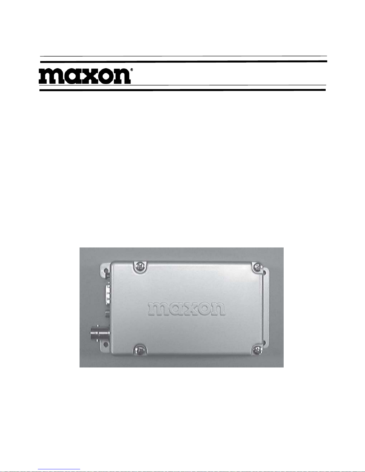
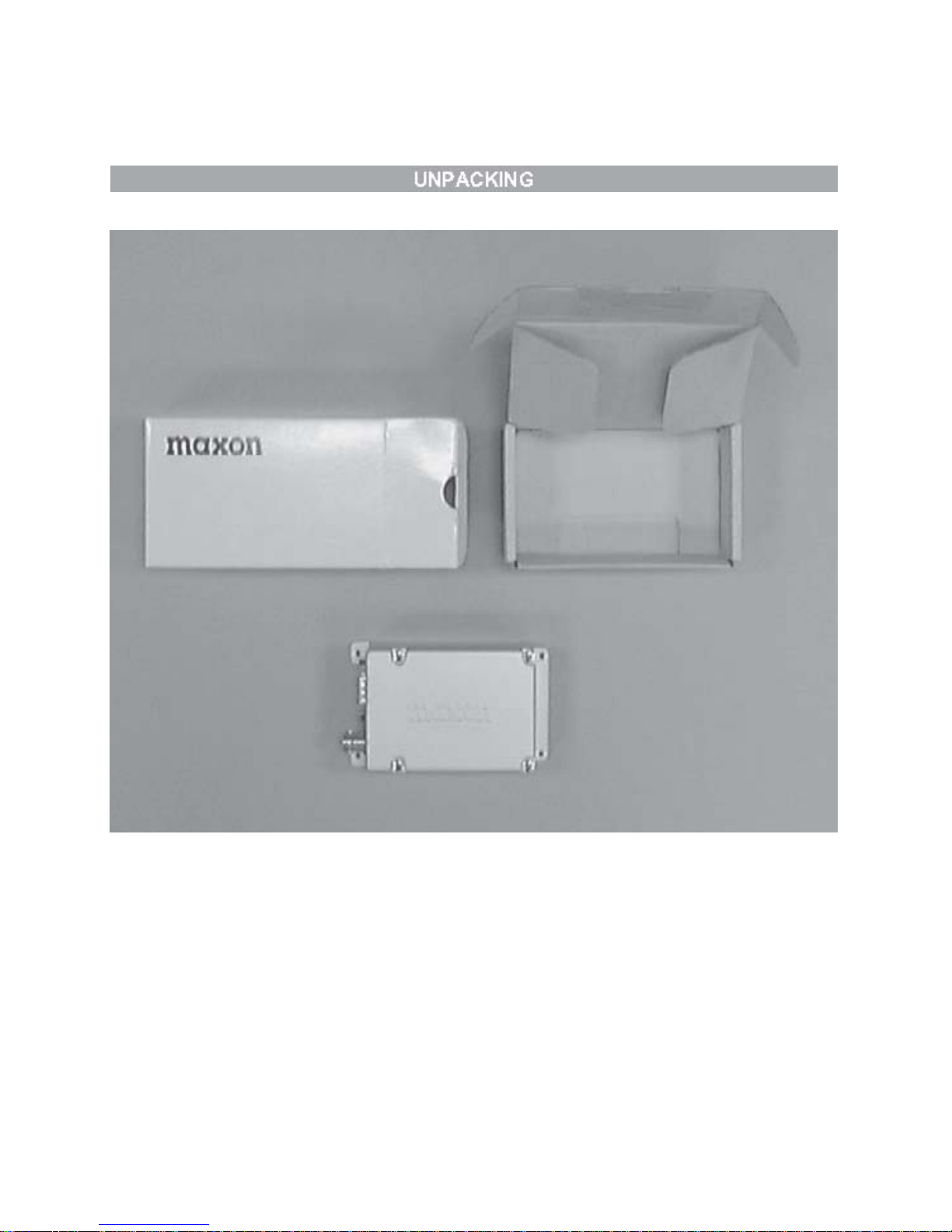
The SD-125 RF Link Module is the only item included in the shipping container.
Page 9

MAXONCIC
SD-125E RF LINK MODULE
- 9 -
FCC RF Exposure Compliance Requirements.
The Federal Communications Commission (FCC), with its action in General Docket 93-62, November 7,
1997, has adopted a safety standard for human exposure to Radio Frequency (RF) electromagnetic energy
emitted by FCC requlated equipment. Maxon subscribes to the same safety standard for the use of its
products. Proper operation of this radio will result in user exposure far below the Occupational Safety and
Health Act (OSHA) and Federal Communications Commission limits.
Power listed is conducted. This device must not exceed a maximum transmitting duty factor of 50%. The
antenna(s) used for this transmitter must be installed to provide a separation distance of at least 60cm
(20inches) from all persons. Must not be co-located or operating in conjunction with any other antenna or
transmitter, and must not exceed a gain of 6 dBi. Failure to observe these restrictions will result in
exceeding the FCC RF exposure limits.
About your SD-125E Series Data Radio
The MaxonCIC SD-125E Series of RF Link Modules from MaxonCIC utilizes the latest technology in its
design and manufacturing. Both the UHF and VHF models are PLL (Phase Lock Loop Synthesizer) /
microprocessor controlled, and offer one to five watts of power with 16 channel capability. Multiple
functions including 1200 to 2400 baud rates, AC and/or DC audio coupling, FFSK and FSK modulation are
standard in these fully programmable wide bandwidth RF Link Module units.
The radios are programmed using an IBM
®
Personal Computer, DOS® or WINDOWS® based software, an
interface module and a programming cable. This allows the radio to be tailored to meet the requirements of
the individual user and of the System(s) it is operating within.
Page 10

MAXONCIC
SD-125E RF LINK MODULE
- 10 -
Busy Channel Lockout
16 Channels
TX Time-out
Power Save
1 / 5 Watt Programmable Output
12.5 / 25 kHz Programmable Channel Spacing
Busy Channel Lockout
The Busy Channel Lockout feature, when enabled, disables the transmitter when the receiving channel is
busy and the user attempts to transmit.
16 Channels
The SD-125 Series radio can store up to 16 channels within the same band.
TX Time-out
The TX Time-out feature, when enabled, limits the amount of time that the user can continuously transmit.
This time can be set in increments of 10 seconds from 10 seconds to 990 seconds.
Power Save
The Power Save feature is used when an external battery is used as the power source. When Power Save is
enabled, the receiver “ON” and “OFF” time can be programmed into the radio and allows the operator to set
the length of time the receiver is asleep.
.
Page 11

MAXONCIC
SD-125E RF LINK MODULE
- 11 -
6.1 INTRODUCTION
The VHF and UHF radios are comprised of two PCB's (an RF PCB and a digital PCB). These boards are
connected with an 18 pin female and male connector . The digital board is interfaced with external data
equipment through the 9 pin d-sub male connector, which controls the radio and data receiving and sending .
6.2 DIGITAL CIRCUITS
The Digital circuit contains the CPU, the channel select switch, and associated digital circuits.
TX-SIGNAL CIRCUIT
The TX data signal comes from Pin 2 of Con 401, and goes through U404D. The TX-signal is amplified by
U406C. The TX-signal is filtered by U405A & B and U409A & B. which is a 4'th order low pass filter, the
output of U409A is then fed to the RF board for TX modulation.
RX-SIGNAL CIRC U IT
The RX-data signal comes from the RF board, which is connected with pin 10 of Con 403. The RX-signal is
switched by U404A and adjusted by RV403 and amplified by U407. The amplified signal goes to pin10 of
Con 401.
RSSI DETECTOR
From the RF board, the RSSI (Received Signal Strength Indicator ) signal flows to U403A & E through R461.
The pulse is injected from pin 5 of U403B every 1 mS and C451 is discharged. It is then charged by R464.
The RSSI signal is simultaneously input to pin 7 of U403A and those signals are compared. The compared
signal is output from U403A. Pin 1 of U403A and the CPU detects the pulse width. The pulse width is varied
by RSSI DC voltage, therefore, the carrier detection is controlled by the CPU.
EEPROM
RX / TX channel and RSSI detection level as well as other data from the programmer are stored in the
EEPROM. The data stored is retained without power supplied. This is a non-volatile memory. The EEPROM
may have information re-programmed or erased. U402 is an EEPROM with 2048 (8 x 256) capacity and data
is written and read serially.
CHANNEL SELECTOR
One of 16 channels may be selected using the Dip Switch (SW401). SW401 encodes the channel number,
selected into 4-bit binary code. The binary code plus one equals the channel number. The binary code is
decoded by the CPU enabling the appropriate RX or TX frequency and associated data to be selected from
the EEPROM.
DC TO DC CONVERTER
The main DC power is injected to the DC to DC converter . The DC to DC converter regulates the various
input power supply voltage and outputs a constant voltage of 7.5 Volts. It is a source for all of the RF and
digital circuits. The DC to DC converter is formed by IC801, Q801, Q802, L801 and R804. IC801 is a switch
mode DC to DC Converter IC. Input DC various appears as a voltage various through R804. IC801 detects
the voltage and controls the switching pulse. As the switching pulses, Q801and Q802 switches the input DC
of various supply voltages and generates the constant DC of supply voltage.
Page 12

MAXONCIC
SD-125E RF LINK MODULE
- 12 -
6.3 RF CIRCUITS
TRANSMITTER
The transmitter is comprised of:
1 Buffer
2 P.A. Module
3 Low Pass Filter
4 Antenna Switch
5 A.P.C. Circuits
BUFFER
VCO output level is -6dBm and amplified to +10dBm (UHF), +6dBm (VHF). The buffer consists of Q8 and
Q9 for isolation and gain.
P.A. BLOCK
The P.A Block uses a three stage amplifier and contains Q701, Q702, and Q703. Three stage amplifier Q701
amplifies the TX signal from +10 dBm to 100 mW. Q702 is amplified to 0.5W. Q503 amplifies to 6W and then
matched to 50 Ohms using the L.C. network, thereby reducing the harmonics by -30 dB.
LOW PASS FILTER
L7, L8, L9, C36, C37, C38 and C39 are the 7th order Chebyshev low pass filter. Unwanted harmonics are
reduced by -70 dBc.
ANTENNA SWITCH
When transmitting, the diodes D3 and D5 are forward biased enabling the RF signal passage to the antenna.
D5 is shorted to ground inhibiting the RF signal to front end. In receive the diodes D5 is reversed biased
passing the signal from the antenna through L10 and C61 to the front end without signal loss.
AUTOMATIC CURRENT CONTROL (ACC) CIRCUITS
The ACC circuit consists of R63, variable resistor RV4, IC5(B) and transistors Q11 and Q12. The supply
current is monitored by the difference voltage on R63 (0.1 Ohm). If the current varies by RF power output or
other reasons, it produces some bias voltage by IC5A and Q15. The differential signal at the output of IC5(B)
is passed to Q11 and Q12 that produces a constant power output to the antenna. RV4 is used to adjust the
RF power level.
Page 13

MAXONCIC
SD-125E RF LINK MODULE
- 13 -
6.4 RF CIRCUITS PLL SYNTHESIZER
12.8 MHz TCXO
The TCXO contains the 3-stage thermistor network compensation and crystal oscillator and modulation
ports. Compensation is ±5 PPM or less from -30c to +60c.
PLL IC DUAL MODULES PRESCALER
Input frequency of 12.8 MHz to Pin 1 of IC2 MB15E03SL is divided to 6.25 kHz or 5 kHz or 2.5KHz by the
reference counter, and then supplied to the comparator. RF signal input from VCO is divided to 1/64 at the
prescaler in IC2, divided by A and N counter in IC2 to determine frequency steps, and then supplied to the
comparator. PLL comparison frequency is 6.25/5/2.5kHz so that minimum programmable frequency step is
2.5/5/6.25 kHz. The A and N counter is programmed to obtain the desired frequency by serial data in the
CPU. In the comparator, the phase difference between reference and VCO signal is compared. When the
phase of the reference frequency is leading ,
ΦP is the output, but when VCO frequency is leading, ΦR is
the output. When
, ΦP= ΦR, phase detector out is a very small pulse.
EXTERNAL CHARGE PUMP
This is used to increase dynamic range of VCO. Voltage range is decided by the supply voltage of the
charge pump and the DC to DC converter which supplies that voltage. 0-12V is necessary for controlling the
VCO. In addition the radio adopts a current mode charge pump to take direct control of such parameters as
charge pump voltage swing, current magnitude, TRI-STATE leakage, and temperature compensation.
ΦP=
ΦR,
logic signals are converted into current pulses to enable either charging or discharging of the loop filter
components to control the output frequency of the PLL.
REFERENCE FREQUENCY LPF
The Loop Filter contains R9, C1 and C2. LPF settling time is 12mS with 1 kHz frequency. This also reduces
the residual side-band noise for the best signal-to-noise ratio.
DC TO DC CONVERTER
The DC to DC converter convert the 5v to 14-16v to supply the necessary voltage for wide range frequency
in the VCO.
VCO
The radio adopts a two VCO system for RX and TX in order to maximize each performance. The TX and RX
VCO generates RF carrier and local frequency and each VCO is switched by a TX/RX power source. It is
configured as a Colpitts oscillator and connected to the buffer as a cascade, the bias circuit is a cascade
configuration to save power. The varicap diode D201/D301 are low-resistance elements and have different
capacitance for reverse bias voltage. Using the change of reverse bias voltage (2~11V), the wanted
frequency for each channel can be obtained. L203/L303 are resonant coils and C208/C308 are used to
change the control voltage by the tuning core. D202 modulation diode modulates the audio signal. C204
compensates the non-linearity of the VCO due to the modulation diode and maintains a constant modulation
regardless of frequency.
Page 14

MAXONCIC
SD-125E RF LINK MODULE
- 14 -
6.5 RECEIVER
FRONT-END
The receive signal is routed backward through the low pass filter, then onward to C601 of the Hybrid
Receiver Front End Module to a bandpass filter consisting of (VHF C622 through C608, L607 through L604 )
and (UHF C601through C610, L601 through L603 ) is coupled to the base of Q601 which serves as an RF
amplifier. Diode D601 serves as protection from static RF overload from nearby transmitters. The output of
Q601 is then coupled to a second bandpass filter consisting of (VHF C607 through C623 and L604 through
L607).The output of C623 is then coupled to the doubly balanced mixer Q16. The receiver front end module
is factory pre-tuned and requires no adjustment. Repair is effected by replacement of the entire module of
the proper banded module. These are VHF 148MHz to 174 MHz and UHF 400 MHz to 490 MHz. The
receiver front end module signal pins are as follows:
1 RF Input
2 Input Ground
3 N/A
4 Receive +5V
5 Ground
6 Output
Page 15

MAXONCIC
SD-125E RF LINK MODULE
- 15 -
FIRST MIXER
Q16, L15 and C77 are Dual gate FET mixers which provide the 45.1 MHz intermediate frequency output.
The filtered frequency from the front end module is coupled to C131 The 45.1 MHz IF output is matched to
the input of the 2-pole monolithic filter by C65 and C66. The crystal filter provides a bandwidth of ±7.5 kHz
from the operating frequency providing a high degree of spurious and intermodulation protection. The IF
filter provides additional attenuation for the image frequency of the second mixer. The output impedance of
the filter is matched with the base of the post amplifier Q17 by C67 and C72
SECOND OSCILLATOR MIXER LIMITER AND FM DETECTOR
The output of the post filter amplifier, Q17, is coupled via C73 to the input of IC6(TA31136FN). IC6 is a
monolithic single conversion FM transceiver, containing a mixer, the second local oscillator, limiter and
quadrature detector. Crystal X1 44.645 MHz is used to provide resultant 455kHz signal from the output of
the
second mixer. The mixer output is then routed to CF1 (455F) or CF2 (455HT). These ceramic filters provide
the adjacent channel selectivity of 25 kHz or 12.5KHz bandwidth .
RSSI ( RECEIVER SIGNAL STRENGTH INDICATOR )
The RSSI signal is output from IC6 on pin 12. As the receiver signals the output, DC voltage is varied as
much as receiver signal strength. Also, the DC signal is temperature compensated with a thermistor (TH1).
would cause the CD (Carrier Detect) to act intermittently.
Page 16
MAXONCIC
SD-125E RF LINK MODULE
- 16 -
7.1 GENERAL
When removing or fitting, use the Exploded View and Parts List, located on page 28 in conjunction with the
following procedures:
• WARNING: Disconnect the SD-125E from all external equipment at the D-Sub connector prior to
disassembly.
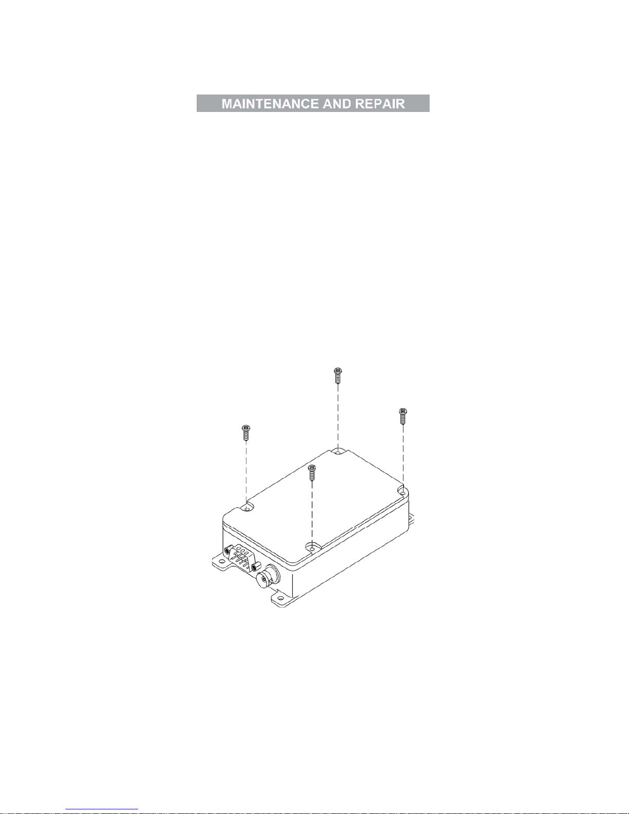
7.2 REMOVING & REPLACING THE UPPER COVER
Removing the Upper Cover:
1. Unscrew the four upper cover mounting screws located on the upper cover of the radio.
To replace the Upper Cover:
1. Reverse the steps taken to remove the Upper Cover.
Figure 1-Upper Cover Removal
Page 17
MAXONCIC
SD-125E RF LINK MODULE
- 17 -
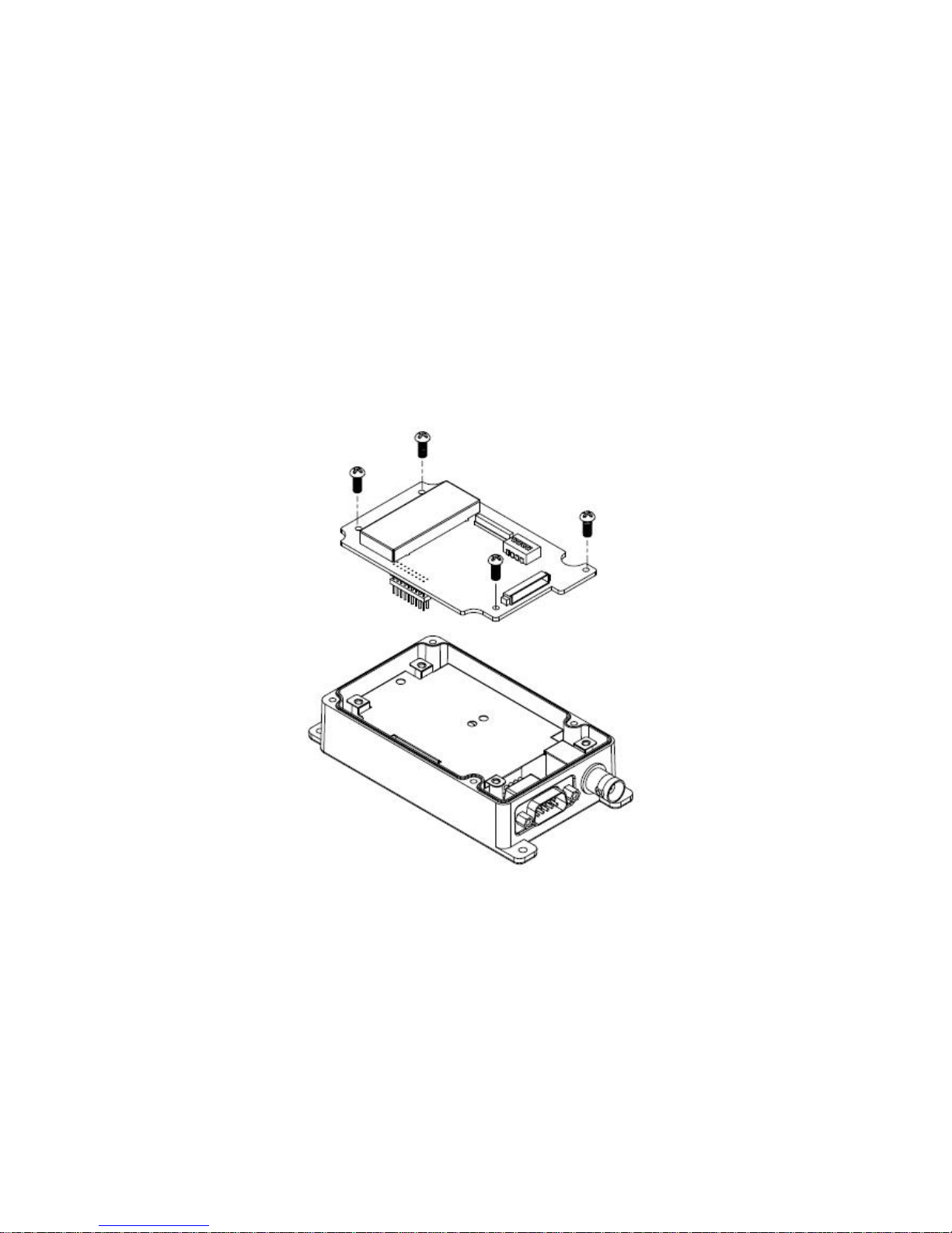
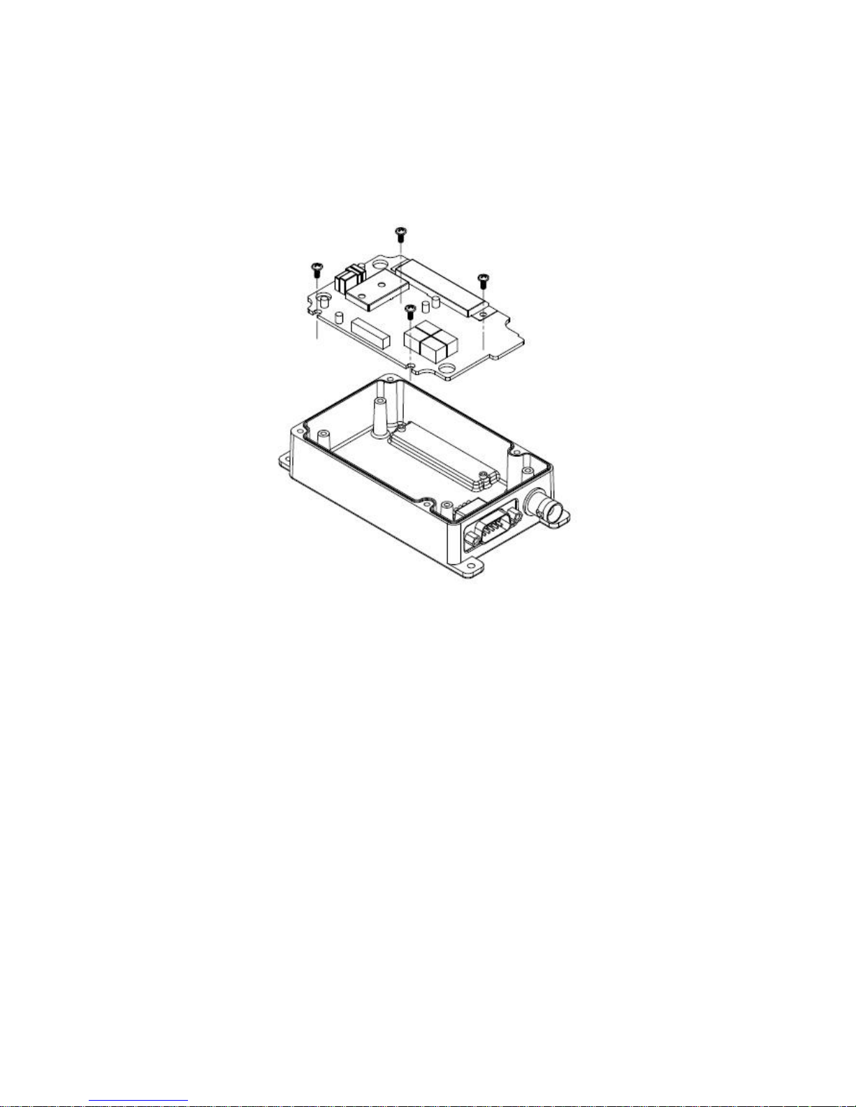
7.3 REMOVING & REPLACING THE DIGITAL BOARD & SHIELD PLATE
Removing the Digital Board Assembly & Shield Plate:
1 Remove the Upper Cover (refer to Removing & Replacing the Upper Cover).
2 Disconnect the DB9 pin connector on CON401.
3 Unscrew the 4 mounting screws.
4 Remove the Digital Board Assembly.
5 Remove the Shield Plate.
To replace the Digital Board Assembly:
1. Reverse the steps taken to remove the Digital Board Assembly & Shield Plate.
Figure 2-Digital Board Assembly Removal
Page 18

MAXONCIC
SD-125E RF LINK MODULE
- 18 -
Figure 3-Shield Plate Removal
7.4 REMOVING & REPLACING THE RF BO ARD
Removing the RF Board Assembly:
1 Remove the Upper Cover (refer to Removing & Replacing the Upper Cover).
2 Remove the Digital Board Assembly and Shield Plate
(refer to Removing & Replacing the Digital Board Assembly & Shield Plate).
3 Unscrew the 4 mounting standoffs.
4 Unsolder the antenna connector cable.
5 Remove the RF Board Assembly.
To replace the RF Board Assembly:
Page 19
MAXONCIC
SD-125E RF LINK MODULE
- 19 -
1. Reverse the steps taken to remove the RF Board Assembly.
Figure 4-Rf Board removal
Page 20

MAXONCIC
SD-125E RF LINK MODULE
- 20 -
The SD-125E Series radio requires the ACC-900E Programming Software, ACC-2125 Interface Cable, 9-15
VDC 200mA Power Supply. Refer to the ACC-900E Programming User’s Manual for detailed information on
programming the SD-125E Series radio.
The SD-125E UHF/VHF Receiver is by design, broad band covering UHF(400-430 MHz & 440-470 MHz
&470-490 MHz) and VHF(148-174 MHz) and should require no special alignment, unless repairs are
performed on the receiver portion.
Should repairs be necessary, use the "Test Equipment Diagram" on page 23& the "Alignment Points
Diagram" on page 24, in conjunction with the following procedures:
• After just opening the upper cover, Power High/Low, Modulation level, Modulation balance and
Frequency can be directly controlled through holes at the digital PCB’ s.
9.1 RECEIVER
1 Apply a standard test signal to the receiver antenna terminals.
2 Adjust RV403 for the specific audio output level.
RX VCO
1 Set the unit to the highest receive frequency 430MHz(UHF1), 470MHz(UHF2), 490MHz(UFH3),
174MHz(VHF) and verify the VCO control voltage is under 9.0 Volts. If it’s over 9.0 Volts, adjust C308 of RX
VCO to 9.0 Volts
2 Set the unit to the lowest receive frequency 400MHz(UHF2), 440MHz(UHF2), 470MHz(UFH3),
148MHz(VHF) and verify that the VCO voltage is above 2.0 Volts. Adjust C308 to 2.0Volts.
• Note: Use TP1 to measure the voltage.
9.2 TRANSMITTER
Connect the unit to a Service Monitor with the power meter setting to the 10 W scale (or autorange)
TCXO
Set the channel selector to the mid-range frequency 460 MHz, adjust RV1 for a reading of 460 MHz ±200Hz
(155 MHz VHF models).
Page 21

MAXONCIC
SD-125E RF LINK MODULE
- 21 -
TX VCO
1. Set the unit to the highest receive frequency 430MHz(UHF1), 470MHz(UHF2), 490MHz(UFH3),
174MHz(VHF) and verify the VCO control voltage is under 9.0 Volts. If it’s over 9.0 Volts, adjust C308 of RX
VCO to 9.0 Volts
2. Set the unit to the lowest receive frequency 400MHz(UHF2), 440MHz(UHF2), 470MHz(UFH3),
148MHz(VHF) and verify that the VCO voltage is above 2.0 Volts. Adjust C308 to 2.0Volts.
• Note: use TP1 to measure the voltage.
TX Deviation and Balance Adjustment
1 Set the unit to a mid-frequency and input the TX data with 400 Hz standard audio level.
2 Increase the signal level to 20 dB from standard level.
3 Monitor the demodulated signal from service monitor. Adjust RV7 to make the monitored signal to be
a balanced square wave.
4 Reduce input signal to the standard level and adjust RV2 for the standard deviation.
APC
1 Adjust RV4 for High Power (5W)
2 Adjust RV3 for Low Power (1W)
3 This completes the transmitter alignment procedures.
Page 22

MAXONCIC
SD-125E RF LINK MODULE
- 22 -
SD-125 Squelch setting using the ACC-900E PC Program and TAJ-521D Interface Cable.
Maxon’s wide range of data radio products since the crystal control module (DM-0500 series) had their
squelch level setting by hardware touch up. With the SD-125E series, the squelch level to open or close
(unmute or mute) is set up by software control.
The RSSI utilizes the A/D conversion that will be fed to the microprocessor, which in turn will use this input
to determine the squelch level setting to control the mute and unmute of the receiver.
Default setting of squelch level for all the SD-125 from our manufacture and workshop is approximately set
at:
1. Squelch open (unmute) at -114dBm to -113dBm (0.45 -0.5mV of the RX signal strength)
2. Squelch close (mute) at -117dBm to -116dBm (0.3 - 0.35mV of the RX signal strength)
Changing the default squelch settings requires use of the programming cable and software Those are
designed for use not only as part of the programming kit but also as a tool of squelch level setting.
The minimum equipment required for squelch level setting is a RF signal generator. Radio communication
test equipment is recommended.
1 Connect DB-9 with power cable to the Radio and DB-9 without power cable to the PC
2 Its antenna connector to the RF input port of the RF signal generator.
3 Execute ACC-900E and then select Squelch to the tool bar.
4 Power up the ACC-900E by plugging power plug to the power supply.
(use the DC supply of9-15 Volts 200mA).
5 Select “ user” menu of squelch program menu of ACC-900E
6 Reset the power supply and press the next button.
7 Adjust the RF signal generator for the desired signal strength to unmute level and press the next
button (e.g. default setting is -113dBm, that is equivalent to 0.5mV)
8 Configure mute level and press the next button.
9 Press the next button to confirm
z It is recommended you should step other jobs while configuration.
• NOTE: The difference of RF signal strength between the unmute and mute levels must be greater
than or at least equal to 0.15mV (i.e. at least -123.5dBm) for the squelch setting to work properly. If they
are too close to one another, RSSI through the A/D conversion can not differentiate between the mute and
unmute level properly. As a result, it would cause the CD (Carrier Detect) to act intermittently.
Page 23

MAXONCIC
SD-125E RF LINK MODULE
- 23 -
Page 24

MAXONCIC
SD-125E RF LINK MODULE
- 24 -
RF BOARD DIGITAL BOARD
ALIGNMENT POINTS ALIGNMENT POINTS
SW401
CHANNEL SELECT SWITCH
Page 25

MAXONCIC
SD-125E RF LINK MODULE
- 25 -
Surface Mount Co m p on e n ts
Surface mount components should always be replaced using a temperature controlled soldering system. The
soldering tools may be either a temperature controlled soldering iron or a temperature controlled hot-air
soldering station. A hot-air system is recommended for the removal of components on these boards. With
either soldering system, a temperature of 700° F (371° C) should be maintained.
The following procedures outline the removal and replacement of surface mount components. If a hot-air
soldering system is employed, see the manufacturer’s operating instructions for detailed information on the
use of your system.
CAUTION: Avoid applying heat to the body of any surface mount component using standard soldering
methods. Heat should be applied only to the metalized terminals of the components. Hot-air systems do not
damage the components since the heat is quickly and evenly distributed to the external surface of the
component.
CAUTION: The CMOS Integrated Circuit devices used in this equipment can be destroyed by static
discharges. Before handling one of these devices, service technicians should discharge themselves by
touching the case of a bench test instrument that has a 3-prong power cord connected to an outlet with a
known good earth ground. When soldering or desoldering a CMOS device, the soldering equipment should
have a known good earth ground.
Surface Mount Removal
1 Grip the component with tweezers or small needle nose pliers.
2 Alternately heat the metalized terminal ends of the surface mount component with the soldering iron.
If a hot-air system is used, direct the heat to the terminals of the component. Use extreme care with the
soldering equipment to prevent damage to the printed circuit board (PCB) and the surrounding components.
3 When the solder on all terminals is liquefied, gently remove the component. Excessive force may
cause the PCB pads to separate from the board if all solder is not completely liquefied.
It may be necessary to remove excess solder using a vacuum de-soldering tool or Solder wick . Again,
use great care when de-soldering or soldering on the printed circuit boards. It may also be necessary
to remove the epoxy adhesive that was under the surface mount component and any flux on the
printed circuit board.
Page 26

MAXONCIC
SD-125E RF LINK MODULE
- 26 -
Surface Mount Component Replacement
1 “Tin” one terminal end of the new component and the corresponding pad of the PCB. Use as little
solder as possible.
2 Place the component on the PCB pads, observing proper polarity for capacitors, diodes, transistors,
etc.
3 Simultaneously touch the “tinned” terminal end and the “tinned” pad with the soldering iron. Slightly
press the component down on the board as the solder liquefies. Solder all terminals, allowing the component
time to cool between each application of heat. Do not apply heat for an excessive length of time and do not
use excessive solder.
With a hot-air system, apply hot air until all “tinned” areas are melted and the component is seated in place.
It may be necessary to slightly press the component down on the board. Touch up the soldered connections
with a standard soldering iron if needed. Do not use excessive solder.
• CAUTION: Some chemicals may damage the internal and external plastic parts of the radio.
4. Allow the component and the board to cool and then remove all flux from the area using alcohol or
another approved flux remover.
Surface Mounted Integrated Circuit Replacement
Soldering and de-soldering techniques of the surface mounted IC’s are similar to the above outlined
procedures for the surface mounted chip components. Use extreme care and observe static precautions
when removing or replacing the defective (or suspect) IC’s. This will prevent any damage to the printed
circuit board or the surrounding circuitry. The hot-air soldering system is the best method of replacing
surface mount IC’s. The IC’s can easily be removed and installed using the hot-air system. See the
manufacturer’s instructions for complete details on tip selection and other operating instructions unique to
your system. If a hot-air system is not available, the service technician may wish to clip the pins near the
body of the defective IC and remove it. The pins can then be removed from the PCB with a standard
soldering iron and tweezers, and the new IC installed following the Surface Mount Component Replacement
procedures. it may not be necessary to “tin” all (or any) of the IC pins before the installation process.
Page 27

MAXONCIC
SD-125E RF LINK MODULE
- 27 -
SYMPTOMS CAUSES COUNTERMEASURES
Unit does not work
1. Incomplete connection
2. Defective DC/DC VCC
3. 5v voltage source
4. PLL error
5. EEPROM fail
1. Check CON401 connection
2. Check IC801
3. IC1 (5v ±0.2v)
4. Check VTCXO/VCO/PLL IC
5. Re-programming
Bad RX Sensitivity
(-10 to -80dBm)
1. Defective ANT Switch
2. Defective Front-End
3. Defective Dual Gate FET
4. IF IC
5. VCO level drop
6. Change of 1
st local frequency
1. Check D3, D5
2. Check Q601
3. Check Q16
4. Replace IC6
5. RX VCO level > -2dBm
6. Check 12.8MHz
Defective RX
1. VCO frequency change or
level drop
2. Defective voltage source
1. Repair RX VCO
Defective IF IC (IC6)
3. IC1, Q2
PLL Error
1. Defective 12.8 MHz VTCXO
2. Voltage source for RX VCO/
TX VCO
3. Defective PLL IC
1. Replace VTCXO
2. Check RX VCO/TX VCO
3. Replace IC2
Low TX Power Output
1. APC 1. Re-adjust RV4
No TX Power
1. TX Buffer
2. Power Module
3. APC control
1. Check Q9, 10
2. Check Q701, 702, 703
3. Check Q11
No Modulation
1. SW IC & Mic Amp IC 1. Check U404, 405, 406
No Programming
1. Short protector VCC 1. Defective programming lead
Page 28

MAXONCIC
SD-125E RF LINK MODULE
- 28 -
Pin1..... Audio In (Data RX)
Pin2..... Audio Out (Data TX)
Pin3.....PTT
Pin4.....GND (Ground)
Pin5.....B+ (8-18 Volts DC)
Pin6..... Carrier Detect (Squelch)
Pin7.....N/C No Connect
Pin8..... Switch
SD125E RF BOARD P.C.B. SD125E DIGITAL BOARD P.C.B
(P/N : 932-558193AB)
D-SUB 9 CONNECTOR
(P/N : 501-394001BA)
Page 29

MAXONCIC
SD-125E RF LINK MODULE
- 29 -
COMPONENT PINOUT
BASE DIAGRAM
MANUFACTURER’S
PART NUMBER
REFERENCE NO. SYMBOL
AT-41532 Q601
KTC4075 Q3.4.901.902.903.904
2SC5086-Y Q201.202.301.302
KTA2014 Q5.6.905
PBR951 Q10.701
BFR92A Q7.17.19
KTC3875S Q8.12.15.20
KTA1504S Q407
KRC104S (ND)
Q13.14.18.21.22.24
404.406.408
KRA104S (PD) Q7.23.401.402.403.405
KRA110S (PK) Q1.Q2
KDS181 D1.8.9.701
KDS193 D2.406
KDS226 D601.901.902
ZENER (5.6V)
D401.402.403.404
405.407.408.409.410
Page 30

MAXONCIC
SD-125E RF LINK MODULE
- 30 -
1SV229
1SV217
D201.202.301
KDS160 D801
UPP9401 D3.D5
KIA7042AF U408
SI4412DY Q801.802
BLT50 Q702
3SK324UG Q16
UPD78F0513 U401 MCU
MB15E03SL IC2 PLL IC
TA31136FN IC6 IF IC
NJM12903V Comparator
NJM12904V IC3.4.5 OP AMP
Page 31

MAXONCIC
SD-125E RF LINK MODULE
- 31 -
LTC1435CS IC801
MC14066BD U404 Analog S/W IC
KIA324F U405.406.409
OP AMP
COMPANDER
LM339 U403
Quad Voltage
COMPARATOR
AT93C56-10SI U402 EEPROM
LM386MX U407 AUDIO AMP
TK71750SCL
TK71733SCL
IC7
IC1
VOLTAGE
REGULATOR IC
2SK3476
1(Gate)
2(Source)
3(Drain)
Q703
Silicon N-Channel
MOS TYPE
Amplifier
KTA1663 Q11
PNP Epitaxial
PlanarTransistor
Page 32

Page 33

Page 34

Page 35

Page 36

Page 37

Page 38

Page 39

Page 40

Page 41

Page 42

Page 43

Page 44

Page 45

Page 46

Page 47

MAXONCIC
SD-125E RF LINK MODULE
SD-125E COMMON PARTS LIST
COVER ASSY (501-502121CB)
Reference No Description Code No Reference No Description Code No
M2.6X6 NI-PLAT 838-602606NI SPTE 0.3T 832-501337AA
M3X10 (+)BH ZN-PLAT WHT 838-600310ZN CHANNEL SELECTION LABEL 835-130084AA
PH(+), M2X4 WD=4.7 NI-PLAT 838-320204NI POLYESTER 48X8 835-130036AA
NSP T0.2 832-501175AA POLYESTER 40X21 835-130048AA
SD-125, ALDC12 832-501268AA POLYESTER 39.5X20.5 835-130040AA
NEOPRENE 3M4262 833-501060AA SHD-60503 922-620001AB
0.4&1.2&X260 SILI.RUBB BLK 833-501064AA UG-1094/U(W) 925-990002ZA
SD-125E, ALDC12 832-501032BB 15P+9P SHD-7B03 501-394001BA
PACKING ASSY(501-902121PA)
Reference No Description Code No Reference No Description Code No
SKE 136(W)X72(D)X42(H) 836-120072AA ART PAPER 60X25 835-130083AA
MANILA 73.5(W)X140(D)X42.5(H) 836-120073BB ART PAPER STICKER 835-130226AA
P.E 100X150XT0.05 836-140011AA DW1E 281(W)X372(D)X187(H) 836-120071AA
CH SPACING ASSY(501-502121SA)
Reference No Description Code No Reference No Description Code No
Y1 CDBCB455KCAY24-R0 928-290455KC X1 44.645MHZ -30 15PPM 32PF 928-130001AL
XF1.2 45.1MHz, 45N15B4 929-300045NC CF2 LTWM455HT(2.832.689) 929-310455HTAC
SILICONE RUBBER HS50 GRAY 833-501042AA CF1 LTM455FW(2.832.685) 929-310455FWAC
SD-125E U1 PARTS LIST
SD-125E U1(400MHz~430MHz) DIGITAL BOARD(932-558193AA) PARTS LIST
DC TO DC CONVERSION ASSY (501-902128AA)
Reference No Description Code No Reference No Description Code No
R801 10K 1/16W 5% 1608 911-610057BG C810 0.01UF GRM39X7R103K25V 913-421004EK
R802 36K 1/16W 5% 1608 911-636057BG C802.808 0.1UF G RM39 X7R104K50V 913-421005HH
R804 0.033 1/10W 1% 2012 911-603307CA C805.806.812 100PF GRM39 U2J101J 50V 913-421002HGAB
R805 68K 1/16W 5% T 1608 911-668057BG C803 330PF GRM39COG331J50V 913-423302HG
R806 20K 1/16W 5% T 1608 911-620057BG C801.804 51PF GRM39COG510J50V 913-425101HG
C811.815 100UF 16V D 20% 915-611008ZC D801 KDS160 882-190160AA
C807 22UF 35V D 20% 915-612207FKLG D802 MBRS140T3 882-690140TA
C813 4.7UF 10V A 20% 915-6114706 L801 12UH DA104-120M 9 19-922120AB
Q801.802 SI4412DY 881-694412DY L802 3.3UH SD73-3R3M 919-921330AB
IC801 LTC1435CS(SO-16) 875-401435SP NSP T0.3 832-501180AA
DIGITAL PCB MANUAL ASSY (501-402128AA)
Reference No Description Code No Reference No Description Code No
CON403 2.0MM DUAL ROW DOUBLE (2X9) 925-990016AA SW401 KSD-04 924-150004AA
CON404 TDI7-14SG 925-990100AA CON06 TDH2-08SG 925-990101AA
CON401.402 53261-1571 925-990015AB
Page 48

MAXONCIC
SD-125E RF LINK MODULE
SD-125E U1(400MHz~430MHz) DIGITAL BOARD(932-558193AA) PARTS LIST
DIGITAL PCB SMD ASSY (501-402128AB)
Reference No Description Code No Reference No Description Code No
R134.135.471 0 1/16W 5% 1608 911-600007BG C411 0.0015UF CM105X7R152K50V 913-421503HHAA
R472.473.485 0 1/16W 5% 1608 911-600007BG C406.420.451 0.01UF GRM39X7R103K25V 913-421004EK
LK6.7.8.10.12 0 1/16W 5% 1608 911-600007BG C68.404.407.416 0.1UF GRM39Y5V104Z25V 913-421005EX
LK14.15.18 0 1/16W 5% 1608 911-600007BG C417.422.436.450 0.1UF GRM39Y5V104Z25V 913-421005EX
R490 10 1/16W 5% T 1608 911-610027BG C463.464 0.1UF GRM39Y5V104Z25V 913-421005EX
R49.137.446.474 100 1/16W 5% T 1608 911-610037BG C402.421.429.430 0.001UF GRM39 X7R102K 50V 913-421003HH
R475.476.477.501 100 1/16W 5% T 1608 911-610037BG C431.433.434.448 0.001UF GRM39 X7R102K 50V 913-421003HH
R423.481.482.483 1K 1/16W 5% 1608 911-610047BG C452.442.443.444 0.001UF GRM39 X7R102K 50V 913-421003HH
R484 1K 1/16W 5% 1608 911-610047BG C445.446.432 0.001UF GRM39 X7R102K 50V 913-421003HH
R403.419.421.424 10K 1/16W 5% 1608 911-610057BG C410 0.0022UF GRM39X7R222J50V 913-422203HG
R425.435.437.440 10K 1/16W 5% 1608 911-610057BG C419.466 0.0027UF GRM39X7R272J50V 913-422703HG
R505.465.468.489 10K 1/16W 5% 1608 911-610057BG C403 0.022UF GRM39X7R223K50V 913-422204HH
R407.415.131.132 10K 1/16W 5% 1608 911-610057BG C412 0.0039UF GRM39X7R392K50V 913-423903HH
R133.416.417.418 10K 1/16W 5% 1608 911-610057BG C413.465 0.0033UF GRM39X7R332K50V 913-423303HHAA
R447.454.497.461 10K 1/16W 5% 1608 911-610057BG C418 0.0047UF GRM39X7R472K50V 913-424703HH
R426.428.460.478 10K 1/16W 5% 1608 911-610057BG C409.423.426 0.047UF GRM39Y5V473Z25V 913-424704EX
R487.488.422.400 10K 1/16W 5% 1608 911-610057BG C414 0.0068UF GRM39X7R682K50V 913-426803HH
R498.499.502.503 10K 1/16W 5% 1608 911-610057BG C400.401.439 1UF GRM40Y5V105Z16V 913-431006CX
R409.411.414.445 100K 1/16W 5% 1608 911-610067BG C405.408.458 120PF GRM39COG121J50V 913-421202HG
R451.452.458.480 100K 1/16W 5% 1608 911-610067BG C126.129.130.459 220PF GRM39COG221J 50V 913-422202HG
R492.493.494.495 100K 1/16W 5% 1608 911-610067BG R469 220PF GRM39COG221J 50V 913-422202HG
R448.430 1M 1/16W 5% 1608 911-610077BG C437.438 39PF GRM39COG390J50V 913-423901HG
R456 150 1/16W 5% T 1608 911-615037BGAA C415 47PF GRM39COG470J50V 913-424701HG
R449 20K 1/16W 5% T 1608 911-620057BG C424 470PF GRM39X7R471K 50V 913-424702HH
R413 200K 1/16W 5% 1608 911-620067BG C427 100UF 6.3V D 20% 915-611008ZA
R438 2.2K 1/16W 5% T 1608 911-622047BG C425.440.460 10UF 6.3V A 20% 915-611007AKLC
R406.455.457 22K 1/16W 5% T 1608 911-622057BG C461 1UF 25V A 20% 915-611006EKLC
R412 2.7K 1/16W 5% T 1608 911-627047BG C447 33UF 25V D 20 % 915-613307EKLG
R410 270K 1/16W 5% 1608 911-627067BG C435.454.456.457 4.7UF 10V A 20% 915-6114706
R450 33K 1/16W 5% 1608 911-633057BG C428 47UF 16V D 20% 915-614707
R420 3.9K 1/16W 5% 1608 911-639047BG
R433.434.436.439 4.7K 1/16W 5% 1608 911-647047BG U401 UPD 78F0513 874-180513LQ
R404,431,432,441 47K 1/16W 5% 1608 911-647057BG U405.406.409 KIA324F-EL 875-100324FL
R442,443,444,464 47K 1/16W 5% 1608 911-647057BG U408 KIA7042AF 875-907042SO
R466,467.429 47K 1/16W 5% 1608 911-647057BG U403 LM339 875-900339AA
R453 5.6K 1/16W 5% 1608 911-656047BG U404 MC14066BDR2G 874-114066BD
R491.494 56K 1/16W 5% 1608 911-656057BG U402 AT93C56-10SI 876-609356AA
R473.486 68K 1/16W 5% T 1608 911-668057BG U407 LM386MX-1 (SO-08) 875-100386SP
R136 9.1K 1/16W 5% 1608 911-691047BG U401.402.403.404 BZX84C5V6LT1 882-290084CB
RV404 0 1/10W 5% 2012 911-600007CA U405.407.408.409 BZX84C5V6LT1 882-290084CB
R463 1.8M 1/10W 5% 2012 911-618077CA U410 BZX84C5V6LT1 882-290084CB
Q404.406.408 KRC104SND(SOT-23) 881-390104SN X401 ZTTCC3.58MG 928-210358MG
Q407 KTA1504SY(SOT-23) 881-191504SY
Q401.402.403.405 KRA104S(SOT-23) 881-190104SPAA D406 KDS193 882-190193KD
SD-125E U1(400MHz~430MHz) RF BOARD(932-558195AB) PARTS LIST
PWR MODULE U1 ASSY (501-902128AE)
Reference No Description Code No Reference No Description Code No
R705 10K 1/16W 5% 1608 911-610057BG C711 0.001UF GRM40 X7R102K 50V 913-431003HH
R706 100 1/16W 5% T 1005 911-610037BF C709 0.01UF GRM36X7R103K16V 913-411004CH
R707 220 1/16W 5% 1005 911-622037BF C702 10PF GRM36COG100D50V 913-411001HC
R704 2.2K 1/16W 5% T 1005 911-622047BF C705 15PF GRM40COG150J50V 913-431501HG
R701 2.7K 1/16W 5% 1005 911-627047BF C713 20PF GRM40COG200J50V 913-432001HG
R709 330 1/16W 5% 1005 911-633037BF C712 220pF, GRM40COG221J50V 913-432202HG
R702 6.8K 1/16W 5% 1005 911-668047BF C708 43PF GRM40COG430J50V 913-434301HG
R703 6.8 1/16W 5% 1005 911-668017BF C716 27PF GRM40COG270J50V 913-432701HG
Q701 PBR951 881-990951AA C704 3PF GRM36COG030C50V 913-413000HB
D701 KDS181S 882-190181SA C714.722 6PF GRM40COG060D50V 913-436000HC
L705 1.0X0.45X4T:R(SMD) 919-490024AA C707 7PF GRM40COG070D50V 913-437000HC
L701.703 14NH 03095TL 919-420046AA C701 22PF GRM36COG220J50V 913-412201HGAA
L702 1.2UH SWI0805FT1R2 919-920120AB Q702 BLT50(SOT-223) 881-990050AA
L704 3.9NH SWI0603CT3N9 919-920003AA Q703 2SK3476 (TE12L,Q) 881-883476AA
C721 9PF GRM40COG090D50V 913-439000HC
NSP T0.2 832-501170AA C700.703.706 220PF GRM36X7R221J50V 913-412202HGAA
Page 49

MAXONCIC
SD-125E RF LINK MODULE
SD-125E U1(400MHz~430MHz) RF BOARD(932-558195AB) PARTS LIST
FRONT END U1 BAND ASSY (501-372128AA)
Reference No Description Code No Reference No Description Code No
R(C607.C603) 0 1/16W 5% 1005 911-600007BF C609.617 12PF GRM36COG120J50V 913-411201HG
R(C604,C605) 0 1/16W 5% 1005 911-600007BF C619 15PF GRM36 COG150J 50V 913-411501HG
R602 47 1/16W 5% T 1005 911-647027BF C620 18PF GRM36COG180J50V 913-411801HG
R601 47K 1/16W 5% T 1005 911-647057BF C616.623 20PF GRM36COG200J50V 913-412001HGAA
C615 3.3PF GRM36COG3R3C50V 913-413300HB
Q601 AT-41532 881-394153AA C614.621 4PF GRM36COG040C50V 913-414000HBAA
D601 KDS226 882-190226AA C601.613 4.7PF GRM36COG4R7 913-414700
L607.608 14NH 03095TL 919-420046AA C611 470PF GRM36X7R471K50V 913-414702HH
L601.602.605 0.30X0.90X4T:R(SMD) 919-420052AA C618 5.6PF GRM36COG5R6D50V 913-415600HC
L606.609 0.30X0.90X4T:R(SMD) 919-420052AA C622 8PF GRM36COG080D50V 913-418000HC
VOLTAGE DOUBLER ASSY (501-392128AA)
R908 10 1/16W 5% 1005 911-610027BF C911 0.1UF GRM36Y5V10 4Z16V 913-411005CK
R905.907 2.2K 1/16W 5% T 1005 911-622047BF C904.905.908.909 0.022UF GRM36X5R223K16V 913-412204CH
R901.903 27K 1/16W 5% 1005 911-627057BF C910 0.022UF GRM36X5R223K16V 913-412204CH
R906 4.7K 1/16W 5% T 1005 911-647047BF C901.902 220PF GRM36X7R221J50V 913-412202HGAA
R902.904 7.5K 1/16W 5% 1005 911-675047BF Q901.902.903.904 KTC4075-Y 881-394075YA
Q905 KTA2014-Y 881-192014YA
D903 0 1/10W 5% 2012 911-600007CA D901.902 KDS226 882-190226AA
RF CIRCUIT ASSY (501-382128AA)
R3.4 910 1/16W 5% 1608 911-691037BG C73.78.84.114 0.001U F GRM36X7R102K50V 913-411003HH
R59.61 100K 1/16W 1% T 1608 911-610065BG C121,131 0.001UF GRM36X7R102K50V 913-411003HH
R60.126 68K 1/16W 1% 1608 911-668055BG C11.45.69.83.86.95 0.01UF GRM36X7R103K16V 913-411004CH
R(C62).R79.LK17 0 1/16W 5% 1005 911-600007BF C105.107.117.123 0.01UF GRM36X7R103K16V 913-411004CH
R14.53 10 1/16W 5% 1005 911-610027BF C124 0.01UF GRM36X7R103K16V 913-411004CH
R1.2.12.38.49.72 100 1/16W 5% T 1005 911-610037BF C7.10.85.87.97.103 0.1UF GRM36Y5V104Z16V 913-411005CK
R88.127 100 1/16W 5% T 1005 911-610037BF C110.111 0.1UF GRM36Y5V104Z16V 913-411005CK
R37.47.77.87 1K 1/16W 5% T 1005 911-610047BF C46.74.76.79.115 0.1UF GRM36X5R104K10V 913-411005BH
R7.8.16.20.22.25 10K 1/16W 5% T 1005 911-610057BF C116.118 0.1UF GRM36X5R104K10V 913-411005BH
R26.46.67.81.82.99 10K 1/16W 5% T 1005 911-610057BF C120 0.22UF GRM39X7R224K10V 913-422205BH
R105.109.107.110 10K 1/16W 5% T 1005 911-610057BF C54 0.47UF GRM40Y5V474Z16V 913-434705CX
R111.121.124 10K 1/16W 5% T 1005 911-610057BF C96.102 0.0047UF GRM36X7R472K25V 913-414703EH
R93 100K 1/16W 5% T 1005 911-610067BF C22.62.99 1UF GRM40Y5V105Z16V 913-431006CX
R51.106 1M 1/16W 5% T 1005 911-610077BF C61 10PF GRM40COG10 0C50V 913-431001HB
R39 120 1/16W 5% 1005 911-612037BF C66 11PF GRM39COG110J50V 913-421101HG
R28.97 1.2K 1/16W 5% T 1005 911-612047BF C80 15PF GRM36 COG150J 50V 913-411501HG
R52.35.66 12K 1/16W 5% 1005 911-612057BF C24 2.4pF, GRM36COG2R4C 50V 913-412400HB
R48 1.5K 1/16W 5% T 1005 911-615047BF C71 220PF GRM36X7R221J50V 913-412202HGAA
R100 15K 1/16W 5% T 1005 911-615057BF C5.9.13.18.23.49 220PF GRM36COH221J25V 911-412201EG
R80 150K 1/16W 5% 1005 911-615067BF C98.101.108.109 220PF GRM36COH221J25V 911-412201EG
R13.33 18 1/16W 5% 1005 911-618027BF C113 220PF GRM36COH221J25V 911-412201EG
R75 1.8K 1/16W 5% 1005 911-618047BF C81 27PF GRM36COG270J50V 913-412701HG
R24 18K 1/16W 5% T 1005 911-618057BF C21 3PF GRM36COG030C50V 913-413000HB
R92 180K 1/16W 5% 1005 911-618067BF C72 30PF GRM36COG300J50V 913-413001HG
R19.102.103.108 20K 1/16W 5% T 1005 911-620057BF C82 33PF GRM36COG330J50V 913-413301HG
R17 22 1/16W 5% T 1005 911-622027BF C33 3.9PF GRM36COG3R9C50V 913-413900HB
R27.31.56 220 1/16W 5% 1005 911-622037BF C34.40 470PF GRM40COG471J50V 913-434702HG
R54.74 2.2K 1/16W 5% T 1005 911-622047BF C106 47PF GRM36COG470J50V 913-414701HG
R21.23.76.114.115 22K 1/16W 5% 1005 911-622057BF C15.19.20,6,7.42 470PF GRM36X7R471K50V 913-414702HH
R116.117.118.119 22K 1/16W 5% 1005 911-622057BF C43,4,8.50,3.55.56 470PF GRM36X7R471K50V 913-414702HH
R122.125 22K 1/16W 5% 1005 911-622057BF C57.58.59.60.89.90 470PF GRM36X7R471K50V 913-414702HH
R10.11 2.7K 1/16W 5% 1005 911-627047BF C92.112 470PF GRM36X7R471K50V 913-414702HH
R32.34 300 1/16W 5% 1005 911-630037BF C25.100 5PF GRM36COG050C50V 913-415000HB
R98 33 1/16W 5% 1005 911-633027BF C65 5PF GRM39COG05 0C50V 913-425000HB
R50 3.3K 1/16W 5% 1005 911-633047BF C8 7PF GRM36COG070D50V 913-417000HC
R71 33K 1/16W 5% T 1005 911-633057BF C75.77 82PF GRM36COG820J50V 913-418201HG
R62 39 1/16W 5% 1005 911-639027BF C51 0.47UF 20V A 20% 915-614704DKLG
R101 3.9K 1/16W 5% 1005 911-639047BF C6.88.94.119 10UF 6.3V A 20% 915-611007AKLC
R64 47 1/16W 5% T 1005 911-647027BF C16.47.64.88 10UF 10V A 20% 915-611007BKLC
R30.90.95 4.7K 1/16W 5% T 1005 911-647047BF C52.91.93 4.7UF 10V A 20% 915-6114706
R15.91 47K 1/16W 5% T 1005 911-647057BF C12 2.2UF 16V A 20% 915-612206ZA
R73.78 470K 1/16W 5% T 1005 911-647067BF C3.4 0.01UF 63V 5% 914-331004JG
R128 4.7M 1/16W 5% 1005 911-647077BF C2 0.022UF 63V 5% 914-332204JG
Page 50

MAXONCIC
SD-125E RF LINK MODULE
SD-125E U1(400MHz~430MHz) RF BOARD(932-558195AB) PARTS LIST
RF CIRCUIT ASSY (501-382128AA)
R5.6.70 51 1/16W 5% 1005 911-651027BF C1 0.33UF 63V 5% 914-333305JG
R94 51K 1/16W 5% 1005 911-651057BF C41 2.7PF GRM40COG2R7C50V 913-432700HB
R86 560 1/16W 5% T 1005 911-656037BF C39 6PF GRM40COG060D50V 913-436000HC
R9.29.83.96.104 5.6K 1/16W 5% 1005 911-656047BF C38 16pF GRM40COG160J50V 913-431601HG
R123 56K 1/16W 5% 1005 911-656057BF C35 2.2PF GRM40COG2R2C50V 913-432200HB
R55 680 1/16W 5% 1005 911-668037BF C37 16PF GRM39COG160J50V 913-421601HG
R36 6.8K 1/16W 5% 1005 911-668047BF C36 3.3PF GRM39COG3R3C50V 913-423300HB
R18.68 7.5K 1/16W 5% 1005 911-675047BF C30 22PF GRM36COG220J50V 913-412201HGAA
R113 82K 1/16W 5% 1005 911-682057BF C32 33PF GRM36COG330J50V 913-413301HG
R63 0.1 1W 1% 1218 911-610100AA C28 5.6PF GRM36COG5R6D50V 913-415600HC
R42 0 1/10W 5% 2012 911-600007CA C29.31 6PF GRM36COG060D50V 913-416000HC
R43.44.45 2.2 1/10W 5% 2012 911-622017CA
R40.41.65 470K 1/10W 5% 2012 911-647067CA Q9.17.19 BFR92A REEL 881- 390092AA
RV1.3.4.5.6 10K VG039NCHXT 917-990003AA Q3.4 KTC4075-Y 881-394075YA
RV7 100K VG039NCHXT 917-990004AA Q5.6 KTA2014-Y 881-192014YA
RV2 22K VG039NCHXT 917-990005AA Q1.2 KRA110SPK 881-190110SP
Q13.14.18.21.22.24 KRC104SND(SOT-23) 881-390104SN
IC7 TK71733SCL 875-371733SP Q8.12.15.20 KTC3875S(BL)SOT-23 881-393875SB
IC1 TK71750SCL 875-371750SP Q11 KTA1663(Y)SOT-89 881-191663YA
IC3.4.5 NJM12904V 875-112904VA Q10 PBR951 881-990951AA
IC2 MB15E03SL 875-901503SL Q16 3SK324UG SC-82A 881-810324UG
IC6 TA31136FN 872-331136SS
L4.5 18NH LL2012-F18NM 919-920018AA Q7.23 KRA104S(SOT-23) 881-190104SPAA
L1 10UH L9-100JF-10 919-922100AC
L6 0.82UH SWI0805FTR82 919-920820AB CON1 TDH2-18SG-SMD 925-990014AA
L16 1UH SWI0805FT1RO 919-921100AB
L19 2.7UH SWI0805FT2R7 919-920270AA NSP T0.2 832-501201AA
L2.3.14 18NH SW10603CT18N 919-920018AD D2 KDS193 882-190193KD
L15 150NH SWI0603CTR15 919-920015AB D1.8.9 KDS181S 882-190181SA
L17 47NH CIH10T47NJNC 919-920047AD D3.5 UPP9401(T&R) 50V 2.5W 882-999401AA
L10 1X0.35X7T:R 919-420028AA TCXO1 12.800MHz, DV-5-2.5H1 928-150001AE
L7.8.9 2X0.75X3T:L(SMD) 919-420042AA
TX VCO U1 BAND ASSY (501-362128AB)
R201 0 1/16W 5% 1005 911-600007BF C214 0.001UF GRM36X7R102K50V 913-411003HH
R202 100 1/16W 5% T 1005 911-610037BF C206 0.5PF GRM36COG0R5C50V 913-410500HBAA
R203 100K 1/16W 5% T 1005 911-610067BF C204 0.75PF GRM36COG0R75C50V 913-410750HB
R206.207 2.2K 1/16W 5% T 1005 911-622047BF C203 12PF GRM36COG120J50V 913-411201HG
R209 270 1/16W 5% 1005 911-627037BF C212 14PF GRM1555C1H140J 913-411401HG
R208 4.7K 1/16W 5% T 1005 911-647047BF C216.217 220PF GRM36X7R221J50V 913-412202HGAA
Q201.202 2SC5086-Y 881-395086YA C205 2.7PF GRM36COG2R7C50V 913-412700HB
D201.202 1SV229 882-591229AA C209 5.6PF GRM36COG5R6D50V 913-415600HC
C218 4PF GRM36COG040C50V 913-414000HBAA C215 8PF GRM36COG08 0D50V 913-418000HC
C201 470PF GRM36X7R471K50V 913-414702HH C213 3PF GRM36COG030C50V 913-413000HB
L203 1.0X0.45X4T:R(SMD) 919-490024AA C208 6PF, TZV02Z060A100 917-156000AB
L202 0.47UH SWI0805FTR47 919-920470AA C211 3.3PF GRM36COG3R3C50V 913-413300HB
L204 0.82UH SWI0805FTR82 919-920820AB C207 3.6pF, GRM36COG3R6C 50V 913-413600HB
L205 22NH SWI0603CT22N 919-920022AD
L201 100NH SWI0603CTR10 919-920010AB
RX VCO U1 BAND ASSY (501-362128AA)
R302 0 1/16W 5% 1005 911-600007BF C314
0.001UF CM105 X7R102K 50V
AT
913-421003HHAA
R309 180 1/16W 5% 1005 911-618037BF C312.315 13PF GRM36COG130J50V 913-411301HG
R306.307 2.2K 1/16W 5% T 1005 911-622047BF C303 16PF GRM36COG160J50V 913-411601HG
R308 4.7K 1/16W 5% T 1005 911-647047BF C301.316.317 220PF GRM36X7R221J50V 913-412202HGAA
C309 5.6PF GRM36COG5R6D50V 913-415600HC
L303 56NH LQN21A56N04 919-920056AB C313 3PF GRM36COG030C50V 913-413000HB
L301 1.2UH SWI0805FT1R2 919-920120AB C307 9PF GRM36COG090D50V 913-419000HC
L304 2.7UH SWI0805FT2R7 919-920270AA C308 6PF, TZV02Z060A100 917-156000AB
L305 180NH SWI0805CTR18 919-920018AC C311.318 4PF GRM36COG040C50V 913-414000HBAA
D301 1SV229 882-591229AA L303 1.0X0.45X4T:R(SMD) 919-490024AA
L304 0.82UH SWI0805FTR82 919-920820AB
Q301.302 2SC5086-Y 881-395086YA L305 33NH SWI0603CT33N 919-920033AG
L301 100NH SWI0603CTR10 919-920010AB
Page 51

MAXONCIC
SD-125E RF LINK MODULE
SD-125E U2 PARTS LIST
SD-125E U2(440MHz~470MHz) DIGITAL BOARD(932-558193AA) PARTS LIST
DC TO DC CONVERSION ASSY (501-902122AA)
Reference No Description Code No Reference No Description Code No
R801 10K 1/16W 5% 1608 911-610057BG C810 0.01UF GRM39X7R103K25V 913-421004EK
R806 20K 1/16W 5% T 1608 911-620057BG C802.808 0.1UF GRM39 X7R104K50V 913-421005HH
R804 0.033 1/10W 1% 2012 911-603307CA C805.806.812 100PF GRM39 U2J101J 50V 913-421002HGAB
R802 36K 1/16W 5% 1608 911-636057BG C803 330PF GRM39COG331J50V 913-423302HG
R805 68K 1/16W 5% T 1608 911-668057BG C801.804 51PF GRM39COG510J50V 913-425101HG
Q801.802 SI4412DY 881-694412DY C811.815 100UF 16V D 20% 915-611008ZC
IC801 LTC1435CS(SO-16) 875-401435SP C807 22UF 35V D 20% 915-612207FKLG
D801 KDS160 882-190160AA C813 4.7UF 10V A 20% 915-6114706
D802 MBRS140T3 882-690140TA SUB; NSP T0.3 832-501180AA
L801 12UH DA104-120M 919-922120AB L802 3.3UH SD73-3R3M 919-921330AB
DIGITAL PCB MANUAL ASSY (501-402122AA)
Reference No Description Code No Reference No Description Code No
CON403 2.0MM (2X9) 925-990016AA SW401 KSD-04 924-150004AA
CON404 TDI7-14SG 925-990100AA CON06 TDH2-08SG 925-990101AA
CON401.402 53261-1571 925-990015AB
DIGITAL PCB SMD ASSY (501-402122AB)
Reference No Description Code No Reference No Description Code No
R134.135.471.472 0 1/16W 5% 1608 911-600007BG C411 0.0015UF CM105X7R152K50V 913-421503HHAA
R473.485 0 1/16W 5% 1608 911-600007BG C406.420.451 0.01UF GRM39X7R103K25V 913-421004EK
LK6.7.8.10.12.14 0 1/16W 5% 1608 911-600007BG C68.404.407.416.417.422 0.1UF GRM39Y5V104Z25V 913-421005EX
LK15.18 0 1/16W 5% 1608 911-600007BG C436.450.463.464 0.1UF GRM39Y5V104Z25V 913-421005EX
R490 10 1/16W 5% T 1608 911-610027BG C402.421.429.430.431.433 0.001UF GRM39 X7R102K 913-421003HH
R49.137.446.474 100 1/16W 5% T 1608 911-610037BG C434.448.452.442.443.444 0.001UF GRM39 X7R102K 913-421003HH
R475.476.477.501 100 1/16W 5% T 1608 911-610037BG C445.446.432 0.001UF GRM39 X7R102K 913-421003HH
R423.481.482.483 1K 1/16W 5% 1608 911-610047BG C410 0.0022UF GRM39X7R222J50V 913-422203HG
R484 1K 1/16W 5% 1608 911-610047BG C419.466 0.0027UF GRM39X7R272J50V 913-422703HG
R403.419.421.424 10K 1/16W 5% 1608 911-610057BG C403 0.022UF GRM39X7R223K50V 913-422204HH
R425.435.437.440 10K 1/16W 5% 1608 911-610057BG C412 0.0039UF GRM39X7R392K 913-423903HH
R505.465.468.489 10K 1/16W 5% 1608 911-610057BG C413.465 0.0033UF GRM39X7R332K 913-423303HHAA
R407.415.131.132 10K 1/16W 5% 1608 911-610057BG C418 0.0047UF GRM39X7R472K 913-424703HH
R133.416.417.418 10K 1/16W 5% 1608 911-610057BG C409.423.426 0.047UF GRM39Y5V473Z 913-424704EX
R447.454.497.461 10K 1/16W 5% 1608 911-610057BG C414 0.0068UF GRM39X7R682K 913-426803HH
R426.428.460.478 10K 1/16W 5% 1608 911-610057BG C400.401.439 1UF GRM40Y5V105Z16V 913-431006CX
R487.488.422.400 10K 1/16W 5% 1608 911-610057BG C405.408.458 120PF GRM39COG121J50V 913-421202HG
R498.499.502.503 10K 1/16W 5% 1608 911-610057BG C437.438 39PF GRM39COG390J50V 913-423901HG
R409.411.414.445 100K 1/16W 5% 1608 911-610067BG C126.129.130.459.R469 220PF GRM39COG221J 913-422202HG
R451.452.458.480 100K 1/16W 5% 1608 911-610067BG C415 47PF GRM39COG470J50V 913-424701HG
R492.493.494.495 100K 1/16W 5% 1608 911-610067BG C424 470PF GRM39X7R471K50V 913-424702HH
R448.430 1M 1/16W 5% 1608 911-610077BG C427 100UF 6.3V D 20% 915-611008ZA
R456 150 1/16W 5% T 1608 911-615037BGAA C425.440.460 10UF 6.3V A 20% 915-611007AKLC
R449 20K 1/16W 5% T 1608 911-620057BG C461 1UF 25V A 20% 915-611006EKLC
R413 200K 1/16W 5% 1608 911-620067BG C447 33UF 25V D 20% 915-613307EKLG
R438 2.2K 1/16W 5% T 1608 911-622047BG C435.454.456.457 4.7UF 10V A 20% 915-6114706
R406.455.457 22K 1/16W 5% T 1608 911-622057BG C428 47UF 16V D 20% 915-614707
R412 2.7K 1/16W 5% T 1608 911-627047BG Q404.406.408 KRC104SND(SOT-23) 881-390104SN
R410 270K 1/16W 5% 1608 911-627067BG Q407 KTA1504SY(SOT-23) 881-191504SY
R450 33K 1/16W 5% 1608 911-633057BG Q401.402.403.405 KRA104S(SOT-23) 881-190104SPAA
R420.433.434.436 4.7K 1/16W 5% 1608 911-647047BG U401 UPD 78F0513 874-180513LQ
R439 4.7K 1/16W 5% 1608 911-647047BG U405.406.409 KIA324F-EL 875-100324FL
R404,431,432,441 47K 1/16W 5% 1608 911-647057BG U408 KIA7042AF 875-907042SO
R442,443,444,464 47K 1/16W 5% 1608 911-647057BG U403 LM339 875-900339AA
R466,467.429 47K 1/16W 5% 1608 911-647057BG U404 MC14066BDR2G 874-114066BD
R453 5.6K 1/16W 5% 1608 911-656047BG U402 AT93C56-10SI 876-609356AA
R491.494 56K 1/16W 5% 1608 911-656057BG U407 LM386MX-1 (SO-08) 875-100386SP
R473.486 68K 1/16W 5% T 1608 911-668057BG D401.402.403.404 BZX84C5V6LT1 882-290084CB
R136 9.1K 1/16W 5% 1608 911-691047BG D405.407 BZX84C5V6LT1 882-290084CB
RV404 0 1/10W 5% 2012 911-600007CA D408.409.410 BZX84C5V6LT1 882-290084CB
R463 1.8M 1/10W 5% 2012 911-618077CA D406 KDS193 882-190193KD
RV403 22K VG039NCHXT 917-990005AA X401 ZTTCC3.58MG 928-210358MG
Page 52

MAXONCIC
SD-125E RF LINK MODULE
SD-125E U2(440MHz~470MHz) RF BOARD(932-558195AB) PARTS LIST
PWR MODULE U2 ASSY (501-902122AC)
Reference No Description Code No Reference No Description Code No
R705 10K 1/16W 5% 1608 911-610057BG C711 0.001UF GRM40 X7R102K 50V 913-431003HH
R706 100 1/16W 5% T 1005 911-610037BF C709 0.01UF GRM36X7R103K16V 913-411004CH
R707 220 1/16W 5% 1005 911-622037BF C702 10PF GRM36COG100D50V 913-411001HC
R704 2.2K 1/16W 5% T 1005 911-622047BF C713 16pF GRM40COG160J50V 913-431601HG
R701 2.7K 1/16W 5% 1005 911-627047BF C716 18PF GRM40 COG180J 50V 913-431801HG
R709 330 1/16W 5% 1005 911-633037BF C712 220pF, GRM40COG221J50V 913-432202HG
R702 6.8K 1/16W 5% 1005 911-668047BF C701 22PF GRM36COG220J50V 913-412201HGAA
R703 6.8 1/16W 5% 1005 911-668017BF C700.703.706 220PF GRM36X7R221J50V 913-412202HGAA
Q702 BLT50(SOT-223) 881-990050AA C708 30PF GRM40COG300J50V 913-433001HG
Q703 2SK3476 (TE12L,Q) 881-883476AA C704 3PF GRM36COG030C50V 913-413000HB
Q701 PBR951 881-990951AA C721 4.7PF GRM40COG4R7C50V 913-434700HB
D701 KDS181S 882-190181SA C714.722 6PF GRM40COG060D50V 913-436000HC
L705 1.0X0.45X4T:R(SMD) 919-490024AA C705 8PF GRM40COG080D50V 913-438000HC
L701.703 14NH 03095TL 919-420046AA
L702 1.2UH SWI0805FT1R2 919-920120AB
L704 3.9NH SWI0603CT3N9 919-920003AA SUB; NSP T0.2 832-501170AA
FRONT END U2 BAND ASSY (501-372122AA)
Reference No Description Code No Reference No Description Code No
R(C607) 0 1/16W 5% 1005 911-600007BF C613.617 10PF GRM36COG100D50V 913-411001HC
R602 47 1/16W 5% T 1005 911-647027BF C603.618 12PF GRM36COG120J50V 913-411201HG
R601 47K 1/16W 5% T 1005 911-647057BF C608.619.616.620 13PF GRM36COG130J50V 913-411301HG
C(L603) 20PF GRM40COG200J50V 913-432001HG
Q601 AT-41532 881-394153AA C622 3.3PF GRM36COG3R3C50V 913-413300HB
C624 9PF GRM36COG090D50V 913-419000HC C605 33PF GRM36COG330J 50V 913-413301HG
D601 KDS226 882-190226AA C602 4.7PF GRM36COG4R7 913-414700
L604.607.608 14NH 03095TL 919-420046AA C609 47PF GRM36COG470J50V 913-414701HG
L601.602.605 0.30X0.90X4T:R(SMD) 919-420052AA C611 470PF GRM36X7R471K50V 913-414702HH
L606.609 0.30X0.90X4T:R(SMD) C623 5PF GRM36COG050C50V 913-415000HB
C604.614.615 7PF GRM36COG070D50V 913-417000HC C601.621 5.6PF GRM36COG5R6D50V 913-415600HC
VOLTAGE DOUBLER ASSY (501-392122AA)
Reference No Description Code No Reference No Description Code No
R908 10 1/16W 5% 1005 911-610027BF C911 0.1UF GRM36Y5V104Z16V 913-411005CK
R905.907 2.2K 1/16W 5% T 1005 911-622047BF C904.905.908.909.910 0.022UF GRM36X5R223K16V 913-412204CH
R901.903 27K 1/16W 5% 1005 911-627057BF C901.902 220PF GRM36X7R221J50V 913-412202HGAA
R906 4.7K 1/16W 5% T 1005 911-647047BF Q901.902.903.904 KTC4075-Y 881-394075YA
R902.904 7.5K 1/16W 5% 1005 911-675047BF Q905 KTA2014-Y 881-192014YA
D903 0 1/10W 5% 2012 911-600007CA D901.902 KDS226 882-190226AA
RF CIRCUIT ASSY (501-382122AA)
Reference No Description Code No Reference No Description Code No
R3.4 910 1/16W 5% 1608 911-691037BG C71.73.78.84 0.001UF GRM36X7R102K50V 913-411003HH
R59.61 100K 1/16W 1% T 1608 911-610065BG C114.121.122 0.001UF GRM36X7R102K50V 913-411003HH
R60.126 68K 1/16W 1% 1608 911-668055BG C131 0.001UF GRM36X7R102K50V 913-411003HH
R(C62).79.LK17 0 1/16W 5% 1005 911-600007BF C11.45.69.83 0.01UF GRM36X7R103K16V 913-411004CH
R14.53 10 1/16W 5% 1005 911-610027BF C86.95.105 0.01UF GRM36X7R103K16V 913-411004CH
R1.2.12.38.49.70 100 1/16W 5% T 1005 911-610037BF C107.117.123.124 0.01UF GRM36X7R103K16V 913-411004CH
R72.88 100 1/16W 5% T 1005 911-610037BF C7.10.85.87.97 0.1UF GRM36Y5V104Z16V 913-411005CK
R127.C72 100 1/16W 5% T 1005 911-610037BF C103.110.111 0.1UF GRM36Y5V104Z16V 913-411005CK
R37.47.77.87 1K 1/16W 5% T 1005 911-610047BF C46.74.76.79 0.1UF GRM36X5R104K10V 913-411005BH
R7.8.16.20.22.25 10K 1/16W 5% T 1005 911-610057BF C115.116.118 0.1UF GRM36X5R104K10V 913-411005BH
R26.46.67.81.82 10K 1/16W 5% T 1005 911-610057BF C120 0.22UF GRM39X7R224K50V 913-422205 H
R99.105.107.109 10K 1/16W 5% T 1005 911-610057BF C54 0.47UF GRM40Y5V474Z16V 913-434705CX
R107.109.110.111 10K 1/16W 5% T 1005 911-610057BF C96.102 0.0047UF GRM36X7R472K25V 913-414703EH
R121.124 10K 1/16W 5% T 1005 911-610057BF C22.62.99 1UF GRM40Y5V105Z16V 913-431006CX
R93 100K 1/16W 5% T 1005 911-610067BF C65 12PF GRM39COG120J50V 913-421201HGAA
R51.106 1M 1/16W 5% T 1005 911-610077BF C80 15PF GRM36 COG150J 50V 913-411501HG
R39 120 1/16W 5% 1005 911-612037BF C5.9.13.18.23 220PF GRM36COH221J25V 911-412201EG
R28.97 1.2K 1/16W 5% T 1005 911-612047BF C49.98.101 220PF GRM36COH221J25V 911-412201EG
R52.35.66 12K 1/16W 5% 1005 911-612057BF C108.109.113 220PF GRM36COH221J25V 911-412201EG
R48 1.5K 1/16W 5% T 1005 911-615047BF C24 2.4pF, GRM36COG2R4C 50V 913-412400HB
R100 15K 1/16W 5% T 1005 911-615057BF C81 27PF GRM36COG270J5 0V 913-412701HG
R80 150K 1/16W 5% 1005 911-615067BF C21 3PF GRM36COG030C50V 913-413000HB
R13.33 18 1/16W 5% 1005 911-618027BF C82 33PF GRM36COG330J50V 913-413301HG
R75 1.8K 1/16W 5% 1005 911-618047BF C34.40 470PF GRM40COG471J50V 913-434702HG
R24 18K 1/16W 5% T 1005 911-618057BF C104 3.6pF, GRM36COG3R6C 50V 913-413600HB
R92 180K 1/16W 5% 1005 911-618067BF C33 3.9PF GRM36COG3R9C50V 913-413900HB
R19.102.103.108 20K 1/16W 5% T 1005 911-620057BF C106 47PF GRM36COG470J50V 913-414701HG
R17 22 1/16W 5% T 1005 911-622027BF C15.19.20,26,27 470PF GRM36X7R471K50V 913-414702HH
Page 53

MAXONCIC
SD-125E RF LINK MODULE
SD-125E U2(440MHz~470MHz) RF BOARD(932-558195AB) PARTS LIST
RF CIRCUIT ASSY (501-382122AA)
Reference No Description Code No Reference No Description Code No
R27.31.56 220 1/16W 5% 1005 911-622037BF C42,43,44,48.50 470PF GRM36X7R471K50V 913-414702HH
R54.74 2.2K 1/16W 5% T 1005 911-622047BF C53.55.56.57.58 470PF GRM36X7R471K50V 913-414702HH
R21.23.76.114 22K 1/16W 5% 1005 911-622057BF C59.60.89 470PF GRM36X7R471K50V 913-414702HH
R115.116.117.118 22K 1/16W 5% 1005 911-622057BF C90,2.112 470PF GRM36X7R471K50V 913-414702HH
R119.122.125 22K 1/16W 5% 1005 911-622057BF C25.100 5PF GRM36COG050C50V 913-415000HB
R10.11 2.7K 1/16W 5% 1005 911-627047BF C8 7PF GRM36COG070D50V 913-417000HC
R32.34 300 1/16W 5% 1005 911-630037BF C75.77 82PF GRM36COG820J50V 913-418201HG
R98 33 1/16W 5% 1005 911-633027BF C66 6.8PF GRM39COG6R8D50V 913-426800HC
R50 3.3K 1/16W 5% 1005 911-633047BF C12 2.2UF 16V A 20% 915-612206ZA
R71 33K 1/16W 5% T 1005 911-633057BF C51 0.47UF 20V A 20% 915-614704DKLG
R62 39 1/16W 5% 1005 911-639027BF C6.94.119 10UF 6.3V A 20% 915-611007AKLC
R101 3.9K 1/16W 5% 1005 911-639047BF C16.47.64.88 10UF 10V A 20% 915-611007BKLC
R64 47 1/16W 5% T 1005 911-647027BF C52.91.93 4.7UF 10V A 20% 915-6114706
R30.90.95 4.7K 1/16W 5% T 1005 911-647047BF C3.4 0.01UF 63V 5% 914-331004JG
R15.91 47K 1/16W 5% T 1005 911-647057BF C2 0.022UF 63V 5% 914-332204JG
R73.78 470K 1/16W 5% T 1005 911-647067BF C1 0.33UF 63V 5% 914-333305JG
R128 4.7M 1/16W 5% 1005 911-647077BF C41 0.75PF GRM40COG0R75C50V 913-430750HB
R5.6 51 1/16W 5% 1005 911-651027BF C35 1PF GRM40COG010C50V 913-431000HB
R94 51K 1/16W 5% 1005 911-651057BF C38 10PF GRM40COG100C50V 913-431001HB
R86 560 1/16W 5% T 1005 911-656037BF C37 11PF GRM40COG110J50V 913-431101HG
R9.29.83.96.104 5.6K 1/16W 5% 1005 911-656047BF C36 4.7PF GRM40COG4R7C50V 913-434700HB
R123 56K 1/16W 5% 1005 911-656057BF C39 5.6PF GRM40COG5R6C50V 913-435600HB
R55 680 1/16W 5% 1005 911-668037BF C61 10PF GRM40COG100C50V 913-431001HB
R36 6.8K 1/16W 5% 1005 911-668047BF C29 10PF GRM36COG100D50V 913-411001HC
R18.68 7.5K 1/16W 5% 1005 911-675047BF C30 20PF GRM36COG200J50V 913-412001HGAA
R113 82K 1/16W 5% 1005 911-682057BF C32 27PF GRM36COG270J50V 913-412701HG
R63 0.1 1W 1% 1218 911-610100AA C28 6.8PF GRM36COG6R8D50V 913-416800HC
R42 0 1/10W 5% 2012 911-600007CA C31 7PF GRM36COG070D50V 913-417000HC
R43.44.45 2.2 1/10W 5% 2012 911-622017CA
R65.40.41 470K 1/10W 5% 2012 911-647067CA L10 1X0.35X7T:R 919-420028AA
L7.8.9 2X0.75X3T:L(SMD) 919-420042AA
RV1.3.4.5.6 10K VG039NCHXT 917-990003AA CON1 TDH2-18SG-SMD 925-990014AA
RV7 100K VG039NCHXT 917-990004AA IC6 TA31136FN 872-331136SS
RV2 22K VG039NCHXT 917-990005AA Q7.23 KRA104S(SOT-23) 881-190104SPAA
L1 10UH L9-100JF-10 919-922100AC IC7 TK71733SCL 875-371733SP
L6 0.82UH SWI0805FTR82 919-920820AB IC1 TK71750SCL 875-371750SP
L16 1UH SWI0805FT1RO 919-921100AB IC3.4.5 NJM12904V 875-112904VA
L19 2.7UH SWI0805FT2R7 919-920270AA IC2 MB15E03SL 875-901503SL
L2.3.14 18NH SW10603CT18N 919-920018AD D2 KDS193 882-190193KD
L18 8.2NH HK16088N2J-T 919-920008AA D1.8.9 KDS181S 882-190181SA
L15 150NH SWI0603CTR15 919-920015AB D3.5 UPP9401(T&R) 50V 2.5W 882-999401AA
L17 47NH CIH10T47NJNC 919-920047AD L4.5 18NH LL2012-F18NM 919-920018AA
TCXO1 12.800MHz, DV-5-2.5H1 928-150001AE
Q9.17.19 BFR92A REEL 881- 390092AA SUB; NSP T0.2 832-501201AA
Q3.4 KTC4075-Y 881-394075YA
Q5.6 KTA2014-Y 881-192014YA
Q1.2 KRA110SPK 881-190110SP Q11 KTA1663(Y)SOT-89 881-191663YA
Q13.14.18.21.22.24 KRC104SND(SOT-23) 881-390104SN Q10 PBR951 881-990951AA
Q8.12.15.20 KTC3875S(BL)SOT-23 881-393875SB Q16 3SK324UG SC-82A 881-810324UG
Page 54

MAXONCIC
SD-125E RF LINK MODULE
SD-125E U2(440MHz~470MHz) RF BOARD(932-558184AB) PARTS LIST
TX VCO U2 BAND ASSY (501-362122AB)
R201 0 1/16W 5% 1005 911-600007BF C214 0.001UF GRM36X7R102K50V 913-411003HH
R202 100 1/16W 5% T 1005 911-610037BF C206 0.5PF GRM36COG0R5C50V 913-410500HBAA
R203 100K 1/16W 5% T 1005 911-610067BF C204 0.75PF GRM36COG0R75C50V 913-410750HB
R206.207 2.2K 1/16W 5% T 1005 911-622047BF C212 12PF GRM36COG120J50V 913-411201HG
R209 270 1/16W 5% 1005 911-627037BF C216.217 220PF GRM36X7R221J50V 913-412202HGAA
R208 4.7K 1/16W 5% T 1005 911-647047BF C209.213 2.7PF GRM36COG2R7C50V 913-412700HB
C205 3PF GRM36COG030C50V 913-413000HB
L203 1.0X0.45X4T:R(SMD) 919-490024AA C207.211 3.3PF GRM36COG3R3C50V 913-413300HB
L202 0.47UH SWI0805FTR47 919-920470AA C218 4PF GRM36COG040C50V 913-414000HBAA
L204 0.82UH SWI0805FTR82 919-920820AB C201 470PF GRM36X7R471K50V 913-414702HH
L205 22NH SWI0603CT22N 919-920022AD C215 6PF GRM36COG060D50V 913-416000HC
L201 100NH SWI0603CTR10 919-920010AB C203 8PF GRM36COG080D50V 913-418000HC
C208 6PF, TZV02Z060A100 917-156000AB
D201.202 1SV229 882-591229AA Q201.202 2SC5086-Y 881-395086YA
RX VCO U2 BAND ASSY (501-362122AA)
R302 0 1/16W 5% 1005 911-600007BF C315 10PF GRM36COG100D50V 913-411001HC
R306.307 2.2K 1/16W 5% T 1005 911-622047BF C314 0.001UF CM105 X7R102K 50V AT 913-421003HHAA
R309 180 1/16W 5% 1005 911-618037BF C312 11PF GRM 36COG110J 50V 913-411101HG
R308 4.7K 1/16W 5% T 1005 911-647047BF C303 12PF GRM36COG120J50V 913-411201HG
C301.316.317 220PF GRM36X7R221J50V 913-412202HGAA
L303 1.0X0.45X4T:R(SMD) 919-490024AA C313 2.7PF GRM36COG2R7C50V 913-412700HB
L304 0.82UH SWI0805FTR82 919-920820AB C309 3.9PF GRM36COG3R9C50V 913-413900HB
L305 33NH SWI0603CT33N 919-920033AG C311.318 4PF GRM36COG040C50V 913-414000HBAA
L301 100NH SWI0603CTR10 919-920010AB C307 5PF GRM36COG050C50V 913-415000HB
C308 6PF, TZV02Z060A100 917-156000AB
Q301.302 2SC5086-Y 881-395086YA D301 1SV229 882-591229AA
Page 55

MAXONCIC
SD-125E RF LINK MODULE
SD-125E U3 PARTS LIST
SD-125E U3(470MHz~490MHz) DIGITAL BOARD(932-558193AA) PARTS LIST
DC TO DC CONVERSION ASSY (501-902129AA)
Reference No Description Code No Reference No Description Code No
R801 10K 1/16W 5% 1608 911-610057BG C810 0.01UF GRM39X7R103K25V 913-421004EK
R806 20K 1/16W 5% T 1608 911-620057BG C802.808 0.1UF GRM39 X7R104K50V 913-421005HH
R804 0.033 1/10W 1% 2012 911-603307CA C805.806.812 100PF GRM39 U2J101J 913-421002HGAB
R802 36K 1/16W 5% 1608 911-636057BG C803 330PF GRM39COG331J50V 913-423302HG
R805 68K 1/16W 5% T 1608 911-668057BG C801.804 51PF GRM39COG510J50V 913-425101HG
Q801.802 SI4412DY 881-694412DY C811.815 100UF 16V D 20% 915-611008ZC
IC801 LTC1435CS(SO-16) 875-401435SP C807 22UF 35V D 20% 9 15-612207FKLG
D801 KDS160 882-190160AA C813 4.7UF 10V A 20% 915-6114706
D802 MBRS140T3 882-690140TA L802 3.3UH SD73-3R3M 919-921330AB
L801 12UH DA104-120M 919-922120AB NSP T0.3 832-501180AA
DIGITAL PCB MANUAL ASSY (501-402129AA)
Reference No Description Code No Reference No Description Code No
CON403 2.0MM (2X9) 925-990016AA SW401 KSD-04 924-150004AA
CON404 TDI7-14SG 925-990100AA CON06 TDH2-08SG 925-990101AA
CON401.402 53261-1571 925-990015AB
DIGITAL PCB SMD ASSY (501-402129AB)
Reference No Description Code No Reference No Description Code No
R134.135.471.472 0 1/16W 5% 1608 911-600007BG C406.420.451 0.01UF GRM39X7R103K25V 913-421004EK
R473.485.LK6.7.8 0 1/16W 5% 1608 911-600007BG C411 0.0015UF CM105X7R152K50V 913-421503HHAA
LK10.12.14.15.18 0 1/16W 5% 1608 911-600007BG C68.404.407.416 0.1UF GRM39Y5V104Z25V 913-421005EX
R490 10 1/16W 5% T 1608 911-610027BG C417.422.436.450 0.1UF GRM39Y5V104Z25V 913-421005EX
R49.137.446.474 100 1/16W 5% T 1608 911-610037BG C463.464 0.1UF GRM39Y5V104Z25V 913-421005EX
R475.476.477.501 100 1/16W 5% T 1608 911-610037BG C402.421.429.430 0.001UF GRM39 X7R102K 913-421003HH
R423.481.482.483 1K 1/16W 5% 1608 911-610047BG C431.433.434.448 0.001UF GRM39 X7R102K 913-421003HH
R484 1K 1/16W 5% 1608 911-610047BG C452.442.443.444 0.001UF GRM39 X7R102K 913-421003HH
R403.419.421.424 10K 1/16W 5% 1608 911-610057BG C445.446.432 0.001UF GRM39 X7R102K 913-421003HH
R425.435.437.440 10K 1/16W 5% 1608 911-610057BG C410 0.0022UF GRM39X7R222J50V 913-422203HG
R505.465.468.489 10K 1/16W 5% 1608 911-610057BG C419.466 0.0027UF GRM39X7R272J50V 913-422703HG
R407.415.131.132 10K 1/16W 5% 1608 911-610057BG C403 0.022UF GRM39X7R223K50V 913-422204HH
R133.416.417.418 10K 1/16W 5% 1608 911-610057BG C412 0.0039UF GRM39X7R392K 913-423903HH
R447.454.497.461 10K 1/16W 5% 1608 911-610057BG C413.465 0.0033UF GRM39X7R332K 913-423303HHAA
R426.428.460.478 10K 1/16W 5% 1608 911-610057BG C418 0.0047UF GRM39X7R472K 913-424703HH
R487.488.422.400 10K 1/16W 5% 1608 911-610057BG C409.423.426 0.047UF GRM39Y5V473Z 913-424704EX
R498.499.502.503 10K 1/16W 5% 1608 911-610057BG C414 0.0068UF GRM39X7R682K 913-426803HH
R409.411.414.445 100K 1/16W 5% 1608 911-610067BG C400.401.439 1UF GRM40Y5V105Z16V 913-431006CX
R451.452.458.480 100K 1/16W 5% 1608 911-610067BG C405.408.458 120PF GRM39COG121J50V 913-421202HG
R492.493.494.495 100K 1/16W 5% 1608 911-610067BG C126.129.130.459 220PF GRM39COG221J 50V 913-422202HG
R448.430 1M 1/16W 5% 1608 911-610077BG R469 220PF GRM39COG221J 50V 913-422202HG
R456 150 1/16W 5% T 1608 911-615037BGAA C437.438 39PF GRM39COG390J50V 913-423901HG
R449 20K 1/16W 5% T 1608 911-620057BG C415 47PF GRM39COG470J50V 913-424701HG
R413 200K 1/16W 5% 1608 911-620067BG C424 470PF GRM39X7R471K50V 913-424702HH
R438 2.2K 1/16W 5% T 1608 911-622047BG C427 100UF 6.3V D 20% 915-611008ZA
R406.455.457 22K 1/16W 5% T 1608 911-622057BG C425.440.460 10UF 6.3V A 20% 915-611007AKLC
R412 2.7K 1/16W 5% T 1608 911-627047BG C461 1UF 25V A 20% 915-611006EKLC
R410 270K 1/16W 5% 1608 911-627067BG C447 33UF 25V D 20% 915-613307EKLG
R450 33K 1/16W 5% 1608 911-633057BG C435.454.456.457 4.7UF 10V A 20% 915-6114706
R433.434.436.439 4.7K 1/16W 5% 1608 911-647047BG C428 47UF 16V D 20% 915-614707
R404,431,432,441 47K 1/16W 5% 1608 911-647057BG Q404.406.408 KRC104SND(SOT-23) 881-390104SN
R442,443.444 47K 1/16W 5% 1608 911-647057BG Q407 KTA1504SY(SOT-23) 881-191504SY
R464,6,7.429 47K 1/16W 5% 1608 911-647057BG Q401.402.403.405 KRA104S(SOT-23) 881-190104SPAA
R491.494 56K 1/16W 5% 1608 911-656057BG U401 UPD 78F0513 874-180513LQ
R473.486 68K 1/16W 5% T 1608 911-668057BG U405.406.409 KIA324F-EL 875-100324FL
R420.453 5.6K 1/16W 5% 1608 911-656047BG U408 KIA7042AF 875-907042SO
U403 LM339 875-900339AA
RV404 0 1/10W 5% 2012 911-600007CA U404 MC14066BDR2G 874-114066BD
R136 9.1K 1/16W 5% 1608 911-691047BG U402 AT93C56-10SI 876-609356AA
R463 1.8M 1/10W 5% 2012 911-618077CA U407 LM386MX-1 (SO-08) 875-100386SP
RV403 22K VG039NCHXT 917-990005AA D401.402.403.404 BZX84C5V6LT1 882-290084CB
D405.407.408.409 BZX84C5V6LT1 882-290084CB
X401 ZTTCC3.58MG 928-210358MG D410 BZX84C5V6LT1 882-290084CB
D406 KDS193 882-190193KD
Page 56

MAXONCIC
SD-125E RF LINK MODULE
SD-125E U3(470MHz~490MHz) RF BOARD(932-558195AB) PARTS LIST
PWR MODULE U2 ASSY (501-902129AE)
Reference No Description Code No Reference No Description Code No
R705 10K 1/16W 5% 1608 911-610057BG C711 0.001UF GRM40 X7R102K 50V 913-431003HH
R706 100 1/16W 5% T 1005 911-610037BF C709 0.01UF GRM36X7R103K16V 913-411004CH
R707 220 1/16W 5% 1005 911-622037BF C702 10PF GRM36COG100D50V 913-411001HC
R704 2.2K 1/16W 5% T 1005 911-622047BF C713 16pF GRM40COG160J50V 913-431601HG
R701 2.7K 1/16W 5% 1005 911-627047BF C705.716 18PF GRM40 COG180J 50V 913-431801HG
R709 330 1/16W 5% 1005 911-633037BF C722 22PF GRM40COG220J 50V 913-432201HH
R702 6.8K 1/16W 5% 1005 911-668047BF C712 220pF, GRM40COG221J50V 913-432202HG
R703 6.8 1/16W 5% 1005 911-668017BF C717 2.2PF GRM40COG2R2C50V 913-432200HB
Q702 BLT50(SOT-223) 881-990050AA C701 22PF GRM36COG220J50V 913-412201HGAA
Q703 2SK3476 (TE12L,Q) 881-883476AA C700.703.706 220PF GRM36X7R221J50V 913-412202HGAA
Q701 PBR951 881-990951AA C704 3PF GRM36COG030C50V 913-413000HB
D701 KDS181S 882-190181SA C708 30PF GRM40COG300J50V 913-433001HG
L705 1.0X0.45X4T:R(SMD) 919-490024AA C721 4.7PF GRM40COG4R7C50V 913-434700HB
L701.703 14NH 03095TL 919-420046AA C714 6PF GRM40COG060D50V 913-436000HC
L702 1.2UH SWI0805FT1R2 919-920120AB
L704 3.9NH SWI0603CT3N9 919-920003AA SUB; NSP T0.2 832-501170AA
FRONT END U2 BAND ASSY (501-372129AA)
Reference No Description Code No Reference No Description Code No
R(C607) 0 1/16W 5% 1005 911-600007BF C613.617 10PF GRM36COG100D50V 913-411001HC
R602 47 1/16W 5% T 1005 911-647027BF C603.616 12PF GRM36COG120J50V 913-411201HG
R601 47K 1/16W 5% T 1005 911-647057BF C608.620 13PF GRM36COG130J50V 913-411301HG
C619 15PF GRM36 COG150J 50V 913-411501HG
Q601 AT-41532 881-394153AA C(L603) 20PF GRM40COG200J50V 913-432001HG
D601 KDS226 882-190226AA C622 3.3PF GRM36COG3R3C50V 913-413300HB
L604.607.608 14NH 03095TL 919-420046AA C605 33PF GRM36COG330J50V 913-413301HG
L601.602.605.606 0.30X0.90X4T:R(SMD) 919-420052AA C602 4.7PF GRM36COG4R7 913-414700
L609 0.30X0.90X4T:R(SMD) 919-420052AA C609 47PF GRM36COG470J50V 913-414701HG
C611 470PF GRM36X7R471K50V 913-414702HH
C604.614.615 7PF GRM36COG070D50V 913-417000HC C623 5PF GRM36COG050C50V 913-415000HB
C618.624 9PF GRM36COG090D50V 913-419000HC C601.621 5.6PF GRM36COG5R6D50V 913-415600HC
VOLTAGE DOUBLER ASSY (501-392129AA)
R908 10 1/16W 5% 1005 911-610027BF C911 0.1UF GRM36Y5V104Z16V 913-411005CK
R905.907 2.2K 1/16W 5% T 1005 911-622047BF C904.905.908.909 0.022UF GRM36X5R223K16V 913-412204CH
R901.903 27K 1/16W 5% 1005 911-627057BF C910 0.022UF GRM36X5R223K16V 913-412204CH
R906 4.7K 1/16W 5% T 1005 911-647047BF C901.902 220PF GRM36X7R221J50V 913-412202HGAA
R902.904 7.5K 1/16W 5% 1005 911-675047BF Q901.902.903.904 KTC4075-Y 881-394075YA
D903 0 1/10W 5% 2012 911-600007CA Q905 KTA2014-Y 881-192014YA
D901.902 KDS226 882-190226AA
RF CIRCUIT ASSY (501-382129AA)
R3.4 910 1/16W 5% 1608 911-691037BG C71.73.78.84.114 0.001UF GRM36X7R102K50V 913-411003HH
R59.61 100K 1/16W 1% T 1608 911-610065BG C121.122.131 0.001UF GRM36X7R102K50V 913-411003HH
R60.126 68K 1/16W 1% 1608 911-668055BG C11.45.69.83.86 0.01UF GRM36X7R103K16V 913-411004CH
R(C62).R79.LK17 0 1/16W 5% 1005 911-600007BF C95.105.107.117 0.01UF GRM36X7R103K16V 913-411004CH
R14.53 10 1/16W 5% 1005 911-610027BF C123.124 0.01UF GRM36X7R103K16V 913-411004CH
R1.2.12.38.49.70 100 1/16W 5% T 1005 911-610037BF C7.10.85.87.97 0.1UF GRM36Y5V104Z16V 913-411005CK
R72.88.127 100 1/16W 5% T 1005 911-610037BF C103.110.111 0.1UF GRM36Y5V104Z16V 913-411005CK
R37.47.77.87 1K 1/16W 5% T 1005 911-610047BF C46.74.76.79 0.1UF GRM36X5R104K10V 913-411005BH
R7.8.16.20.22.25 10K 1/16W 5% T 1005 911-610057BF C115.116.118 0.1UF GRM36X5R104K10V 913-411005BH
R26.46.67.81.82 10K 1/16W 5% T 1005 911-610057BF C120 0.22UF GRM39X7R224K50V 913-422205 H
R99.105.109.107 10K 1/16W 5% T 1005 911-610057BF C54 0.47UF GRM40Y5V474Z16V 913-434705CX
R110.111.121.124 10K 1/16W 5% T 1005 911-610057BF C66 4.7PF GRM39COG4R7C50V 913-424700HB
R93 100K 1/16W 5% T 1005 911-610067BF C96.102 0.0047UF GRM36X7R472K25V 913-414703EH
R51.106 1M 1/16W 5% T 1005 911-610077BF C22.62.99 1UF GRM40Y5V105Z16V 913-431006CX
R39 120 1/16W 5% 1005 911-612037BF C65 12PF GRM39COG120J50V 913-421201HGAA
R28.97 1.2K 1/16W 5% T 1005 911-612047BF C80 15PF GRM36 COG150J 50V 913-411501HG
R52.35.66 12K 1/16W 5% 1005 911-612057BF C5.9.13.18.23 220PF GRM36COH221J25V 911-412201EG
R48 1.5K 1/16W 5% T 1005 911-615047BF C49.98.101.108 220PF GRM36COH221J25V 911-412201EG
R100 15K 1/16W 5% T 1005 911-615057BF C109.113 220PF GRM36COH221J25V 911-412201EG
R80 150K 1/16W 5% 1005 911-615067BF C81 27PF GRM36COG270J50V 913-412701HG
R13.33 18 1/16W 5% 1005 911-618027BF C24 2.4pF, GRM36COG2R4C 50V 913-412400HB
R75 1.8K 1/16W 5% 1005 911-618047BF C21 3PF GRM36COG030C50V 913-413000HB
R24 18K 1/16W 5% T 1005 911-618057BF C72 30PF GRM36COG300J50V 913-413001HG
R92 180K 1/16W 5% 1005 911-618067BF C82 33PF GRM36COG330J50V 913-413301HG
R19.102.103.108 20K 1/16W 5% T 1005 911-620057BF C104 3.6pF, GRM36COG3R6C 50V 913-413600HB
R17 22 1/16W 5% T 1005 911-622027BF C33 3.9PF GRM36COG3R9C50V 913-413900HB
Page 57

MAXONCIC
SD-125E RF LINK MODULE
SD-125E U3(470MHz~490MHz) RF BOARD(932-558195AB) PARTS LIST
RF CIRCUIT ASSY (501-382129AA)
Reference No Description Code No Reference No Description Code No
R27.31.56 220 1/16W 5% 1005 911-622037BF C34.40 470PF GRM40COG471J50V 913-434702HG
R54.74 2.2K 1/16W 5% T 1005 911-622047BF C106 47PF GRM36COG470J50V 913-414701HG
R21.23.76.114 22K 1/16W 5% 1005 911-622057BF C15.19.20,26,27 470PF GRM36X7R471K50V 913-414702HH
R115.116.117.118 22K 1/16W 5% 1005 911-622057BF C42.43.44.48 470PF GRM36X7R471K50V 913-414702HH
R119.122.125 22K 1/16W 5% 1005 911-622057BF C50,53.55.56 470PF GRM36X7R471K50V 913-414702HH
R10.11 2.7K 1/16W 5% 1005 911-627047BF C57.58.59.60 470PF GRM36X7R471K50V 913-414702HH
R32.34 300 1/16W 5% 1005 911-630037BF C89.90.92.112 470PF GRM36X7R471K50V 913-414702HH
R98 33 1/16W 5% 1005 911-633027BF C25.100 5PF GRM36COG050C50V 913-415000HB
R50 3.3K 1/16W 5% 1005 911-633047BF C8 7PF GRM36COG070D50V 913-417000HC
R71 33K 1/16W 5% T 1005 911-633057BF C75.77 82PF GRM36COG820J50V 913-418201HG
R62 39 1/16W 5% 1005 911-639027BF C51 0.47UF 20V A 20% 915-614704DKLG
R101 3.9K 1/16W 5% 1005 911-639047BF C6.94.119 10UF 6.3V A 20% 915-611007AKLC
R64 47 1/16W 5% T 1005 911-647027BF C16.47.64.88 10UF 10V A 20% 915-611007BKLC
R30.90.95 4.7K 1/16W 5% T 1005 911-647047BF C52.91.93 4.7UF 10V A 20% 915-6114706
R15.91 47K 1/16W 5% T 1005 911-647057BF C12 2.2UF 16V A 20% 915-612206ZA
R73.78 470K 1/16W 5% T 1005 911-647067BF C3.4 0.01UF 63V 5% 914-331004JG
R128 4.7M 1/16W 5% 1005 911-647077BF C2 0.022UF 63V 5% 914-332204JG
R5.6 51 1/16W 5% 1005 911-651027BF C1 0.33UF 63V 5% 914-333305JG
R94 51K 1/16W 5% 1005 911-651057BF C61 10PF GRM40COG100C50V 913-431001HB
R86 560 1/16W 5% T 1005 911-656037BF C29 10PF GRM36COG100D50V 913-411001HC
R9.29.83.96.104 5.6K 1/16W 5% 1005 911-656047BF C30 20PF GRM36COG200J50V 913-412001HGAA
R123 56K 1/16W 5% 1005 911-656057BF C32 27PF GRM36COG270J50V 913-412701HG
R55 680 1/16W 5% 1005 911-668037BF C31 6PF GRM36COG060D50V 913-416000HC
R36 6.8K 1/16W 5% 1005 911-668047BF C28 6.8PF GRM36COG6R8D50V 913-416800HC
R18.68 7.5K 1/16W 5% 1005 911-675047BF C41 0.75PF GRM40COG0R75C 913-430750HB
R113 82K 1/16W 5% 1005 911-682057BF C38 10PF GRM40COG100C50V 913-431001HB
R63 0.1 1W 1% 1218 911-610100AA C35 1.5PF GRM40COG1R5C50V 913-431500HB
R42 0 1/10W 5% 2012 911-600007CA C39 5.6PF GRM40COG5R6C5 0V 913-435600HB
R43.44.45 2.2 1/10W 5% 2012 911-622017CA C36 6PF GRM40COG060D50V 913-436000HC
R40.41.65 470K 1/10W 5% 2012 911-647067CA C37 9PF GRM40COG090D50V 913-439000HC
Q9.17.19 BFR92A REEL 881- 390092AA
RV1.3.4.5.6 10K VG039NCHXT 917-990003AA Q3.4 KTC4075-Y 881-394 075YA
RV7 100K VG039NCHXT 917-990004AA Q5.6 KTA2014-Y 881-192014YA
RV2 22K VG039NCHXT 917-990005AA Q1.2 KRA110SPK 881-190110SP
Q13.14.18.21 KRC104SND(SOT-23) 881-390104SN
Q22.24 KRC104SND(SOT-23) 881-390104SN
CON1 TDH2-18SG-SMD 925-990014AA Q8.12.15.20 KTC3875S(BL)SOT-23 881-393875SB
SUB; NSP T0.2 832-501201AA Q11 KTA1663(Y)SOT-89 881-191663YA
Q10 PBR951 881-990951AA
L16 1UH SWI0805FT1RO 919-921100AB Q16 3SK324UG SC-82A 881-810324UG
L19 2.7UH SWI0805FT2R7 919-920270AA IC6 TA31136FN 872-331136SS
L2.3.14 18NH SW10603CT18N 919-920018AD Q7.23 KRA104S(SOT-23) 881-190104SPAA
L15 150NH SWI0603CTR15 919-920015AB IC7 TK71733SCL 875-371733SP
L10 1X0.35X7T:R 919-420028AA IC1 TK71750SCL 875-371750SP
L7.8.9 2X0.75X3T:L(SMD) 919-420042AA IC3.4.5 NJM12904V 875-112904VA
L18 8.2NH HK16088N2J-T 919-920008AA IC2 MB15E03SL 875-901503SL
L4.5 18NH LL2012-F18NM 919-920018AA D2 KDS193 882-190193KD
L17 47NH CIH10T47NJNC 919-920047AD D1.8.9 KDS181S 882-190181SA
L1 10UH L9-100JF-10 919-922100AC D3.5 UPP9401(T&R) 50V 2.5W 882-999401AA
L6 0.82UH SWI0805FTR82 919-920820AB TCXO1 12.800MHz, DV-5-2.5H1 928-150001AE
Page 58

MAXONCIC
SD-125E RF LINK MODULE
SD-125E U3(470MHz~490MHz) RF BOARD(932-558184AB) PARTS LIST
TX VCO U2 BAND ASSY (501-362129AB)
Reference
No
Description Code No Reference No Description Code No
R201 0 1/16W 5% 1005 911-600007BF C214 0.001UF GRM36X7R102K50V 913-411003HH
R202 100 1/16W 5% T 1005 911-610037BF C204.206 0.5PF GRM36COG0R5C50V 913-410500HBAA
R203 100K 1/16W 5% T 1005 911-610067BF C212 12PF GRM36COG120J50V 913-411201HG
R206.207 2.2K 1/16W 5% T 1005 911-622047BF C205 1.5PF GRM36COG1R5C50V 913-411500HB
R209 270 1/16W 5% 1005 911-627037BF C209 2.2PF GRM36COG2R2C50V 913-412200HB
R208 4.7K 1/16W 5% T 1005 911-647047BF C207 2PF GRM36COG020C 50V 913-412000HB
C216.217 220PF GRM36X7R221J50V 913-412202HGAA
C213 2.7PF GRM36COG2R7C50V 913-412700HB
L203 1.0X0.45X4T:R(SMD) 919-490024AA C211 3.3PF GRM36COG3R3C50V 913-413300HB
L202 0.47UH SWI0805FTR47 919-920470AA C218 4PF GRM36COG040C50V 913-414000HBAA
L204 0.82UH SWI0805FTR82 919-920820AB C201 470PF GRM36X7R471K50V 913-414702HH
L205 22NH SWI0603CT22N 919-920022AD C215 6PF GRM36COG060D50V 913-416000HC
L201 100NH SWI0603CTR10 919-920010AB C203 7PF GRM36COG070D50V 913-417000HC
C208 6PF, TZV02Z060A100 917-156000AB
D201.202 1SV229 882-591229AA Q201.202 2SC5086-Y 881-395086YA
RX VCO U2 BAND ASSY (501-362129AA)
R302 0 1/16W 5% 1005 911-600007BF C315 10PF GRM36COG100D50V 913-411001HC
R309 180 1/16W 5% 1005 911-618037BF C314 0.001UF CM105 X7R102K 50V AT 913-421003HHAA
R306.307 2.2K 1/16W 5% T 1005 911-622047BF C312 11PF GRM36COG110J 50V 913-411101HG
R308 4.7K 1/16W 5% T 1005 911-647047BF C309 2PF GRM36COG020C50V 913-412000HB
C301.316.317 220PF GRM36X7R221J50V 913-412202HGAA
L303 1.0X0.45X4T:R(SMD) 919-490024AA C313 2.7PF GRM36COG2R7C50V 913-412700HB
L304 0.82UH SWI0805FTR82 919-920820AB C311.318 4PF GRM36COG040C50V 913-414000HBAA
L305 33NH SWI0603CT33N 919-920033AG C307 6PF GRM36COG060D50V 913-416000HC
L301 100NH SWI0603CTR10 919-920010AB C303 7PF GRM36COG070D50V 913-417000HC
C308 6PF, TZV02Z060A100 917-156000AB
Q301.302 2SC5086-Y 881-395086YA D301 1SV229 882-591229AA
Page 59

MAXONCIC
SD-125E RF LINK MODULE
SD-125E V2 PARTS LIST
SD-125E V2(148MHz~174MHz) DIGITAL BOARD(932-558193AB) PARTS LIST
DC TO DC CONVERSION ASSY (501-902121AA)
Reference No Description Code No Reference No Description Code No
R801 10K 1/16W 5% 1608 911-610057BG C810 0.01UF GRM39X7R 103K25V 913-421004EK
R802 36K 1/16W 5% 1608 911-636057BG C802.808 0.1UF GRM39 X7R104K50V 913-421005HH
R804 0.033 1/10W 1% 2012 911-603307CA C805.806.812 100PF GRM39 U2J101J 50V 913-421002HGAB
R805 68K 1/16W 5% T 1608 911-668057BG C803 330PF GRM39COG331J50V 913-423302HG
R806 20K 1/16W 5% T 1608 911-620057BG C801.804 51PF GRM39COG510J50V 913-425101HG
C811.815 100UF 16V D 20% 915-611008ZC D801 KDS160 882-190160AA
C807 22UF 35V D 20% 915-612207FKLG D802 MBRS140T3 882-690140TA
C813 4.7UF 10V A 20% 915-6114706 L801 12UH DA104-120M 919-922120AB
Q801.802 SI4412DY 881-694412DY L802 3.3UH SD73-3R3M 919-921330AB
IC801 LTC1435CS(SO-16) 875-401435SP NSP T0.3 832-501180AA
DIGITAL PCB MANUAL ASSY (501-402121AA)
Reference No Description Code No Reference No Description Code No
CON403 2.0MM DUAL ROW DOUBLE (2X9) 925-990016AA SW401 KSD-04 924-150004AA
CON404 TDI7-14SG 925-990100AA CON06 TDH2-08SG 925-990101AA
CON401.402 53261-1571 925-990015AB
DIGITAL PCB SMD ASSY (501-402121AB)
Reference No Description Code No Reference No Description Code No
R134.135.471.472 0 1/16W 5% 1608 911-600007BG C411 0.0015UF CM105X7R152K50V 913-421503HHAA
R473.485.LK6.7.8 0 1/16W 5% 1608 911-600007BG C406.420.451 0.01UF GRM39X7R103K25V 913-421004EK
R490 10 1/16W 5% T 1608 911-610027BG C68.404.407.416 0.1UF GRM39Y5V104Z25V 913-421005EX
R49.137.446.474 100 1/16W 5% T 1608 911-610037BG C417.422.436.450 0.1UF GRM39Y5V104Z25V 913-421005EX
R475.476.477.501 100 1/16W 5% T 1608 911-610037BG C463.464 0.1UF GRM39Y5V104Z25V 913-421005EX
R423.481.482.483 1K 1/16W 5% 1608 911-610047BG C402.421.429.430 0.001UF GRM39 X7R102K 50V 913-421003HH
R484 1K 1/16W 5% 1608 911-610047BG C431.433.434.448 0.001UF GRM39 X7R102K 50V 913-421003HH
R403.419.421.424 10K 1/16W 5% 1608 911-610057BG C452.442.443.444 0.001UF GRM39 X7R102K 50V 913-421003HH
R425.435.437.440 10K 1/16W 5% 1608 911-610057BG C445.446.432 0.001UF GRM39 X7R102K 50V 913-421003HH
R465.505.468,489 10K 1/16W 5% 1608 911-610057BG C410 0.0022UF GRM39X7R222J50V 913-422203HG
R407.415.131.132 10K 1/16W 5% 1608 911-610057BG C419.466 0.0027UF GRM39X7R272J50V 913-422703HG
R133.416.417.418 10K 1/16W 5% 1608 911-610057BG C403 0.022UF GRM39X7R223K50V 913-422204HH
R447.454.461.426 10K 1/16W 5% 1608 911-610057BG C412 0.0039UF GRM39X7R392K50V 913-423903HH
R422.400.497.498 10K 1/16W 5% 1608 911-610057BG C413.465 0.0033UF GRM39X7R332K50V 913-423303HHAA
R499.502.503 10K 1/16W 5% 1608 911-610057BG C418 0.0047UF GRM39X7R472K50V 913-424703HH
R409.411.414.445 100K 1/16W 5% 1608 911-610067BG C409.423.426 0.047UF GRM39Y5V473Z25V 913-424704EX
R451.452.458.480 100K 1/16W 5% 1608 911-610067BG C414 0.0068UF GRM39X7R682K50V 913-426803HH
R492.493494.495 100K 1/16W 5% 1608 911-610067BG C400.401.439 1UF GRM40Y5V105Z16V 913-431006CX
R448.430 1M 1/16W 5% 1608 911-610077BG C405.408.458 120PF GRM39COG121J50V 913-421202HG
R456 180 1/16W 5% T 1608 911-618037BG C126.129.130.459 220PF GRM39COG221J 50V 913-422202HG
R449 20K 1/16W 5% T 1608 911-620057BG R469 220PF GRM39COG221J 50V 913-422202HG
R413 200K 1/16W 5% 1608 911-620067BG C437.438 39PF GRM39COG390J50V 913-423901HG
R438 2.2K 1/16W 5% T 1608 911-622047BG C415 47PF GRM39COG470J50V 913-424701HG
R406.455.457 22K 1/16W 5% T 1608 911-622057BG C424 470PF GRM39X7R471K50V 913-424702HH
R412 2.7K 1/16W 5% T 1608 911-627047BG C427 100UF 6.3V D 20% 915-611008ZA
R410 270K 1/16W 5% 1608 911-627067BG C425.440.460 10UF 6.3V A 20% 915-611007AKLC
R450 33K 1/16W 5% 1608 911-633057BG C461 1UF 25V A 20% 915-611006EKLC
R420 3.9K 1/16W 5% 1608 911-639047BG C447 33UF 25V D 20% 915-613307EKLG
R433.434.436.439 4.7K 1/16W 5% 1608 911-647047BG C435.454.456.457 4.7UF 10V A 20% 915-6114706
R404,431,432,441 47K 1/16W 5% 1608 911-647057BG C428 47UF 16V D 20% 915-614707
R442,443,444,464 47K 1/16W 5% 1608 911-647057BG
R466,7.429 47K 1/16W 5% 1608 911-647057BG U401 UPD 78F0513 874-180513LQ
R453 5.6K 1/16W 5% 1608 911-656047BG U405.406.409 KIA324F-EL 875-100324FL
R491.494 56K 1/16W 5% 1608 911-656057BG U408 KIA7042AF 875-907042SO
R473.486 68K 1/16W 5% T 1608 911-668057BG U403 LM339 875-900339AA
R136 9.1K 1/16W 5% 1608 911-691047BG U404 MC14066BDR2G 874-114066BD
RV404 0 1/10W 5% 2012 911-600007CA U402 AT93C56-10SI 876- 609356AA
R463 1.8M 1/10W 5% 2012 911-618077CA U407 LM386MX-1 (SO-08) 875-100386SP
RV403 22K VG039NCHXT 917-990005AA
LK10.12.14.15.18 0 1/16W 5% 1608 911-600007BG
Q404.406.408 KRC104SND(SOT-23) 881-390104SN D401.402.403.404 BZX84C5V6LT1 882-290084CB
Q407 KTA1504SY(SOT-23) 881-191504SY D405.407.408.409 BZX84C5V6LT1 882-290084CB
Q401.402.403.405 KRA104S(SOT-23) 881-190104SPAA D410 BZX84C5V6LT1 882-290084CB
Page 60

MAXONCIC
SD-125E RF LINK MODULE
SD-125E V2(148MHz~174MHz) RF BOARD(932-558184AB) PARTS LIST 1/3
PWR MODULE V2 ASSY (501-902121AC)
Reference No Description Code No Reference No Description Code No
R(L707) 0 1/10W 5% 2012 911-600007CA C703.706.710.712 0.01UF GRM40X7R103K50V 913-431004HK
R703 100 1/10W 5% 2012 911-610037CA C715 0.01UF GRM40X7R103K50V 913-431004HK
R706 22 1/10W 5% T 2012 911-622027CA C702 12PF GRM40COG120J50V 913-431201HG
R704 2.4K 1/10W 5% 2012 911-624047CA C714 13PF GRM40COG130J50V 913-431301HG
R701 2.7K 1/10W 5% 2012 911-627047CA C709 33PF GRM40COG330J50V 913-433301HG
R710 3K 1/10W 5% T 2012 911-630047CA C707.717 36PF GRM40COG360J50V 913-433601HH
R711 3.9K 1/10W 5% 2012 911-639047CA C704 43PF GRM40C OG430J50V 913-434301HG
R705 47K 1/10W 5% 2012 911-647057CA C705.713 51PF GRM40COG510J50V 913-4351001HG
R709 56 1/10W 5% 2012 911-656027CA C701 5.6PF GRM40COG5R6C50V 913-435600HB
R707.708 82 1/10W 5% T 2012 911-682027CA
R702 8.2K 1/10W 5% 2012 911-682047CA
Q702 BFG135(SOT-223) 881-390135AA L706 1.0X0.45X4T:R(SMD) 919-490024AA
Q703 2SK3476 (TE12L,Q) 881-883476AA L704.709 2X0.45X8T:L(SMD) 919-420040AA
Q701 PBR951 881-990951AA L705.708 0.26X0.9X7.5T:L 919-420061AA
L701.702 56NH SWI0805CT56N 919-920056AD
D701 KDS181S 882-190181SA L703 180NH SWI0805CTR18 919-920018AC
NSP T0.2 832-501170AA
FRONT END V2 BAND ASSY (501-372121AA)
Reference No Description Code No Reference No Description Code No
R602 180 1/16W 5% T 1608 911-618037BG C616.620 0.001UF GRM39 X7R102K 50V PT 913-421003HH
R604 2.2 1/16W 5% T 1608 911-622017BG C608.615 100PF GRM39 COG101J 50V PT 913-421002HG
R601.605 3.3K 1/16W 5% 1608 911-633047BG C609 120PF GRM39COG121J50V 913-421202HG
R603 820 1/16W 5% 1608 911-682037BG C603 13PF GRM39COG130J50V 913-421301HG
C611 150PF GRM39COG151J50V 913-421502HG
Q601 KTC5084-O 881-395084AB C601 27PF GRM39 COG270J 50V PT 913-422701HG
C606 30PF GRM39 COG300J 50V 913-423001HG
D601 KDS226 882-190226AA C618 33PF GRM39COG330J50V 913-423301HG
C619 36PF GRM39COG360J50V 913-423601HH
L604.605.607.608 0.26X0.9X7.5T:L 919-420061AA C612 47PF GRM39COG470J50V 913-424701HG
L601 68NH SWI0805CT68N 919-920068AB C610 62PF GRM39COG620J50V 913-426001HG
L602 82NH SWI0805CT82N 919-920082AA
VOLTAGE DOUBLER ASSY (501-392121AA)
R905.907 2.2K 1/16W 5% T 1005 911-622047BF C904.905.906.907.908 0.01UF GRM36X7R103K16V 913-411004CH
R901.903 27K 1/16W 5% 1005 911-627057BF C909.910.911 0.01UF GRM36X7R103K16V 913-411004CH
R908 47 1/16W 5% T 1005 911-647027BF C901.902 220PF GRM36X7R221J50V 913-412202HGAA
R906 4.7K 1/16W 5% T 1005 911-647047BF
R902.904 7.5K 1/16W 5% 1005 911-675047BF Q901.902.903.904 KTC4075-Y 881-394075YA
Q905 KTA2014-Y 881-192014YA
D901.902.903 KDS226 882-190226AA
Page 61

MAXONCIC
SD-125E RF LINK MODULE
SD-125E V2(148MHz~174MHz) RF BOARD(932-558184AB) PARTS LIST 2/3
RF CIRCUIT ASSY (501-382121AA)
R126.C63.LK17 0 1/16W 5% 1005 911-600007BF C34.40 0.001UF GRM40 X7R102K 50V 913-431003HH
R14.53 10 1/16W 5% 1005 911-610027BF C23.50.73.78.84.98 0.001UF GRM36X7R102K50V 913-411003HH
R1.2.12.13.38.66 100 1/16W 5% T 1005 911-610037BF C114,121.122.131 0.001UF GRM36X7R102K50V 913-411003HH
R72.84 100 1/16W 5% T 1005 911-610037BF C150 0.001UF GRM36X7R102K50V 913-411003HH
R88.103.120 100 1/16W 5% T 1005 911-610037BF C11.45.70.77.83 0.01UF GRM36X7R103K16V 913-411004CH
R37.47.77.87 1K 1/16W 5% T 1005 911-610047BF C86.95.105.107 0.01UF GRM36X7R103K16V 913-411004CH
R16.20.22.25 10K 1/16W 5% T 1005 911-610057BF C119.124 0.01UF GRM36X7R103K16V 913-411004CH
R26.46.68 10K 1/16W 5% T 1005 911-610057BF C7.10.26.46.71.74.76 0.1UF GRM36X5R104K10V 913-411005BH
R70.81.82.99 10K 1/16W 5% T 1005 911-610057BF C79.85.87.97.103.111 0.1UF GRM36X5R104K10V 913-411005BH
R105.124 10K 1/16W 5% T 1005 911-610057BF C116.118.120 0.1UF GRM36X5R104K10V 913-411005BH
R160 10K 1/16W 5% T 1005 911-610057BF C110 0.22UF GRM39X7R224K50V 913-422205 H
R93 100K 1/16W 5% T 1005 911-610067BF C54 0.47UF GRM40Y5V474Z 16V 913-434705CX
R51.108 1M 1/16W 5% T 1005 911-610077BF C96.102 0.0047UF GRM36X7R472K25V 913-414703EH
R35.52.67 12K 1/16W 5% 1005 911-612057BF C12.22.69.99 1UF GRM40Y5V105Z16V 913-431006CX
R3.4.48 1.5K 1/16W 5% T 1005 911-615047BF C5.21.24 10PF GRM36COG100D50V 913-411001HC
R110.111.112 15K 1/16W 5% T 1005 911-615057BF C25 12PF GRM36COG120J50V 913-411201HG
R80 150K 1/16W 5% 1005 911-615067BF C80 15PF GRM36 COG150J 50V 913-411501HG
R33 18 1/16W 5% 1005 911-618027BF C100 20PF GRM36COG200J50V 913-412001HGAA
R75 1.8K 1/16W 5% 1005 911-618047BF C9.18.49.101.108.109 220PF GRM36COH221J25V 911-412201EG
R92 180K 1/16W 5% 1005 911-618067BF C113.200 220PF GRM36COH221J25V 911-412201EG
R8.106.107.125 20K 1/16W 5% T 1005 911-620057BF C81 27PF GRM 36COG270J50V 913-412701HG
R17 22 1/16W 5% T 1005 911-622027BF C72 30PF GRM36COG300J50V 913-413001HG
R27.31.49.56 220 1/16W 5% 1005 911-622037BF C64.82 33PF GRM36COG330J50V 913-413301HG
R54.74 2.2K 1/16W 5% T 1005 911-622047BF C61 4.7PF GRM40COG4R7C50V 913-434700HB
R23.71.76.86 22K 1/16W 5% 1005 911-622057BF C106 47PF GRM36COG470J50V 913-414701HG
R114.115.116.117 22K 1/16W 5% 1005 911-622057BF C15.19.20.27.42.43.44 470PF GRM36X7R471K50V 913-414702HH
R118.119.130 22K 1/16W 5% 1005 911-622057BF C48.53.55.56.57.58.59 470PF GRM36X7R471K50V 913-414702HH
R39 270 1/16W 5% 1005 911-627037BF C60.89.90.92.112 470PF GRM36X7R471K50V 913-414702HH
R10.11 2.7K 1/16W 5% 1005 911-627047BF C31 5PF GRM36COG050C50V 913-415000HB
R32.34 300 1/16W 5% 1005 911-630037BF C66 6.8PF GRM39COG6R8D50V 913-426800HC
R7 3K 1/16W 5% 1005 911-630047BF C33 6.8PF GRM36COG6 R8D50V 913-416800HC
R50 3.3K 1/16W 5% 1005 911-633047BF C8 7PF GRM36COG070D50V 913-417000HC
R19.24.85 33K 1/16W 5% T 1005 911-633057BF C62.75 82PF GRM36C OG820J50V 913-418201HG
R62 39 1/16W 5% 1005 911-639027BF C65 8PF GRM39COG080D50V 913-428000HC
R28.30.90.95.97 4.7K 1/16W 5% T 1005 911-647047BF C36.39 20PF GRM40COG200J50V 913-432001HG
R15.91 47K 1/16W 5% T 1005 911-647057BF C37 39PF GRM40 COG390J 50V 913-433901HG
R73.78 470K 1/16W 5% T 1005 911-647067BF C35 4.7PF GRM40COG4R7C50V 913-434700HB
R121 4.7M 1/16W 5% 1005 911-647077BF C38 47PF GRM40COG470J50V 913-434701HG
R98 51 1/16W 5% 1005 911-651027BF C51 0.47UF 20V A 20% 915-614704DKLG
R94 51K 1/16W 5% 1005 911-651057BF C13.16.47.88.94 10UF 10V A 20% 915-611007BKLC
R5.6.102 560 1/16W 5% T 1005 911-656037BF C6.117 10UF 6.3V A 20% 915-611007AKLC
R9.29.83.96.104 5.6K 1/16W 5% 1005 911-656047BF C52.91.93 4.7UF 10V A 20% 915-6114706
R79 56K 1/16W 5% 1005 911-656057BF C3.4 0.01UF 63V 5% 914-331004JG
R55 680 1/16W 5% 1005 911-668037BF C2 0.022UF 63V 5% 914-332204JG
R36.100.101 6.8K 1/16W 5% 1005 911-668047BF C1 0.33UF 63V 5% 914-333305JG
R18.21 7.5K 1/16W 5% 1005 911-675047BF
R113 82K 1/16W 5% 1005 911-682057BF Q9.18.19 BFR92A REEL 881- 390092AA
R59.61 100K 1/16W 1% T 1005 911-610065BF Q3.4 KTC4075-Y 881-394075YA
R60.122 68K 1/16W 1% T 1005 911-668055BF Q5.6 KTA2014-Y 881-192014YA
R63 0.1 1W 1% 1218 911-610100AA Q1.2 KRA110SPK 881-190110S P
R42.129 0 1/10W 5% 2012 911-600007CA Q13.14.21.22.23.24 KRC104SND(SOT-23) 881-390104SN
R64 22 1/10W 5% T 2012 911-622027CA Q8.12.15.20 KTC3875S(BL)SOT-23 881-393875SB
R43.44.45 2.2 1/10W 5% 2012 911-622017CA Q11 KTA1663(Y)SOT-89 881-191663YA
R40.41.65 470K 1/10W 5% 2012 911-647067CA Q10 PBR951 881-990951AA
RV1.3.4.5.6 10K VG039NCHXT 917-990003AA Q16 3SK324UG SC-82A 881-810324UG
RV7 100K VG039NCHXT 917-990004AA Q7.25 KRA104S(SOT-23) 881-190104SPAA
RV2 22K VG039NCHXT 917-990005AA L10 E2L 0.35X2.0X17TL 919-422017AA
IC6 TA31136FN 872-331136SS L1 10UH L9-100JF-10 919-922100AC
IC7 TK71733SCL 875-371733SP L6.15 1UH SWI0805FT1RO 919-921100AB
IC1 TK71750SCL 875-371750SP L19 2.7UH SWI0805FT2R7 919-920270AA
IC3.4.5 NJM12904V 875-112904VA L2 100NH SWI0805CTR10 919-920010AC
IC2 MB15E03SL 875-901503SL L3.11 150nH, SWI0805CTR15 919-920015AD
D2 KDS193 882-190193KD L14 180NH SWI0805CTR18 919-920018AC
D1.8.9 KDS181S 882-190181SA L17 47NH CIH10T47NJNC 919-920047AD
D3.5 UPP9401(T&R) 50V 2.5W 882-999401AA L8.9 3X0.55X5T:L(SMD) 919-420038AA
TCXO1 12.800MHz, DV-5-2.5H1 928-150001AE L7 3X0.55X4T:L(SMD) 919 -420039AA
CON1 TDH2-18SG-SMD 925-990014AA SUB; NSP T0.2 832-501201AA
Page 62

MAXONCIC
SD-125E RF LINK MODULE
SD-125E V2(148MHz~174MHz) RF BOARD(932-558184AB) PARTS LIST 3/3
TX VCO V2 BAND ASSY (501-362121AB)
R201 0 1/16W 5% 1005 911-600007BF C214.216.217 0.001UF GRM36X7R102K50V 913-411003HH
R202 100 1/16W 5% T 1005 911-610037BF C205 1.2PF GRM36COG1R2C50V 913-411200HB
R203 100K 1/16W 5% T 1005 911-610067BF C212 13PF GRM36COG130 J50V 913-411301HG
R206.207 2.2K 1/16W 5% T 1005 911-622047BF C204 1.5PF GRM36COG1R5C50V 913-411500HB
R209 270 1/16W 5% 1005 911-627037BF C203 18PF GRM36COG180J50V 913-411801HG
R208 4.7K 1/16W 5% T 1005 911-647047BF C206.207 1.8PF GRM36COG1R8C50V 913-411800HB
R(L202) 100K 1/10W 5% 2012 911-610067CA C209 2.2PF GRM36COG2R2C50V 913-412200HB
C215 30PF GRM36COG300J50V 913-413001HG
L203 56NH LQN21A56N04 919-920056AB C218 4PF GRM36COG040C50V 913-414000HBAA
L201 1.2UH SWI0805FT1R2 919-920120AB C213 4.7PF GRM36COG4R7 913-414700
L204 2.2UH SWI0805FT2R2 919-920220AC C201 470PF GRM36X7R471K50V 913-414702HH
L205 180NH SWI0805CTR18 919-920018AC C211 5.6PF GRM36COG5R6D50V 913-415600HC
C208 6PF, TZV02Z060A100 917-156000AB
D201.202 1SV217 882-591217AA Q201.202 2SC5086-Y 881-395086YA
RX VCO V2 BAND ASSY (501-362121AA)
R302 100 1/16W 5% T 1005 911-610037BF C314.316.317 0.001UF GRM36X7R102K50V 913-411003HH
R309 150 1/16W 5% 1005 911-615037BF C307 0.5PF GRM36 C0G0R5C 50V 913-410500HA
R306.307 2.2K 1/16W 5% T 1005 911-622047BF C303 10PF GRM36COG100D50V 913-411001HC
R308 4.7K 1/16W 5% T 1005 911-647047BF C312.315 16PF GRM36COG160J50V 913-411601HG
C309 1.8PF GRM36COG1R8C50V 913-411800HB
L303 56NH LQN21A56N04 919-920056AB C318 20PF GRM36COG200J50V 913-412001HGAA
L301 1.2UH SWI0805FT1R2 919-920120AB C311 2.7PF GRM36COG2R7C50V 913-412700HB
L304 2.7UH SWI0805FT2R7 919-920270AA C313 4.7PF GRM36COG4R7 913-414700
L305 180NH SWI0805CTR18 919-920018AC C301 470PF GRM36X7R471K50V 913-414702HH
C308 6PF, TZV02Z060A100 917-156000AB
Q301.302 2SC5086-Y 881-395086YA D301 1SV217 882-591217AA
Page 63

 Loading...