

Page 1
Page 2

MAXON
SD-125 RF LINK MODULE
i
i
TABLE OF CONTENTS…………………………………………………………………………………….…………. i
SPECIFICATIONS……………………………………………………………………………………………...……… i
UNPACKING……………………………………………………………………………………………………………. 7
INTRODUCTION………………………………………………………………………………………………………… 8
FEATURES ……………………………………………………………………………………………………………… 8
THEORY OF OPERATION ……………………………………………………………………………………………. 9
INTRODUCTION …………………………………………………………………………………………………………………
DIGITAL CIRCUITS ……………………………………………………………………………………………….. 9
RF CIRCUITS ……………………………………………………………………………………………………… 9
RF CIRCUITS PLL SYNTHESIZER …………………………………………………………………………….. 10
RECEIVER …………………………………………………………………………………………………………. 10
MAINTENANCE AND REPAIR ………………………………………………………………………………………. 12
GENERAL …………………………………………………………………………………………………………. 12
REMOVING & REPLACING THE UPPER COVER ………………………………………………………….. 12
REMOVING 7 REPLACING THE DIGITAL BOARD 7 SHIELD PLATE …………………………………... 12
REMOVING 7 REPLACING THE RF BOARD ………………………………………………………………... 13
PROGRAMMING ……………………………………………………………………………………………………….. 14
ALIGNMENT PROCEDURE ………………………………………………………………………………………….. 14
RECEIVER ……………………………………………………………………………………………………….. 14
TRANSMITTER ………………………………………………………………………………………………….. 14
TEST EQUIPMENT SETUP …………………………………………………………………………………………… 17
ALIGNMENT POINTS DIAGRAM ………………………………………………………………………………………………….
COMPONENT REPLACEMENT …………………………………………………………………………………………………….
TROBLESHOOTING GUIDE ………………………………………………………………………………………………………..
VOLTAGE CHART ……………………………………………………………………………………………………………………
SD-125 DIGITAL BOARD (COMMON) PARTS LIST (650-010-0029) …………………………………………... 25
SD-125 (U1 400-430 MHz)RF BOARD PARTS LIST (650-020-0027) …………………………………………... 27
SD-125 (U2 440-470MHz) RF BOARD PARTS LIST (650-020-0026) ………………………………………….. 30
SD-125 (V2 148-174MHz) RF BOARD PARTS LIST (650-020-0029) ………………………………………….. 33
COMPONENT PINOUT ………………………………………………………………………………………………... 37
WRING DIAGRAM ……………………………………………………………………………………………………... 41
SCHEMATICS, BLOCK DIAGRAM & PCB´S ……………………………………………………………………… 43
BLOCK DIAGRAM …………………………………………………………………………………………….
DIGITAL BOARD SCHEMATIC………………………………………………………………………………
RF BOARD (148-174 MHz) SCHEMATIC ………………………………………………………………….. 45
RF BOARD (400-430 MHz) SCHEMATIC ………………………………………………………………….. 46
RF BOARD (440-470MHz) SCHEMATIC ………………………………………………………………….. 47
TCOX (148-174MHz) ………………………………………………………………………………………….. 48
VCO (148 -174MHz) ………………………………………………………………………………………... 48
PAGE-i-
October 98
9
18
19
20
21
43
44
Page 3

MAXON
SD-126 RF LINK MODULE
VCO (400-430 MHZ) ………………………………………………………………………………
VCO (440-470MHz) ……………………………………………………………………………….
FRONT-END (148-174MHz) ……………………………………………………………………..
FRONT-END (400-430 MHz) …………………………………………………………………….
FRONT-END (440-470MHz.) …………………………………………………………………….
POWER AMPLIFIER (148-174MHz) …………………………………………………………….
POWER AMPLIFIER (400-430MHz) …………………………………………………………….
POWER AMPLIFIER (440-470MHz) …………………………………………………………….
DIGITAL PCB ASSEMBLY………………………………………………………………………..
RF PCB ASSEMBLY (148-174MHz) …………………………………………………………….
RF PCB ASSEMBLY (400-430 MHz)…………………………………………………………….
RF PCB ASSEMBLY (440-470MHz)……………………………………………………………..
EXPLODED VIEW & PARTS LIST……………………………………………………………… 55
PAGE-ii-
October 98
49
49
50
50
50
51
51
51
52
53
54
54
Page 4

MAXON
SD-125 RF LINK MODULE
SPECIFICATIONS
GENERAL
Equipment Type............................................................................. Data Radio
Performance Specifications …………………………………………TIA / EIA-603 & ETS 300-113
Band………………………………………………………………………UHF / VHF
Channel Spacings………………………………………………………25 Khz, programmable
RF Output Power ……………………………………………………….5/1 watt
Modulation Type……………………………………………………….. F3D, F3E
Intermediate Frequency ……………………………………………….451 MHz & 455 MHz
Numbers of Channels…………………………………………………..16
Frequency Source……………………………………………………….SAynthesizer
Operation Rating…………………………………………………………Intermitent
90:5:5 (Standby: RXC:TX)
Power Supply…………………………………………………………….Ext.Power Supply (12 VDC Nominal Voltage)
9.0V – 15.0V DC EXTREME
TEMPERATURE RANGE
Storage……………………………………………... from-40ºC to + 80º C
Operating…………………………………………….from – 30º C to + 60ºC
Current Consumption
Standby (Muted)………………………………..< 65 mA
Transmit 5 Watts RF Power…………………..< 2.0 A
Transmit 5 Watts RF Power…………………..< 1.0 A
PAGE-1-
October 98
Page 5

Frequency Bands:
RX
VHF:V1
V2
UHF:U2
U1
U5
U3
U4
Dimensions……………………………………………………..(30 mm) H x (62mm)W x (118mm)D
Weight ..................................................................................250 grams
136.000 – 162.000 MHz
148.000 – 174.000 MHz
440.000 – 470.000 MHz 440.000 – 470.000 MHz
400.000 – 430.000 MHz 400.000 – 430.000 MHz
420.000 – 450.000 MHz 420.000 – 450.000 MHz
470.000 – 490.000 MHz 470.000 – 490.000 MHz
490.000 – 512.000 MHz 490.000 – 512.000 MHz
TRANSMITTER
Carrier Power........................................
HiI ....................................................
Low .................................................
Sustained Transmission …………………………Nominal conditions
Time:
Power:
Frequency Error
Frequency Deviation
25 Khz Channel Spacing ……………….
Audio Frequency Response ……………
@ 300 Hz to 3,0 Khz for 25 Khz C.S
Adjacent Channel Power
25 kHz …………………………………….
Conducted Spurious Emission………….
Nom Max Min
5W <6W >4,5 w
1W <1.5W >0.8 w
5 10 30 Sec
>90% >85% >80%
<0,5 Khz Nominal condition for VHF
<0,75 Khz Nominal condition for UHF
-3,0 ppm Extreme condition for UHF
Peak – 5.0, Min. – 3.8
Within + 1/-3dB of 6dB octave
< 70 dBc @ Nominal Condition
< 65 dBc @ extreme Condition
< 57 dBc
PAGE-2-
October 98
MAXON
Sd-125 RF LINK MODULE
TX
136.000 – 162.000 MHz
148.000 – 174.000 MHz
Page 6

MAXON
SD-125 RF LINK MODULE
Modulation Sensitivity …………………..
Hum & Noise:
25 Khz Channel Spacing………………..
Modulation Symmetry……………………
Load Stabilitty ……………………………….
Peak Deviation Range Adjustment @ 1
kHz,Nom. Dev + 20 dB :
25 kHz Channel Spacing …………………..
RECEIVER
Sensitivity (12dB Sinad)……………………...
Amplitude Characteristic……………………..
Adjacent Channel Selectivity ………………..
25 kHz Channel Spacing ……………….
Spurious Response Rejection ………………
Image Response Rejection…………………
IF Response …………………………………..
Others …………………………………………
Intermodulation Response Rejection:
± 25 kHz / 50 kHz ………………..…………
± 50 kHz / 100 kHz ………………..……….
Conducted Spurious Emiision @ Nominal
Conditions
9 kHz - 1 GHz …………………………..
1 Ghz – 4 GHz …………………………..
RX Spurious Emissions (Radiated) @
Nominal Conditions
9 kHz - 1 GHz …………………………..
1 Ghz – 12.75 GHz ………………………..
100mmV RMS @ 60% Peak Dev.
> 40 dB(with no PSOPH)
< 10% Peak Dev @ 1kHz input for nominal dev + 20db
No osc at ≥ 10:1 VSWR all phase angels and suitable
antena
No destroy at ≥ 20:1 all phase angle
Min. 3.5, Max. 6.0
UHF < - 117 dBm, VHF < - 118 dBm @ Nom.Condition
UHF < - 115 dBm, VHF < - 116 dBm @ Extreme
.Condition
< 3dB
> 60 dB @ Nom., > 55dB @ Extreme Condition
70 dB (100 kHz – 4 GHz)
>70
>70
>70
65 dB
65 dB
<- 57dBm
<- 47dBm
<- 57dBm
<- 47dBm
PAGE-3
October 98
Page 7

MAXON
Sd-125 RF LINK MODULE
AF Distortion…………………………………………...
25,0 kHz CP………………………………………….
Receiver Opening Range…………………………..
Squelch Opening Range:……………………………
Squelch Closing Range (Hysteresis)………………
Squelch Attack Time:
RF Level at Threshold …………………………..
RF Level at Threshold + 20 dB …………………..
Squelch Decay Time: ………………………………
Antenna Socket Input Match……………………….
L.O Frequency Temperature Stability…………….
L.O Frequency Aging Rate ………………………..
REFERENCE CRYSTAL
< 5% @ Nom., < 10% @ Extreme Condition
< 40 dB No PSOPH
< 16 mS
RF level for 6 to 14 dB Sinad
0 - 6 dB Sinad@ Nominal Condition
< 40 mS
< 30 mS
5 mS Min, 20 mS Max
> 10 dB Return Loss
1st - < 5ppm, 2nd < 15 ppm from – 30 to + 60 C
- 2 ppm / year
Frequency……………………………………………….
Holder Type…………………………………………….
Temperature Characteristics………………………..
Aging Rate ……………………………………………
Lock Time………………………………………………
TX to RX…………………………………………………
RX to TX ………………………………………………..
12,8 MHz
HC – 18
- 5.0 ppm fom -30 C to + 60 C
-
< 2 ppm / year in 1st year
< 1 ppm / year therafter
< 10 mS
< 20 (No Power Saving)
< 20
PAGE-4-
October
Page 8

ENVIRONMENTAL (performance without degradation unless stated)
Temperature……………………………………………….. Deg C
Operating …………………………………………………. - 30 to + 60 C Degradation Specified @ Extreme
Storage ……………………………………………………. - 40 to + 80 C
Recharging…………………………………………………. - 10 to + 55 C
ESD…………………………………………………………. 20 Kv (C – MIC ≥ 15 Kv)
PROGRAMMER
Programmer ( Interface Module) ………………………. ACC-2000
Programmer ( Interface Cable) …………………………. QPA-4000
MAXON
SD-125 RF LINK MODULE
Programmer ( Interface Software) …………………...… ACC-900
• Due to continuing research and development the company reserves the right to alter these
specifications without prior notice
PAGE – 5 –
October 98
Page 9
INTRODUCTION
The Maxon SD 125 Series of RF Link Modules From
Maxon utilizes the latest technology in its design and
manufacturing. Both he UHF and VHF models (Phase
Lock Loop Synthesizer) / microprocessor controlled,
And offer one to five watts of power with 16 channel
capability . Multiple functions including 1200 to 9600
baud rates, AC and/or DC audio coupling, GMSK and
FSK modulation are standard in these fully
programmable wide bandwidth RF Link Module units.
The radio is programmed using a IBM Personal
Computer, DOS based software, an interface module
and a programming cable. This allows the radio to be
tailored to meet the requirements of the individual user
and of the System (s) it is operating within.
PAGE-6-
October 98
MAXON
SD-125 RF LINK MODULE
FEATURES
• Busy Channel Lockout
• 16 Channels
• TX Time-out
• Power Save
• 1/5 Watt Programmable Output
• 15 kHz Programmable Spacing
Busy Channel Lockout
The Busy Channel Lockout feature , when
enabled, disables the transmitter when the
receiving channel is busy and the user
attempts to transmit.
16 Channels
The SD-125 Series radio can store up to
16channels within the same band
TX Time – Out
The TX Time-Out feature, when enabled,
limits the amount of time that the user can
continuously transmit. This time can be set in
increments of 10 seconds from 10 seconds to
990 seconds
Power Save
The Power Save feature is used when an
external battery is used as the power source.
When Power Save is enable, the receiver ON
and OFF time can be programmed into the
radio and allows the operator to set the length
of time the receiver is asleep.
Page 10

INTRODUCTION
The VHF and UHF radios are comprised of two PCB's (an
RF PC Band a digital PCB). These boards are connected
with an 18 pin female and male connector. The digital board
is interfaced with external data equipment through the 9 pin
d-sub male connector, which controls the radio and data
receiving and sending.
DIGITAL CIRCUITS
The Digital circuit contains the CPU, the channel select
switch, and associated digital circuits.
TX-SIGNAL CIRCUIT
The TX data signal comes from Pin 2 of Con 401, and goes
through U404D. The TX-signal is amplified by U406C. The
TX-signal is filtered by U405A & B which is a 4’Th order low
pass filter, the output of U405A is then fed to the RF board
for TX modulation.
RX-SIGNAL CIRCUIT
The RX- data signal comes from the RF board, which is
connected with pin 10 of Con 403. The RX-signal is switched
by U404A and adjusted by RV403 and amplified by U407.
The amplified signal goes to pin10 of Con 401.
RSSI DETECTOR
From the RF board, the RSSI (Received Signal Strength
Indicator) signal flows to U403A&Bthrough R461. The pulse
is injected from pin 5 of U403B every 1 mS and C451 is
discharged. It is then charged by R464. The RSSI signal is
simultaneously input to pin 7 of U403A and those signals are
compared. The compared signal is output from U403A. Pin 1
of U403A and the CPU detects the pulse width. The pulse
width is varied by RSSI DC voltage; therefore, the carrier
detection is controlled by the CPU.
EEPROM
RX / TX channel and RSSI detection level as well as other
data from the programmer are stored in the EEPROM. The
data stored is retained without power supplied. This is a nonvolatile memory. The EEPROM may have information reprogrammed or erased. U402 is an EEPROM with 2048 (8 x
256) capacity and data is written and read serially.
PAGE-7-
October 98
MAXON
SD-125 RF LINK MODULE
CHANNEL SELECTOR
One of 16 channels may be selected using the Dip Switch
(SW401). SW401 encodes the channel number, selected
into 4-bit binary code. The binary code plus one equals the
channel number. The binary code is decoded by the CPU
enabling the appropriate RX or TX frequency and
associated data to be selected from the EEPROM.
DC TO DC CONVERTER
The main DC power is injected to the DC to DC converter.
The DC to DC converter regulates the various input power
supply voltage and outputs a constant voltage of 7.5 Volts.
It is a source for all of the RF and digital circuits.
The DC to DC converter is formed by U801, Q801, Q802,
L801 and R804. U801 is a switch mode DC to DC
Converter IC.
Input DC various appears as a voltage various through
R804.
U801 detects the voltage and controls the switching pulse.
As the switching pulses, Q801and Q802 switches the input
DC of various supply voltages and generates the constant
DC of supply voltage.
RF CIRCUITS
TRANSMITTER
The transmitter is comprised of:
1. Buffer
2. P.A. Module
3. Low Pass Filter
4. Antenna Switch
5. A.P.C. Circuits
BUFFER
VCO output level is -6dBm and amplified to +10dBm
(UHF), +6dBm (VHF). The buffer consists of Q16 and Q17
for isolation and gain.
P.A. MODULE
The P.A. Module contains Q501, Q502, and Q503. Three
stage amplifiers Q501 amplify the TX signal from +10 dBm
to 100 mW. Q502 is amplified to 0.5W. Q503 amplifies to
3W and then matched to 50 Ohms using the L.C. network,
thereby reducing the harmonics by -30 dB.
LOW PASS FILTER
L7, L8, L11, C72, C73, C74 and C75 are the 7th order
Chebyshev low pass filter. Unwanted harmonics are
reduced by -70 dBc.
Page 11

ANTENNA SWITCH
When transmitting, the diodes D5 and D6 are forward biased
enabling the RF signal passage to the antenna. D6 is
shorted to ground inhibiting the RF signal to front end. In
receive the diodes D5 and D6 are reversed biased passing
the signal from the antenna through L13 and C83 to the front
end without signal loss.
AUTOMATIC CURRENT CONTROL (ACC)
CIRCUITS
The ACC circuit consists of R109, variable resistor RV1,
IC3(B) and transistors Q21 and Q22. The supply current is
monitored by the difference voltage on R109 (0.1 Ohm). If
the current varies by RF power output or other reasons, it
produces some bias voltage by IC3A and Q19. The
differential signal at the output of IC3 is passed to Q21 and
Q22 that produces a constant power output to the antenna.
RV1 is used to adjust the RF power level.
RF CIRCUITS PLL SYNTHESIZER
12.8 MHz TCXO
The TCXO contains the 3-stage thermistor network
compensation and crystal oscillator and modulation ports.
Compensation is ±5 PPM or less from -30c to +60c.
PLL IC DUAL MODULES PRESCALER
Input frequency of 12.8 MHz to IC2 MC14519 pin 20 is
divided to 6.25 kHz or 5 kHz by the reference counter, and
then supplied to the comparator. RF signal input from VCO is
divided to 1/64 at the prescaler in IC2, divided by A and N
counter in IC2 to determine frequency steps, and then
supplied to the comparator. PLL comparison frequency is
6.25/5kHz so that minimum programmable frequency step is
5/6.25 kHz.
The A and N counter is programmed to obtain the desired
frequency by serial data in the CPU. In the comparator, the
phase difference between reference and VCO signal is
compared. When the phase of the reference frequency is
leading , Fv is the output, but when VCO frequency is
leading, Fr is the output. When Fv = Fr, phase detector out is
a very small pulse. 64/65 modulus prescaler is comprised in
IC2, and has two output ports:
• Port A pin 16: TX enable 2
• Port B pin 15: prescaler power save control in PLL
IC Pin 13 labeled test2 allows the technician to see
the output of the dual modulus prescaler for trouble
shooting purposes, no connection should be made
to this pin.
PAGE- 8-
October 98
MAXON
SD-125 RF LINK MODULE
LEVEL SHIFTER & CHARGE PUMP
The charge pump is used for changing output signals Fr,
Fv at PLL IC from 0-5v to 0-12v necessary for controlling
the VCO.
REFERENCE FREQUENCY LPF
The Loop Filter contains R12, C21 and C22. LPF settling
time is 12mS with 1 kHz frequency. This also reduces the
residual side-band noise for the best signal-to-noise ratio.
DC TO DC CONVERTER
The DC to DC converter convert the 5v to 14-16v to supply
the necessary voltage for wide range frequency in the
VCO.
VCO
The VCO consist of an RX VCO and a TX VCO. It is
switched TX/RX by the power source. It is configured as a
colpits oscillator and connected to the buffer as a cascade
bias in order to save power. The varicap diode D201/D301
are low-resistance elements and produce a change in
frequency with a change in reverse bias voltage (2-11v).
L203/L303 are resonant coils, which changes the control
voltage by the tuning core. D202 modulation diode,
modulates the audio signal.
C204 compensates for the non-linearity of the VCO due to
modulation diode, and maintains a constant modulation
regardless of frequency.
RECEIVER
FRONT-END
The receive signal is routed backward through the low
pass filter, then onward to Pin 1 of the Hybrid Receiver
Front End Module to a bandpass filter consisting of (VHF
C622 through C608, L607 through L604 ) and (UHF
C601through C610, L601 through L603 ) is coupled to the
base of Q601 which serves as an RF amplifier. Diode
D601 serves as protection from static RF overload from
nearby transmitters. The output of Q601 is then coupled to
a second bandpass filter consisting of (VHF C607 through
C623 and L604 through L607).The output of Pin 6 is then
coupled to the doubly balanced mixer D9. The receiver
front end module is factory pre-tuned and requires no
adjustment. Repair is effected by replacement of the entire
module of the proper banded module. These are VHF
148MHz to 174 MHz and UHF 440 MHz to 470 MHz. The
receiver front end module signal pins are as follows:
1. RF Input
2. Input Ground
3. N/A
4. Receive +5V
5. Ground
6. Output
Page 12

FIRST MIXER
D9, T2 and T3 are double balanced mixers which provide the
45.1 MHz intermediate frequency output. The filtered
frequency from the front end module is coupled to T2 . The
45.1 MHz IF output is matched to the input of the 2-pole
monolithic filter by L14, L31, C69 and C97. The crystal filter
provides a bandwidth of ±7.2 kHz from the operating
frequency providing a high degree of spurious and
intermodulation protection.
Additionally, a 90 MHz trap (XF1) is also placed at the filter
output to provide additional attenuation of the second order
IMD. The output of the filter is impedance matched by C97
and C69 to the base of the post of filter IF amplifier Q25.
SECOND OSCILLATOR MIXER LIMITER AND
FM DETECTOR
The output of the post filter amplifier, Q25, is coupled via
C98 to the input of IC5 ( MC3371). IC5 is a monolithic single
conversion FM transceiver, containing a mixer, the second
local oscillator, limiter and quadrature detector. Crystal X1
44.645 MHz is used to provide resultant 455kHz signal from
the output of the second mixer. The mixer output is then
routed to CF1 (455F). These ceramic filters provide the
adjacent channel selectivity of 25 kHz bandwidth .
RSSI ( RECEIVER SIGNAL STRENGTH
INDICATOR )
The RSSI signal is output from IC5 on pin 13. As the receiver
signals the output, DC voltage is varied as much as receiver
signal strength. Also, the DC signal is temperature
compensated with a thermistor (TH1).
PAGE- 9-
October 98
MAXON
SD-125 RF LINK MODULE
Page 13
GENERAL
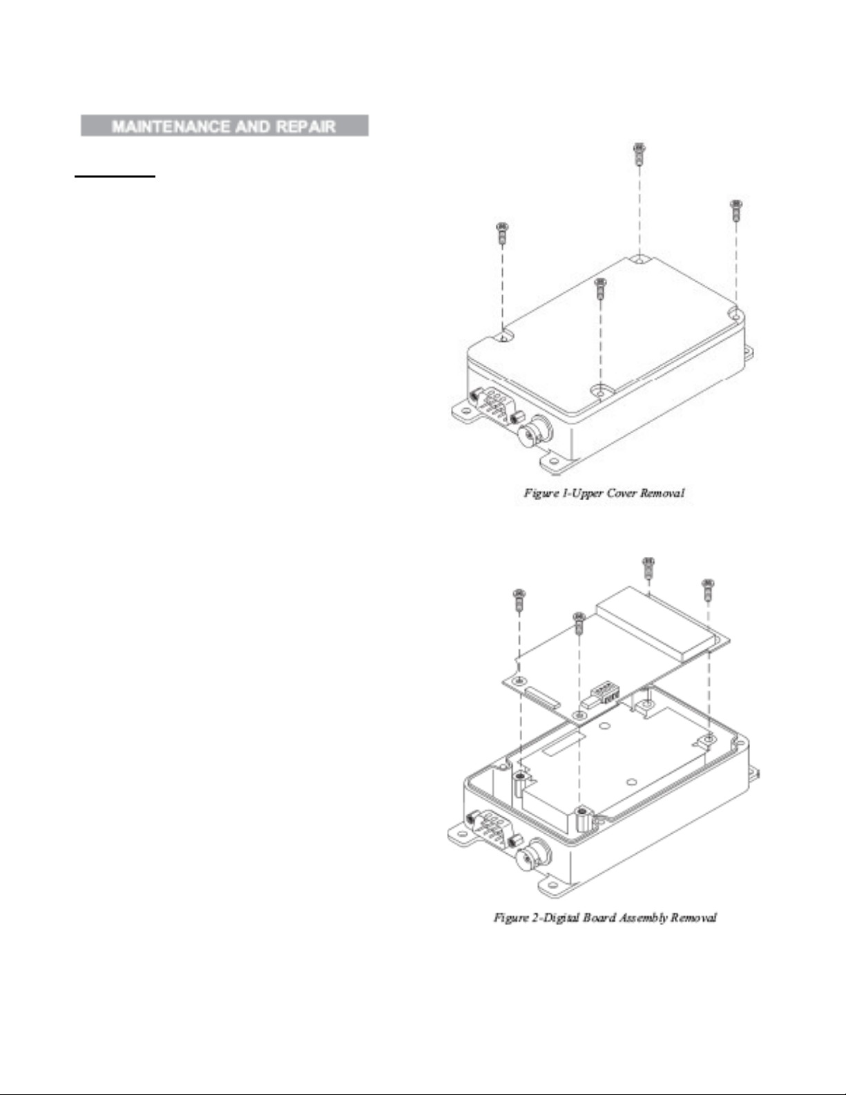
When removing or fitting, use the Exploded View and Parts
List, located on page 55 in conjunction with the following
procedures:
• WARNING: Disconnect the SD-125 from all
external equipment at the D-Sub connector prior to
disassembly.
REMOVING & REPLACING THE UPPER
COVER
Removing the Upper Cover:
1. Unscrew the four upper cover mounting screws
located on the upper cover of the radio.
To replace the Upper Cover:
1. Reverse the steps taken to remove the Upper
Cover.
REMOVING & REPLACING THE DIGITAL
BOARD & SHIELD PLATE
Removing the Digital Board Assembly & Shield
Plate:
1. Remove the Upper Cover (refer to Removing &
Replacing the Upper Cover).
2. Disconnect the DB9 pin connector on CON401.
3. Unscrew the 4 mounting screws.
4. Remove the Digital Board Assembly.
5. Remove the Shield Plate.
To replace the Digital Board Assembly:
1. Reverse the steps taken to remove the Digital
Board Assembly & Shield Plate.
PAGE-10-
October 98
MAXON
SD-125 RF LINK MODULE
Page 14
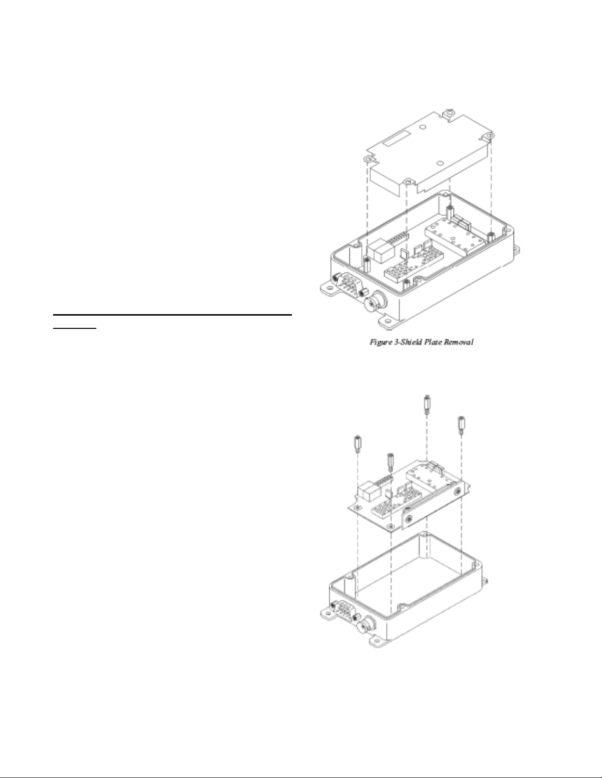
REMOVING & REPLACING THE RF
BOARD
Removing the RF Board Assembly:
1. Remove the Upper Cover (refer to Removing &
Replacing the Upper Cover).
2. Remove the Digital Board Assembly and Shield
Plate (refer to Removing & Replacing the Digital
Board Assembly & Shield Plate).
3. Unscrew the 4 mounting standoffs.
4. Unsolder the antenna connector cable.
5. Remove the RF Board Assembly.
To replace the RF Board Assembly:
1. Reverse the steps taken to remove the RF Board
Assembly.
PAGE-11-
October 98
MAXON
SD-125 RF LINK MODULE
Figure 4-RF Board Removal
Page 15

MAXON
SD-125 RF LINK MODULE
The SD-125 Series radio requires the ACC-900
Programming Software, ACC-2000 Interface Module,
9-15 VDC 200mA Power Supply and QPA-4000
Programmer Interface Cable.
Refer to the ACC-900 Programming Manual (P/N: 680110-0032) for detailed information on programming the
SD-125 Series radio.
PAGE-12-
October 98
The SD-125 UHF/VHF Receiver is by design, broad
band covering UHF(400-430 MHz & 440-470 MHz)
and VHF(148-174 MHz) and should require no
special alignment, unless repairs are performed on
the receiver portion.
Should repairs be necessary, use the "Test
Equipment Diagram" on page 17 & the "Alignment
Points Diagram" on page 18, in conjunction with the
following procedures:
• An Extender Board (P/N: 650-060-0016) is
required in order to separate the Digital and
RF PCB.s to allow access to the alignment
points. Installation instructions are provided
with the Extender Board Assembly.
RECEIVER
1. Apply a standard test signal to the receiver
antenna terminals.
2. Adjust T1 for maximum sensitivity and audio
output with minimum audio distortion.
3. Adjust RV403 for the specific audio output
level.
RX VCO
1. Set the unit to the highest receive frequency,
470MHz(UHF), 174MHz(VHF) and adjust
the VCO L303 to 8 volts.
2. Set the unit to the lowest receive frequency
440MHz(UHF), 148(VHF) and check that the
VCO voltage is above 2.0 volts. If voltage is
below 2.0 volts, adjust L303 for 2.0 volts or
more.
• Note: Use TP1 to measure the voltage.
TRANSMITTER
Connect the unit to a Service Monitor with the power
meter setting to the 10 W scale (or autorange)
TCXO
Set the channel selector to the mid-range frequency
460 MHz, adjust TCX01 for a reading of 460 MHz
±200Hz (155 MHz VHF models).
Page 16

TX VCO
1. Set the unit to the highest transmit frequency,
470MHz(UHF), 174MHz(VHF) key the
transmitter and adjust the VCO L203 to 8
volts.
2. Set the unit to the lowest transmit frequency
440 MHz(UHF), 148(VHF) key the transmitter
and check that the VCO voltage is above 2.0
volts. If voltage is below 2.0 volts, adjust L203
for 2.0 volts or more.
Note: use TP1 to measure the voltage.
TX Deviation and Balance Adjustment
1. Set the unit to a mid-frequency and input the
TX data with 400 Hz standard audio level.
2. Increase the signal level to 20 dB from
standard level.
3. Monitor the demodulated signal from service
monitor. Adjust RV3 to make the monitored
signal to be a balanced square wave.
4. Reduce input signal to the standard level and
adjust RV2 for the standard deviation.
APC
1. Adjust RV1 for High Power (5W)
2. Adjust RV6 for Low Power (1W)
3. This completes the transmitter alignment
procedures.
SD-125 Squelch setting using the ACC-2000
Interface Module
Maxon.s wide range of data radio products since the
crystal control module (DM-0500 series) had their
squelch level setting by hardware touch up. With the
new SD-125 series, the squelch level to open or close
(unmute or mute) is set up by software control.
The RSSI utilizes the A/D conversion that will be fed to
the microprocessor, which in turn will use this input to
determine the squelch level setting to control the mute
and unmute of the receiver.
Default setting of squelch level for all the SD-125 from
our manufacture and workshop is approximately set at:
PAGE-13-
October 98
MAXON
SD-125 RF LINK MODULE
1. Squelch open (unmute) at -114dBm to 113dBm (0.45 - 0.5mV of the RX signal
strength)
2. Squelch close (mute) at -117dBm to 116dBm (0.3 - 0.35mV of the RX signal
strength)
Changing the default squelch settings requires use
of the programming adaptor box. This box is
designed for use not only as part of the
programming kit but also as a tool of squelch level
setting.
The minimum equipment required for squelch level
setting is a RF signal generator. Radio
communication test equipment is recommended.
1. Power up the programming adaptor box (use the
DC supply of 9 - 15 Volts 200mA).
2. Hook up the SD-125 unit to the programming
adaptor box, and its antenna connector to the RF
input port of the RF signal generator.
3. With the adaptor box turned "off., simultaneously
press and hold both "ON/OFF" and "WRITE" buttons
down.
4. Release the "ON/OFF" button first then the
"WRITE" button next. (LED indicator on the box will
flash twice after that it may stay on / off, this is of no
concern , because depending on the signal strength
of the RF generator as well as the pre-set level of
squelch the SD125 may be in standby mode (LED
OFF) or in receiving mode (LED ON)
5. Adjust the RF signal generator for the desired
signal strength to OPEN squelch (e.g. default setting
is -113dBm, that is equivalent to 0.5mV)
6. Press and release "READ" button, LED indicator
will flash 3 times then it will be ON.
7. Adjust the RF signal generator for the desired
signal strength to CLOSE squelch (e.g. default
setting is -116dBm, that is equivalent to 0.35mV)
8. Press and release "READ" button, LED indicator
will flash 1 time then it will be OFF.
9. Press and release "WRITE" button, LED indicator
will flash twice.
10. Squelch level is now set. Test for desired level
by increasing or decreasing the RF signal to levels
set
Page 17

for open and close squelch (mute LED will be OFF &
unmute LED will be ON).
NOTE: The difference of RF signal strength
between the unmute and mute levels must be
greater than or at least equal to 0.15mV (i.e. at
least -123.5dBm) for the squelch setting to
work properly. If they are too close to one
another, RSSI through the A/D conversion can
not differentiate between the mute and unmute
level properly. As a result, it would cause the
CD (Carrier Detect) to act intermittently.
PAGE-14-
October 98
MAXON
SD-125 RF LINK MODULE
Page 18

MAXON
SD-125 RF LINK MODULE
PAGE-15-
October 98
Page 19

MAXON
SD-125 RF LINK MODULE
PAGE-16-
October 98
Page 20

COMPONENT REPLACEMENT
COMPONENT REPLACEMENT
Surface Mount Components
Surface mount components should always be replaced using
a temperature controlled soldering system. The soldering
tools may be either a temperature controlled soldering iron or
a temperature controlled hot-air soldering station. A hot-air
system is recommended for the removal of components on
these boards. With either soldering system, a temperature
of 700 F (371 C) should be maintained.
The following procedures outline the removal and
replacement of surface mount components. If a hot-air
soldering system is employed, see the manufacturer s
operating instructions for detailed information on the use of
your system.
CAUTION: Avoid applying heat to the body of any
surface mount component using standard soldering
methods. Heat should be applied only to the
metalized terminals of the components. Hot-air
systems do not damage the components since the
heat is quickly and evenly distributed to the external
surface of the component
CAUTION: The CMOS Integrated Circuit devices
used in this equipment can be destroyed by static
discharges. Before handling one of these devices,
service technicians should discharge themselves by
touching the case of a bench test instrument that
has a 3-prong power cord connected to an outlet
with a known good earth ground. When soldering
or desoldering a CMOS device, the soldering
equipment should have a known good earth
ground.
Surface Mount Removal
1 . Grip the component with tweezers or small needle
nose pliers.
2. Alternately heat the metalized terminal ends of
the surface mount component with the soldering
iron. If a bot-air system is used, direct the heat to
the terminals of the component Use extreme care
with the soldering equipment to prevent damage
to the printed circuit board (PCB) and the
surrounding components.
3. When the solder on all terminals is liquefied,
gently remove the component Excessive force
may cause the PCB pads to separate from the
board if all solder is not completely liquefied.
4. lt may be necessary to remove excess solder
using a vacuum de-soldering tool or Solder wick.
Again, use great care when de-soldering or
soldering on the printed circuit boards. It may also
be necessary to remove the epoxy adhesive that
was under the
PAGE - 17
October 98
MAXON
SD-125 RF LINK MODULE
surface mount component and any flux on the printed
circuit board.
Surface Mount Component Replacement
1 . Tin one terminal end of the new component and
the corresponding pad of the PCB. Use as little
solder as possible.
2. Place the component on the PCB pads,
observing proper polarity for capacitors, diodes,
transistors, etc.
3. Simultaneously touch the tinned terminal end
and the tinned pad with the soldering iron.
Slightly press the component down on the
board as the solder liquefies. Solder all
terminals, allowing the component time to cool
between each application of heat. Do not apply
heat for an excessive length of time and do not
use excessive solder.
With a hot-air system, apply hot air until all tinned areas
are melted and the component is seated in place. lt may
be necessary to slightly press the component down on the
board. Touch up the soldered connections with a standard
soldering iron if needed. Do not use excessive solder.
• CAUTION: Some chemicals may damage the
internal and external plastic parts of the radio.
4. Allow the component and the board to cool and
then remove all flux from the area using alcohol
or another approved flux remover.
Surface Mounted Integrated Circuit
Replacement
Soldering and de-soldering techniques of the surface
mounted IC s are similar to the above outlined procedures
for the surface mounted chip components. Use extreme
care and observe static precautions when removing or
replacing the defective (or suspect) IC s. This will prevent
any damage to the printed circuit board or the surrounding
circuitry.
The hot-air soldering system is the best method of
replacing surface mount IC s. The IC s can easily be
removed and installed using the bot-air system. See the
manufacturer s instructions for complete details on tip
selection and other operating instructions unique to your
system. If a hot-air system is not available, the service
technician may wish to clip the pins near the body of the
defective IC and remove it. The pins can then be removed
from the PCB with a standard soldering iron and tweezers,
and the new IC installed following the Surface Mount
Component Replacement procedures. it may not be
necessary to tin all (or any) of the IC pins before the
installation process.
Page 21

MAXON
SD-125 RF LINK MODULE
SIMPTOMS CAUSES COUNTERMEASURES
Unit does not work
Bad RX Sensitivity
(-10 to -60d B)
Defective RX
1. lncomplete connection
2. Defective DC/DC VCC
3. Sv voltage source
4. PLL error
5. Filtering error
6. EEPROM fail
1. Defective ANT Switch
2. Defective Front-End
3. Defective dBm
4. IF IC
5. VCO levei drop
6. Change of 1 St local f requency
1. VCO frequency change or level drop
2. Defective voltage source
1. Check CON401 connection
2. Check U801
3. 1C1 (Sv -0.2v)
4. Check TCXOIVCO/PLL IC
5. Check LPF (IC407)
6. Re-programming
1. Check D5, D6
2. Check Q601
3. Check D9, T2, T3
4. Replace 1C5
5. RX VCO level.2dBm
6. Re-Tune TCXO
1. Repair RX VCO
2. Defective IF IC (ICS)
3. [Cl, Ql, Q3
PLL Error
Low TX Power
No TX Power
No Modulation
No Programming
• An Extender Bard, P/N: 650-060-0016, is required in order to separate the Digital and RF PCB s for
troubleshooting purposes.
1. Defective 12.8 MHz TCXO
2. Voltage source for RX VCPITX VCO
3. Defective PLL IC
1. APC 1. Re-adjust Rvi
1. TX Buffer
2. Power Module
3. APC controf
1. SW IC & Mic Amp [C 1. Check U404, 405, 406
1. Short protector VCC 1. Defective programming lead
PAGE-18-
October 98
1. Replace TCXO
2. Check RX VCO/TX VCO
3. Replace 1C2
1. Check Ql 6, 17
2. Check Q501, 502, 503
3. Check Q22, D4
Page 22

SD-125 RF LINK MODULE
CONTROL CIRCUIT TRANSISTOR
RX TX
REF# B C E B C E
Q401 5,0 0,0 5,0
5,0 0,0 5,0
Q402 5,0 GND 5,0 5,0 0.0 5,0
Q403 4.7 0,0 5,0 4.7 0,0 5,0
Q404 4.8 0,0 GND - 0,0 GND
Q405 4.6 1.8 1.8 4.6 1.8 1.8
Q406 4.8 0,0 0.0 0.0 5,0 0.0
Q407 7.5 4,0 7.5 7.5 4,0 7.5
Q408 0.0 7.5 0.0 0.0 7.5 0.0
RF BOARD TRANSISTOR
RX TX
REF# B C E B C E
Q2
Q3 0.0 4.7 5.0 4.7 0.0 5.0
Q4 0.0 5.0 5.0 0.0 5.0 5.0
Q5 5.0 0.0 5.0 5.0 0.0 5.0
Q6 4.0 18.0 5.0 4.2 18.0 5.0
Q7 18.0 6.3 18.0 18.0 6.3 18.0
Q8 5.0 0.0 5.0 5.0 0.0 5.0
Q11 0.0 6.3 0.0 0.0 6.3 0.0
Q12 2.0 4.7 1.2 0.0 0.0 0.0
Q13
Q14 0.0 0.0 0.0 4.6 4.6 4.6
Q16 0.0 0.0 0.0 1.6 4.8 0.8
Q17 0.0 0.0 0.0 0.6 3.0 GND
Q18 0.0 0.0 0.0 5.0 0.2 GND
Q19 1.0 7.5 0.5 1.6 7.5 1.0
Q21 0.0 7.5 0.0 1.6 6.6 1.2
Q22 7.5 0.0 7.5 6.8 5.0 7.5
Q25 0.7 4.0 GND
4.7 0.0 5.0 0.0 4.7 5.0
4.6 4.6 4.0 0.0 0.0 0.0
0.0 0.0 GND
PAGE-19-
October 98
MAXON
Page 23

SD-125 RF LINK MODULE
RF BOARD IC´S
RECEIVE MODE
Pin # IC1 IC2 IC3(OFF) IC5 IC7(OFF) IC8(OFF)
1 GND NC
2 GND 5.0
3 GND 5.0
4
5.0
5.0
5 GND 5.0
6
7
8
9
10
11
12
13
14
15
16
17
18
19
20
7.5
-
-
-
-
-
-
-
-
-
-
-
-
-
-
NC
GND
NC
NC
AUDIO
AUDIO
5.0
NC
5.0
0.0
0.0
4.6
0.0
4.7
0SC1
-
-
-
-
-
-
-
-
-
-
-
-
-
-
-
-
-
-
-
-
OSC1
0SC2
-
4.7
3.3
3.3
3.3
4.7
AUDIO
NC
NC
NC
-
NC
GND
1.8
-
-
-
-
- -
- -
- -
- -
- -
- -
- -
- -
- -
- -
- -
- -
- -
- -
- -
- -
- -
- -
- -
- -
RF BOARD IC’S
TRANSMIT MODE
Pin # IC1 IC2 IC3(OFF) IC5(OFF) IC7 IC8(OFF)
1 GND NC
2 GND 5.0
3 GND 5.0
4
5.0
5 GND 5.0
6
7
8
9
10
11
12
13
14
15
16
17
18
19
20
7.5
-
-
-
-
-
-
-
-
-
-
-
-
-
-
5.0
NC
GND
NC
NC
AUDIO
AUDIO
5.0
NC
5.0
0.0
5.0
4.6
0.0
4.7
0SC1
1.6 - 1.8
3.0 - 1.8
3.0 - 1.8
GND - GND
0.8 - 1.8
0.3 - 1.8
4.0 - 1.8
5.0 - 5.0
- - -
- - -
- - -
- - -
- - -
- - -
- - -
- - -
- - -
- - -
- - -
- - -
PAGE-20-
October 98
MAXON
0.7
0.3
0.3
GND
1.88
1.88
1.88
5.0
Page 24

SD-125 RF LINK MODULE
CONTROL CIRCUIT IC’S
RECEIVE MODE
PIN #
1 0.0 1.3 - - 1.8 AUDIO
2 0.0 0.0 - - 1.8 GND
3 0.7 5.0 - - 1.8 AUDIO
4 5.0 1.8 - - 5.0 GND
5 GND 2.0 GND - AUDIO AUDIO
6 4.7 5.0 0.0 - 1.8 7.5
7 4.7 0.3 1.8 - AUDIO 4.0
8 4.7 0.0 1.8 AUDIO - AUDIO
9 - 1.8 - AUDIO -
10 - AUDIO 0.0 1.8 -
11 - AUDIO 0.0 AUDIO -
12 - GND 5.0 AUDIO -
13 - - - - -
14 - - - - -
15 - - - - -
16 - - - - -
17 - - - - -
18 - - - - -
19 - - - - -
20 - - - - -
PIN #
1 4.63 23 4.7
2 4.63 24 4.7
3 0.0 25 4.7
4 5.0 26 0.0
5 0.0 27 5.0
6 0.0 28 4.6
7 2.0 29 GND
8 4.6 30 4.6
9 4.6 31 0.0
10 4.6 32 4.6
11 0.0 33 0.0
12 0.0 34 0.0
13 0.0 35 0.9
14 4.6 36 OSC2
15 4.7 37 OSC1
16 NC 38 7.5
17 GND 39 NC
18 5.0 40 NC
19 0.0 41 4.6
20 0.0 42 4.6
21
22 N.C
IC402 IC403 IC404 IC405 IC406 IC407 IC408
IC401
0.0
PIN #
43
44 0.0
PAGE-21-
October 98
IC401
GND
MAXON
Page 25

CONTROL CIRCUIT IC’S
TRANSMIT MODE
PIN #
1 0.0
2 0.0
3 4.7
4
5 GND
6
7
8
9
10
11
12
13
14
15
16
17
18
19
20
PIN #
1 0.0 23 4.7
2 0.0 24 4.7
3 4.6 25 4.7
4 5.0 26 0.0
5 0.0 27 5.0
6 0.0 28 4.6
7 4.6 29 GND
8 4.6 30 4.6
9 4.6 31 0.0
10 0.0 32 4.6
11 0.0 33 0.0
12 0.0 34 0.0
13 4.6 35 0.0
14 0.4 36 OSC2
15 0.4 37 OSC1
16 NC 38 4.6
17 GND 39 NC
18 5.0 40 NC
19 0.0 41 4.6
20 0.0 42 4.6
21
22 0.0
IC402 IC403 IC404 IC405 IC406 IC407 IC408
- - AUDIO 1.8 -
- - AUDIO 1.8 -
- AUDIO AUDIO 1.8 -
5.0 - AUDIO 5.0 5.0 -
- 0.0 AUDIO - -
4.7 - - AUDIO - -
4.7 - GND AUDIO - -
4.7 - - 1.8 AUDIO -
-
-
-
-
- - - 1.8 AUDIO -
- - - 1.8 AUDIO -
- - - - - -
- - - - - -
- - - - - -
- - - - - -
- - - - - -
- - - - - -
IC401
-
-
-
-
- 1.8 AUDIO
AUDIO 1.8 1.8
AUDIO GND GND
4.6 0.0 1.8
PIN #
4.7
43
44 0.0
PAGE-22-
October 98
MAXON
SD-125 RF LINK MODULE
-
-
-
-
IC401
GND
Page 26

SD-125 RF LINK MODULE
MAXON
REF # DESCRIPTION _________ PART #
C401 CAP, CER,1UF,+80-20%,16V,Y5V,0805 100-803-2105
C402 CAP, CER,0.001UF,10%,50V,X7R,0603 100-621-1102
C403 CAP, CER,0.022UF,10%,50V,X7R,0603 100-621-1223
C404 CAP, CER,0.1UF,+80-20%,25V,Y5V,0603 100-813-1104
C405 CAP, CER,47PF,5%,50V,COG,0603 100-520-1470
C406 CAP, CER,0.022UF,10%,50V,X7R,0603 100-621-1223
C407 CAP, CER,0.1UF,+80-20%,25V,Y5V,0603 100-813-1104
C408 CAP, CER,47PF,5%,50V,COG,0603 100-520-1470
C409 CAP, CER,0.047UF,+20-80%,25V,Y5V,0603 100-813-1473
C410 CAP, CER,0.0056UF,10%,50V,X7R,0603 100-621-1562
C411 CAP, CER,0.0027UF,5%,50V,X7R,0603 100-521-1272
C412 CAP, CER,0.0047UF,10%,50V,X7R,0603 100-621-1472
C413 CAP, CER,150PF,10%,50V,X7R,0603 100-621-1151
C414 CAP, CER,0.0039UF,10%,50V,X7R,0603 100-621-1392
C415 CAP, CER,47PF,5%,50V,COG,0603 100-520-1470
C416 CAP, CER,0.1UF,+80-20%,25V,Y5V,0603 100-813-1104
C417 CAP, CER,0.1UF,+80-20%,25V,Y5V,0603 100-813-1104
C422 CAP, CER,0.1UF,+80-20%,25V,Y5V,0603 100-813-1104
C423 CAP, CER,0.047UF,+20-80%,25V,Y5V,0603 100-813-1473
C424 CAP, CER,470PF,10%,50V,X7R,0603 100-621-1471
C425 CAP, TA,10UF,20%,6.3V,3216,A 102-013-0106
C426 CAP, CER,0.047UF,+20-80%,25V,Y5V,0603 100-813-1473
C427 CAP, TA,100UF,20%,6.3V,D 102-013-3107
C428 CAP, TA,47UF,20%,16V,7343H 102-033-5476
C429 CAP, CER,0.001UF,10%,50V,X7R,0603 100-621-1102
C430 CAP, CER,0.001UF,10%,50V,X7R,0603 100-621-1102
C431 CAP, CER,0.001UF,10%,50V,X7R,0603 100-621-1102
C432 CAP, CER,0.001UF,10%,50V,X7R,0603 100-621-1102
C433 CAP, CER,0.001UF,10%,50V,X7R,0603 100-621-1102
C434 CAP, CER,0.001UF,10%,50V,X7R,0603 100-621-1102
C435 CAP, TA,4.7UF,20%,10V,A 102-023-0475
C436 CAP, CER,0.1UF,+80-20%,25V,Y5V,0603 100-813-1104
C437 CAP, CER,39PF,5%,50V,COG,0603 100-520-1390
C438 CAP, CER,39PF,5%,50V,COG,0603 100-520-1390
C439 CAP, TA,1UF,20%,25V,3216 102-053-0105
C440 CAP, TA,10UF,20%,6.3V,3216,A 102-013-0106
C441 CAP, CER,0.001UF,10%,50V,X7R,0603 100-621-1102
C442 CAP, CER,0.001UF,10%,50V,X7R,0603 100-621-1102
C443 CAP, CER,0.001UF,10%,50V,X7R,0603 100-621-1102
C444 CAP, CER,0.001UF,10%,50V,X7R,0603 100-621-1102
C445 CAP, CER,0.001UF,10%,50V,X7R,0603 100-621-1102
C446 CAP, CER,0.001UF,10%,50V,X7R,0603 100-621-1102
C447 CAP, TA, 22UF,20%,35V,7343 102-063-3226
C449 CAP, CER,0.001UF,10%,50V,X7R,0603 100-621-1102
C450 CAP, CER,0.1UF,+80-20%,25V,Y5V,0603 100-813-1104
C451 CAP, CER,0.01UF,10%,25V,X7R,0603 100-611-1103
C452 CAP, CER,0.001UF,10%,50V,X7R,0603 100-621-1102
C453 CAP, CER,0.1UF,+80-20%,25V,Y5V,0603 100-813-1104
C454 CAP, TA,4.7UF,20%,10V,A 102-023-0475
C455 CAP, TA,4.7UF,20%,10V,A 102-023-0475
C456 CAP, TA,4.7UF,20%,10V,A 102-023-0475
C457 CAP, TA,4.7UF,20%,10V,A 102-023-0475
C458 CAP, CER,47PF,5%,50V,COG,0603 100-520-1470
C459 CAP, CER,47PF,5%,50V,COG,0603 100-520-1470
C460 CAP, TA,10UF,20%,6.3V,3216,A 102-013-0106
C461 CAP, TA,1UF,20%,25V,3216 102-053-0105
REF # DESCRIPTION ________________ ____PART #
C463 CAP, CER,0.1UF,+80-20%,25V,Y5V,0603 100-813-1104
C464 CAP, CER,0.1UF,+80-20%,25V,Y5V,0603 100-813-1104
C465 CAP, CER,0.0033UF,10%,50V,X7R,0603 100-621-1332
C466 CAP, CER,0.0027UF,5%,50V,X7R,0603 100-521-1272
C801 CAP, CER,51PF,5%,50V,COG,0603 100-520-1510
C802 CAP, CER,0.1UF,+80-20%,25V,Y5V,0603 100-813-1104
C803 CAP, CER,330PF,5%,50V,COG,0603 100-520-1331
C804 CAP, CER,51PF,5%,50V,COG,0603 100-520-1510
C805 CAP, CER,100PF,+/-5%,50V,COG,0603 100-520-1101
C806 CAP, CER,100PF,+/-5%,50V,COG,0603 100-520-1101
C807 CAP, TA, 22UF,20%,35V,7343 102-063-3226
C808 CAP, CER,0.1UF,+80-20%,25V,Y5V,0603 100-813-1104
C810 CAP, CER,0.01UF,10%,25V,X7R,0603 100-611-1103
C811 CAP, TA,100UF,20%,16V,E,7343 102-033-3107
C812 CAP, CER,100PF,+/-5%,50V,COG,0603 100-520-1101
C813 CAP, TA,4.7UF,20%,10V,A 102-023-0475
C815 CAP, TA,100UF,20%,16V,E,7343 102-033-3107
CON401 CONN,PLUG,15P,1.25MM,RT,SMT 140-081-0015
CON403 CONN, SKT,18P/DIP,2.0MMST,SMT 140-020-0056
D401 DIODE, ZNR,Z02W5.6V-Y,5.6V,0.2W,SOT-23 221-020-0056
D402 DIODE, ZNR,Z02W5.6V-Y,5.6V,0.2W,SOT-23 221-020-0056
D403 DIODE, ZNR,Z02W5.6V-Y,5.6V,0.2W,SOT-23 221-020-0056
D404 DIODE, ZNR,Z02W5.6V-Y,5.6V,0.2W,SOT-23 221-020-0056
D405 DIODE, ZNR,Z02W5.6V-Y,5.6V,0.2W,SOT-23 221-020-0056
D406 DIODE, SW ,KDS193,SOT-23 220-010-0003
D407 DIODE, ZNR,Z02W5.6V-Y,5.6V,0.2W,SOT-23 221-020-0056
D408 DIODE, ZNR,Z02W5.6V-Y,5.6V,0.2W,SOT-23 221-020-0056
D409 DIODE, ZNR,Z02W5.6V-Y,5.6V,0.2W,SOT-23 221-020-0056
D410 DIODE, ZNR,Z02W5.6V-Y,5.6V,0.2W,SOT-23 221-020-0056
D801 DIODE, SW ,KDS160,6V,2PIN USC 220-010-0017
D802 DIODE, SCHOTTKY,MBRS140T3,SMB 220-040-0012
L801 COIL, CHIP,12UH, A814AY-120M=P3 355-010-0120
L802 COIL, CHIP,3.3UH, 636CY-3R3M=P3 355-010-0335
Q401 TRANS, PNP,KRA104S,SOT-23,SW,(PD) 870-010-0005
Q402 TRANS, PNP,KRA104S,SOT-23,SW,(PD) 870-010-0005
Q403 TRANS, PNP,KRA104S,SOT-23,SW,(PD) 870-010-0005
Q404 TRANS, NPN,KRC104SND,SOT-23,SW,ND 870-020-0001
Q405 TRANS, PNP,KRA104S,SOT-23,SW,(PD) 870-010-0005
Q406 TRANS, NPN,KRC104SND,SOT-23,SW,ND 0-020-0001
Q407 TRANS, PNP,KTA1504(Y),SOT-23,SW 870-100-0004
Q408 TRANS, NPN,KRC104SND,SOT-23,SW,ND 870-020-0001
Q801 TRANS, SI4412DY,SO-8,MOSFET,N-CH 870-070-0006
Q802 TRANS, SI4412DY,SO-8,MOSFET,N-CH 870-070-0006
R403 RES, TF,10K,5%,1/16W,+/-200,0603 741-102-1103
R404 RES, TF,47K,5%,1/16W,+/-200,0603 741-102-1473
R406 RES, TF,22K,5%,1/16W,+/-200,0603 741-102-1223
R407 RES, TF,10K,5%,1/16W,+/-200,0603 741-102-1103
R409 RES, TF,100K,5%,1/16W,+/-200,0603 741-102-1104
R410 RES, TF,220K,5%,1/16W,+/-200,0603 741-102-1224
R411 RES, TF,100K,5%,1/16W,+/-200,0603 741-102-1104
R412 RES, TF,3.3K,5%,1/16W,+/-200,0603 741-102-1332
R413 RES, TF,180K,5%,1/16W,+/-200,0603 741-102-1184
R414 RES, TF,100K,5%,1/16W,+/-200,0603 741-102-1104
R415 RES, TF,10K,5%,1/16W,+/-200,0603 741-102-1103
R416 RES, TF,10K,5%,1/16W,+/-200,0603 741-102-1103
R417 RES, TF,10K,5%,1/16W,+/-200,0603 741-102-1103
PAGE-23-
October 98
Page 27

REF # DESCRIPTION PART #
R418 RES, TF,10K,5%,1/16W,+/-200,0603 741-102-1103
R419 RES, TF,10K,5%,1/16W,+/-200,0603 741-102-1103
R420 RES, TF,9.1K,5%,1/16W,+/-200,0603 741-102-1912
R421 RES, TF,10K,5%,1/16W,+/-200,0603 741-102-1103
R422 RES, TF,10K,5%,1/16W,+/-200,0603 741-102-1103
R423 RES, TF,1K,5%,1/16W,+/-200,0603 741-102-1102
R424 RES, TF,10K,5%,1/16W,+/-200,0603 741-102-1103
R425 RES, TF,10K,5%,1/16W,+/-200,0603 741-102-1103
R426 RES, TF,10K,5%,1/16W,+/-200,0603 741-102-1103
R428 RES, TF,10K,5%,1/16W,+/-200,0603 741-102-1103
R429 RES, TF,47K,5%,1/16W,+/-200,0603 741-102-1473
R430 RES, TF,1M,5%,1/16W,+/-200,0603 741-102-1105
R431 RES, TF,47K,5%,1/16W,+/-200,0603 741-102-1473
R432 RES, TF,47K,5%,1/16W,+/-200,0603 741-102-1473
R433 RES, TF,4.7K,5%,1/16W,+/-200,0603 741-102-1472
R434 RES, TF,4.7K,5%,1/16W,+/-200,0603 741-102-1472
R435 RES, TF,10K,5%,1/16W,+/-200,0603 741-102-1103
R436 RES, TF,4.7K,5%,1/16W,+/-200,0603 741-102-1472
R437 RES, TF,10K,5%,1/16W,+/-200,0603 741-102-1103
R438 RES, TF,2.2K,5%,1/16W,+/-200,0603 741-102-1222
R439 RES, TF,4.7K,5%,1/16W,+/-200,0603 741-102-1472
R440 RES, TF,10K,5%,1/16W,+/-200,0603 741-102-1103
R441 RES, TF,47K,5%,1/16W,+/-200,0603 741-102-1473
R442 RES, TF,47K,5%,1/16W,+/-200,0603 741-102-1473
R443 RES, TF,47K,5%,1/16W,+/-200,0603 741-102-1473
R444 RES, TF,47K,5%,1/16W,+/-200,0603 741-102-1473
R445 RES, TF,100K,5%,1/16W,+/-200,0603 741-102-1104
R446 RES, TF,100,5%,1/16W,+/-200,0603 741-102-1101
R447 RES, TF,10K,5%,1/16W,+/-200,0603 741-102-1103
R448 RES, TF,1M,5%,1/16W,+/-200,0603 741-102-1105
R449 RES, TF,20K,5%,1/16W,+/-200,0603 741-102-1203
R450 RES, TF,33K,5%,1/16W,+/-200,0603 741-102-1333
R451 RES, TF,100K,5%,1/16W,+/-200,0603 741-102-1104
R452 RES, TF,100K,5%,1/16W,+/-200,0603 741-102-1104
R454 RES, TF,10K,5%,1/16W,+/-200,0603 741-102-1103
R455 RES, TF,22K,5%,1/16W,+/-200,0603 741-102-1223
R456 RES, TF,470,5%,1/16W,+/-200,0603 741-102-1471
R457 RES, TF,22K,5%,1/16W,+/-200,0603 741-102-1223
R458 RES, TF,100K,5%,1/16W,+/-200,0603 741-102-1104
R460 RES, TF,10K,5%,1/16W,+/-200,0603 741-102-1103
R461 RES, TF,10K,5%,1/16W,+/-200,0603 741-102-1103
R463 RES, TF,1.8M,5%,1/10W,+/-200,0805 741-112-2185
R464 RES, TF,47K,5%,1/16W,+/-200,0603 741-102-1473
R465 RES, TF,10K,5%,1/16W,+/-200,0603 741-102-1103
R466 RES, TF,47K,5%,1/16W,+/-200,0603 741-102-1473
R467 RES, TF,47K,5%,1/16W,+/-200,0603 741-102-1473
R468 RES, TF,10K,5%,1/16W,+/-200,0603 741-102-1103
R469 RES, TF,100K,5%,1/16W,+/-200,0603 741-102-1104
R470 RES, TF,100K,5%,1/16W,+/-200,0603 741-102-1104
R471 RES, TF,220K,5%,1/16W,+/-200,0603 741-102-1224
R472 RES, TF,120K,5%,1/16W,+/-200,0603 741-102-1124
R473 RES., TF,68K, 5%, 1/16W,+/-200, 0603 741-102-1683
R474 RES, TF,100,5%,1/16W,+/-200,0603 741-102-1101
R475 RES, TF,100,5%,1/16W,+/-200,0603 741-102-1101
R476 RES, TF,100,5%,1/16W,+/-200,0603 741-102-1101
R477 RES, TF,100,5%,1/16W,+/-200,0603 741-102-1101
R478 RES, TF,10K,5%,1/16W,+/-200,0603 741-102-1103
R480 RES, TF,100K,5%,1/16W,+/-200,0603 741-102-1104
R481 RES, TF,1K,5%,1/16W,+/-200,0603 741-102-1102
PAGE-24-
October 98
MAXON
SD-125 RF LINK MODULE
REF # DESCRIPTION PART #
R482 RES, TF,1K,5%,1/16W,+/-200,0603 741-102-1102
R483 RES, TF,1K,5%,1/16W,+/-200,0603 741-102-1102
R484 RES, TF,1K,5%,1/16W,+/-200,0603 741-102-1102
R485(LK2.10) RES, TF, 0, 5%,1/16W, +/-200,0603 741-102-1000
R486 RES., TF,68K, 5%, 1/16W,+/-200, 0603 741-102-1683
R487 RES, TF,10K,5%,1/16W,+/-200,0603 741-102-1103
R488 RES, TF,10K,5%,1/16W,+/-200,0603 741-102-1103
R489 RES, TF,10K,5%,1/16W,+/-200,0603 741-102-1103
R490 RES, TF,10,5%,1/16W,+/-200,0603 741-102-1100
R491 RES, TF,56K,5%,1/16W,+/-200,0603 741-102-1563
R492 RES, TF,100K,5%,1/16W,+/-200,0603 741-102-1104
R493 RES, TF,100K,5%,1/16W,+/-200,0603 741-102-1104
R494 RES, TF,100K,5%,1/16W,+/-200,0603 741-102-1104
R495 RES, TF,100K,5%,1/16W,+/-200,0603 741-102-1104
R496 RES, TF,0,5%,1/8W,TC250,1206 741-127-3000
R801 RES, TF,10K,5%,1/16W,+/-200,0603 741-102-1103
R802 RES, TF,36K,5%,1/16W,+/-200,0603 741-102-1363
R804 RES, TF,0.033,1%,1/10W,+/-100, 0805 740-112-R033
R805 RES, TF,68K,1%,1/16W,+/-100,0603 740-211-1683
R806 RES, TF,20K,5%,1/16W,+/-200,0603 741-102-1203
RV402 RES, TF,0, +/-5%,1/10W,+/-250,0805 741-117-2000
RV403 POT, VRES,22K,+/-25%,TOP ADJ 901-120-0223
RV404 RES, TF,0, +/-5%,1/10W,+/-250,0805 741-117-2000
SW401 SW, DIP8P,4 POS,KSD-04,SPST 830-130-0004
U401 IC, CPU, OPT, MC68HC705C8FB,44-QFP 443-100-0010
U402 IC, EEPROM,AT93C56-10SI,SO-8,2K,2-5V 442-010-0003
U403 IC, QUAD CMPTR,LM339,SO14 441-110-0003
U404 IC, SW/MUX,MC14066BDR2,SO-14,A-SW 444-050-0001
U405 IC, OP AMP,KIA324F,SO-14,QUAD 441-030-0002
U406 IC, OP AMP,KIA324F,SO-14,QUAD 441-030-0002
U407 IC, AUDIO AMP,LM386M-1,0.33W,SO-8 441-040-0002
U408 IC, V DET,KIA7042P,4.2V,SOT-89 441-020-0005
U801 IC, DC/DC CONV, LTC1435CS,SO-16 441-011-0005
X401 RESONATOR, CER,CSAC3.58MGC 310-020-0004
Page 28

SD-125 RF LINK MODULE
MAXON
REF # DESCRIPTION PART #
REPLACEMENT MODULES
ASSY, PCB,FRONT END,UHF,400-430MHZ 650-110-0019
ASSY, PCB,PWR AMP,UHF,400-430MHZ 650-230-0017
ASSY, PCB,TCXO 650-100-0002
ASSY, PCB,VCO TX/RX,UHF,400-430MHZ 650-030-0026
C1 CAP, CER,470PF,10%,50V,X7R,0603 100-621-1471
C2 CAP, TA,10UF,20%,6.3V,3216,A 102-013-0106
C3 CAP, CER,470PF,10%,50V,X7R,0603 100-621-1471
C4 CAP, CER,470PF,10%,50V,X7R,0603 100-621-1471
C5 CAP, CER,470PF,10%,50V,X7R,0603 100-621-1471
C6 CAP, TA,4.7UF,20%,10V,A 102-023-0475
C7 CAP, CER,470PF,10%,50V,X7R,0603 100-621-1471
C8 CAP, CER,470PF,10%,50V,X7R,0603 100-621-1471
C9 CAP, CER,470PF,10%,50V,X7R,0603 100-621-1471
C11 CAP, CER,0.1UF,+80-20%,25V,Y5V,0603 100-813-1104
C12 CAP, TA,10UF,20%,6.3V,3216,A 102-013-0106
C13 CAP, CER,0.01UF,10%,25V,X7R,0603 100-611-1103
C14 CAP, CER,470PF,10%,50V,X7R,0603 100-621-1471
C15 CAP, CER,0.1UF,+80-20%,25V,Y5V,0603 100-813-1104
C16 CAP, CER,2PF,0.25PF,50V,COG,0603 100-020-1020
C17 CAP, CER,0.1UF,+80-20%,25V,Y5V,0603 100-813-1104
C18 CAP, CER,0.001UF,10%,50V,X7R,0603 100-621-1102
C19 CAP, CER,220PF,5%,50V,COG,0603 100-520-1221
C21 CAP, METAL,POLY,0.33UF,63V BOX 083-013-2334
C22 CAP, METAL POLY,0.022UF,10%,63V BOX 083-013-2223
C23 CAP, METAL POLY,0.01UF,10%,63V KBOX 083-014-2103
C24 CAP, METAL POLY,0.01UF,10%,63V KBOX 083-014-2103
C25 CAP, CER,1UF,+80-20%,16V,Y5V,0805 100-803-2105
C26 CAP, CER,0.1UF,+80-20%,25V,Y5V,0603 100-813-1104
C34 CAP, CER,220PF,5%,50V,COG,0603 100-520-1221
C35 CAP, CER,470PF,10%,50V,X7R,0603 100-621-1471
C36 CAP, CER,7PF,0.5PF,50V,COG,0805 100-110-2070
C37 CAP, CER,5.6PF,0.25PF,50V,COG,0603 100-020-15R6
C38 CAP, CER,15PF,5%,50V,COG,0805 100-520-2150
C39 CAP, CER,470PF,10%,50V,X7R,0603 100-621-1471
C41 CAP, CER,6PF,0.5PF,50V,COG,0805 100-120-2060
C42 CAP, CER,27PF,5%,50V,COG,0805 100-520-2270
C43 CAP, CER,5PF,0.25PF,50V,COG,0603 100-020-1050
C44 CAP, CER,1UF,+80-20%,16V,Y5V,0805 100-803-2105
C45 CAP, CER,220PF,5%,50V,COG,0603 100-520-1221
C46 CAP, CER,3PF,0.25PF,50V,COG,0603 100-020-1030
C47 CAP, CER,220PF,5%,50V,COG,0603 100-520-1221
C49 CAP, CER,4.7PF,0.5PF,50V,COG,0805 100-120-24R7
C50 CAP, CER,12PF,5%,50V,COG,0603 100-520-1120
C51 CAP, CER,6.8PF,0.5PF,50V,COG,0603 100-120-16R8
C53 CAP, CER,1UF,+80-20%,16V,Y5V,0805 100-803-2105
C54 CAP, CER,220PF,5%,50V,COG,0603 100-520-1221
C55 CAP, CER,470PF,10%,50V,X7R,0603 100-621-1471
C56 CAP, CER,6.8PF,0.5PF,50V,COG,0603 100-120-16R8
C57 CAP, CER,470PF,10%,50V,X7R,0603 100-621-1471
C58 CAP, CER,470PF,10%,50V,X7R,0603 100-621-1471
C59 CAP, CER,0.47UF,+20-80%,16V,Y5V,0805 100-803-2474
C60 Cap, TA,4.7uF,20%,10V,A 102-023-0475
NOTES:
1. Components are not available, assembly is non-repairable.
REF # DESCRIPTION _______ PART #
C61 CAP, TA,10UF,20%,6.3V,3216,A 102-013-0106
C62 CAP, CER,470PF,10%,50V,X7R,0603 100-621-1471
C63 CAP, CER,0.01UF,10%,25V,X7R,0603 100-611-1103
C64 CAP, CER,470PF,10%,50V,X7R,0603 100-621-1471
C65 CAP, TA,10UF,20%,10V,B,3528 102-023-1106
C66 CAP, CER,470PF,10%,50V,X7R,0603 100-621-1471
C67 CAP, CER,470PF,10%,50V,X7R,0603 100-621-1471
C68 CAP, CER,470PF,10%,50V,X7R,0805 100-621-2471
C73 CAP, CER,9PF,0.25PF,50V,COG,0805 100-020-2090
C74 CAP, CER,18PF,5%,50V,COG,0805 100-520-2180
C75 CAP, CER,4PF,0.25PF,50V,COG,0805 100-020-2040
C76 CAP, CER,1PF,0.25PF,50V,COG,0805 100-020-2010
C77 CAP, CER,470PF,10%,50V,X7R,0805 100-621-2471
C78 CAP, CER,470PF,10%,50V,X7R,0603 100-621-1471
C79 CAP, CER,0.1UF,10%,25V,X7R,0805 100-611-2104
C80 CAP, CER,470PF,10%,50V,X7R,0603 100-621-1471
C81 CAP, CER,470PF,10%,50V,X7R,0603 100-621-1471
C82 CAP, CER,470PF,10%,50V,X7R,0603 100-621-1471
C83 CAP, CER,7PF,0.5PF,50V,COG,0603 100-120-1070
C84 CAP, CER,470PF,10%,50V,X7R,0603 100-621-1471
C87 CAP, CER,9PF,0.5PF,50V,COG,0603 100-120-1090
C88 CAP, CER,0.1UF,+80-20%,25V,Y5V,0603 100-813-1104
C90 CAP, CER,7PF,0.5PF,50V,COG,0603 100-120-1070
C92 CAP, CER,24PF,5%,50V,COG,0603 100-520-1240
C93 CAP, CER,82PF,5%,50V,COG,0603 100-520-1820
C94 CAP, CER,1UF,+80-20%,16V,Y5V,0805 100-803-2105
C96 CAP, CER,0.01UF,10%,25V,X7R,0603 100-611-1103
C97 CAP, CER,30PF,5%,50V,COG,0603 100-520-1300
C98 CAP, CER,0.001UF,10%,50V,X7R,0603 100-621-1102
C100 CAP, TA,10UF,20%,6.3V,3216,A 102-013-0106
C101 CAP, TA,10UF,20%,6.3V,3216,A 102-013-0106
C102 CAP, CER,0.001UF,10%,50V,X7R,0603 100-621-1102
C103 CAP, CER,470PF,10%,50V,X7R,0603 100-621-1471
C104 CAP, TA,1UF,20%,25V,3216 102-053-0105
C111 CAP, CER,470PF,10%,50V,X7R,0603 100-621-1471
C117 CAP, CER,47PF,5%,50V,COG,0603 100-520-1470
C118 CAP, CER,33PF,5%,50V,COG,0603 100-520-1330
C121 CAP, CER,20PF,5%,50V,COG,0603 100-520-1200
C122 CAP, CER,0.01UF,10%,25V,X7R,0603 100-611-1103
C123 CAP, CER,0.01UF,10%,25V,X7R,0603 100-611-1103
C124 CAP, CER,0.1UF,10%,25V,X7R,0805 100-611-2104
C125 CAP, CER,0.1UF,10%,25V,X7R,0805 100-611-2104
C126 CAP, CER,0.01UF,10%,25V,X7R,0603 100-611-1103
C127 CAP, CER,0.01UF,10%,25V,X7R,0603 100-611-1103
C128 CAP, TA,4.7UF,20%,10V,A 102-023-0475
C129 CAP, ELE,10UF,16V,20%,3X5,5.0PT 081-032-3106
C131 CAP, CER,0.001UF,10%,50V,X7R,0603 100-621-1102
C133 CAP, CER,0.1UF,+80-20%,25V,Y5V,0603 100-813-1104
C152 CAP, CER,470PF,10%,50V,X7R,0603 100-621-1471
C901 CAP, CER,0.01UF,10%,25V,X7R,0603 100-611-1103
C902 CAP, CER,0.01UF,10%,25V,X7R,0603 100-611-1103
C904 CAP, CER,0.01UF,10%,25V,X7R,0603 100-611-1103
C905 CAP, CER,68PF,5%,50V,COG,0603 100-520-1680
C906 CAP, CER,220PF,5%,50V,COG,0603 100-520-1221
C907 CAP, CER,0.01UF,10%,25V,X7R,0603 100-611-1103
PAGE-25October 98
Page 29

REF # DESCRIPTION PART #
C909 CAP, CER,0.01UF,10%,25V,X7R,0603 100-611-1103
CF1 FILTER, CER, LT-455FW,455KHZ 310-101-0010
CF2 FILTER, CER,CF455HT,455KHZ 310-010-0013
CON1 CONN, SKT,18P/DIP,2.0MMST,SMT 140-020-0056
D5 DIODE, PIN,UPP9401,(T&R)50V,2.5W 220-020-0001
D6 DIODE, PIN,UPP9401,(T&R)50V,2.5W 220-020-0001
D9 DIODE, SCHOTTKY,CHIP,HSMS-2817#L31 220-040-0009
D12 DIODE, SW,KDS193,SOT-23 220-010-0003
D13 DIODE, SW,KDS181S,SOT-23 220-010-0004
D14 DIODE, SW,KDS181S,SOT-23 220-010-0004
D903 DIODE, SW,KDS226,SOT-23 220-010-0005
D904 DIODE, SW,KDS226,SOT-23 220-010-0005
H3 SCRW, MACH,STL,M2X6,FLH,PHL,ZN 330-110-0142
H4 SCRW, MACH,STL,M2X6,FLH,PHL,ZN 330-110-0142
IC1 IC, VREG,TK11450MTR,+5V,SOT-23L,(R5) 441-010-0002
IC2 IC, PLL,MC145191FR2,SO-20,RS-440 440-050-0011
IC3 IC, OP AMP,LM358MX,SO-8,DUAL 441-030-0006
IC5 IC, VHF RCVR,MC3371D,SO-16,NWRBAND 441-060-0007
IC7 IC, OP AMP,LM358MX,SO-8,DUAL 441-030-0006
IC8 IC, OP AMP,DUAL,TL062CDR,SO-8 441-030-0012
L1 COIL, CHIP,18NH,20%,LL2012-F18NM 371-010-5180
L2 COIL, CHIP,18NH,20%,LL2012-F18NM 371-010-5180
L3 COIL, CHIP,18NH,20%,LL2012-F18NM 371-010-5180
L4 COIL, CHIP,18NH,20%,LL2012-F18NM 371-010-5180
L5 COIL, CHIP,18NH,20%,LL2012-F18NM 371-010-5180
L6 COIL, CHIP,0.82UH:NL252018T-R82J 371-804-3R82
L7 COIL, SPRG, 2X0.75X3T:L SMD 350-000-0103
L8 COIL, SPRG, 2X0.75X3T:L SMD 350-000-0103
L11 COIL, SPRG, 2X0.75X3T:L SMD 350-000-0103
L12 COIL, CHIP,1.2UH,5%,NL252018T-1R2J 371-004-31R2
L13 COIL, SPRG, 1.0X0.35X7T;R, 350-000-0095
L14 COIL, CHIP,0.47UH:NL252018T-R47J 371-804-3R47
L15 COIL, CHIP,0.15UH,5%,NL252018T-R15J 371-004-3R15
L18 COIL, CHIP,1UH,5%,NL252018T-1R0J 371-017-3102
L19 COIL CHIP,10UH,CYLNDRCL,+/-10%,1206 371-005-3103
Q2 TRANS, PNP,KRA110SPK,SOT-23,SW,PK 870-010-0010
Q3 TRANS, PNP,KRA110SPK,SOT-23,SW,PK 870-010-0010
Q4 TRANS, PNP,KRA110SPK,SOT-23,SW,PK 870-010-0010
Q5 TRANS, PNP,KRA104S,SOT-23,SW,(PD) 870-010-0005
Q6 TRANS, NPN,KTC3875(BL),SOT-23, 870-200-0006
Q7 TRANS, PNP,KTA1504(Y),SOT-23,SW 870-100-0004
Q8 TRANS, PNP,KTA1504(Y),SOT-23,SW 870-100-0004
Q11 TRANS, NPN,KTC3875(BL),SOT-23, 870-200-0006
Q12 TRANS, NPN,BFR92A,SOT-23 870-200-0020
Q13 TRANS, NPN,KTC3875(BL),SOT-23, 870-200-0006
Q14 TRANS, NPN,KTC3875(BL),SOT-23, 870-200-0006
Q16 TRANS, NPN,BFR92A,SOT-23 870-200-0020
Q17 TRANS, 900MHZ AMP,MMBR951,SOT-23 870-200-0026
Q18 TRANS, NPN,KRC104SND,SOT-23,SW,ND 870-020-0001
Q19 Trans, NPN,KTC3875(BL),SOT-23, 870-200-0006
Q21 TRANS, NPN,KTC3875(BL),SOT-23, 870-200-0006
Q22 TRANS, PNP,KTA1663(Y),SOT-89,HC/SW,H(Y) 870-150-0002
Q25 TRANS, NPN,BFR92A,SOT-23 870-200-0020
Q31 TRANS, NPN,KRC104SND,SOT-23,SW,ND 870-020-0001
Q32 TRANS, NPN,KRC104SND,SOT-23,SW,ND 870-020-0001
Q34 TRANS, NPN,KRC104SND,SOT-23,SW,ND 870-020-0001
Q901 TRANS, NPN,KTC4075,UMT3 870-200-0031
Q902 TRANS, PNP,KTA2014, USM 870-100-0018
Q903 TRANS, NPN,KTC4075,UMT3 870-200-0031
MAXON
SD-125 RF LINK MODULE
REF # DESCRIPTION PART #
Q904 TRANS, NPN,KTC4075,UMT3 870-200-0031
Q905 TRANS, NPN,KTC4075,UMT3 870-200-0031
R1 RES, TF,10K,5%,1/16W,+/-200,0603 741-102-1103
R2 RES, TF,100K,5%,1/16W,+/-200,0603 741-102-1104
R3 RES, TF,2.2K,5%,1/16W,+/-200,0603 741-102-1222
R4 RES, TF,1.8K,5%,1/16W,+/-200,0603 741-102-1182
R5 RES, TF,1.8K,5%,1/16W,+/-200,0603 741-102-1182
R6 RES, TF,2K,5%,1/16W,+/-200,0603 741-102-1202
R7 RES, TF,1.8K,5%,1/16W,+/-200,0603 741-102-1182
R8 RES, TF,910,5%,1/10W,TC250,0805 741-117-2911
R11 RES, TF,100,5%,1/16W,+/-200,0603 741-102-1101
R12 RES, TF,5.6K,5%,1/16W,+/-200,0603 741-102-1562
R13 RES, TF,2.7K,5%,1/16W,+/-200,0603 741-102-1272
R14 RES, TF,2.7K,5%,1/16W,+/-200,0603 741-102-1272
R15 RES, TF,100,5%,1/16W,+/-200,0603 741-102-1101
R16 RES, TF,910,5%,1/10W,TC250,0805 741-117-2911
R17 RES, TF,12K,5%,1/16W,+/-200,0603 741-102-1123
R21 RES, TF,33,5%,1/16W,+/-200,0603 741-102-1330
R22 RES, TF,4.7K,5%,1/16W,+/-200,0603 741-102-1472
R23 RES, TF,100,5%,1/16W,+/-200,0603 741-102-1101
R24 RES, TF,5.6K,5%,1/16W,+/-200,0603 741-102-1562
R25 RES, TF,4.7K,5%,1/16W,+/-200,0603 741-102-1472
R26 RES, TF,18,5%,1/16W,+/-200,0603 741-102-1180
R27 RES, TF,4.7K,5%,1/16W,+/-200,0603 741-102-1472
R28 RES, TF,220,5%,1/16W,+/-200,0603 741-102-1221
R31 RES, TF,300,5%,1/16W,+/-200,0603 741-102-1301
R32 RES, TF,300,5%,1/16W,+/-200,0603 741-102-1301
R33 RES., TF,6.8K, 5%, 1/16W,+/-200, 0603 741-102-1682
R34 RES, TF,18,5%,1/16W,+/-200,0603 741-102-1180
R35 RES, TF,5.6K,5%,1/16W,+/-200,0603 741-102-1562
R36 RES, TF, 0, 5%,1/16W, +/-200,0603 741-102-1000
R37 RES, TF,1.2K,5%,1/16W, +/-200,060 3 741-102-1122
R41 RES, TF,100,5%,1/16W,+/-200,0603 741-102-1101
R42 RES, TF,12K,5%,1/16W,+/-200,0603 741-102-1123
R43 RES, TF,10K,5%,1/16W,+/-200,0603 741-102-1103
R45 RES, TF,12K,5%,1/16W,+/-200,0603 741-102-1123
R46 RES, TF,2.2K,5%,1/16W,+/-200,0603 741-102-1222
R47 RES, TF,2.2,5%,1/10W,TC250,0805 741-117-2229
R48 RES, TF,2.2,5%,1/10W,TC250,0805 741-117-2229
R49 RES, TF, 0, 5%,1/16W, +/-200,0603 741-102-1000
R50 RES, TF,1M,5%,1/16W,+/-200,0603 741-102-1105
R51 RES, TF,2.2,5%,1/10W,TC250,0805 741-117-2229
R52 RES, TF,3.3K,5%,1/16W,+/-200,0603 741-102-1332
R53 RES, TF,10K,5%,1/16W,+/-200,0603 741-102-1103
R54 RES, TF,1K,5%,1/16W,+/-200,0603 741-102-1102
R55 RES, TF,1.5K,5%,1/16W,+/-200,0603 741-102-1152
R56 RES, TF,120 5%,1/16W,+/-200,0603 741-102-1121
R57 RES, TF,100K,1%,1/16W,0603 740-211-1003
R58 RES, TF,470K,5%,1/16W,+/-200,060 3 741-102-1474
R59 RES, TF,39,5%,1/16W,+/-200,0603 741-102-1390
R61 RES, TF,68K,1%,1/16W,+/-100,0603 740-211-1683
R64 RES, TF,22,5%,1/16W,+/-200,0603 741-102-1220
R65 RES, TF,51,5%,1/16W,+/-200,0603 741-102-1510
R66 RES, TF,100,5%,1/16W,+/-200,0603 741-102-1101
R68 RES, TF,680K,5%,1/16W,+/-200,0603 741-102-1684
R69 RES, TF,470K,5%,1/16W,+/-200,0603 741-102-1474
R70 RES, TF,470K,5%,1/16W,+/-200,0603 741-102-1474
R71 RES, TF,1K,5%,1/16W,+/-200,0603 741-102-1102
R72 RES, TF,470K,5%,1/16W,+/-200,0603 741-102-1474
PAGE-26SEPTEMBER 98
Page 30

REF # DESCRIPTION PART #
R74 RES, TF,22K,5%,1/16W,+/-200,0603 741-102-1223
R75 RES, TF,18K,5%,1/16W,+/-200,0603 741-102-1183
R76 RES, TF,10K,5%,1/16W,+/-200,0603 741-102-1103
R77 RES, TF,1.2K,5%,1/16W, +/-200,0603 741-102-1122
R78 RES, TF,22K,5%,1/16W,+/-200,0603 741-102-1223
R79 RES, TF,10,5%,1/16W,+/-200,0603 741-102-1100
R82 RES, TF,33K,5%,1/16W,+/-200,0603 741-102-1333
R83 RES, TF,20K,5%,1/16W,+/-200,0603 741-102-1203
R92 RES, TF,4.7M,5%,1/16W,+/-200,0603 741-102-1475
R94 RES, TF,1K,5%,1/16W,+/-200,0603 741-102-1102
R95 RES, TF,82K,5%,1/16W,+/-200,0603 741-102-1823
R96 RES, TF,39K,5%,1/16W,+/-200,0603 741-102-1393
R97 RES, TF,100,5%,1/16W,+/-200,0603 741-102-1101
R98 RES, TF,10K,5%,1/16W,+/-200,0603 741-102-1103
R99 RES, TF,100K,1%,1/16W,0603 740-211-1003
R100 RES, TF,68K,1%,1/16W,+/-100,0603 740-211-1683
R102 RES, TF,22K,5%,1/16W,+/-200,0603 741-102-1223
R103 RES, TF,10K,5%,1/16W,+/-200,0603 741-102-1103
R104 RES, TF,10K,5%,1/16W,+/-200,0603 741-102-1103
R105 RES, TF,22K,5%,1/16W,+/-200,0603 741-102-1223
R106 RES, TF,22K,5%,1/16W,+/-200,0603 741-102-1223
R108 RES, TF,56K,5%,1/16W,+/-200,0603 741-102-1563
R109 RES, TF,0.1,1%,1W, +/-100,0603 740-521-0R10
R110 RES, TF,330,5%,1/16W,+/-200,0603 741-102-1331
R111 RES, TF,10K,5%,1/16W,+/-200,0603 741-102-1103
R112 RES, TF,22K,5%,1/16W,+/-200,0603 741-102-1223
R115 RES, TF,47K,5%,1/16W,+/-200,0603 741-102-1473
R116 RES, TF, 0, 5%,1/16W, +/-200,0603 741-102-1000
R118 RES, TF,680,5%,1/16W,+/-200,0603 741-102-1681
R124 RES, TF,100,5%,1/16W,+/-200,0603 741-102-1101
R125 RES, TF,47,5%,1/16W,+/-200,0603 741-102-1470
R129 RES, TF, 0, 5%,1/16W, +/-200,0603 741-102-1000
R901 RES, TF,2.2K,5%,1/16W,+/-200,0603 741-102-1222
R902 RES, TF,2.2K,5%,1/16W,+/-200,0603 741-102-1222
R903 RES, TF,4.7K,5%,1/16W,+/-200,0603 741-102-1472
R904 RES, TF,7.5K,5%,1/16W,+/-200,0603 741-102-1752
R905 RES, TF,27K,5%,1/16W,+/-200,0603 741-102-1273
R906 RES, TF,7.5K,5%,1/16W,+/-200,0603 741-102-1752
R907 RES, TF,27K,5%,1/16W,+/-200,0603 741-102-1273
R908 RES, TF,47,5%,1/16W,+/-200,0603 741-102-1470
R909 RES, TF,470,5%,1/16W,+/-200,0603 741-102-1471
RV1 POT,VRES,10K,+/-25%,TOP ADJ, 901-120-0103
RV2 POT,VRES,100K,+/-25%,TOP ADJ, 901-120-0104
RV3 POT,VRES,47K,+/-25%,TOP ADJ, 901-120-0473
RV6 POT,VRES,10K,+/-25%,TOP ADJ, 901-120-0103
T1 COIL, VAR,455KHZ QUAD,IFT,SMD 353-012-0001
T2 XFMR, B4F, FREQ.MIXER,617PT-1019,SMT 840-010-0002
T3 XFMR, B4F, FREQ.MIXER,617PT-1019,SMT 840-010-0002
X1 XTAL, 44.645M -30 15PM,32P,RX 3RD,HC-45 168-044-6450
XF1 FILTER, XTAL,KFN1045AA,45.1M 310-030-0015
MAXON
SD-125 RF LINK MODULE
PAGE-27October 98
Page 31

MAXON
SD-125 RF LINK MODULE
REF # DESCRIPTION PART #
REPLACEMENT MODULES
ASSY, PCB,FRONT END,UHF,440-470MHZ 650-110-0017
ASSY, PCB,PWR AMP,UHF,440-470MHZ 650-230-0016
ASSY, PCB,TCXO 650-100-0002
ASSY, PCB,VCO TX/RX,UHF,440-470MHZ 650-030-0023
C1 CAP, CER,470PF,10%,50V,X7R,0603 100-621-1471
C2 CAP, TA,10UF,20%,6.3V,3216,A 102-013-0106
C3 CAP, CER,470PF,10%,50V,X7R,0603 100-621-1471
C4 CAP, CER,470PF,10%,50V,X7R,0603 100-621-1471
C5 CAP, CER,470PF,10%,50V,X7R,0603 100-621-1471
C6 CAP, TA,4.7UF,20%,10V,A 102-023-0475
C7 CAP, CER,470PF,10%,50V,X7R,0603 100-621-1471
C8 CAP, CER,470PF,10%,50V,X7R,0603 100-621-1471
C9 CAP, CER,470PF,10%,50V,X7R,0603 100-621-1471
C11 CAP, CER,0.1UF,+80-20%,25V,Y5V,0603 100-813-1104
C12 CAP, TA,10UF,20%,6.3V,3216,A 102-013-0106
C13 CAP, CER,0.01UF,10%,25V,X7R,0603 100-611-1103
C14 CAP, CER,470PF,10%,50V,X7R,0603 100-621-1471
C15 CAP, CER,0.1UF,+80-20%,25V,Y5V,0603 100-813-1104
C16 CAP, CER,2PF,0.25PF,50V,COG,0603 100-020-1020
C17 CAP, CER,0.1UF,+80-20%,25V,Y5V,0603 100-813-1104
C18 CAP, CER,0.001UF,10%,50V,X7R,0603 100-621-1102
C19 CAP, CER,220PF,5%,50V,COG,0603 100-520-1221
C21 CAP, METAL,POLY,0.33UF,63V BOX 083-013-2334
C22 CAP, METAL POLY,0.022UF,10%,63V BOX 083-013-2223
C23 CAP, METAL POLY,0.01UF,10%,63V KBOX 083-014-2103
C24 CAP, METAL POLY,0.01UF,10%,63V KBOX 083-014-2103
C25 CAP, CER,1UF,+80-20%,16V,Y5V,0805 100-803-2105
C26 CAP, CER,0.1UF,+80-20%,25V,Y5V,0603 100-813-1104
C34 CAP, CER,220PF,5%,50V,COG,0603 100-520-1221
C35 CAP, CER,470PF,10%,50V,X7R,0603 100-621-1471
C36 CAP, CER,7PF,0.5PF,50V,COG,0805 100-110-2070
C37 CAP, CER,5.6PF,0.25PF,50V,COG,0603 100-020-15R6
C38 CAP, CER,15PF,5%,50V,COG,0805 100-520-2150
C39 CAP, CER,470PF,10%,50V,X7R,0603 100-621-1471
C41 CAP, CER,6PF,0.5PF,50V,COG,0805 100-120-2060
C42 CAP, CER,27PF,5%,50V,COG,0805 100-520-2270
C43 CAP, CER,5PF,0.25PF,50V,COG,0603 100-020-1050
C44 CAP, CER,1UF,+80-20%,16V,Y5V,0805 100-803-2105
C45 CAP, CER,220PF,5%,50V,COG,0603 100-520-1221
C46 CAP, CER,3PF,0.25PF,50V,COG,0603 100-020-1030
C47 CAP, CER,220PF,5%,50V,COG,0603 100-520-1221
C49 CAP, CER,4.7PF,0.5PF,50V,COG,0805 100-120-24R7
C50 CAP, CER,12PF,5%,50V,COG,0603 100-520-1120
C51 CAP, CER,6.8PF,0.5PF,50V,COG,0603 100-120-16R8
C53 CAP, CER,1UF,+80-20%,16V,Y5V,0805 100-803-2105
C54 CAP, CER,220PF,5%,50V,COG,0603 100-520-1221
C55 CAP, CER,470PF,10%,50V,X7R,0603 100-621-1471
C56 CAP, CER,6.8PF,0.5PF,50V,COG,0603 100-120-16R8
C57 CAP, CER,470PF,10%,50V,X7R,0603 100-621-1471
C58 CAP, CER,470PF,10%,50V,X7R,0603 100-621-1471
C59 CAP, CER,0.47UF,+20-80%,16V,Y5V,0805 100-803-2474
NOTES:
1. Components are not available, assembly is non-repairable.
October 98
REF # DESCRIPTION PART #
C60 CAP, TA,4.7UF,20%,10V,A 102-023-0475
C61 CAP, TA,10UF,20%,6.3V,3216,A 102-013-0106
C62 CAP, CER,470PF,10%,50V,X7R,0603 100-621-1471
C63 CAP, CER,0.01UF,10%,25V,X7R,0603 100-611-1103
C64 CAP, CER,470PF,10%,50V,X7R,0603 100-621-1471
C65 CAP, TA,10UF,20%,10V,B,3528 102-023-1106
C66 CAP, CER,470PF,10%,50V,X7R,0603 100-621-1471
C67 CAP, CER,470PF,10%,50V,X7R,0603 100-621-1471
C68 CAP, CER,470PF,5%,50V,COG,0805 100-520-2471
C73 CAP, CER,10PF,0.25PF,COG,50V,0805 100-020-2100
C74 CAP, CER,16PF,5%,50V,COG,0805 100-520-2160
C75 CAP, CER,5PF,0.25PF,50V,COG,0805 100-020-2050
C76 CAP, CER,1PF,0.25PF,50V,COG,0805 100-020-2010
C77 CAP, CER,470PF,5%,50V,COG,0805 100-520-2471
C78 CAP, CER,470PF,10%,50V,X7R,0603 100-621-1471
C79 CAP, CER,0.1UF,10%,25V,X7R,0805 100-611-2104
C80 CAP, CER,470PF,10%,50V,X7R,0603 100-621-1471
C81 CAP, CER,470PF,10%,50V,X7R,0603 100-621-1471
C82 CAP, CER,470PF,10%,50V,X7R,0603 100-621-1471
C83 CAP, CER,7PF,0.5PF,50V,COG,0603 100-120-1070
C84 CAP, CER,470PF,10%,50V,X7R,0603 100-621-1471
C87 CAP, CER,22PF,5%,50V,COG,0603 100-520-1220
C87 CAP, CER,9PF,0.5PF,50V,COG,0603 100-120-1090
C88 CAP, CER,0.1UF,+80-20%,25V,Y5V,0603 100-813-1104
C90 CAP, CER,7PF,0.5PF,50V,COG,0603 100-120-1070
C92 CAP, CER,24PF,5%,50V,COG,0603 100-520-1240
C93 CAP, CER,82PF,5%,50V,COG,0603 100-520-1820
C94 CAP, CER,1UF,+80-20%,16V,Y5V,0805 100-803-2105
C96 CAP, CER,0.01UF,10%,25V,X7R,0603 100-611-1103
C97 CAP, CER,30PF,5%,50V,COG,0603 100-520-1300
C98 CAP, CER,0.001UF,10%,50V,X7R,0603 100-621-1102
C100 CAP, TA,10UF,20%,6.3V,3216,A 102-013-0106
C101 CAP, TA,10UF,20%,6.3V,3216,A 102-013-0106
C102 CAP, CER,0.001UF,10%,50V,X7R,0603 100-621-1102
C103 CAP, CER,470PF,10%,50V,X7R,0603 100-621-1471
C104 CAP, TA,1UF,20%,25V,3216 102-053-0105
C111 CAP, CER,470PF,10%,50V,X7R,0603 100-621-1471
C117 CAP, CER,47PF,5%,50V,COG,0603 100-520-1470
C118 CAP, CER,33PF,5%,50V,COG,0603 100-520-1330
C121 CAP, CER,20PF,5%,50V,COG,0603 100-520-1200
C122 CAP, CER,0.01UF,10%,25V,X7R,0603 100-611-1103
C123 CAP, CER,0.01UF,10%,25V,X7R,0603 100-611-1103
C124 CAP, CER,0.1UF,10%,25V,X7R,0805 100-611-2104
C125 CAP, CER,0.1UF,10%,25V,X7R,0805 100-611-2104
C126 CAP, CER,0.01UF,10%,25V,X7R,0603 100-611-1103
C127 CAP, CER,0.01UF,10%,25V,X7R,0603 100-611-1103
C128 CAP, TA,4.7UF,20%,10V,A 102-023-0475
C129 CAP, ELE,10UF,16V,20%,3X5,5.0PT 081-032-3106
C131 CAP, CER,0.001UF,10%,50V,X7R,0603 100-621-1102
C133 CAP, CER,0.1UF,+80-20%,25V,Y5V,0603 100-813-1104
C152 CAP, CER,470PF,10%,50V,X7R,0603 100-621-1471
C901 CAP, CER,0.01UF,10%,25V,X7R,0603 100-611-1103
C902 CAP, CER,0.01UF,10%,25V,X7R,0603 100-611-1103
C904 CAP, CER,0.01UF,10%,25V,X7R,0603 100-611-1103
C905 CAP, CER,68PF,5%,50V,COG,0603 100-520-1680
C906 CAP, CER,220PF,5%,50V,COG,0603 100-520-1222
PAGE-28-
Page 32

REF # DESCRIPTION PART #
C907 CAP, CER,0.01UF,10%,25V,X7R,0603 100-611-1103
C909 CAP, CER,0.01UF,10%,25V,X7R,0603 100-611-1103
CF1 FILTER, CER, LT-455FW,455KHZ 310-101-0010
CF2 FILTER, CER,CF455HT,455KHZ 310-010-0013
CON1 CONN, SKT,18P/DIP,2.0MMST,SMT 140-020-0056
D5 DIODE, PIN,UPP9401,(T&R)50V,2.5W 220-020-0001
D6 DIODE, PIN,UPP9401,(T&R)50V,2.5W 220-020-0001
D9 DIODE, SCHOTTKY,CHIP,HSMS-2817#L31 220-040-0009
D12 DIODE, SW,KDS193,SOT-23 220-010-0003
D13 DIODE, SW,KDS181S,SOT-23 220-010-0004
D14 DIODE, SW,KDS181S,SOT-23 220-010-0004
D903 DIODE, SW,KDS226,SOT-23 220-010-0005
D904 DIODE, SW,KDS226,SOT-23 220-010-0005
H3 SCRW, MACH,STL,M2X6,FLH,PHL,ZN 330-110-0142
H4 SCRW, MACH,STL,M2X6,FLH,PHL,ZN 330-110-0142
IC1 IC, VREG,TK11450MTR,+5V,SOT-23L,(R5) 441-010-0002
IC2 IC, PLL,MC145191FR2,SO-20,RS-440 440-050-0011
IC3 IC, OP AMP,LM358MX,SO-8,DUAL 441-030-0006
IC5 IC, VHF RCVR,MC3371D,SO-16,NWRBAND 441-060-0007
IC7 IC, OP AMP,LM358MX,SO-8,DUAL 441-030-0006
IC8 IC, OP AMP,DUAL,TL062CDR,SO-8 441-030-0012
L1 COIL, CHIP,18NH,20%,LL2012-F18NM 371-010-5180
L2 COIL, CHIP,18NH,20%,LL2012-F18NM 371-010-5180
L3 COIL, CHIP,18NH,20%,LL2012-F18NM 371-010-5180
L4 COIL, CHIP,18NH,20%,LL2012-F18NM 371-010-5180
L5 COIL, CHIP,18NH,20%,LL2012-F18NM 371-010-5180
L6 COIL, CHIP,0.82UH:NL252018T-R82J 371-804-3R82
L7 COIL, SPRG, 2X0.75X3T:L SMD 350-000-0103
L8 COIL, SPRG, 2X0.75X3T:L SMD 350-000-0103
L11 COIL, SPRG, 2X0.75X3T:L SMD 350-000-0103
L12 COIL, CHIP,1.2UH,5%,NL252018T-1R2J 371-004-31R2
L13 COIL, SPRG, 1.0X0.35X7T;R 350-000-0095
L14 COIL, CHIP,0.47UH:NL252018T-R47J 371-804-3R47
L15 COIL, CHIP,0.15UH,5%,NL252018T-R15J 371-004-3R15
L18 COIL, CHIP,1UH,5%,NL252018T-1R0J 371-017-3102
L19 COIL CHIP,10UH,CYLNDRCL,+/-10%,1206 371-005-3103
Q2 TRANS, PNP,KRA110SPK,SOT-23,SW,PK 870-010-0010
Q3 TRANS, PNP,KRA110SPK,SOT-23,SW,PK 870-010-0010
Q4 TRANS, PNP,KRA110SPK,SOT-23,SW,PK 870-010-0010
Q5 TRANS, PNP,KRA104S,SOT-23,SW,(PD) 870-010-0005
Q6 TRANS, NPN,KTC3875(BL),SOT-23, 870-200-0006
Q7 TRANS, PNP,KTA1504(Y),SOT-23,SW 870-100-0004
Q8 TRANS, PNP,KTA1504(Y),SOT-23,SW 870-100-0004
Q11 TRANS, NPN,KTC3875(BL),SOT-23, 870-200-0006
Q12 TRANS, NPN,BFR92A,SOT-23 870-200-0020
Q13 TRANS, NPN,KTC3875(BL),SOT-23, 870-200-0006
Q14 TRANS, NPN,KTC3875(BL),SOT-23, 870-200-0006
Q16 TRANS, NPN,BFR92A,SOT-23 870-200-0020
Q17 TRANS, 900MHZ AMP,MMBR951,SOT-23 870-200-0026
Q18 TRANS, NPN,KRC104SND,SOT-23,SW,ND 870-020-0001
Q19 TRANS, NPN,KTC3875(BL),SOT-23, 870-200-0006
Q21 TRANS, NPN,KTC3875(BL),SOT-23, 870-200-0006
Q22 TRANS, PNP,KTA1663(Y),SOT-89,HC/SW,H(Y) 870-150-0002
Q25 TRANS, NPN,BFR92A,SOT-23 870-200-0020
Q31 TRANS, NPN,KRC104SND,SOT-23,SW,ND 870-020-0001
Q32 TRANS, NPN,KRC104SND,SOT-23,SW,ND 870-020-0001
Q34 TRANS, NPN,KRC104SND,SOT-23,SW,ND 870-020-0001
Q901 TRANS, PNP,KTA2014, USM 870-100-0018
Q902 TRANS, NPN,KTC4075,UMT3 870-200-0031
MAXON
SD-125 RF LINK MODULE
REF # DESCRIPTION PART #
Q903 TRANS, PNP,KTA2014, USM 870-100-0018
Q904 TRANS, PNP,KTA2014, USM 870-100-0018
Q905 TRANS, PNP,KTA2014, USM 870-100-0018
R1 RES, TF,10K,5%,1/16W,+/-200,0603 741-102-1103
R2 RES, TF,100K,5%,1/16W,+/-200,0603 741-102-1104
R3 RES, TF,2.2K,5%,1/16W,+/-200,0603 741-102-1222
R4 RES, TF,1.8K,5%,1/16W,+/-200,0603 741-102-1182
R5 RES, TF,1.8K,5%,1/16W,+/-200,0603 741-102-1182
R6 RES, TF,2K,5%,1/16W,+/-200,0603 741-102-1202
R7 RES, TF,1.8K,5%,1/16W,+/-200,0603 741-102-1182
R8 RES, TF,910,5%,1/10W,TC250,0805 741-117-2911
R11 RES, TF,100,5%,1/16W,+/-200,0603 741-102-1101
R12 RES, TF,5.6K,5%,1/16W,+/-200,0603 741-102-1562
R13 RES, TF,2.7K,5%,1/16W,+/-200,0603 741-102-1272
R14 RES, TF,2.7K,5%,1/16W,+/-200,0603 741-102-1272
R15 RES, TF,100,5%,1/16W,+/-200,0603 741-102-1101
R16 RES, TF,910,5%,1/10W,TC250,0805 741-117-2911
R17 RES, TF,12K,5%,1/16W,+/-200,0603 741-102-1123
R21 RES, TF,33,5%,1/16W,+/-200,0603 741-102-1330
R22 RES, TF,4.7K,5%,1/16W,+/-200,0603 741-102-1472
R23 RES, TF,100,5%,1/16W,+/-200,0603 741-102-1101
R24 RES, TF,5.6K,5%,1/16W,+/-200,0603 741-102-1562
R25 RES, TF,4.7K,5%,1/16W,+/-200,0603 741-102-1472
R26 RES, TF,18,5%,1/16W,+/-200,0603 741-102-1180
R27 RES, TF,4.7K,5%,1/16W,+/-200,0603 741-102-1472
R28 RES, TF,220,5%,1/16W,+/-200,0603 741-102-1221
R31 RES, TF,300,5%,1/16W,+/-200,0603 741-102-1301
R32 RES, TF,300,5%,1/16W,+/-200,0603 741-102-1301
R33 RES., TF,6.8K, 5%, 1/16W,+/-200, 0603 741-102-1682
R34 RES, TF,18,5%,1/16W,+/-200,0603 741-102-1180
R35 RES, TF,5.6K,5%,1/16W,+/-200,0603 741-102-1562
R36 RES, TF, 0, 5%,1/16W, +/-200,0603 741-102-1000
R37 RES, TF,1.2K,5%,1/16W, +/-200,0603 741-102-1122
R41 RES, TF,100,5%,1/16W,+/-200,0603 741-102-1101
R42 RES, TF,12K,5%,1/16W,+/-200,0603 741-102-1123
R43 RES, TF,10K,5%,1/16W,+/-200,0603 741-102-1103
R45 RES, TF,12K,5%,1/16W,+/-200,0603 741-102-1123
R46 RES, TF,2.2K,5%,1/16W,+/-200,0603 741-102-1222
R47 RES, TF,2.2,5%,1/10W,TC250,0805 741-117-2229
R48 RES, TF,2.2,5%,1/10W,TC250,0805 741-117-2229
R49 RES, TF, 0, 5%,1/16W, +/-200,0603 741-102-1000
R50 RES, TF,1M,5%,1/16W,+/-200,0603 741-102-1105
R51 RES, TF,2.2,5%,1/10W,TC250,0805 741-117-2229
R52 RES, TF,3.3K,5%,1/16W,+/-200,0603 741-102-1332
R53 RES, TF,10K,5%,1/16W,+/-200,0603 741-102-1103
R54 RES, TF,1K,5%,1/16W,+/-200,0603 741-102-1102
R55 RES, TF,1.5K,5%,1/16W,+/-200,0603 741-102-1152
R56 RES, TF,120 5%,1/16W,+/-200,0603 741-102-1121
R57 RES, TF,100K,1%,1/16W,0603 740-211-1003
R58 RES, TF,470K,5%,1/16W,+/-200,0603 741-102-1474
R59 RES, TF,39,5%,1/16W,+/-200,0603 741-102-1390
R61 RES, TF,68K,1%,1/16W,+/-100,0603 740-211-1683
R64 RES, TF,22,5%,1/16W,+/-200,0603 741-102-1220
R65 RES, TF,51,5%,1/16W,+/-200,0603 741-102-1510
R66 RES, TF,100,5%,1/16W,+/-200,0603 741-102-1101
R68 RES, TF,680K,5%,1/16W,+/-200,0603 741-102-1684
R69 RES, TF,470K,5%,1/16W,+/-200,0603 741-102-1474
R70 RES, TF,470K,5%,1/16W,+/-200,0603 741-102-1474
R71 RES, TF,1K,5%,1/16W,+/-200,0603 741-102-1102
PAGE-29October 98
Page 33

REF # DESCRIPTION __________ PART #
R72 RES, TF,470K,5%,1/16W,+/-200,0603 741-102-1474
R74 RES, TF,22K,5%,1/16W,+/-200,0603 741-102-1223
R76 RES, TF,10K,5%,1/16W,+/-200,0603 741-102-1103
R77 RES, TF,1.2K,5%,1/16W, +/-200,0603 741-102-1122
R78 RES, TF,22K,5%,1/16W,+/-200,0603 741-102-1223
R79 RES, TF,10,5%,1/16W,+/-200,0603 741-102-1100
R82 RES, TF,33K,5%,1/16W,+/-200,0603 741-102-1333
R83 RES, TF,20K,5%,1/16W,+/-200,0603 741-102-1203
R92 RES, TF,4.7M,5%,1/16W,+/-200,0603 741-102-1475
R94 RES, TF,1K,5%,1/16W,+/-200,0603 741-102-1102
R95 RES, TF,82K,5%,1/16W,+/-200,0603 741-102-1823
R96 RES, TF,39K,5%,1/16W,+/-200,0603 741-102-1393
R97 RES, TF,100,5%,1/16W,+/-200,0603 741-102-1101
R98 RES, TF,10K,5%,1/16W,+/-200,0603 741-102-1103
R99 RES, TF,100K,1%,1/16W,0603 740-211-1003
R100 RES, TF,68K,1%,1/16W,+/-100,0603 740-211-1683
R102 RES, TF,22K,5%,1/16W,+/-200,0603 741-102-1223
R103 RES, TF,10K,5%,1/16W,+/-200,0603 741-102-1103
R104 RES, TF,10K,5%,1/16W,+/-200,0603 741-102-1103
R105 RES, TF,22K,5%,1/16W,+/-200,0603 741-102-1223
R106 RES, TF,22K,5%,1/16W,+/-200,0603 741-102-1223
R108 RES, TF,56K,5%,1/16W,+/-200,0603 741-102-1563
R109 RES, TF,0.1,1%,1W, +/-100,0603 740-521-0R10
R110 RES, TF,330,5%,1/16W,+/-200,0603 741-102-1331
R111 RES, TF,10K,5%,1/16W,+/-200,0603 741-102-1103
R112 RES, TF,22K,5%,1/16W,+/-200,0603 741-102-1223
R115 RES, TF,47K,5%,1/16W,+/-200,0603 741-102-1473
R116 RES, TF, 0, 5%,1/16W, +/-200,0603 741-102-1000
R118 RES, TF,680,5%,1/16W,+/-200,0603 741-102-1681
R124 RES, TF,100,5%,1/16W,+/-200,0603 741-102-1101
R125 RES, TF,47,5%,1/16W,+/-200,0603 741-102-1470
R129 RES, TF, 0, 5%,1/16W, +/-200,0603 741-102-1000
R901 RES, TF,2.2K,5%,1/16W,+/-200,0603 741-102-1222
R902 RES, TF,2.2K,5%,1/16W,+/-200,0603 741-102-1222
R903 RES, TF,4.7K,5%,1/16W,+/-200,0603 741-102-1472
R905 RES, TF,27K,5%,1/16W,+/-200,0603 741-102-1273
R907 RES, TF,27K,5%,1/16W,+/-200,0603 741-102-1273
R908 RES, TF,47,5%,1/16W,+/-200,0603 741-102-1470
R909 RES, TF,470,5%,1/16W,+/-200,0603 741-102-1471
RV1 POT,VRES,10K,+/-25%,TOP ADJ, 901-120-0103
RV2 POT,VRES,100K,+/-25%,TOP ADJ, 901-120-0104
RV3 POT,VRES,47K,+/-25%,TOP ADJ, 901-120-0473
RV6 POT,VRES,10K,+/-25%,TOP ADJ, 901-120-0103
T1 COIL, VAR,455KHZ QUAD,IFT,SMD 353-012-0001
T2 XFMR, B4F, FREQ.MIXER,617PT-1019,SMT 840-010-0002
T3 XFMR, B4F, FREQ.MIXER,617PT-1019,SMT 840-010-0002
X1 XTAL, 44.645M -30 15PM,32P,RX 3RD,HC-45 168-044-6450
XF1 FILTER, XTAL,KFN1045AA,45.1M 310-030-0015
MAXON
SD-125 RF LINK MODULE
PAGE-30October 98
Page 34

SD-125 RF LINK MODULE
MAXON
REF # DESCRIPTION PART #
REPLACEMENT MODULES
FRONT-END ASSEMBLY (SEE NOTE 1) 650-110-0012
POWER AMP ASSEMBLY (SEE NOTE 1) 650-230-0012
VCO ASSEMBLY (SEE NOTE 1) 650-030-0025
TCXO (SEE NOTE 1) 650-100-0002
C1 CAP, CER,0.001UF,10%,50V,X7R,0603 100-621-1102
C2 CAP, TA,10UF,20%,6.3V,3216,A 102-013-0106
C3 CAP, CER,0.001UF,10%,50V,X7R,0603 100-621-1102
C4 CAP, CER,0.001UF,10%,50V,X7R,0603 100-621-1102
C5 CAP, CER,470PF,10%,50V,X7R,0603 100-621-1471
C6 CAP, TA,4.7UF,20%,10V,A 102-023-0475
C7 CAP, CER,0.001UF,10%,50V,X7R,0603 100-621-1102
C8 CAP, CER,470PF,10%,50V,X7R,0603 100-621-1471
C9 CAP, CER,470PF,10%,50V,X7R,0603 100-621-1471
C11 CAP, CER,0.1UF,+80-20%,25V,Y5V,0603 100-813-1104
C12 CAP, TA,10UF,20%,6.3V,3216,A 102-013-0106
C13 CAP, CER,0.01UF,10%,25V,X7R,0603 100-611-1103
C14 CAP, CER,470PF,10%,50V,X7R,0603 100-621-1471
C15 CAP, CER,0.1UF,+80-20%,25V,Y5V,0603 100-813-1104
C16 CAP, CER,2PF,0.25PF,50V,COG,0603 100-020-1020
C17 CAP, CER,0.1UF,+80-20%,25V,Y5V,0603 100-813-1104
C18 CAP, CER,0.001UF,10%,50V,X7R,0603 100-621-1102
C19 CAP, CER,470PF,10%,50V,X7R,0603 100-621-1471
C21 CAP, METAL,POLY,0.33UF,63V BOX 083-013-2334
C22 CAP, METAL POLY,0.022UF,10%,63V BOX 083-013-2223
C23 CAP, METAL POLY,0.01UF,10%,63V KBOX 083-014-2103
C24 CAP, METAL POLY,0.01UF,10%,63V KBOX 083-014-2103
C25 CAP, CER,1UF,+80-20%,16V,Y5V,0805 100-803-2105
C26 CAP, CER,0.1UF,+80-20%,25V,Y5V,0603 100-813-1104
C34 CAP, CER,220PF,5%,50V,COG,0603 100-520-1221
C35 CAP, CER,0.001UF,10%,50V,X7R,0603 100-621-1102
C36 CAP, CER,14PF,5%,50V,COG,0805 100-520-2140
C37 CAP, CER,33PF,5%,50V,COG,0603 100-520-1330
C38 CAP, CER,43PF,5%,50V,COG,0805 100-520-2430
C39 CAP, CER,0.001UF,10%,50V,X7R,0603 100-621-1102
C42 CAP, CER,0.001UF,10%,50V,X7R,0805 100-621-2102
C43 CAP, CER,3PF,0.25PF,50V,COG,0603 100-020-1030
C44 CAP, CER,1UF,+80-20%,16V,Y5V,0805 100-803-2105
C45 CAP, CER,10PF,0.5PF,50V,COG,0603 100-120-1100
C46 CAP, CER,9PF,0.5PF,50V,COG,0603 100-120-1090
C47 CAP, CER,470PF,10%,50V,X7R,0603 100-621-1471
C50 CAP, CER,24PF,5%,50V,COG,0603 100-520-1240
C51 CAP, CER,22PF,5%,50V,COG,0603 100-520-1220
C53 CAP, CER,1UF,+80-20%,16V,Y5V,0805 100-803-2105
C54 CAP, CER,0.001UF,10%,50V,X7R,0603 100-621-1102
C55 CAP, CER,470PF,10%,50V,X7R,0603 100-621-1471
C57 CAP, CER,470PF,10%,50V,X7R,0603 100-621-1471
C58 CAP, CER,470PF,10%,50V,X7R,0603 100-621-1471
C59 CAP, CER,0.47UF,+20-80%,16V,Y5V,0805 100-803-2474
C60 CAP, TA,4.7UF,20%,10V,A 102-023-0475
C61 CAP, TA,10UF,20%,6.3V,3216,A 102-013-0106
C62 CAP, CER,470PF,10%,50V,X7R,0603 100-621-1471
NOTES:
1. Components are not available, assembly is non-repairable.
REF # DESCRIPTION PART #
C63 CAP, CER,0.01UF,10%,25V,X7R,0603 100-611-1103
C64 CAP, CER,470PF,10%,50V,X7R,0603 100-621-1471
C65 CAP, TA,10UF,20%,10V,B,3528 102-023-1106
C66 CAP, CER,470PF,10%,50V,X7R,0603 100-621-1471
C67 CAP, CER,470PF,10%,50V,X7R,0603 100-621-1471
C68 CAP, CER,0.001UF,10%,50V,X7R,0805 100-621-2102
C72 CAP, CER,9PF,0.25PF,50V,COG,0805 100-020-2090
C73 CAP, CER,30PF,5%,50V,COG,0805 100-520-2300
C74 CAP, CER,36PF,5%,50V,COG,0805 100-520-2360
C75 CAP, CER,22PF,5%,50V,COG,0805 100-520-2220
C76 CAP, CER,6.8PF,0.5PF,50V,COG,0805, 100-120-26R8
C77 CAP, CER,0.001UF,10%,50V,X7R,0805 100-621-2102
C78 CAP, CER,470PF,10%,50V,X7R,0603 100-621-1471
C79 CAP, CER,0.1UF,10%,25V,X7R,0805 100-611-2104
C80 CAP, CER,470PF,10%,50V,X7R,0603 100-621-1471
C81 CAP, CER,470PF,10%,50V,X7R,0603 100-621-1471
C82 CAP, CER,470PF,10%,50V,X7R,0603 100-621-1471
C83 CAP, CER,7PF,0.5PF,50V,COG,0603 100-120-1070
C84 CAP, CER,0.001UF,10%,50V,X7R,0603 100-621-1102
C88 CAP, CER,0.1UF,+80-20%,25V,Y5V,0603 100-813-1104
C90 CAP, CER,7PF,0.5PF,50V,COG,0603 100-120-1070
C92 CAP, CER,24PF,5%,50V,COG,0603 100-520-1240
C93 CAP, CER,82PF,5%,50V,COG,0603 100-520-1820
C94 CAP, CER,1UF,+80-20%,16V,Y5V,0805 100-803-2105
C96 CAP, CER,0.01UF,10%,25V,X7R,0603 100-611-1103
C97 CAP, CER,33PF,5%,50V,COG,0603 100-520-1330
C98 CAP, CER,0.001UF,10%,50V,X7R,0603 100-621-1102
C100 CAP, TA,10UF,20%,6.3V,3216,A 102-013-0106
C101 CAP, TA,10UF,20%,6.3V,3216,A 102-013-0106
C102 CAP, CER,0.001UF,10%,50V,X7R,0603 100-621-1102
C103 CAP, CER,470PF,10%,50V,X7R,0603 100-621-1471
C104 CAP, TA,1UF,20%,25V,3216 102-053-0105
C111 CAP, CER,470PF,10%,50V,X7R,0603 100-621-1471
C117 CAP, CER,47PF,5%,50V,COG,0603 100-520-1470
C118 CAP, CER,33PF,5%,50V,COG,0603 100-520-1330
C121 CAP, CER,20PF,5%,50V,COG,0603 100-520-1200
C122 CAP, CER,0.01UF,10%,25V,X7R,0603 100-611-1103
C123 CAP, CER,0.01UF,10%,25V,X7R,0603 100-611-1103
C124 CAP, CER,0.1UF,10%,25V,X7R,0805 100-611-2104
C125 CAP, CER,0.1UF,10%,25V,X7R,0805 100-611-2104
C126 CAP, CER,0.01UF,10%,25V,X7R,0603 100-611-1103
C127 CAP, CER,0.01UF,10%,25V,X7R,0603 100-611-1103
C128 CAP, TA,4.7UF,20%,10V,A 102-023-0475
C129 CAP, ELE,10UF,16V,20%,3X5,5.0PT 081-032-3106
C131 CAP, CER,0.001UF,10%,50V,X7R,0603 100-621-1102
C133 CAP, CER,0.1UF,+80-20%,25V,Y5V,0603 100-813-1104
C901 CAP, CER,0.01UF,10%,25V,X7R,0603 100-611-1103
C902 CAP, CER,0.01UF,10%,25V,X7R,0603 100-611-1103
C904 CAP, CER,0.01UF,10%,25V,X7R,0603 100-611-1103
C905 CAP, CER,68PF,5%,50V,COG,0603 100-520-1680
C906 CAP, CER,220PF,5%,50V,COG,0603 100-520-1221
C907 CAP, CER,0.01UF,10%,25V,X7R,0603 100-611-1103
C909 CAP, CER,0.01UF,10%,25V,X7R,0603 100-611-1103
CF1 FILTER, CER, LT-455FW,455KHZ 310-101-0010
CF2 FILTER, CER,CF455HT,455KHZ 310-010-0013
PAGE-31
October 98
Page 35

REF # DESCRIPTION PART #
CON1 CONN, SKT,18P/DIP,2.0MMST,SMT 140-020-0056
D5 DIODE, PIN,UPP9401,(T&R)50V,2.5W 220-020-0001
D6 DIODE, PIN,UPP9401,(T&R)50V,2.5W 220-020-0001
D9 DIODE, SCHOTTKY,CHIP,HSMS-2817#L31 220-040-0009
D12 DIODE, SW,KDS193,SOT-23 220-010-0003
D13 DIODE, SW,KDS181S,SOT-23 220-010-0004
D14 DIODE, SW,KDS181S,SOT-23 220-010-0004
D903 DIODE, SW,KDS226,SOT-23 220-010-0005
D904 DIODE, SW,KDS226,SOT-23 220-010-0005
H3 SCRW, MACH,STL,M2X6,FLH,PHL,ZN 330-110-0142
H4 SCRW, MACH,STL,M2X6,FLH,PHL,ZN 330-110-0142
IC1 IC, VREG,TK11450MTR,+5V,SOT-23L,(R5) 441-010-0002
IC2 IC, PLL,MC145191FR2,SO-20,RS-440 440-050-0011
IC3 IC, OP AMP,LM358MX,SO-8,DUAL 441-030-0006
IC5 IC, VHF RCVR,MC3371D,SO-16,NWRBAND 441-060-0007
IC7 IC, OP AMP,LM358MX,SO-8,DUAL 441-030-0006
IC8 IC, OP AMP,DUAL,TL062CDR,SO-8 441-030-0012
L1 COIL, CHIP,47NH,20%,LL2012-F47NM 371-010-5470
L3 COIL, CHIP,1.2UH,5%,NL252018T-1R2J 371-004-31R2
L4 COIL, CHIP 0.1UH:NL252018T-R10J 371-804-3R10
L5 COIL, CHIP 0.1UH:NL252018T-R10J 371-804-3R10
L6 COIL, CHIP,1UH,5%,NL252018T-1R0J 371-017-3102
L7 COIL, SPRG,3X0.55X4T:L SMD 350-000-0104
L8 COIL, SPRG, 3X0.55X5T:L SMD 350-000-0105
L11 COIL, SPRG, 3X0.55X5T:L SMD 350-000-0105
L12 COIL, CHIP,1.2UH,5%,NL252018T-1R2J 371-004-31R2
L13 COIL, SPRG,2.8X0.4X8T:L,SMD 350-000-0106
L14 COIL, CHIP,0.47UH:NL252018T-R47J 371-804-3R47
L15 COIL, CHIP,0.15UH,5%,NL252018T-R15J 371-004-3R15
L18 COIL, CHIP,1UH,5%,NL252018T-1R0J 371-017-3102
L19 COIL CHIP,10UH,CYLNDRCL,+/-10%,1206 371-005-3103
Q2 TRANS, PNP,KRA110SPK,SOT-23,SW,PK 870-010-0010
Q3 TRANS, PNP,KRA110SPK,SOT-23,SW,PK 870-010-0010
Q4 TRANS, PNP,KRA110SPK,SOT-23,SW,PK 870-010-0010
Q5 TRANS, PNP,KRA104S,SOT-23,SW,(PD) 870-010-0005
Q6 TRANS, NPN,KTC3875(BL),SOT-23, 870-200-0006
Q7 TRANS, PNP,KTA1504(Y),SOT-23,SW 870-100-0004
Q8 TRANS, PNP,KTA1504(Y),SOT-23,SW 870-100-0004
Q11 TRANS, NPN,KTC3875(BL),SOT-23, 870-200-0006
Q12 TRANS, NPN,BFR92A,SOT-23 870-200-0020
Q13 TRANS, NPN,KTC3875(BL),SOT-23, 870-200-0006
Q14 TRANS, NPN,KTC3875(BL),SOT-23, 870-200-0006
Q16 TRANS, 900MHZ AMP,MMBR951,SOT-23 870-200-0026
Q17 TRANS, 900MHZ AMP,MMBR951,SOT-23 870-200-0026
Q18 TRANS, NPN,KRC104SND,SOT-23,SW,ND 870-020-0001
Q19 TRANS, NPN,KTC3875(BL),SOT-23, 870-200-0006
Q21 TRANS, NPN,KTC3875(BL),SOT-23, 870-200-0006
Q22 TRANS, PNP,KTA1663(Y),SOT-89,HC/SW,H(Y) 870-150-0002
Q25 TRANS, NPN,BFR92A,SOT-23 870-200-0020
Q31 TRANS, NPN,KRC104SND,SOT-23,SW,ND 870-020-0001
Q32 TRANS, NPN,KRC104SND,SOT-23,SW,ND 870-020-0001
Q34 TRANS, NPN,KRC104SND,SOT-23,SW,ND 870-020-0001
Q901 TRANS, NPN,KTC4075,UMT3 870-200-0031
Q902 TRANS, PNP,KTA2014, USM 870-100-0018
Q903 TRANS, NPN,KTC4075,UMT3 870-200-0031
Q904 TRANS, NPN,KTC4075,UMT3 870-200-0031
Q905 TRANS, NPN,KTC4075,UMT3 870-200-0031
R(L2) RES, TF,0, +/-5%,1/10W,+/-250,0805 741-117-2000
R1 RES, TF,10K,5%,1/16W,+/-200,0603 741-102-1103
MAXON
SD-125 RF LINK MODULE
REF # DESCRIPTION PART #
R2 RES, TF,100K,5%,1/16W,+/-200,0603 741-102-1104
R3 RES, TF,2.2K,5%,1/16W,+/-200,0603 741-102-1222
R4 RES, TF,1.8K,5%,1/16W,+/-200,0603 741-102-1182
R5 RES, TF,1.8K,5%,1/16W,+/-200,0603 741-102-1182
R6 RES, TF,2K,5%,1/16W,+/-200,0603 741-102-1202
R7 RES, TF,1.8K,5%,1/16W,+/-200,0603 741-102-1182
R8 RES, TF,910,5%,1/10W,TC250,0805 741-117-2911
R11 RES, TF,100,5%,1/16W,+/-200,0603 741-102-1101
R12 RES, TF,5.6K,5%,1/16W,+/-200,0603 741-102-1562
R13 RES, TF,2.7K,5%,1/16W,+/-200,0603 741-102-1272
R14 RES, TF,2.7K,5%,1/16W,+/-200,0603 741-102-1272
R15 RES, TF,100,5%,1/16W,+/-200,0603 741-102-1101
R16 RES, TF,910,5%,1/10W,TC250,0805 741-117-2911
R17 RES, TF,12K,5%,1/16W,+/-200,0603 741-102-1123
R21 RES, TF,100,5%,1/16W,+/-200,0603 741-102-1101
R22 RES, TF,4.7K,5%,1/16W,+/-200,0603 741-102-1472
R23 RES, TF,120 5%,1/16W,+/-200,0603 741-102-1121
R24 RES, TF,5.6K,5%,1/16W,+/-200,0603 741-102-1562
R25 RES, TF,3.3K,5%,1/16W,+/-200,0603 741-102-1332
R26 RES, TF,18,5%,1/16W,+/-200,0603 741-102-1180
R27 RES, TF,4.7K,5%,1/16W,+/-200,0603 741-102-1472
R28 RES, TF,56,5%,1/16W,+/-200,0603 741-102-1560
R31 RES, TF,300,5%,1/16W,+/-200,0603 741-102-1301
R32 RES, TF,300,5%,1/16W,+/-200,0603 741-102-1301
R33 RES, TF,3.3K,5%,1/16W,+/-200,0603 741-102-1332
R34(C87) RES, TF,18,5%,1/16W,+/-200,0603 741-102-1180
R35 RES, TF,8.2K,5%,1/16W,+/-200,0603 741-102-1822
R36 RES, TF, 0, 5%,1/16W, +/-200,0603 741-102-1000
R37 RES, TF,3.3K,5%,1/16W,+/-200,0603 741-102-1332
R41 RES, TF,100,5%,1/16W,+/-200,0603 741-102-1101
R42 RES, TF,12K,5%,1/16W,+/-200,0603 741-102-1123
R43 RES, TF,10K,5%,1/16W,+/-200,0603 741-102-1103
R45 RES, TF,12K,5%,1/16W,+/-200,0603 741-102-1123
R46 RES, TF,2.2K,5%,1/16W,+/-200,0603 741-102-1222
R47 RES, TF,18,5%,1/10W,TC250,0805 741-117-2180
R48 RES, TF,18,5%,1/10W,TC250,0805 741-117-2180
R49 RES, TF, 0, 5%,1/16W, +/-200,0603 741-102-1000
R50 RES, TF,1M,5%,1/16W,+/-200,0603 741-102-1105
R51 RES, TF,18,5%,1/10W,TC250,0805 741-117-2180
R52 RES, TF,3.3K,5%,1/16W,+/-200,0603 741-102-1332
R53 RES, TF,10K,5%,1/16W,+/-200,0603 741-102-1103
R54 RES, TF,1K,5%,1/16W,+/-200,0603 741-102-1102
R55 RES, TF,2.7K,5%,1/16W,+/-200,0603 741-102-1272
R56 RES, TF,270,5%,1/16W,+/-200,0603 741-102-1271
R57 RES, TF,100K,1%,1/16W,0603 740-211-1003
R58 RES, TF,470K,5%,1/16W,+/-200,0603 741-102-1474
R59 RES, TF,39,5%,1/16W,+/-200,0603 741-102-1390
R61 RES, TF,68K,1%,1/16W,+/-100,0603 740-211-1683
R64 RES, TF,22,5%,1/16W,+/-200,0603 741-102-1220
R65 RES, TF,51,5%,1/16W,+/-200,0603 741-102-1510
R66 RES, TF,100,5%,1/16W,+/-200,0603 741-102-1101
R68 RES, TF,680K,5%,1/16W,+/-200,0603 741-102-1684
R69 RES, TF,470K,5%,1/16W,+/-200,0603 741-102-1474
R70 RES, TF,470K,5%,1/16W,+/-200,0603 741-102-1474
R71 RES, TF,1K,5%,1/16W,+/-200,0603 741-102-1102
R72 RES, TF,470K,5%,1/16W,+/-200,0603 741-102-1474
R74 RES, TF,22K,5%,1/16W,+/-200,0603 741-102-1223
R75 RES, TF,47K,5%,1/16W,+/-200,0603 741-102-1473
PAGE-32October 98
Page 36

0027)
REF # DESCRIPTION PART
#
R76 RES, TF,10K,5%,1/16W,+/-200,0603 741-102-1103
R77 RES, TF,1.2K,5%,1/16W, +/-200,0603 741-102-1122
R78 RES, TF,22K,5%,1/16W,+/-200,0603 741-102-1223
R79 RES, TF,10,5%,1/16W,+/-200,0603 741-102-1100
R82 RES, TF,33K,5%,1/16W,+/-200,0603 741-102-1333
R83 RES, TF,20K,5%,1/16W,+/-200,0603 741-102-1203
R90 RES, TF,300,5%,1/16W,+/-200,0603 741-102-1301
R91 RES, TF,300,5%,1/16W,+/-200,0603 741-102-1301
R92 RES, TF,4.7M,5%,1/16W,+/-200,0603 741-102-1475
R94 RES, TF,1K,5%,1/16W,+/-200,0603 741-102-1102
R95 RES, TF,82K,5%,1/16W,+/-200,0603 741-102-1823
R96 RES, TF,39K,5%,1/16W,+/-200,0603 741-102-1393
R97 RES, TF,100,5%,1/16W,+/-200,0603 741-102-1101
R98 RES, TF,10K,5%,1/16W,+/-200,0603 741-102-1103
R99 RES, TF,100K,1%,1/16W,0603 740-211-1003
R100 RES, TF,68K,1%,1/16W,+/-100,0603 740-211-1683
R102 RES, TF,22K,5%,1/16W,+/-200,0603 741-102-1223
R103 RES, TF,10K,5%,1/16W,+/-200,0603 741-102-1103
R104 RES, TF,10K,5%,1/16W,+/-200,0603 741-102-1103
R105 RES, TF,22K,5%,1/16W,+/-200,0603 741-102-1223
R106 RES, TF,22K,5%,1/16W,+/-200,0603 741-102-1223
R108 RES, TF,56K,5%,1/16W,+/-200,0603 741-102-1563
R109 RES, TF,0.1,1%,1W, +/-100,0603 740-521-0R10
R110 RES, TF,330,5%,1/16W,+/-200,0603 741-102-1331
R111 RES, TF,10K,5%,1/16W,+/-200,0603 741-102-1103
R112 RES, TF,22K,5%,1/16W,+/-200,0603 741-102-1223
R115 RES, TF,47K,5%,1/16W,+/-200,0603 741-102-1473
R116 RES, TF, 0, 5%,1/16W, +/-200,0603 741-102-1000
R118 RES, TF,680,5%,1/16W,+/-200,0603 741-102-1681
R124 RES, TF,100,5%,1/16W,+/-200,0603 741-102-1101
R125 RES, TF,22,5%,1/16W,+/-200,0603 741-102-1220
R129(C56) RES, TF, 0, 5%,1/16W, +/-200,0603 741-102-1000
R901 RES, TF,2.2K,5%,1/16W,+/-200,0603 741-102-1222
R902 RES, TF,2.2K,5%,1/16W,+/-200,0603 741-102-1222
R903 RES, TF,4.7K,5%,1/16W,+/-200,0603 741-102-1472
R904 RES, TF,7.5K,5%,1/16W,+/-200,0603 741-102-1752
R905 RES, TF,27K,5%,1/16W,+/-200,0603 741-102-1273
R906 RES, TF,7.5K,5%,1/16W,+/-200,0603 741-102-1752
R907 RES, TF,27K,5%,1/16W,+/-200,0603 741-102-1273
R908 RES, TF,47,5%,1/16W,+/-200,0603 741-102-1470
R909 RES, TF,470,5%,1/16W,+/-200,0603 741-102-1471
RV1 POT,VRES,10K,+/-25%,TOP ADJ, 901-120-0103
RV2 POT,VRES,100K,+/-25%,TOP ADJ, 901-120-0104
RV3 POT,VRES,47K,+/-25%,TOP ADJ, 901-120-0473
RV6 POT,VRES,10K,+/-25%,TOP ADJ, 901-120-0103
T1 COIL, VAR,455KHZ QUAD,IFT,SMD 353-012-0001
T2 XFMR, B4F, FREQ.MIXER,617PT-1019,SMT 840-010-0002
T3 XFMR, B4F, FREQ.MIXER,617PT-1019,SMT 840-010-0002
X1 XTAL, 44.645M -30 15PM,32P,RX 3RD,HC-45 168-044-6450
XF1 FILTER, XTAL,KFN1045AA,45.1M 310-030-0015
MAXON
SD-125 RF LINK MODULE
PAGE-33October 98
Page 37

PAGE-34-
October 98
Page 38

PAGE-35-
October 98
Page 39

PAGE-36-
October 98
Page 40

PAGE-37-
October 98
Page 41

Pin1 . . . . . Audio In (Data RX)
Pin2 . . . . . Audio Out (Data TX)
Pin3 . . . . . PTT
Pin4 . . . . . GND (Ground)
Pin5 . . . . . B+ (8-18 Volts DC)
Pin6 . . . . . Carrier Detect (Squelch)
Pin7 . . . . . N/C No Connect
Pin8 . . . . . Switch
Pin9 . . . . . Speaker
1
2
3
4
5
6
7
8
9
10
11
12
13
14
15
WIRING DIAGRAM
6
1
7
2
8
3
9
4
5
MAXON
SD-125 RF LINK MODULE
SW40 1
1 15CON401
DIGITAL BOARD
650-010-0029
1
2
3
4
U401
U801
L801
D-SUB 9 C ONNECTOR
(P/N 950-010-0033)
RF BOARD
650-020-0026 (440-470MHz)
650-020-0027 (400-430MHz)
650-020-0029 (148-174MHz)
U402
CON403
1718
1
U404
2
Q801Q802
D802
CON401
1718
1
2
IC 8
IC 7
PAGE-38-
October 98
Page 42

8
D
C
B
1234567
A
page - 39
Page 43

CON 404
OPTION
D
C
CON 403
1
VCC
PAGE 40
MOD INVERT
B
SD 120
GN D
DATA
PL L LOCK
PLL ENB
PLL CLK
MOD INPUT
N/S SELECT
AUDIO
TX En1
TX En2
RX ENB
RSSI
VCC
BUSY
GND
2
3
4
5
6
7
8
9
10
11
12
13
14
15
5V
16
17
18
D
C
B
LINK TABL E
SD 125 DM-55
OPEN
SHORT
OPEN
OPEN
OPEN
SHORT
SHORT
SHORT
OPEN
SHORT
OPEN
SHORT
OPEN
SHORT
OPEN
OPEN
SHORT
SHORT
SHORT
OPEN
SD-125
RF SCHEMATI CD IAGRAM
(V2 148-174 MHz)
770-020-0029
NA
1
B
1
Lk1
A
Lk2
Lk3
Lk4
Lk5
Lk6
Lk7
Lk8
Lk9
Lk10
Page 44

REVI SIONS
65432
1
D D
C C
PAGE 41
B B
G ND
A A
SD-125
RF SCHEMATI C DIAGRAM
(V2 148-174MH z)
770-020-0029
NA
B
1
1
Page 45

6 5 4 3 2 1
REV
RELEASED TO MANUFACTURING
A JW 10/98
D D
C C
REVISIONS
DESCRIPTIONDESCRIPTION
PAGE 42
B B
A A
SD-125
RF SCHEMATIC DIAGRAM
(U1 400-430MHz)
770-020-0027
NA
1 1
B
Page 46

6 5 4 3 2 1
REV
RELEASED TO MANUFACTURING
A J W 10/98
D D
C C
REVISIONS
DES CRIPTIONDES CRIPTION
PAGE 43
B B
A A
SD- 125
RF SCHEMAT IC DIAG RAM
(U2 440-470MHz)
770-020- 0026
NA
1
B
1
Page 47

TH701
770-030-001
7
10K
2
R702
R701
*
1
770-100-0002
TH703
150K
*
R704
*
R703
*
TH702
33K
T.C.X.O.
LK701
D701
MMBV
105
R705
47K
C701
100pF
R706
47K
D702
MMBV1 09
C702
100pF
12.8MHz
R707
47K
TC701
20pF
R708
X701
47K
R709
39K
C703
91pF
R710
2. 2K
R711
4.7K
C705
100pF
Q701
MMBR9 426
C704
180pF
R713
47K
R712
39K
NO TES:
1. ALL VALUES ARE IN OHMS,
MICROHENRIES OR MICRO FARADS
UN LESS OTHERWISE SPECIFIED .
2. ALL RESISTORS ARE 1/10W 5% UNLESS
OTHERWISE SPECIFIED.
R715
2.2K
R714
2.2K
Q702
MMBR942 6
C706
220pF
9 7
12
VCO TX
C21 2
0. 00 1
2. 2K
L205
180nHR2 05
10
Q203
L20 4
2.2U H
L3 05
10 0nH
L304
2. 2uH
R30 7
22 0
2SC5084
Q202
2SC5084
R20 7
220
Q3 03
2SC 5084
Q302
2SC 50 84
S TREEN G
11
R20 6
100
L201
1.2uH
MOD
13
4
14
C2 01
0.00 1
D2 01
1SV2 17
16
C20 2
18P
R2 02
100 K
C20 3
1. 2P
C20 4
1.2P
VCO R X
C2 05
1. 2P
D20 2
1SV 217
C20 6
2. 7P
R20 1
100 K
3
3
15
STR EENG
R3 06
10 0
1.2uH
L301
C30 2
11P
C3 12
0.00 1
C20 8
4. 7P
C30 8
2. 2P
R2 04
2. 2K
L203
4.5t
R30 4
2. 2K
R20 3
4.7K
R30 5
2. 2K
C2 14
13P
C215
0. 00 1
C31 4
12P
C2 13
4. 7P
C31 3
4P
17
C30 1
0. 001
D30 1
1SV2 17
C3 06
0. 5P
L3 03
4. 5T
R30 3
4. 7K
0.00 1
C3 15
1
C3 17
4P
C3 11
16P
C2 16
0.00 1
C211
13P
C3 16
0. 001
C21 7
4P
VCC
VCC
OU T
OU T
8
6
5
4
PAGE 44
2
18
V.C.O. (148-174MHz)
Page 48

770-030-002
6
STREENG
R2 06
100
C201
470P
STREENG
R306
10 0
C30 1
220P
9 7
VCO TX
L201
100nH
D201
1SV229
(T8)
VCO R X
L301
10 0nH
1S V229
C20 2
C20 3
1P
C2 04
D301
(T8)
10P
1. 5P
R202
100K
C302
13P
C205
0. 5P
D20 2
1S V229
(T8)
C2 06
L202
470nH
C306
9P
VCC
88
3P
82 0NH
3P
L204
R30 9
R307
270
L205
33nH
C217
4P
Q2 03
2SC5084
(MCO)
(MCO)
Q202
2SC5084
R207
270
C211
C21 6
22 0P
7P
OUT
66
5
VCC
L305
33nH
C317
4P
Q303
2SC 5084
(MCO)
( MCO )
Q302
2SC 50 84
0W
C3 11
7P
OU T
C316
220P
4
PAGE 45
2
C2 12
220P
5P
C312
220P
C2 08
4P
L20 3
1.2t
R304
C3 08
4P
L303
1.2t
R2 04
2.2K
2.2K
R20 5
2.2K
R203
4. 7K
0.001
R30 5
2.2K
R303
4.7K
C214
C21 5
C31 4
10P
C213
10P
C31 3
9 7
12
3P
820NH
3P
L20 4
L20 5
33n H
Q 203
2SC5084
(MCO)
(MCO)
Q202
2SC5084
R207
270
L305
33nH
Q303
2SC 50 84
(MCO)
(M CO)
Q302
2S C50 84
VCO TX
C2 12
220P
10
STREENG
11
R20 6
100
D20 1
(T8)
C202
C20 3
0. 75 P
C20 4
1. 5P
12 P
R20 2
100 K
C302
14 P
C20 5
2P
D202
1SV229
(T8)
C2 06
L202
470nH
7P
C312
220P
L2 01
100nH
MOD
13
C201
470P
14
16
1SV229
VCO RX
3
STREENG
MICROHENRIES OR MICROFARADS
UNLESS OTHERWISE SPECIFIED.
1. ALL VALUES ARE IN OHMS,
2. ALL RESISTORS ARE 1/10W 5% UNLESS
15
OTHERWISE SPECIFIED.
R306
100
L301
100 nH
C20 8
5P
L2 03
C308
6P
R2 04
2.2K
1.2 t
R304
2.2K
R2 05
2. 2K
R203
4. 7K
C21 5
0.001
R3 05
2. 2K
C214
C314
11 P
C21 3
10P
C313
17
R30 9
C301
22 0P
D30 1
1SV229
(T8)
C306
11 P
L303
1.2 t
R30 3
4.7 K
0W
R307
27 0
C31 7
C3 11
7P
C211
4P
C216
220P
N/F
C21 7
4P
VCC
OUT
V CC
OU T
C316
220P
88
12
10
66
11
MOD
13
5
4
14
16
3
2
15
17
18
1
V.C.O. (4 00-430M Hz)
18
V.C.O. (440-470MHz)
770-030-00 23
1
Page 49

·
Note:Schematicsareforreferenceonly.Basedonbandselection,referencedesignatorsand
partvaluesmaydifferfromschematicsshown.
FRONT-END(400-430MHz)
770-110-001
9
2
1
444 3 7 8
C605
C604
100pF
C603
56pF
0.001
R601
180
L6026TL603
C606
120pF
6T
C607
39pF
6
C601
L601
680pF
6T
C602
39pF
5
Q601
MMBR951
R604
2.2
C608
33pF
R602
6.8K
R603
C611
820
100pF
C612
R605
47pF
3.3K
D601
KDS226
C613
L604
39pF
6T
C614
120pF
C616
9pF
L606
L605
6T
C615 C618
6T
NF NF
C617
L607
47P
6T
C622
0.01uF
C621
C623
100pF
39pF
NOTES:
1. ALLVALUES AREINOHMS,
MICROHENRIESORMICROFARADS
UNLESS OTHERWISESPECIFIED.
2. ALLRESISTORS ARE1/10W5%UNLESS
OTHERWISESPECIFIED.
NOTES:
1. ALLVALUES AREINOHMS,
MICROHENRIESORMICROFARADS
UNLESS OTHERWISESPECIFIED.
2. ALLRESISTORS ARE1/10W5%UNLESS
OTHERWISESPECIFIED.
FRONT-END (148-174MHz)
770-110-0012
FRONT-END (440-470MHz)
770-110-0013
NOTES:
1. ALLVALUES AREINOHMS,
MICROHENRIESORMICROFARADS
UNLESS OTHERWISE SPECIFIED.
2. ALLRESISTORS ARE1/10W5% UNLESS
OTHERWISE SPECIFIED.
PAGE - 46
PAGE-50October 98
Page 50

9 8
OTHERWISESPECIFIED.
R501
2.7K
Q501
MMBR95 1
C501
3P
1
R502
8.2K
L501
56NH
C502
C504
39P
18P
C503
0.01
L502
27NH
L503
150NH
R503
R510
200
2
R506
22
3
NOTES:
1. ALL VALUES ARE IN OHMS,
MIC ROHENRIES OR MICROFARADS
UNLES S OTHERWISE SPECIFI ED.
2. ALL RESISTORS ARE 1/10 W 5% UNLESS
OTHE RWISE SPECI FIED.
R501
2.7K
Q501
MMBR95 1
C501
22P
1
R50 2
8.2K
2
C502
8P
L501
C504
C503
220P
R506
7P
KDS18 1
4T
R503
6.8
3
NOT ES:
1. A LL VALUES ARE IN OHM S,
MI CROHE NRIE S OR MICROFA RADS
UNL ESS OT HERWI SE SPECI FIED .
2. A LL R ES ISTO RS ARE 1/10W 5% U NLESS
6
R505
L506
33
L505
4T
L509 8 T
Q503
BLT52
C508
N/F
R507
82
C512
0.01
R508
82
C517
22P
L507
4T
L508
5T
C513
82P
5
POWER AMP(148-174MHz)
C515
0.01
C514
24P
C515
36P
6
7
Q503
BLT52
R505
33
L504
1.2UH
C506
0.01
L504
2.2uH
39P
C507
8T
47P
Q502
BLT50 C 505
R509
56
C509
12P
0
4
770-230-0012
27P
C505
Q502
BLT50
C50 8
68P
C509
33P
C511
0.001
R505
62
Q503
BLT52
C51 5
43P
L505
7T
C51 2
220P
C513
4P
C514
14P
L506
6
N/ F
7
11P
C502
Q501
MMBR951
2.7K
R501
15P
C501
1
5
L504
Q502
BLT50
L502
1. 2UH
22
C50 0
220P
D50 1
R504
2.2 K
L503
C505
20P
7T
C506
220P
4
1.2UH
C507
22P
N/F
L506
18P
C514
3P
C513
7T
L505
C509
N/F
C508
33P
20P
C507
7T
L503
C500
L502
1.2UH
220P
22
R506
6.8P
C504
4T
L501
8.2K
R502
7
220P
C512
5
770-230-0017
C511
0.001
POWER AMP(400-430MHz)
C506
220P
4
R504
2.2K
PAGE 47
D501
KDS181
220P
C503
R503
6.8
3
MICROHENRIES OR MICROFARADS
2
UNLESS OTHERWISE SPECIFIED.
NOTES:
1. ALL VALUES ARE I N OHM S,
2. ALL RESI STORS AR E 1/ 10W 5% UNLESS
POWER AMP(440-470MHz)
770-230-0016
Page 51

Digital Board Assembly 416078A
650-010-0029
1234
SW401
416078A
Digital Board Assembly 416078A
650-010-0029
CON 403
U408
X401
PAGE 48
Page 52

RF Board Assembly 416074A Rev. 06
148-174MHz
650-020-0029
TX1 RX1
FRONT-END
V.C.O .
T.C.X.O.
RF Board Assembly 416074A Rev. 06
148-174MHz
650-020-0029
C7 2
PAGE 49
Page 53

RF Board Assembly 416074A Rev. 06
650-020-0027 (400-430MHz)
650-020-0026 (440-470MHz)
TX1 RX1
FRONT END
V.C.O.
T.C.X.O.
RF Board Assembly 416074A Rev. 06
650-020-0027 (400-430MHz)
650-020-0026 (440-470MHz)
PAGE 50
Page 54

PAGE 51
 Loading...