

Maxon SD160, SD170 technical manual
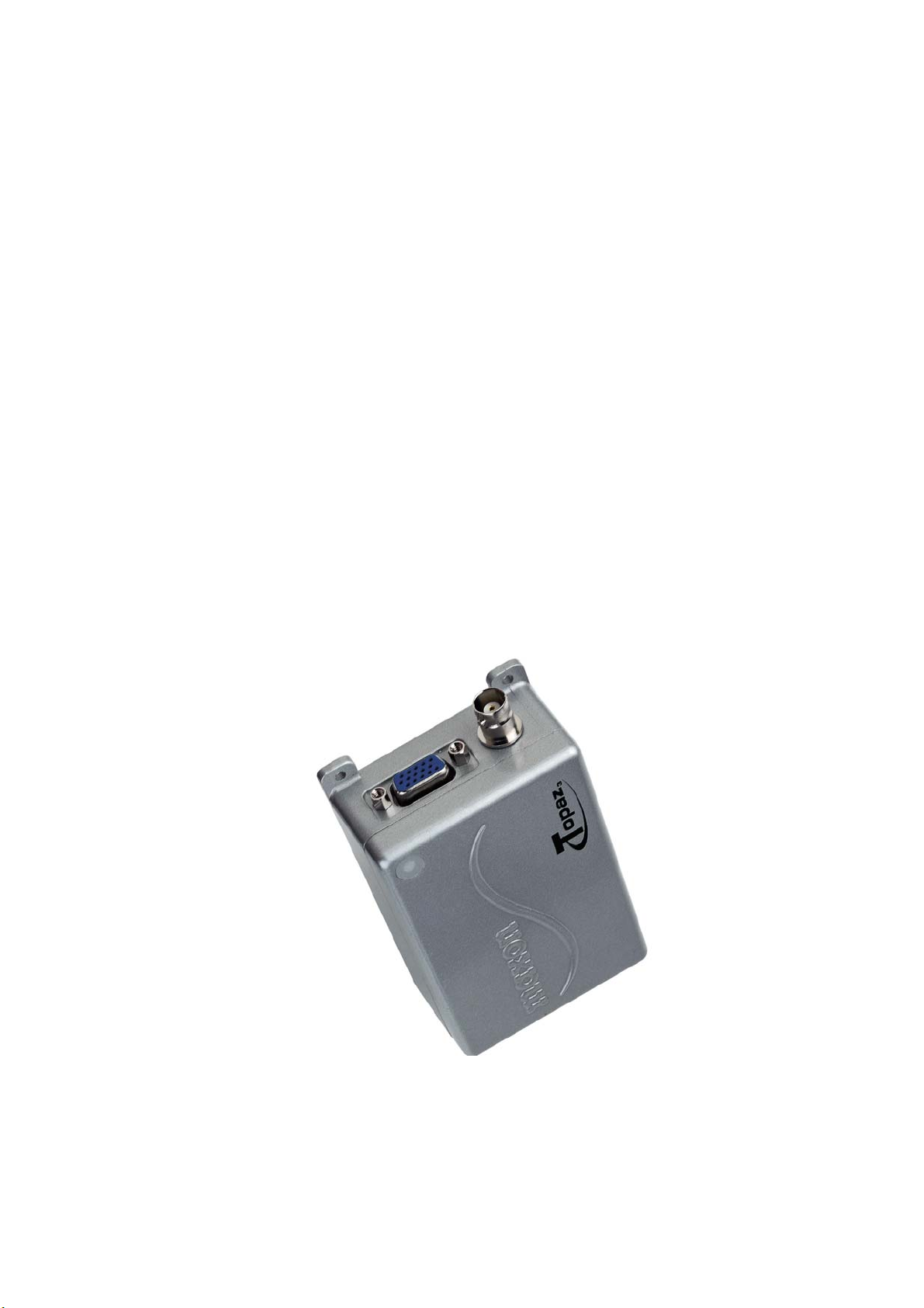
SD-160 Series Data Radio
(include SD-170 Series)
Technical Manual

TABLE OF CONTENTS
1. INTRODUCTION................................................................... 4
2. TECHNICAL SPECIFICATIONS ....................................... 5
3. FEATURES ............................................................................. 9
4. THEORY OF OPERATION ............................................... 23
4.1. INTRODUCTION ...........................................................................23
4.2. DIGITAL CIRCUITS ...................................................................... 23
4.3. RF CIRCUITS.................................................................................27
4.3.1. PLL SYNTHESIZER ................................................................................ 27
4.3.2. TRANSMITTER ....................................................................................... 28
4.3.3. RECEIVER .............................................................................................. 29
4.4. ACC-513 (GMSK MODEM CIRCUITS)........................................ 31
4.5. ACC-514 (FFSK MODEM CIRCUITS) ......................................... 32
4.6. ACC-515 (GPS INTERFACE CIRCUITS) ..................................... 33
5. MAINTENANCE AND REPAIR ........................................ 34
6. COMPONENT REPLACEMENT ...................................... 38
7. ALIGNMENT PROCEDURE ............................................. 40
7.1. RECEIVER...................................................................................... 41
7.2. TRANSMITTER ..............................................................................42
7.3. SQUELCH ADJUSTMENT ............................................................ 43
7.4. TEST EQUIPMENT SETUP ..........................................................45
2

8. INTERFACING .................................................................... 47
8.1. External connections ...................................................................... 47
8.2. DB-15 PIN descriptions with input/output level ............................ 47
8.3. Internal components ....................................................................... 49
8.4. Option board pin-out chart ............................................................50
8.4.1. ACC-513 (GMSK Modem Option board)................................................ 50
8.4.2. ACC-514 (FFSK Modem Option board)................................................. 50
8.4.3. ACC-515 (GPS Option board) ................................................................ 51
8.5. Wiring Diagram.............................................................................. 52
9. TROUBLE SHOOTING GUIDE ........................................ 53
10. VOLTAGE CHART ........................................................... 60
11. ELECTRICAL PARTS LIST............................................ 65
11.1. PARTS LIST FOR SD-161 ............................................................ 65
11.2. PARTS LIST FOR SD-164 ............................................................ 72
12. COMPONENT PINOUT.................................................... 79
13. SCHEMATIC DIAGRAMS............................................... 83
14. CIRCUIT B’D DETAILS................................................... 93
3

1. INTRODUCTION
The SD-160 and SD-170 Series (hereinafter called “the radios”) of RF wireless
modems from MAXON utilize the latest technology in its design and manufacturing. Both
the UHF and VHF models are Phase Lock Loop Synthesizer (PLL) / microprocessor
controlled and offer two watts (SD-160 Series) or one to five watts (SD-170 Series) of
power with 16-channel capability. Multiple functions including 1200 to 9600 baud rates,
AC and/or DC audio coupling, GMSK, FFSK and FSK modulation are standard in these
fully programmable wide bandwidth RF wireless modem units. Programmable sub-audio
squelch system (CTCSS & DCS) and two-tone squelch system are newly added to the
signal level detect squelch system (RSSI). GPS Data handling is provided to interface
and control internal GPS receiver.
The radios are programmed using an IBM
based software, an interface module and a programming cable. This allows the radio to
be tailored to meet the requirements of the individual user and of the System(s) it is
®
Personal Computer, DOS® or WINDOWS®
operating within.
4

2. TECHNICAL SPECIFICATIONS
GENERAL
Equipment Type : Data radio (Wireless Modem) Data radio (Wireless Modem)
Model Series : SD-161 SD-171 SD-164 SD-174
Performance Specifications : TIA/EIA-603 ETS 300-113 TIA/EIA-603 ETS 300-113
Frequency Range : 148-174MHz 148-174MHz 450-490MHz 450-490MHz
RF Output : 2W Only 1-5W 2W Only 1-5W
Channel Spacing : 12.5KHz, 25KHz Programmable
Modulation Type : F3D, F3E
Intermediate Frequency : 45.1MHz & 455KHz
Number of Channels : 16
Frequency Source : Synthesizer
Operation Rating : Intermittent
VHF UHF
90 : 5 : 5 (Standby : RX : TX)
Power Supply : Ext. Power Supply (12 VDC Nominal)
Temperature Range :
Storage
Operating
Current Consumption :
Standby(Muted)
Transmit 5Watts RF Power
Transmit 2Watts RF Power
Lock Time : < 10ms
TX to RX attack time : < 20ms (No Power Saving)
RX to TX attack time : < 20ms
Dimensions : (32mm)H X (58mm)W X (125mm)D
Weight : 253 grams
From -40°C to +80°C
From -30°C to +60°C
< 65mA
< 2.0 A
< 1.0 A
5
TRANSMITTER
Model Series : SD-161 SD-171 SD-164 SD-174
VHF UHF
Carrier Power : (Nom. Max. Min.)
Hi Power
Low Power
Sustained Transmission :
Time : 5 10 30Sec
(Nominal Conditions)
Frequency Error :
Nominal condition
Extreme condition
Frequency Deviation :
25 KHz Channel Spacing
12.5 KHz Channel Spacing
Audio Frequency Response : Within +1/-3dB of 6dB octave
Adjacent Channel Power :
2W < 3W > 1.5W
5W < 6W > 4.5W
N/A
Power : >90% >85% >80%
1W<1.5W>0.8W
< 0.5 KHz
±5.0 ppm
@ 300 Hz to 2.55 kHz for 12.5 kHz C.S.
@ 300 Hz to 3.0 kHz for 25 kHz C.S.
2W < 3W > 1.5W
Power : >90% >85% >80%
Peak ±5.0, Min. ±3.8
Peak ±2.5, Min. ±1.9
N/A
5W < 6W > 4.5W
1W<1.5W>0.8W
< 0.75 KHz
±5.0 ppm
25 KHz Channel Spacing
12.5 KHz Channel Spacing
Conducted Spurious Emission : < -60 dBc < -30 dBm < -60 dBc < -30 dBm
Modulation Sensitivity : 100mV RMS @ 60% Peak Dev.
Hum & Noise :
25 KHz Channel Spacing
12.5 KHz Channel Spacing
Modulation Symmetry : < 10% Peak Dev @ 1KHz input for nominal dev. + 20dB
Load Stability :
Peak Deviation Range Adjustment
@ 1 KHz, Nom Dev + 20dB :
25 KHz Channel Spacing
12.5 KHz Channel Spacing
< 70 dBc @ Nominal Condition , < 65 dBc @ Extreme Condition
< 60 dBc @ Nominal Condition , < 55 dBc @ Extreme Condition
> 40 dB (without PSOPH)
> 40 dB (with PSOPH)
No osc at ≥ 10:1 VSWR all phase angles and suitable antenna
No destroy at ≥ 20:1 all phase angle
Min. 3.5, Max. 6.0
Min. 1.5, Max. 4.0
6
RECEIVER
Model Series : SD-161 SD-171 SD-164 SD-174
Sensitivity (@ 12dB SINAD) :
25 KHz Channel Spacing
12.5 KHz Channel Spacing
Sensitivity ( 1/100 Error Rate)
With ACC-513
With ACC-514
Amplitude Characteristic : > -3dB , < +3dB > -3dB , < +3dB
Adjacent Channel Selectivity :
25 KHz Channel Spacing(Nom.)
(Extreme Condition)
12.5 KHz Channel Spacing(Nom.)
(Extreme Condition)
Spurious Rejection(100KHz ~ 4GHz) > 60 dB > 70 dB > 60 dB > 70 dB
Image / Half IF Rejection : > 60 dB > 70 dB > 60 dB > 70 dB
Intermodulation Response Rejection
±25 kHz/ 50 kHz
±50 kHz/ 100 kHz
Conducted Spurious Emission :
9 KHz - 1 GHz
1 GHz – 4 GHz
RX Spurious Emissions (Radiated) :
9 KHz - 1 GHz
1 GHz – 4 GHz
AF Distortion :
Nominal condition
Extreme condition
RX Hum & Noise (only audio) :
25 KHz Channel Spacing
12.5 KHz Channel Spacing
Receiver Response Time : < 16 ms < 16 ms
Squelch (factory pre-set)
Open
Close
Squelch Attack Time :
RF Level at Threshold
RF Level at Threshold + 20dB
Squelch Decay Time : 5 ms Min., 20ms Max.
Antenna Socket Input Match > 10 dB Return Loss
Temperature Stability for
L.O. Frequency :
L.O. Frequency Aging Rate : ±2 ppm/ year
< 0.28uV
< 0.30uV
< -113dBm
< -110dBm
> 65 dB
> 55 dB
> 55 dB
> 45 dB
> 60 dB
> 60 dB
< 5%
< 10%
< 40 dB without PSOPH
VHF UHF
< -57 dBm
< -47 dBm
< -57 dBm
< -47 dBm
< 40 dB with PSOPH
1st < 5 ppm, 2nd < 15 ppm from -30° to + 60° C
< 0.28uV
< 0.30uV
< -113dBm
< -110dBm
> 70 dB
> 60 dB
> 60 dB
> 50 dB
> 70 dB
> 70 dB
< 3%
< 10%
-113dBm
-116dBm
< 20 ms (RSSI), < 40 ms (Analog)
< 10 ms (RSSI), < 30 ms (Analog)
< 0.28uV
< 0.30uV
< -113dBm
< -110dBm
> 65 dB
> 55 dB
> 55 dB
> 45 dB
> 60 dB
> 60 dB
< -57 dBm
< -47 dBm
< -57 dBm
< -47 dBm
< 5%
< 10%
< 40 dB without PSOPH
< 40 dB with PSOPH
< 0.28uV
< 0.30uV
< -113dBm
< -110dBm
> 70 dB
> 60 dB
> 60 dB
> 50 dB
> 70 dB
> 70 dB
< 3%
< 10%
7
REFERENCE CRYSTAL
Model Series : SD-161 SD-171 SD-164 SD-174
Frequency : 12.8MHz
Holder Type : HC-18
Temperature Characteristic : ±5.0 ppm from -30° C to +60° C
Aging Rate :
VHF UHF
< 2 ppm/ year in 1st year
< 1 ppm/ year thereafter
ENVIRONMENTAL
Model Series : SD-161 SD-171 SD-164 SD-174
Temperature (deg C)
Operating
Storage
ESD 20 KV
Vibration MIL STD 810 C Procedures I, II, V and IEC68 26
Due to continuing research and development the company reserves the right to
alter these specifications without prior notice.
(performance without degradation unless stated)
VHF UHF
-30° to +60° C Degradation Specified @ Extreme condition
-40° to +80° C
8

3. FEATURES
16 Channels
The SD-160 Series(include SD-170 Series, hereinafter called “SD-160”) radio can store up to 16
channels within the same band. These channels can be selected by inner DIP-S/W or serial
command inputted from external control system.
Channel Spacing
The SD-160 is capable of programmable channel spacing, in both UHF and VHF bands. Each
channel can be programmed via the PC programmer, ACC-916, having 12.5KHz or 25KHz
channel spacing.
Output Power
In case of SD-160, 2-Watts output power is only available, but, in SD-170, it’s programmable.
Each channel can be programmed via the PC programmer to a high-power output, 5 Watts, and
a low-power output, 1 Watt.
Channel Scan
For audio application, SD-160 supports channel scan enabled via serial commands. During
programming of the radio, any channel can be selected as a scanned channel. When a scanned
channel is selected, it becomes a part of the scan list. Once the scan list has been established,
initiates scan by serial commands. If a conversation is detected on any of the channels in the
scan list, the radio will stop on that channel and audio signal will be released through pin 9 of
the DB-15 connector. At that moment, busy channel data is sent to external equipment or
device through serial command. So, busy channel data can be identified as decoding received
serial command from radio in the external equipment or device. Normally, if user tries to transmit
during scanning, the transmission will be made on the channel that the call is received during
the programmable scan delay time. (The scan delay time is the amount of time the radio will
stay on that channel once working has ceased. Dealer programming of 4 ~ 7 seconds is typical).
The radio will resume scanning once the scan delay time has passed, and will continue to scan
until the serial command for scan stop is inputted by external equipment. After the scan has
resumed, if a transmission is made, the radio will transmit on the selected priority channel. This
feature is similar to priority scan TX except for selection of priority channel. You can assign a
priority channel by inner dip switch only.
9

Scan Delete
To temporarily delete a channel from the scan list, simply input the serial command for scan
deletion to the radio while scanning and stopped on the channel to be deleted. This will
temporarily remove that channel from the scan list until the scan is closed or the radio’s power is
reset.
CTCSS / DCS Scanning
To help to block out unwanted calls to your radio, the SD-160 series can be programmed by
your dealer to scan for tones.
Busy Channel Lockout
This feature, when enabled, disables the transmitter when the user would attempt to transmit
during the receiving channel is busy. It will be dealer-programmable on/off and applicable to all
channels.
Marked Idle
When used in conjunction with Busy Channel, lockouted transmitter is allowed to operate as
long as valid RX tone is received. Dealers program this feature as ON or OFF. This feature will
be dealer-programmable on/off and applicable to all channels.
TX Time-out
This feature, when enabled, limits the amount of time that the user can continuously transmit.
This time can be set in increments by 10 seconds from 10 seconds to 990 seconds. If the user
attempts to transmit longer than the TX Time-out period, five seconds prior to expiration, the
radio will release Time-out alert signal through pin 9 of the DB-15 connector and will cease
transmission.
Power Save
The function of Power Save is used when an external battery is used as the power source.
When Power Save is enabled, the receiver ON and OFF time can be programmed and allows
the operator to set the length of time the receiver gets asleep.
Tx Delay
The TX will remain active for 150 ms at the end of TX when using CTCSS tones. This eliminates
squelch tail. Dealer programs this feature as ON or OFF.
10

Squelch Options
Compared to existing Maxon data radios, programmable sub-audio squelch system (CTCSS &
DCS) and two-tone squelch system are newly added. Each channel will have these squelch
option sets during dealer programming. More detail descriptions for all available squelch
systems of SD-160 are the following.
Sub-audio squelch system
The SD-160 can operate singly or with optional modem boards. Even if user wants to use sub-
audio SQ system, the radio will permit this SQ option according to some cases to avoid
confliction between sub-audio and data.
Contrary to general-purpose two-way radio, the input of the radio is data or audio. In case of
audio, its frequency spectra are limited to 300㎐ ∼ 3㎑ by internal BPF. So, the division of this
and sub-audio is possible on the frequency spectra because sub-audio has under 300㎐
frequency. But, Data has wide frequency spectra compared with audio. Normally, that has 30㎐
∼ 4.8㎑ frequency (except harmonic freq.) at 9600 baud rate. Accordingly, the conflict of sub-
audio and data are inevitable and so broken data or SQ error is unavoidable. To solve this
problem, the radios can use the FFSK modulation which converts data into two different
continuous audio tone according to their logic levels. Therefore, available cases of sub-audio
SQ system are Audio and FFSK signal. But, it’s not permitted to FSK(FM direct modulation of
data) and GMSK signal.
a.Single operation of SD-160
If the radio operates singly, only FM direct modulation/demodulation of audio and data are
available. In this case, audio and data are inputted and released through different DB
connector lines which pin 7, 9, 1 and 2 of DB-15 connector are used as audio input, audio
output, data input and data output, respectively. Normally, Sub-audio Squelch(SQ) System
can be applied to audio signal, but data doesn’t use it to avoid frequency confliction. So, if
user tries to transmit data in one channel which has sub-audio squelch option, radio will
flash green LED two times as warning and then transmit it without sub-audio.
Note : SD-160 provides the connection of external modems to receive and transmit
external modulated data which can be inputted and outputted through pin 1 and 2
11
of DB-15 connector, respectively. In this case, the external signals are referenced
to ground and may be a.c. or d.c. coupled depending on the user requirement.
Especially, if the type of external modem is AFSK or FFSK, Sub-audio
Squelch(SQ) System can be applied by dealer programming. For reference, its
related parameter is “Tx Tone Generation for Data Input” of “Tx option” group
on the “System Option / GPS” tap window of ACC-916.
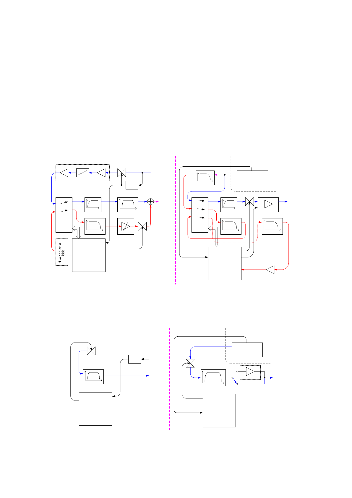
Brief block signal flow diagrams for each input are the following (See Figure 2.1. ~ 2.3.).
Audio Amp. & Filter
Z0
Z1
Y0
Y1
X0
X1
Analog S/W
MC14053B
Pre-emphasis
Z
Y
X
300Hz HPF
MF6
Sub-Audio LPF
Check Audio In
Tone En
High : Audio In
Low : No Audio
Data BPF
Adj. Level
Level
Detector
MCU
Sub-Audio
Encoder
Audio signal flow in Transmitter
Figure 3.1. Audio signal flow diagram
Audio In
Mod Out
RF Board
RSSI
AF
Busy
IF IC
TA31136FN
Audio Mute
LM386
Audio Amp.
4th Order
Sub-Audio LPF
MF6
Comparator
Audio Out
Pre-Selector
Z0
Z
Z1
Y0
Y
Y1
X0
X1
Analog S/W
MC14053B
300Hz HPF
X
MF6
Sub-Audio LPF
Audio Mute
RSSI
MCU
Tone Detector
Audio signal flow in Receiver
RF Board
RSSI
Data In
Level
Detector
High : Audio In
Low : No Audio
Data BPF
Check Audio In
Data Enable
MCU
If audio input is absent,
Data path will be enabled.
In this case,
Sub-audio option is ignored.
Data signal flow in Transmitter
Audio In
Mod Out
30Hz ~ 5KHz
BPF
Busy
MCU
RSSI
Data signal flow in Receiver
12
AF
IF IC
TA31136FN
Comparator
Data
Out
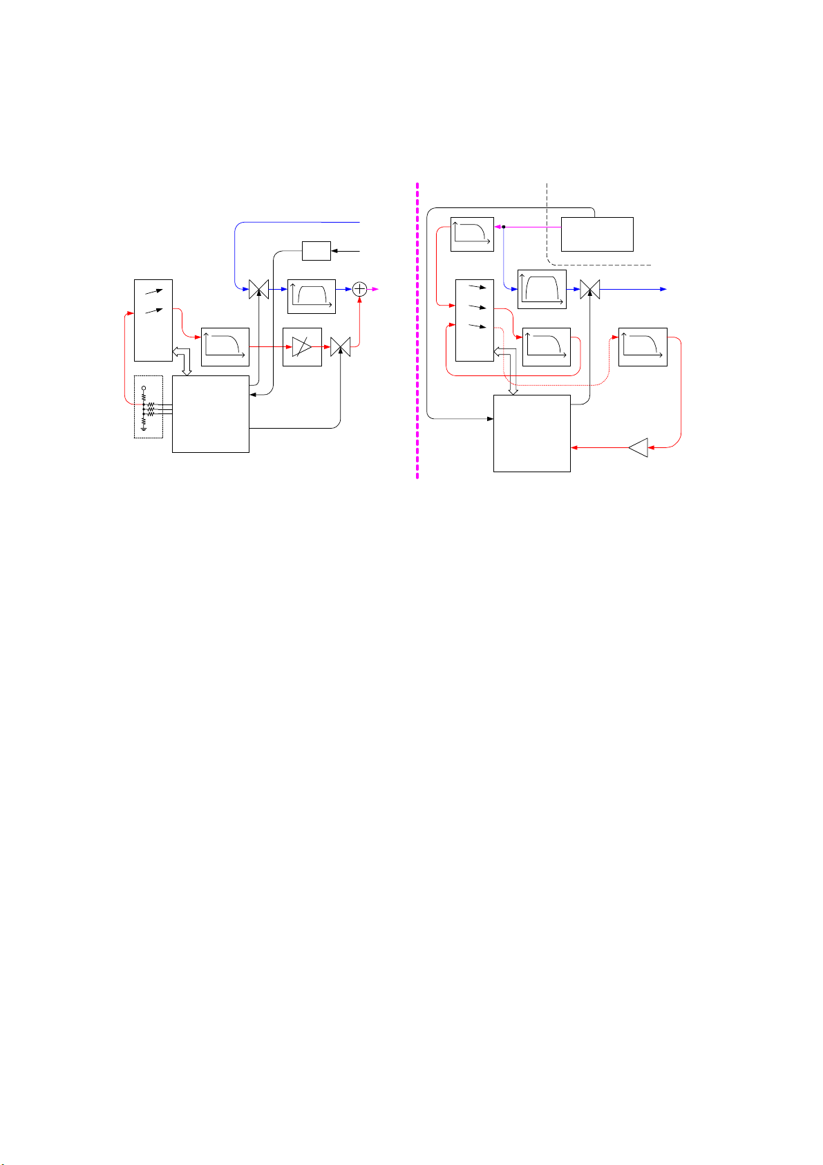
Figure 3.2. Data signal flow diagram
RF Board
Level
Detector
High : Audio In
Z0
Z1
Y0
Y1
X0
X1
Analog S/W
MC14053B
Z
Y
X
MF6
Sub-Audio LPF
Data Enable
Check Audio In
Low : No Audio
Data BPF
Adj. Level
MCU
Sub-Audio
Encoder
Tone En
Ext. Mod. signal flow in Transmitter
Figure 3.3. External modulated signal flow diagram
b. FFSK & GMSK
Data In
Audio In
Mod Out
RSSI
AF
Busy
IF IC
TA31136FN
4th Order
Sub-Audio LPF
Pre-Selector
Z0
Z1
Y0
Y1
X0
X1
Analog S/W
MC14053B
RSSI
30Hz ~
5KHz
BPF
MF6
Sub-Audio LPF
Z
Y
X
MCU
Tone Detector
MF6
Comparator
Ext. Mod. signal flow in Receiver
Audio Out
Maxon provides two optional modem boards, ACC-513, GMSK and ACC-514, FFSK for
SD-160 to improve the efficiency for data transmission and offer maximum flexibility for
user application. Selection of the required modulation option is made installing wanted
modem to radio and programming several modem parameters through PC-programmer,
ACC-916. Modem board provides the facility to connect a computerized controller via an
RS-232 level serial data interface (i.e. Communication port COM1, COM2, etc. for PCs) to
its Slave MCU. Received data from controller(DTE) will then drive the FFSK or GMSK
modulator and allow transmission of serial data. It also provides FFSK or GMSK
demodulator for the reception of FFSK or GMSK modulated data signals. These are
converted to RS-232 level serial data stream for supply to a computerized controller.
In application of Sub-audio squelch, it can’t apply to GMSK modulated signal because of
their frequency confliction. But, FFSK modulated signal can be mixed with sub-audio
because it consists of two different continuous tones which frequency spectra are on the
audio frequency region.
Brief block signal flow diagrams for each optional modem board are the following (See
Figure 2.4. and Figure 2.5.).
13
Z0
Z1
Y0
Y1
X0
X1
Analog S/W
MC14053B
RF Board
RSSI
AF
Pre-Selector
Z
Y
X
Sub-Audio LPF
Data BPF
MF6
Adj. Level
Tone En
Mod Out
Z0
Z1
Y0
Y1
X0
X1
Analog S/W
MC14053B
Z
Y
X
MF6
Sub-Audio LPF
IF IC
TA31136FN
4th Order
Sub-Audio LPF
Sub-Audio
Encoder
Master MCU
Rx_En
Tx_En
FFSK Modem
Option Board
Tx_Signal
(CMX469A)
Tx_CLK
Tx_Data_Out
Rx_CLK
Rx_Data_In
Slave MCU
Serial Data In Serial Data In
TxC
TDO
RxC
RDI
RSSI
Master MCU
FFSK Modem
Option Board
Rx_Signal
(CMX469A)
Busy
Rx_En
Tx_En
Tx_CLK
Tx_Data_Out
Rx_CLK
Rx_Data_In
FFSK signal flow in Transmitter FFSK signal flow in Receiver
Figure 3.4. FFSK signal flow diagram
RF Board
AF
Mod Out
Data BPF
TA31136FN
MF6Tone Detector
Comparator
Slave MCU
Serial Data Out
TxC
TDO
RxC
RDI
RSSI
IF IC
Serial Data Out
Sub-audio option is ignored.
Master MCU
Rx_En
Tx_En
Master MCU
RSSI
Busy
Rx_En
Tx_En
GMSK Modem
Option Board
Tx_Signal
(CMX589A)
Tx_Data_Out
Tx_CLK
Rx_CLK
Rx_Data_In
Slave MCU
TxC
Serial Data In Serial Data In
TDO
RxC
RDI
GMSK Modem
Option Board
Rx_Signal
(CMX589A)
Tx_CLK
Tx_Data_Out
Rx_CLK
Rx_Data_In
TxC
TDO
RxC
RDI
GMSK signal flow in Transmitter GMSK signal flow in Receiver
Figure 3.5. GMSK signal flow diagram
14
Slave MCU
Serial Data Out
Serial Data Out
c. CTCSS signal information
Each channel supports the 38 TIA/EIA standard tone frequencies and 11 non-standard
tones. All tones will be set up during dealer programming.
No. Freq.
(Hz)
01 67.0 11 97.4 21 136.5 31 192.8 41 171.3
02 71.9 12 100.0 22 141.3 32 203.5 42 177.3
03 74.4 13 103.5 23 146.2 33 210.7 43 183.5
04 77.0 14 107.2 24 151.4 34 218.1 44 189.9
05 79.7 15 110.9 25 156.7 35 225.7 45 196.6
06 82.5 16 114.8 26 162.2 36 233.6 46 199.5
07 85.4 17 118.8 27 167.9 37 241.8 47 206.5
08 88.5 18 123.0 28 173.8 38 250.3 48 229.1
09 91.5 19 127.3 29 179.9 39 69.3 49 254.1
10 94.8 20 131.8 30 186.2 40 159.8
d. DCS signal information
No. Freq.
(Hz)
No. Freq.
(Hz)
Table 3.1. CTCSS Frequency Chart
No. Freq.
(Hz)
No. Freq.
(Hz)
The radio supports the encoding and decoding of 104 DCS data (include TIA/EIA code).
Octal
Code
Octal
Code
Octal
Code
Octal
Code
Octal
Code
Octal
Code
Octal
Code
Octal
Code
Octal
Code
Octal
Code
Octal
Code
023 054 125 165 245 274 356 445 506 627 732
025 065 131 172 246 306 364 446 516 631 734
026 071 132 174 251 311 365 452 523 632 743
031 072 134 205 252 315 371 454 526 654 754
032 073 143 212 255 325 411 455 532 662
036 074 145 223 261 331 412 462 546 664
043 114 152 225 263 332 413 464 565 703
047 115 155 226 265 343 423 465 606 712
051 116 156 243 266 346 431 466 612 723
053 122 162 244 271 351 432 503 624 731
Table 3.2. DCS Code Chart
15

Two-Tone Squelch(SQ) System
The radios will support Motorola-Format, Two-Tone(Type 99) decoding. This is receive only,
decode only feature. It will allow a dispatcher to call individuals and groups. Each
System/Group will be programmable to respond to any combination of the code, with a
distinctive alert for each System/Group. The alert format consists of two tone sequences, first
the ID of the radio being called, then the ID of the calling radio.
This feature is programmed by the dealer(per customer’s request) and is not activated /
deactivated by the user. The user interface consists of the radio emitting the tones being
broadcast. At this point, the radio will enter Unmuted Rx mode and remain in this mode until the
PTT signal is inputted.
Serial command
To give the simplest protocol for control of radio, Maxon has prepared for some serial
commands which have an ease to encode and decode format. SD-160 can be used without
serial commands, but user can use its various functions through application of those, for
instance, setting-up the basic radio operation such as channel change, switch of RX/TX and
channel scan, moreover, used for control of GPS and modem option board. All messages are in
binary format, which reduces required data size to shorten response time of radio and follows
below data format.
Serial RX/TX Data Format
(1) Asynchronous Serial Data Transfer
(2) Baud Rate : 4,800 bit/sec
(3) Data Bit : 8bit , Non Parity
(4) Stop Bit : 1bit
(5) MSB first transmission
Each serial command is consist of 3 bytes. 1
command and 3
is check sum to decide validity of total contents.
rd
byte is command and 2nd is data required by
st
Byte0
ST 1
Byte (Command) SP
st
Byte1
ST 2
Byte (Data) SP
nd
Byte2
ST 3
rd
Byte (Check Sum) SP
16
Data Protocol
a. Protocol for input serial command
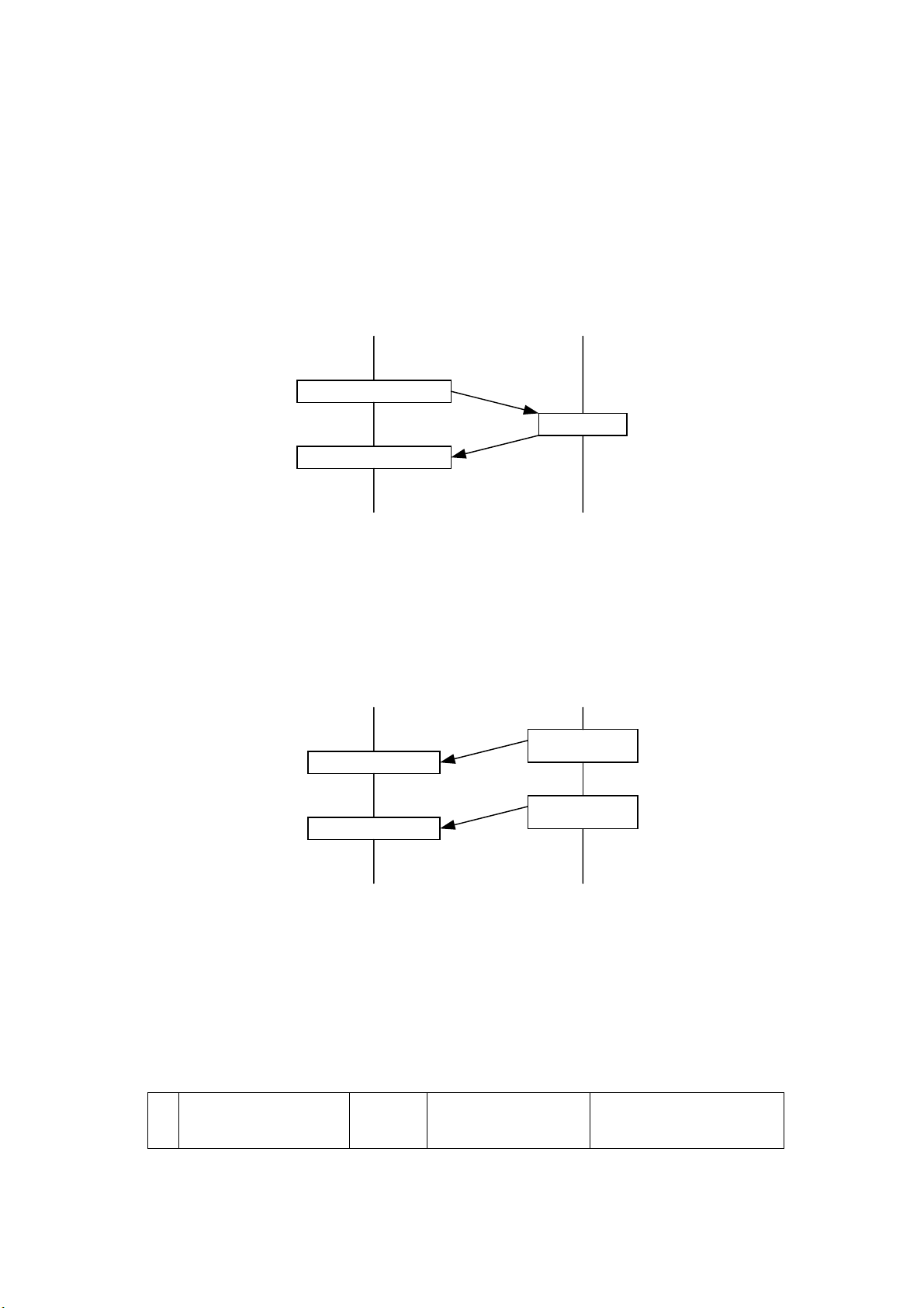
Protocol of data transmission from external equipment or device (: PC) to radio :
External equipment or device Radio
Input serial command
Response
Receive response
Figure 3.6. Protocol for input serial command
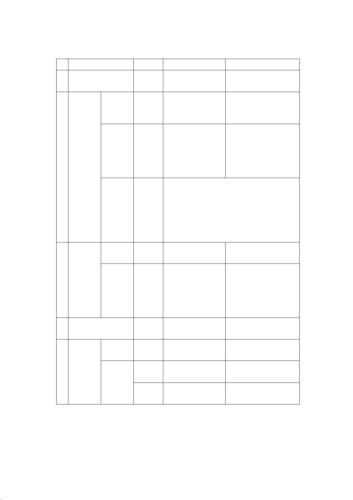
b. Protocol for output data
Protocol of data transmission from radio to external equipment or device (: PC) :
External equipment or device Radio
Output Data
Receive Data
(with command)
Output Data
Receive Data
(with command)
Figure 3.7. Protocol for output data
Detail information of Serial Commands
a. Transmitting Command & Data
Mode
Command
(BYTE0)
17
Data
( BYTE1 )
Check sum ( BYTE2 )
: Command + Data
1. Channel Change 0x64 0x?? :Current channel ( 0x64 + Channel )
2.
RTX Mode Selection
3.
Scan Mode
From PC
To Radio
From Radio
To Pc
Error
Message
0x61 R(0x72) : Rx mode
T(0x74) : TX mode
0x62 F(0x46) : Scan Stop
S(0x73) : Scan Start
O(0x4F) : Scan Delete
0x66 0x00 : 1 Channel
0x01 : 2 Channel
0x02 : 3 Channel
M
0x0f : 16 Channel
( 0x61+0x72 )
( 0x61+ 0x74 )
( 0x62+ 0x46 )
( 0x62+ 0x73 )
( 0x62+ 0x4F )
0x66 + 0x00
0x66 + 0x01
M
*Only for Unmute Channel,
Correct Call Channel
0x65 It occurs when Scan Delete command comes except
Busy/Correct Call
It occurs when PTT key is pushed except
Busy/Correct Call.
It occurs when channel change command exists
during Scanning.
4.
5.
Modem test mode
6.
Modem
alignment
GPS
mode
mode
Control of
GPS Power
0x6a 0x00 : GPS Power Off
0x01 : GPS Power On
0x63 0x00 : GPS Data Disable
0x01 : Release GPS Data
( 0x6a + 0x00 )
( 0x6a + 0x01 )
( 0x63 + 0x00 )
( 0x63 + 0x01 )
Control of
to DB-15
GPS Data
0x02 : Release GPS Data
( 0x63 + 0x02 )
to Modem
0x75 0x78 : Enable test data
0x79 : Disable test data
0x7a 0x00 : Disable
( 0x75 + 0x78 )
( 0x75 + 0x79 )
( 0x7a + 0x00 )
GMSK
0x01 : Enable
0x7c 0x00 : Disable
0x01 : Enable Mark data
( 0x7a + 0x01 )
( 0x7c + 0x00 )
( 0x7c + 0x01 )
FFSK
0x7e 0x00 : Disable
0x01 : Enable Space data
( 0x7e + 0x00 )
( 0x7e + 0x01 )
Table 3.3. Composition of input serial commands
18

Receiving Command & Data
Command
Data
Check sum (BYTE2)
Mode
(BYTE0)
(BYTE1)
: Command + Data
0xaa ACK N/A 1 Process Complete
Commands
0x55 NACK N/A
Table 3.4. Composition of response commands
Note)
This command is return signal for receiving command.
If Byte2 and sum of Byte0 and Byte1 among received data are same, Radio would
send ACK data and execute command. If not, Radio sends Nack data.
User would go into next step if receives ACK data. If receiving Nack data, user should
send command again.
example) If user changes from 1
st
Channel to 2nd Channel,
user should send Channel Change Command ( 0x64,0x02 , ( 0x64 + 0x2 ) ) to Radio.
If Byte2 and sum of Byte0 and Byte1 among received data are same, Radio sends
ACK data to user and goes to 2
nd
channel. If not, radio would send Nack data.
Status indicators and audible alert tones
SD-160 series data radio has a sophisticated microprocessor control which provides a range of
LED displays. LED displays operation mode, current status of radio, warning, and etc. Moreover,
if you connect the Speaker filtered OUT (Pin 9 of DB-15 connector) to an external speaker, you
can hear audible tones under the following conditions:
• Attempt to transmit on a channel which is already in use when busy channel lockout option
has been programmed
• Transmission time has exceeded time-out timer programmed length
• The other group or people has finished transmission using repeater
See the status indicators and audible alert tones chart (Table 2.5.) for full specification.
19
STATUS DESCRIPTION LED COLOR AUDIBLE TONE
POWER ON -
Busy Channel Yellow
NORMAL
SCANNING
WARNING
Correct Call Green
Transmit Yellow
Transmit Not Allowed
Normal Scan Mode Green LED Flash
Scan Delete one time Red LED
Scan All Delete Two times Red LED
Busy Channel lockout two times Green LED Single Beep Tone
Time out Time one time Green LED
Before 5S T-O-T one time Green LED Single Beep Tone
EEPROM Error one time Yellow LED
Unlock Four times Yellow LED
Communication error with Modem
Green LED flash
MCU
Transmit Hang on time - Single Beep Tone
Under channel programmed sub-
Two times Green LED
audio SQ, when transmission is
tried by input of FSK or GMSK
data.
Read Mode Red LED flash
PROGRAM
Write Mode Green LED flash
AUTO TEST Yellow
Open Squelch Mode three times Green LED
SQUELCH
PROGRAM MODE
Close Squelch Mode Two times Green LED
Save Squelch Mode One time Green LED
Init Data Load one time Green LED
Table 3.5. status indicators and audible alert tones
20

Modem Option for data communication
ACC-513 and ACC-514 are new kinds of internal option-modems, which are applied to SD-160
series to increase capability for data application. The goal of internal modem is to improve the
efficiency for data transmission and provide maximum flexibility for user application. In former
case, the most obvious method of increasing the efficiency is to maximize the data signaling
speed in the limited channel bandwidth. But, FSK, called direct FM modulation, has very wide
transmission bandwidth requirement. To solve this problem, Maxon supplies GMSK(Gaussian
Filtered Minimum Shift Keying) internal option-board. In latter case, to improve quality of service,
some of service provider (or user) want to apply new radio to their existing system without
additional investment to establish new system even if it’s audio system. But, data application
can’t be directly applied in audio system because of its spectra characteristic. Generally, spectra
of data have wider bandwidth than audio. So, direct application of data is not matched with
audio system and its application. For instance, if sub-audio(Tone) SQ system is applied to data
application, its frequency spectra conflict with that of sub-audio. Moreover, if inputted data is
filtered by audio filter circuit to avoid this problem, some of that will be broken. Therefore, to get
over these problems and provide maximum flexibility, Maxon prepares FFSK(Fast Frequency
Shift Keying) internal option-board.
Our internal modem option boards consist of Slave MCU, Modem IC, and extra circuitry. These
option-boards directly communicate with DTE (Data Terminal Equipment) to send and receive
the meaningful data through the DB-15 connector on digital board of SD-160. These are
designed to accept RS232 serial data format and also capable of high speed wireless data-
transmission between two or more devices. More detail information for modem option boards is
given in technical manual for ACC-513/514. Moreover, dealer will help you define a TX On/Off
Delay time, RX On Delay time, Baud Rate, Modem Enabled, Modem Baud Rate, Data flow
control, and Test Mode.
Table for modem speed
Channel Space DTE Baud Rate Modem Baud Rate
Narrow (12.5KHz)
Standard (25KHz)
1200 1200
2400 2400
1200 1200
2400 2400
4800 4800
Table 3.6. Available Baud rate for FFSK modem
21

Channel Space DTE Baud Rate Modem Baud Rate
Narrow (12.5KHz)
Standard (25KHz)
Table 3.7. Available Baud rate for GMSK modem
4800 4800
4800 4800
9600 9600
GPS option board
As one of methods to satisfy various requests for user application, SD-160 basically supports
GPS data handling. That may help your implementation for system related to GPS.
Nevertheless, if it’s not enough for each your application, received position data from GPS
module placed in SD-160 can be reprocessed by your own application. ACC-515 is GPS
module for SD-160, which releases some of 11 different output data according to NMEA-0183
format. Moreover, it can be also selected by user, but it should be processed by user’s
application. Received data from ACC-515 will be released via DB-15 connector of SD-160
or/and transmitted to other system through installed modem. More detailed information for GPS
option board is given in technical manual for ACC-515.
22

4. THEORY OF OPERATION
4.1. INTRODUCTION
The VHF and UHF radios comprise of two PCBs (RF and digital PCB). These boards are
connected by an 18 pin female and male connector. The digital board which controls the radio
and data receiving and sending is interfaced with external data equipment through the 15 pin d-
sub female (DB-15) connector.
4.2. DIGITAL CIRCUITS
The Digital circuit contains the CPU, the channel select switch, and associated digital circuits.
TX-SIGNAL CIRCUIT
There are two signal paths in the Tx-signal circuit. One is FSK data signal path and the other is
the audio signal path. The FSK data signal from Pin 1 of DB-15 connector (CON401) goes
through IC406-C. The signal is amplified by IC404-C and then its amplitude is limited by IC404-
D. After that, this signal is filtered by an 8’th order low pass filter (IC405) in order to reduce the
required transmission bandwidth. The first two stages of the 8’th order LPF consist of a
Gaussian filter for the improvement of ramp function response and the last two stages use a
Butterworth filter for attenuation. The output of the LPF is then fed to the RF board for TX
modulation.
Audio signal, from Pin 7 of DB-15 connector is fed into the 300Hz High pass filter(IC408)
through the IC406-B and IC409. The HPF removes sub-audible voice products for application of
Sub-audio(Tone) squelch system (CTCSS, DCS) and then the output from IC408 is fed into
IC404-A&B with associated parts to form a mic amplifier and pre-emphasis circuit. After that, the
pre-emphasized Tx-audio signal is inputted to the RF board for Tx modulation through the FSK
data signal path.
RX-SIGNAL CIRCUIT
The Rx-signal circuit also has two signal paths. One is the data signal path and the other is the
audio signal path. The Rx signal comes from the RF board, which is connected with pin 10 of
CON405. Data signals are switched in IC406-D by a Busy signal which is activated when the
radio receives a valid RF signal, and is filtered by IC416-A and then its amplitude level is
23

adjusted (amplified) by IC416-B. The amplitude-adjusted signal goes to pin 2 of the DB-15
connector (CON401).
Audio signals are inputted to the 300Hz High pass filter (IC408) to eliminate sub-audible voice
products through IC409. The output of the HPF is switched by IC406-A and de-emphasized by
resister R471 and C452. After that, its level is adjusted by RV401 and then that is amplified by
IC412 (LM386 : Audio amplifier). The amplified signal goes to pin 9 of CON401 (DB-15).
ANALOG SWITCH
IC409 (MC14053B) is a digitally controlled analog switch which internally consists of three
single pole, double throw switches. By placing a high (5V) or low (0V) on the control lines which
consists of A, B and C. A controls the X ports, B controls the Y ports and C controls the Z ports.
Example: A high on control A would connect X to X1. A low on control A would connect X to X0.
HIGH PASS FILTER
The 300Hz high pass filter is an 8-pole 1dB Chebeyshev active filter that comprises of IC410
and associated components. Received audio is passed to IC408 from Pin 4 of IC409 where
sub-audible tones below 300Hz are removed. Tx (Mic) audio is also fed into IC408 via IC 409
(Pin 4) where sub-audible voice products below 300Hz are also removed.
CTCSS/DCS DECODE CIRCUITS
Discriminated audio from Pin 9 of IC6 is fed into IC411-B and associated parts which are the
first 2 poles are part of a 6th order 250 Hz Chebeyshev low pass filter. The output from pin 1
(IC411-B) is fed into IC409 (Pin 2) and outputs to pin 15 (IC409). The signal is then fed to Pin 8
(IC410) which is a 6th order low pass Butterworth switched capacitor filter. The output from the
Butterworth filter (Pin 3 of IC410) is then fed to the remaining second 4 poles part of the 6th
order Chebeyshev filter, which consist of IC411-D and one of the two internal operational
amplifiers of IC410 (MSNBLPS) along with associated components. Both the Chebeyshev and
the Butterworth combines for a 4dB ripple low pass filter when programmed for 250 Hz. The
output of IC411-D (Pin 14) is fed into the remaining internal operational amplifier of IC410
(MSNBLPS) which forms the squaring circuit for the signal decode. The signal is out from Pin 2
of IC411 (MSNBLPS) and fed into IC401 (MCU) where it is compared whether that is matched
with preprogrammed data or not. If matched, valid data is decoded, shown by a green L.E.D.
on the top panel of the radio, and audio is released through pin 9 of DB-15 Connector. If
24

unmatched, the busy L.E.D. (Yellow) would be shown.
CTCSS/DCS ENCODE CIRCUITS
During TX encode, the tone squelch digital signal is produced as a 3-bit parallel word at Pins 33,
34, and 35 of the micro controller (IC401). The 3-bit digital signal is converted to an analog
signal by resistors R481, 482 and 483. The analog signal is fed into Pin 1of IC409 and out on
Pin 15 (IC409) and then fed into Pin 8 of IC410 (6th order Butterworth clock tuned low pass
filter). The filtered encode output from Pin 3 (IC410) is fed to IC411-A and RV402 (sub-audible
gain control), the output of IC411-A is then fed to the audio mixer circuit of the RF board.
TWO TONE DECODE CIRCUITS
Two tone uses frequency with audio. Discriminated audio from the RF board is inputted to the
comparator (two tone decoder : IC403-B) which forms the squaring circuit for the decode signal.
The signal is output from Pin 7 of IC403-B and fed into IC401 (MCU) where it is compared
whether it is matched with preprogrammed data or not. If matched valid data is decoded, which
is shown by a green L.E.D. on the top panel of the radio and audio is released through pin 9 of
the DB-15 Connector. If unmatched, the busy L.E.D. (Yellow) is shown.
RSSI DETECTOR
From the RF board, the RSSI (Received Signal Strength Indicator) signal flows to Pin 31 of
IC401(MCU) through R513. Micro controller unit (IC401) detects received signal level using the
inner 8-bit ADC(Analog to Digital Converter). The output of ADC is compared with the
programmed RSSI level. If the MCU detects existence of a received signal through these
comparison a yellow L.E.D. is shown on the top panel of the radio.
EEPROM
RX / TX channel and RSSI detection level as well as other data from the programmer are stored
in the EEPROM. The stored data is retained without power supply. This is a non-volatile
memory and re-programmable. IC402 is an EEPROM with 4096 (8 x 512) capacity and data is
written and read serially.
25

CHANNEL SELECTOR
One of 16 channels may be selected using the Dip Switch (SW401) and serial commands. The
hardware selector, SW401 encodes the channel number, selected into 4-bit binary code. The
binary code plus one equals the channel number. The binary code is decoded by the CPU,
which enables the appropriate RX or TX frequency and associated data to be selected from the
EEPROM. External serial commands which come from Pin 8 of the DB-15 Connector (CON401)
are fed into Pin 41 of IC401 (MCU). The micro controller uses UART (Universal asynchronous
receiver transceiver) for serial communication and decodes serial commands in order to control
the radio.
DC TO DC CONVERTER
The main DC power is supplied to the switched mode DC to DC converter . The DC to DC
converter regulates the various input power supply voltage and outputs a constant voltage of
6.5 Volts (SD-161, SD-164) or 7.5 Volts (SD-171, SD-174). It is a source for all of the RF and
digital circuits. The DC to DC converter is formed by IC801, Q801, Q802, L801, R804 and
voltage divider(R805, R806, R802). IC801 is a PWM controller that controls pulse width of the
switching pulse output. Various input voltage appears as various output voltage of voltage
divider. IC801 detects the voltage difference between inner reference voltage and the voltage
divider output controls the switching pulse width in proportion to its difference. Wanted output
voltage is decided by product of input voltage and duty ratio of switching pulse. As the switching
pulses, Q801and Q802 switch the input DC of various supply voltages and generate the
constant DC of supply voltage. IC801 controls maximum current of DC to DC converter by
current detection through voltage drop of R804.
26

4.3. RF CIRCUITS
4.3.1. PLL SYNTHESIZER
12.8 MHz TCXO
The TCXO contains the 3-stage thermistor network compensation and crystal oscillator and
modulation ports. Its compensation is ±5 PPM or less from -30c to +60c.
PLL IC DUAL MODULE PRESCALER
Input frequency of 12.8 MHz to pin 1 of IC2 MB15A02 (or MB15E03SL) is divided into 6.25 kHz
or 5 kHz by the reference counter and then supplied to the comparator. RF signal input from the
VCO is divided to 1/64 at the 64/65 modulus prescaler in IC2, divided by A and N counter in IC2
to determine frequency steps, and then supplied to the comparator. PLL comparison frequency
is 6.25/5 kHz, so its minimum programmable frequency step is 6.25/5 kHz. The A and N counter
is programmed to obtain the desired frequency by serial data in the CPU. In the comparator, the
phase difference between reference and VCO signal is compared. When the phase of the
reference frequency is leading, ΦP is the output, but when the VCO frequency is leading, ΦR is
the output. When ΦP= ΦR, phase detector out is a very small pulse.
EXTERNAL CHARGE PUMP
This is used to increase dynamic range of VCO. Voltage range is decided by the supply voltage
of the charge pump and the DC to DC converter which supplies that voltage. 0-12v is necessary
for controlling the VCO. In addition the radio adopts a current mode charge pump to take direct
control of such parameters as charge pump voltage swing, current magnitude, TRI-STATE
leakage, and temperature compensation. ΦP, ΦR logic signals are converted into current
pulses to enable either charging or discharging of the loop filter components to control the
output frequency of the PLL.
REFERENCE FREQUENCY LPF
The Loop Filter contains R9, C1 and C2. LPF settling time is 12mS with 1 kHz frequency. This
also reduces the residual side-band noise for the best signal-to-noise ratio.
27

DC TO DC CONVERTER
The DC to DC converter converts 5v to 14-16v to supply the necessary voltage for wide range
frequency in the VCO.
VCO
The radio adopts a two VCO system for RX and TX in order to maximize each performance.
The TX and RX VCO generates RF carrier and local frequency and each VCO is switched by a
TX/RX power source. It is configured as a Colpitts oscillator and connected to the buffer as a
cascade, the bias circuit is a cascade configuration to save power. The varicap diode
D201/D301are low-resistance elements and have different capacitance for reverse bias voltage.
Using the change of reverse bias voltage (2 ~ 11V), the wanted frequency for each channel can
be obtained. L203/L303 are resonant coils and C208/C308 are used to change the control
voltage by the tuning core. D202 modulation diode modulates the audio signal. C204
compensates the non-linearity of the VCO due to the modulation diode and maintains a
constant modulation regardless of frequency.
4.3.2. TRANSMITTER
The transmitter consists of:
1. Buffer
2. P.A. Module
3. Low Pass Filter
4. Antenna Switch
5. A.C.C. Circuits
BUFFER
VCO output level is -4dBm and amplified to +10dBm. The buffer consists of Q9 and Q10 for
reverse isolation and gain.
P.A. BLOCK
The P.A. Block uses a three stage amplifier and contains Q501, Q502, and Q503. The SD-171,
SD-174 have different amplifiers applied compared to the SD-161, SD-164 because different of
a output power specification. Q501 amplifies the TX signal from +10 dBm to 100mW and Q502
28

amplifies to 0.5W and Q503 amplifies to 3W(SD-161, SD-164) or 6W(SD-171, SD-174) and
then matched to 50 Ohms using the L.C. network or strip line, thereby reducing the harmonics
by -30 dB.
LOW PASS FILTER
L7, L8, L9, C36, C37, C38 and C39 are the 7th order Chebyshev low pass filter. Unwanted
harmonics are reduced by -70 dBc.
ANTENNA SWITCH
When transmitting, the diodes D3 and D5 are forward biased to enable to make an RF path to
the antenna. D5 is shorted to ground to block the RF signal to the front-end. In receive, the
diodes, D3 and D5, are reverse biased to pass the signal from the antenna through L10 and
C61 to the front-end without signal loss.
AUTOMATIC CURRENT CONTROL (ACC) CIRCUITS
The ACC circuit consists of R63, variable resistor RV4, IC5(B) and transistors Q11 and Q12.
The supplied current to the P.A. block is monitored by the voltage difference on R63 (0.1 Ohm).
If the current varies by RF power output or other reasons, it produces a voltage difference on
R63 and then IC5A outputs a bias voltage to Q19 in proportion to that difference. The adjusted
value of Q15 output by RV4 is compared with the reference voltage in IC5B and then a
differential voltage at the output of IC5B is passed to Q12 and Q11 which controls the bias
voltage of the P.A. module to maintain a constant power output to the antenna. RV4 is used to
adjust the RF power level.
4.3.3. RECEIVER
FRONT-END
The front-end block consist of two band pass filters and a low noise amplifier (LNA). The Band
pass filter is used for elimination of image frequency and impedance matching and the LNA is
used to amplify weak RF signals without any increase of noise. The received signal comes from
the antenna, then is input into a band pass filter of the front-end block with C601through C610,
L601 through L604 at UHF and C622 through C608, L607 through L604 at VHF, and is coupled
29

to the base of Q601 serving as an RF amplifier. Diode D601 serves as protection from static RF
overload from nearby transmitters. The output of Q601 is then coupled to a second band pass
filter consisting of C611 through C623 and L606 through L609 at UHF and C607 through C601,
L603 through L601 at VHF. The output of the front-end block is then coupled to the double
balanced diode mixer D6. The Front-end block is pre-tuned at factory and no more adjustment
is required
FIRST MIXER
The Double balanced diode mixer consists of D9, T1 and T2 and generates the 45.1 MHz
intermediate frequency output from RF and local frequency. The filtered frequency from the
front-end module is coupled to T1and the local frequency from RX VCO is coupled to T2. The
45.1 MHz IF output is matched with the input of the 2-pole monolithic filter by L12, L13, C65 and
C66. The crystal filter provides a bandwidth of ±7.5 kHz at the operating frequency for a high
degree of spurious and inter-modulation protection. The IF filter provides additional attenuation
for the image frequency of the second mixer. The output impedance of the filter is matched with
the base of the post amplifier Q16 by C67 and C70.
SECOND OSCILLATOR MIXER LIMITER AND FM DETECTOR
The output of the post amplifier, Q16, is coupled via C71 to the input of IC6 (TA31136FN). IC6
is a monolithic single conversion FM transceiver, containing a mixer, the second local oscillator,
limiter and quadrature detector. Crystal X1, 44.645 MHz, is used to provide resultant 455kHz
signal from the output of the second mixer. The mixer output is then routed to CF1 (455F) or
CF2(455HT). These ceramic filters provide the adjacent channel selectivity of 25 kHz or 12.5
kHz bandwidth. After that, filtered signal is fed to the limiter and then audio is derived from the
limited signal at the quadrature detector.
RSSI ( RECEIVER SIGNAL STRENGTH INDICATOR )
The RSSI signal is output from IC6 on pin 12. The output is an analog DC voltage and varied as
much as the received signal strength. The signal which is filtered unwanted noise by the low
pass filter (IC4-B) in the RSSI signal is used for squelch system. Also, this signal is
compensated with a thermistor (TH3) at temperature.
30
 Loading...