

Page 1
XR31233 / XR31234 / XR31235
Evaluation Board User’s Manual
Introduction
Exar’s XR31233 / XR31234 / XR31235 EVB evaluation
board provides a platform on which to examine the features
and performance of the XR31233 / XR31234 / XR31235
CAN Bus transceivers. The XR31233 / XR31234 / XR31235
EVB is a 2 layer pcb that allows for access to all the device
pins.
Hardware Setup
To use the Evaluation Board, the following components are
required:
1. XR31233 / XR31234 / XR31235 EVB evaluation board
2. Power supply
3. Signal source
4. Oscilloscope for data analysis
5. Digital Multimeter
Refer to the product data sheet for additional information.
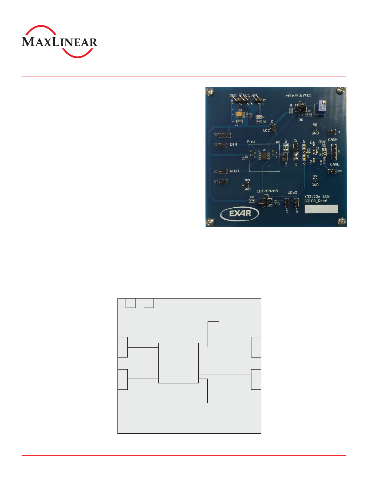
Figure 1:
Top View of XR31233 / XR31234 / XR31235 EVB
Evaluation Board Overview
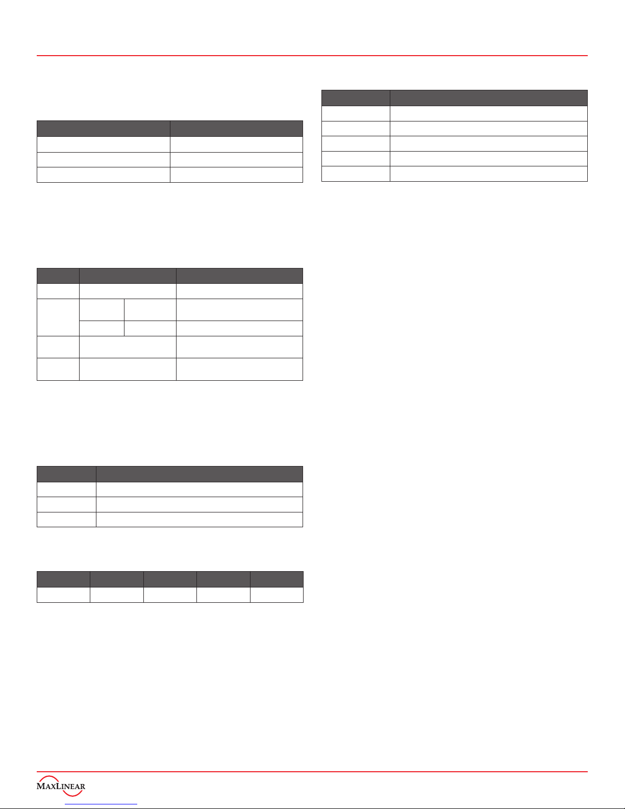
The block diagram shown in Figure 2, illustrates the connection points for the CAN Bus, power and ground, TTL/CMOS
driver input, TTL/CMOS receiver output and the mode pins.
TTL/CMOS
Driver Input
TTL/CMOS
Receiver Output
GND
DIN ROUT
PWR
DUT
RS Mode Selection
CAN Bus
CANL CANH
LBK/EN/AB Selection
Figure 2: Block Diagram XR31233 / XR31234 / XR31235 - EVB
1/8
Page 2
XR31233 / XR31234 / XR31235 Evaluation Board User’s Manual
Hardware / System Setup
The EVB is factory installed with the CAN Bus transceiver
per Table 1.
CAN Bus Transceiver Evaluation Board
XR31233 XR31233EDEVB
XR31234 XR31234EDEVB
XR31235 XR31235EDEVB
Header Probe Point
J3 VCC into transceiver
J6 Driver input from CAN Controller to pin 1 (D)
J9 Differential CANH and CANL probe
J12 Receiver output from pin 4 (R) to CAN Controller
J14 VRxD (see next section).
Table 1: Evaluation Board Part Numbers
Jumpers are factory installed per Table 2 to configure
the EVB for normal mode operation. Jumper and testing
options are described in the next section.
Header Factory Setting Description
E1 Jumper 1-5 RS = GND, high speed mode
XR31233
E2
J7 Jumper 1-2
J10 Jumper 1-2
XR31235
XR31234 Jumper 3-5 EN = 1 enables normal mode
Jumper 4-5
LBK = 0 enables normal mode
AB = 0 enables normal mode
Connects 120Ω between
CANH and CANL
Connects 120Ω between
CANH and CANL
Table 2: Factory Settings
Connect the CAN Bus, TTL/CMOS Driver Input and
Receiver Output per Table 3 and power and ground per
Table 4 for immediate operation.
Header Connection
J5-2 TTL/CMOS Driver Input from CAN Controller
J8 CAN Bus
J11 TTL/CMOS Receiver Output to CAN Controller
Table 3: Input and Output Connections
Table 5: Monitoring Probes
Jumper and Testing Options
Power LED - J2
Connect Jumper J2 1-2 to illuminate the D1 LED when
power is connected if desired.
V
Connect J4, J13 and V
test circuit in the datasheet. The 330Ω resistors represent
the maximum resistance or load of N nodes in parallel
on the CAN Bus while measuring VOD and other device
performance.
Driver Input - J5 and J6
J5 allows for connecting pin 1 (D) of the transceiver under
test to one of the following:
J6 is provided for probing as mentioned in Table 5.
Bus Termination - J7 and J10
As mentioned in the last section, J7 and J10 are factory
installed for bus termination between CANH and CANL. If
two EVBs are used, then connect J7 on one board and J10
on the other board for balanced termination.
Under Maximum CAN Bus Load - J4 and J13
OD (D)
together to form the Figure 5
TEST
Ground (dominant bus state),
VCC (recessive bus state)
An external input signal.
J1 J!-1 J1-2 J1-3 J1-4
Name GND NC V
NOTE:
1. VCC = 3.0V to 3.6V
Table 4: J1 Power and Ground Connections
Use probes summarized in Table 5 to observe operation at
various points. TP1, TP2 and TP3 provide GND for probes
at 3 different spots.
CC
Pin 8 (RS) Mode Selection - E1
(!)
(!)
V
CC
Connect E1 in one of the following ways to congure pin 8
(RS):
1-5 to ground for high speed mode (factory
setting)
3-5 to pullup to VCC for lower power mode
4-5 to pulldown to ground for slope control mode
2-5 to pulldown to ground for slope control mode
with the TRIMPOT to adjust slope and speed.
2/8
Page 3
XR31233 / XR31234 / XR31235 Evaluation Board User’s Manual
Configuring Pin 5 (LBK / EN / AB) Mode Selection - E2
See the E2 connection in Table 6 to configure the input of
pin 5:
Transceiver
XR31233 LBK
XR31234 EN
XR31235 AB
Pin
Name
Input
Loopback
mode input
Enable
input
Autobaud
loopback
mode input
Logic
Level
1 3-5
0
1
0 4-5
1 3-5
0
Connection
(factory setting)
(factory setting)
(factory setting)
E2
4-5
3-5
4-5
Table 6: Pin 5 Configuration
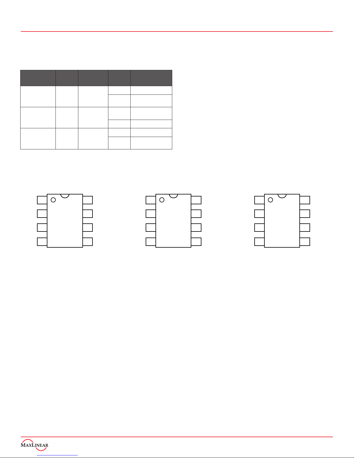
Pin Configurations
1
D
RS
8
1
D
CAN Bus Split Termination - E2, J14, J15, C3, C5, C6, R6
and R9
For CAN Bus split termination, instead of using Table 6,
connect E2 1-5 and 2-5. Populate C3, C5, C6, R6 and R9.
Connect VRxD to J15. J14 can be used for probing.
CAN Bus Transceiver Socket - U2
Provisions are made on the EVB to install a socket (U2) if
desired.
High Transcient Protection - D2
Provisions are made to add high transcient protection (D2)
if desired.
RS
8
1
D
RS
8
GND
VCC
2
3
4
R
7
6
5
CANH
CANL
LBK
GND
VCC
2
3
4
R
Top View, XR31233 Top View, XR31235Top View, XR31234
Figure 3: Pin Configurations for the XR31233, XR31234 and XR31235 CAN Bus Transceivers
7
6
5
CANH
CANL
EN
GND
VCC
2
3
4
R
7
6
5
CAHN
CANL
AB
3/8
Page 4
XR31233 / XR31234 / XR31235 Evaluation Board User’s Manual
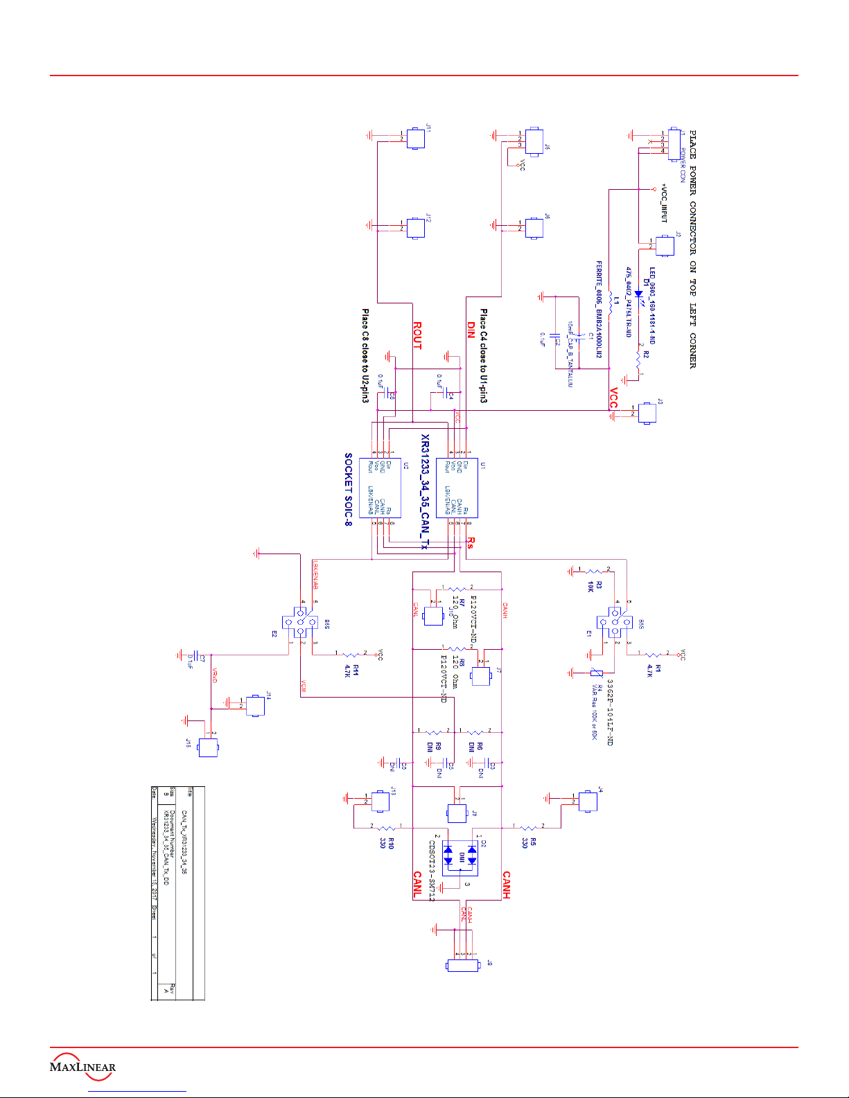
XR31233 / XR31234 / XR31235 EVB Schematic
Figure 4: XR31233 / XR31234 / XR31235 EVB Schematic
4/8
Page 5
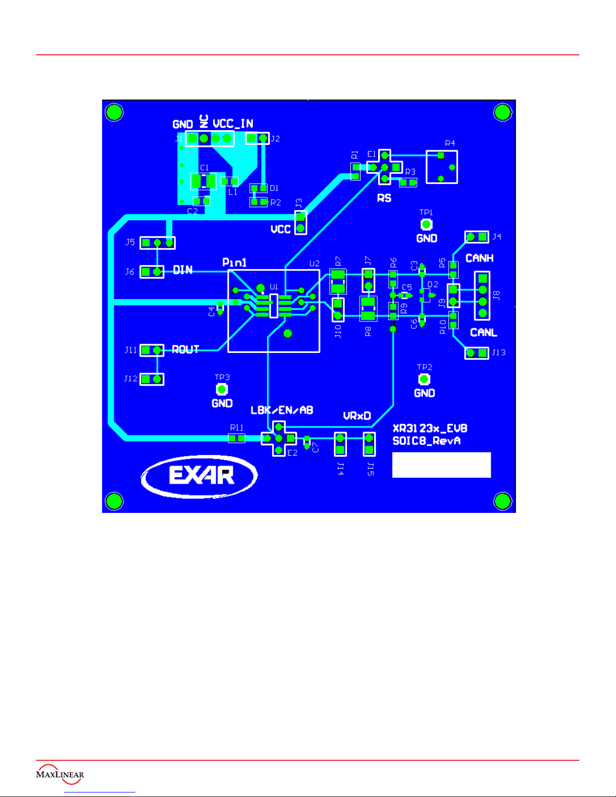
XR31233 / XR31234 / XR31235 Evaluation Board User’s Manual
XR31233 / XR31234 / XR31235 EVB, Top View
Figure 5: XR31233 / XR31234 / XR31235 EVB, Top View
5/8
Page 6
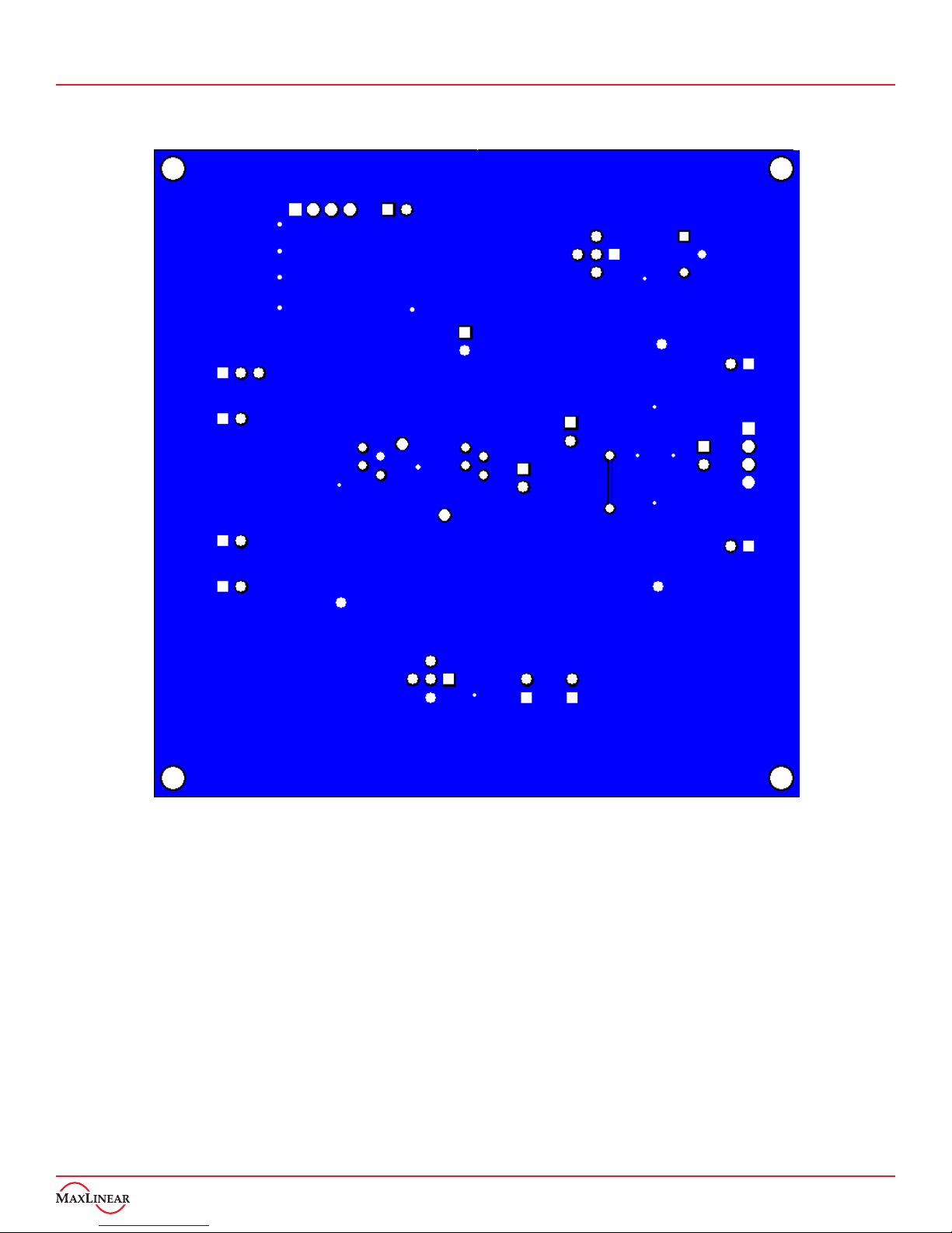
XR31233 / XR31234 / XR31235 Evaluation Board User’s Manual
XR31233 / XR31234 / XR31235 EVB, Bottom View
Figure 5: XR31233 / XR31234 / XR31235 EVB, Bottom View
6/8
Page 7
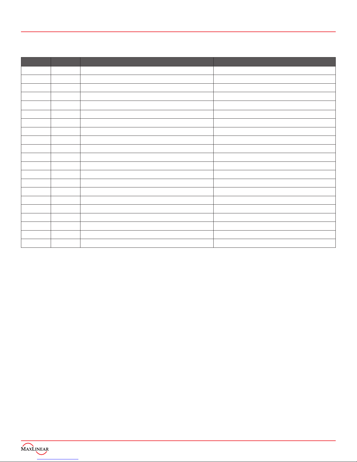
XR31233 / XR31234 / XR31235 Evaluation Board User’s Manual
XR31233 / XR31234 / XR31235 EVB Bill of Materials
Item Quantity Reference Par t
1 1 C1 10mF_CAP_B AVX TAJA106K016RNJ
2 1 C2 0.1uF 0603, 311-1088-1-ND
3 3 C3, C5, C6 Not Stuffed, 0603, 311-1088-1-ND
4 2 C4, C7 0.1uF 0603, 311-1088-1-ND
5 1 D1 LED_0603_160-1181-1-ND
6 1 D2 Not Stuffed, CDSOT23
7 2 J8 HEADER 4 pins
8 12 J2,J3,J4,J6,J7,J9,J10,J11, J12,J13,J14,J15 HEADER 2 pins
9 1 J5 HEADER 3 pins
10 1 L1 FERRITE_0805_ BMB2A1000LN2
11 2 R1, R11 0805 4.7K
12 1 R2 475_0402_P475LTR-ND (475 Ohm)
13 1 R3 0805 10K
14 1 R4 100K/50K TRIMPOT
15 2 R5, R10 0402, 330 Ohm resistor, 311-330JRCT-ND
16 2 R6, R9 Not Stuffed
17 2 R7, R8 1210/0805, 120 Ohm resistor, 311-120GRCT-ND
18 2 E1, E2 B5S CROSSED HEADER
19 1 U1 XR312xx CAN-Tx Sample
20 1 U2 Not Stuffed, SOCKET
21 1 J1 HEADER 4 pins
Table 7: Evaluation Board Bill of Materials (BOM)
7/8
Page 8

XR31233 / XR31234 / XR31235 Evaluation Board User’s Manual
Power Supply Recommendations
In order to ensure reliable operation at all data rates and
supply voltages, each supply should have at least 100nF
ceramic capacitor located as close to the supply terminals
(VCC) as possible. Additional 10uF and 100nF (C1 and C2)
are recommended if the supply source is generated from a
linear power supply/regulator.
Layout Recommendations
1. Apply at least 100nF bypass capacitors as
close as possible to VCC terminal of transceiver.
2. Use at least two vias for VCC and GROUND
connections of bypass capacitors to minimize
effective via-inductance.
3. When possible, use Vcc and GROUND plane
to provide low-inductance traces and signal path.
Corporate Headquarters:
5966 La Place Court
Suite 100
Carlsbad, CA 92008
Tel.:+1 (760) 692-0711
Fax: +1 (760) 444-8598
www.maxlinear.com
The content of this document i s furnish ed for informational u se only, is subj ect to change without notice, a nd should n ot be const rued as a co mmitment by MaxLin ear, Inc.. MaxL inear, Inc. as sumes
no responsibility or liab ility for a ny errors or i naccura cies that m ay appear in the informat ional co ntent cont ained in th is guide. Complyin g with all ap plicable copyright laws is the r esponsibility of the
user. Without limiti ng the rights under copyright , no part of this document may be rep roduce d into, stored in, or introduced into a retrieval sy stem, or transmitte d in any form or by a ny means (elec tronic,
mecha nical, ph otocopyi ng, recor ding, or ot herwis e), or for any purpose, without the expres s written p ermission of MaxLinear, Inc.
Maxli near, Inc. does not r ecommend the u se of any of its prod ucts in life supp ort applic ations where th e failure or malf unction of the p roduct can rea sonably be exp ected to cause fa ilure of the life su pport
system or to s ignificantly af fect its safety or effectiveness. Produ cts are not au thorized for use in suc h applications unl ess MaxLinear, Inc. re ceives, in w riting, a ssuranc es to its sati sfactio n that: (a) the
risk of in jury or da mage has be en minimized; (b) the user assumes all s uch risks; (c) potential liabilit y of MaxLinear, Inc. is ade quately pr otected under the circumsta nces.
MaxLi near, Inc. may have p atents, patent applications, t rademar ks, copyri ghts, or other intellectual property rights covering subj ect matter in this do cument. E xcept as exp ressly pr ovided in any written
license agreeme nt from MaxLinear, Inc., t he furnishing of this d ocument does not gi ve you any lice nse to these patents, tr ademarks, copyrig hts, or othe r intellec tual prop erty.
Company and produ ct names may be registered trademarks or trademarks of t he respective owners with whi ch they are as sociate d.
© 2017 MaxLinear, Inc. All rig hts reser ved
XR31233_XR31234_XR31235 EVB Manual
High Performance Analog:
1060 Rincon Circle
San Jose, CA 95131
Tel.: +1 (669) 265-6100
Fax: +1 (669) 265-6101
Email: [email protected]
www.exar.com
8/8
 Loading...