

Page 1

XR17V354 and XR17V358
Evaluation Board User Manual
TBD/18 001UMR00 i
MaxLinear Confidential
• www.maxlinear.com • 001UMR00
Page 2

XR17V354 and XR17V358 Evaluation Board User Manual Revision History
Revision History
Document No. Release Date Change Description
1.0.1 June 2011 Legacy Exar EVB Manual
001UMR00 November 2018 For updated board - complete re-write.
November 2018 001UMR00 ii
Page 3

XR17V354 and XR17V358 Evaluation Board User Manual Table of Contents
Table of Contents
Introduction......................................................................................................................................................... 1
Reference Documentation .................................................................................................................................1
Ordering Information.......................................................................................................................................... 3
Evaluation Board Overview ............................................................................................................................... 4
MPIO Connections: .......................................................................................................................................................4
SPI Interface:.................................................................................................................................................................4
Transceiver Control Connections: .................................................................................................................................6
System Set-Up / Powering Up ........................................................................................................................... 7
Jumpers.........................................................................................................................................................................7
Pin-out Connectors........................................................................................................................................................7
MPIO Pins and Test Points ...........................................................................................................................................9
Power ............................................................................................................................................................................9
Software ........................................................................................................................................................................9
Software Drivers...................................................................................................................................................9
Windows Device Manager / Port Settings Tab...................................................................................................10
XR17V354 and XR17V358 EVB Schematics ................................................................................................... 11
XR17V354EVB / XR17V358EVB PCB............................................................................................................... 12
XR17V354 / XR17V358 EVB Bill of Materials.................................................................................................. 13
November 2018 001UMR00 iii
Page 4

XR17V354 and XR17V358 Evaluation Board User Manual List of Figures
List of Figures
Figure 1: Top View of the XR17V358IB-E8-EVB.................................................................................................. 1
Figure 2: Bottom View of the XR17V358IB-E8-EVB.............................................................................................2
Figure 3: Top View of the XR17V358IB-0A-EVB.................................................................................................. 2
Figure 4: Bottom View of the XR17V358IB-0A-EVB.............................................................................................2
Figure 5: PCIe and Expansion Interface............................................................................................................... 4
Figure 6: XR17V358IB-E8-EVB Block Diagram ................................................................................................... 5
Figure 7: DB68 Connector.................................................................................................................................... 7
Figure 8: Device Manager / Port Setting tab example........................................................................................ 10
Figure 9: XR17V354 / XR17V358 EVB Top Silkscreen...................................................................................... 12
November 2018 001UMR00 iv
Page 5

XR17V354 and XR17V358 Evaluation Board User Manual List of Tables
List of Tables
Table 1: Evaluation Board Ordering Part Number................................................................................................ 3
Table 2: XRA1405 to SP339 Connections............................................................................................................6
Table 3: Factory Settings...................................................................................................................................... 7
Table 4: DB68 Pin-out .......................................................................................................................................... 8
Table 5: RS485/422 Headers for Each Channel .................................................................................................. 8
Table 6: RS485/422 Header Pin-Out................................................................................................................... 8
Table 7: Test Points.............................................................................................................................................. 9
Table 8: XR17V358IB-0A-EVB Bill of Materials.................................................................................................13
Table 9: XR17V358IB-E8-EVB Bill of Materials..................................................................................................15
Table 10: XR17V354IB-0A-EVB Bill of Materials................................................................................................ 17
November 2018 001UMR00 v
Page 6
XR17V354 and XR17V358 Evaluation Board User Manual Introduction
Introduction
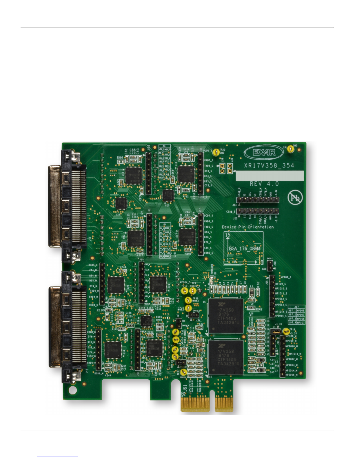
The XR17V354 and XR17V358 evaluation boards provide a platform to evaluate the features and performance of the
XR17V354 and XR17V358. The XR17V354 and XR17V358 are 4-channel and 8-channel PCIe UARTs, respectively. They
are available in the same package and are pin compatible, therefore they utilize the same evaluation board. The evaluation
board revision is 4.0. This user manual gives an overview of the evaluation board and its available configurations. The
available configurations are summarized in the ordering information section.
Please refer to the XR17V354 and XR17V358 datasheets for additional information about these devices.
Reference Documentation
Please refer to the XR17V354 and XR17V358 datasheets for additional information about these devices.
Figure 1: Top View of the XR17V358IB-E8-EVB
November 2018 001UMR00 1
Page 7
XR17V354 and XR17V358 Evaluation Board User Manual Reference Documentation
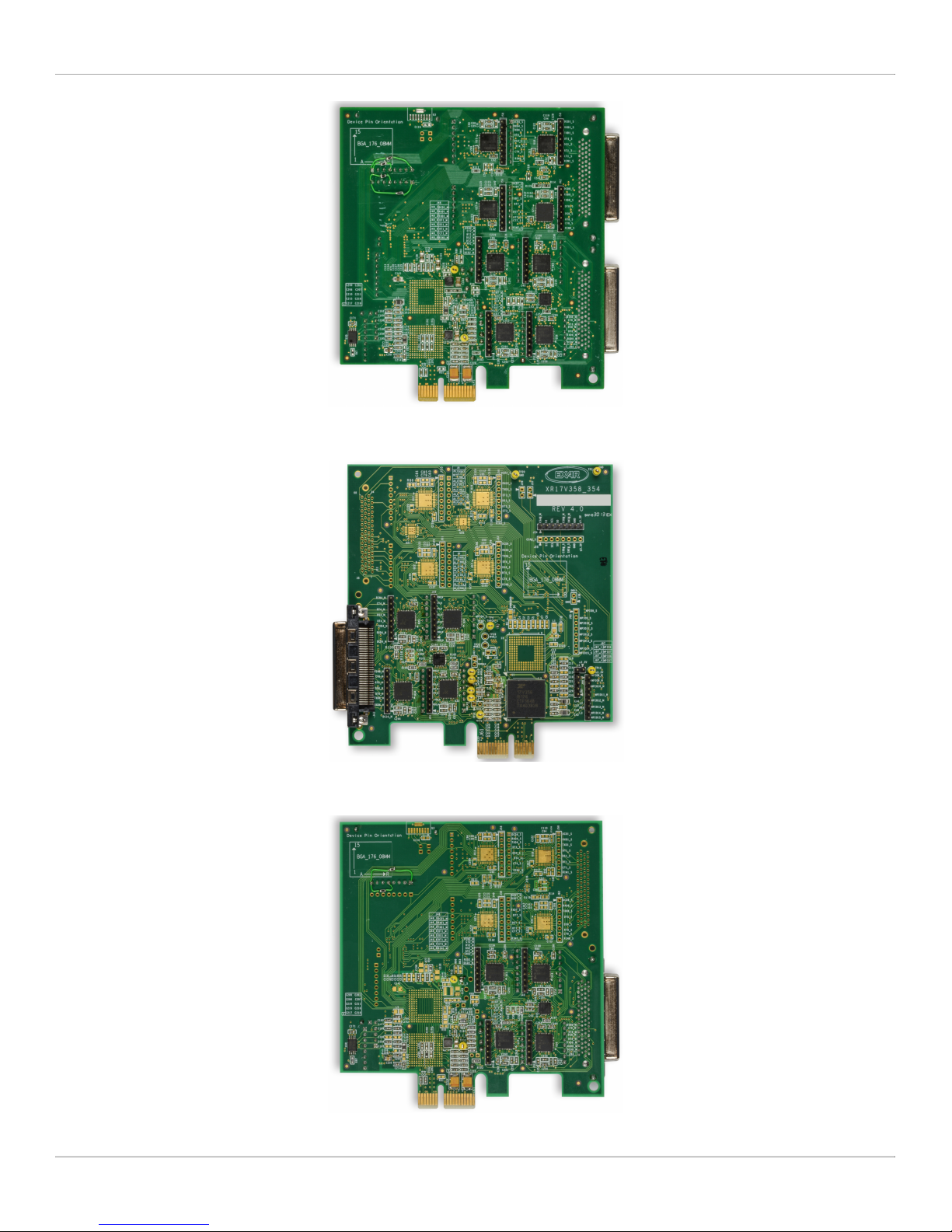
Figure 2: Bottom View of the XR17V358IB-E8-EVB
Figure 3: Top View of the XR17V358IB-0A-EVB
Figure 4: Bottom View of the XR17V358IB-0A-EVB
November 2018 001UMR00 2
Page 8
XR17V354 and XR17V358 Evaluation Board User Manual Ordering Information
Ordering Information
Table 1: Evaluation Board Ordering Part Number
Evaluation Board Description
XR17V354IB-0A-EVB A single 4-channel XR17V354 PCIe UART and four SP339 Transceivers are installed.
XR17V354IB-E4-EVB
XR17V354IB-E8-EVB
XR17V358IB-0A-EVB A single 8-channel XR17V358 PCIe UART and eight SP339 Transceivers are installed.
XR17V358IB-E4-EVB
XR17V358IB-E8-EVB
1. Refer to www.exar.com/XR17V354 and www.exar.com/XR17V358 for most up-to-date Ordering Information.
Two 4-channel XR17V354 PCIe UARTs and eight SP339 Transceivers are installed in a master / slave
configuration.
A master 4-channel XR17V354 PCIe UART, a slave 8-channel XR17V358 PCIe UART and twelve SP339
Transceivers are installed.
A master 8-channel XR17V358 PCIe UART, a slave 4-channel XR17V354 PCIe UART and twelve SP339
Transceivers are installed.
Two 8-channel XR17V358 PCIe UARTs and sixteen SP339 Transceivers are installed in a master / slave
configuration.
November 2018 001UMR00 3
Page 9
XR17V354 and XR17V358 Evaluation Board User Manual Evaluation Board Overview
XR17V358/354
(Master)
XR17V358/3 54
(Slave)
CLK+
CLK-
RX+
RX-
TX+
TX-
D[7:0]
CLK
INT
SEL
MODE
PRES
MODE
PRES
X
4
(
)
XR17V358/354
(Master)
X
(
)
XR17V358/3 54
(Slave)
CLK+
CLK-
RX+
RX-
TX+
TX-
D[7:0]
CLK
INT
SEL
MODE
PRES
MODE
PRES
3.3 V
PCIe Bus
Expansion
Interface
Evaluation Board Overview
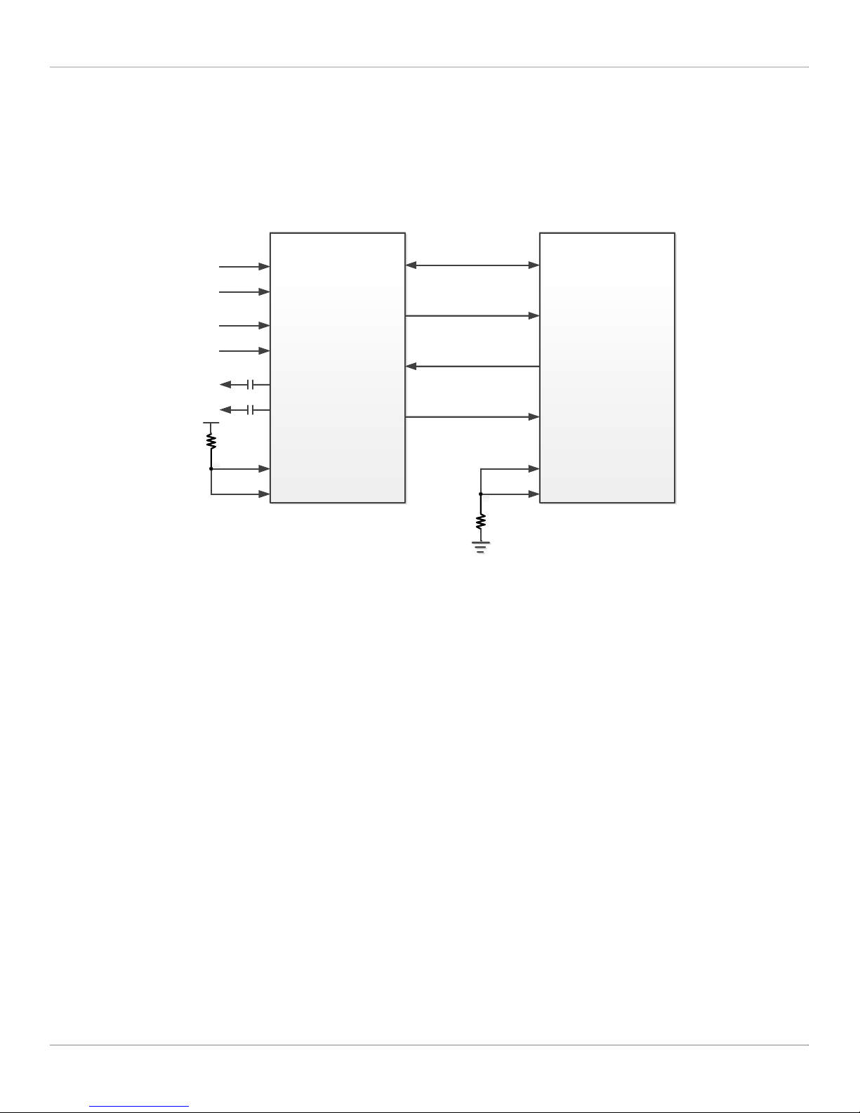
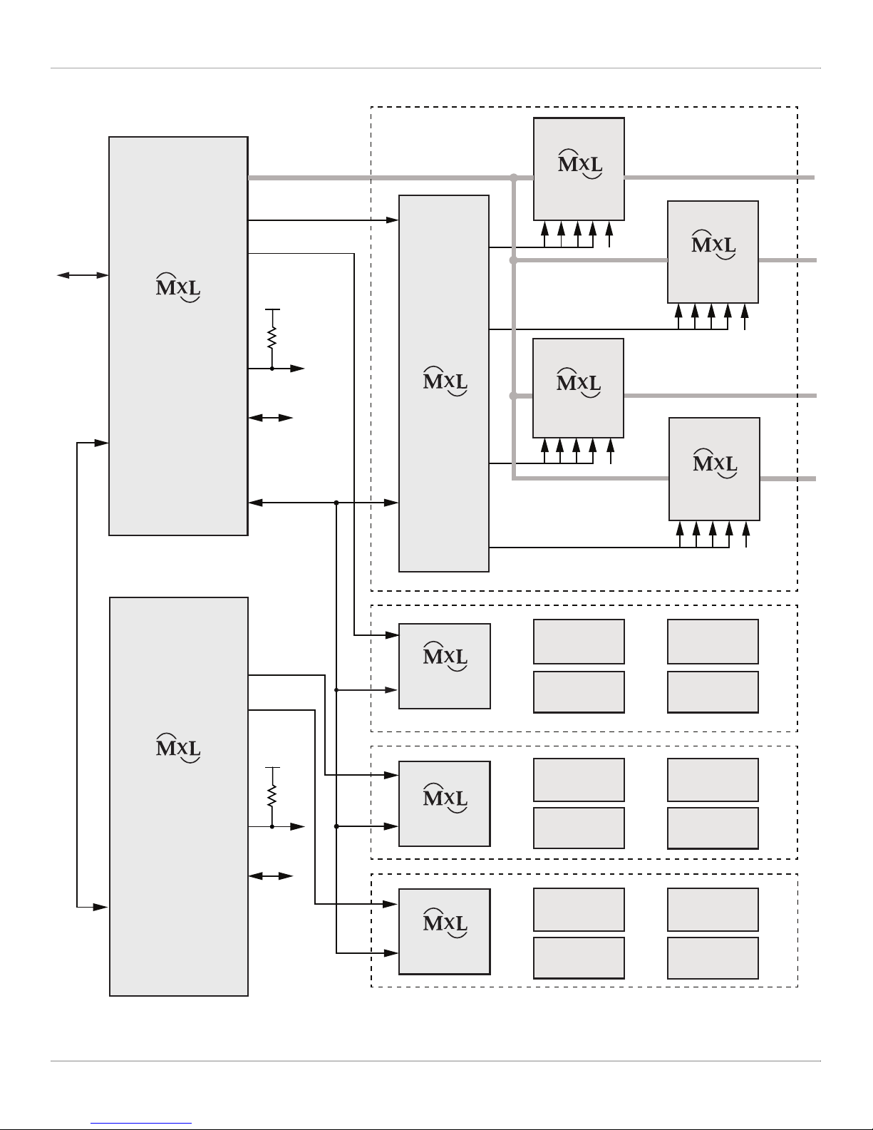
This evaluation board has a x1 PCIe connector and will work in any x1, x4 or x16 PCI slot. Up to 16 UART ports can be
tested on this evaluation board when 2 XR17V358 are installed. The PCI interface of the master device is connected
directly to the PCIe connector. The master device communicates with the slave device via MaxLinear’s proprietary
expansion interface, illustrated in Figure 5. The PCIe interface on the slave device is not used and should be unconnected.
R17V358/35
Master
R17V358/354
Slave
Figure 5: PCIe and Expansion Interface
With the configuration shown below, the XR17V35x Windows device driver allows the Device Manager / Port Settings tab
to control the transceiver modes, slew and termination settings. A block diagram of the XR17V358IB-E8-EVB that uses this
configuration is shown in Figure 6. The device Manager / Port Settings tab is shown in Figure 8.
MPIO Connections:
MPIO3 of both XR17V35x master and slave are pulled-up. Optionally, they connect to the EN pins of their respective
transceivers.
MPIO1 of master XR17V35x is connected to CS of first XRA1405
MPIO2 of master XR17V35x is connected to CS of second XRA1405
MPIO1 of slave XR17V35x is connected to CS of third XRA1405
MPIO2 of slave XR17V35x is connected to CS of fourth XRA1405
Optional: MPIO3 of master is connected to EN pin of transceivers on master ports and MPIO3 of slave is connected to EN
pin of transceivers on slave ports. These MPIO3 pins are pulled up and the Port Settings tab cannot be used to disable the
transceivers.
SPI Interface:
EECK pin of master XR17V35x is connected to SCL pin of all XRA1405
EEDI pin of master XR17V35x is connected to SI pin of all XRA1405
EEDO pin of master XR17V35x is connected to SO pin of all XRA1405
November 2018 001UMR00 4
Page 10
XR17V354 and XR17V358 Evaluation Board User Manual SPI Interface:
PCIe
Bus
Expansion
Interface
Expansion
Interface
XR17V358
Master
XRA1405
XRA1405
Ch 1 SP339
Ch 3 SP339
UART
Channels
1-8
UART
Channels
9-16
EN
TERM
SLEW
MODE1
MODE0
P0-4
P4-7
P8-11
P12-15
Ch 2 SP339
EN
TERM
SLEW
MODE1
MODE0
CS
EN
TERM
SLEW
MODE1
MODE0
Ch 4 SP339
EN
TERM
SLEW
MODE1
MODE0
SPI
Interface
3.3V
EN_M
EN_M
EN_M
EN_M
EN_M
CS
Ch 5 SP339
Ch 6 SP339
Ch 7 SP339 Ch 8 SP339
Ch 9 SP339 Ch 10 SP339
Ch 11 SP339 Ch 12 SP339
Ch 13 SP339 Ch 14 SP339
Ch 15 SP339 Ch 16 SP339
CS
CS
EN_S
(Ch 9-16)
To DB68
EECK
EEDI
EEDO
MPIO4-15
MPIO3
MPIO2
MPIO1
MPIO4-15
MPIO3
MPIO2
MPIO1
SCL
SI
SO
XRA1405
XRA1405
3.3V
Expansion
Interface
XR17V358
Slave
UART
Channels
9-16
MPIO4-15
MPIO3
MPIO2
MPIO1
Figure 6: XR17V358IB-E8-EVB Block Diagram
November 2018 001UMR00 5
Page 11
XR17V354 and XR17V358 Evaluation Board User Manual Transceiver Control Connections:
Transceiver Control Connections:
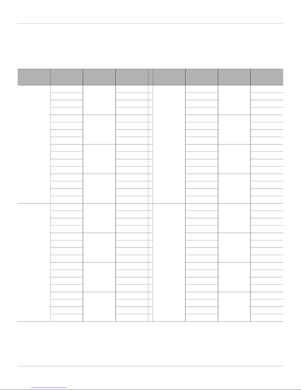
The XRA1405 outputs are sequentially (P0 to P15) connected to the MODE0, MODE1, SLEW and TERM pins of each
SP339 transceiver as shown in Table 2:
Table 2: XRA1405 to SP339 Connections
XRA1405 # XRA1405 Pin
P0
P1 MODE1 P1 MODE1
P2 SLEW P2 SLEW
P3 TERM P3 TERM
P4
P5 MODE1 P5 MODE1
P6 SLEW P6 SLEW
1 (Master)
2 (Master)
P7 TERM P7 TERM
P8
P9 MODE1 P9 MODE1
P10 SLEW P10 SLEW
P11 TERM P11 TERM
P12
P13 MODE1 P13 MODE1
P14 SLEW P14 SLEW
P15 TERM P15 TERM
P0
P1 MODE1 P1 MODE1
P2 SLEW P2 SLEW
P3 TERM P3 TERM
P4
P5 MODE1 P5 MODE1
P6 SLEW P6 SLEW
P7 TERM P7 TERM
P8
P9 MODE1 P9 MODE1
P10 SLEW P10 SLEW
P11 TERM P11 TERM
P12
P13 MODE1 P13 MODE1
P14 SLEW P14 SLEW
P15 TERM P15 TERM
SP339
Channel /
COM Port
1
2
3
4
5
6
7
8
SP339 Pin XRA1405 # XRA1405 Pin
MODE0
MODE0 P4
MODE0 P8
MODE0 P12
MODE0
MODE0 P4
MODE0 P8
MODE0 P12
3 (Slave)
4 (Slave)
P0
P0
SP339
Channel /
COM Port
9
10
11
12
13
14
15
16
SP339 Pin
MODE0
MODE0
MODE0
MODE0
MODE0
MODE0
MODE0
MODE0
November 2018 001UMR00 6
Page 12
XR17V354 and XR17V358 Evaluation Board User Manual System Set-Up / Powering Up
System Set-Up / Powering Up
Jumpers
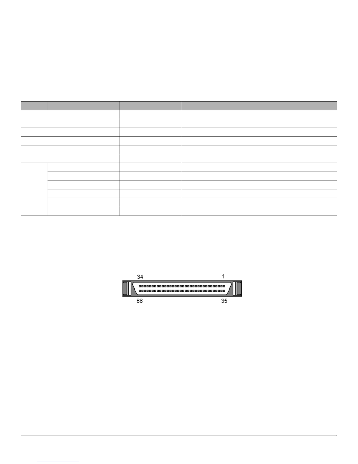
Jumpers are factory installed per Table 3 to configure the EVB for operation. Jumpers may be added or removed per the
description. Refer to the product Data Sheets for additional information.
Table 3: Factory Settings
Jumper Label Factory Setting Description
J1 No jumper Master ENIR# disabled
J41 No jumper Master EN485# disabled
J38 No jumper Slave ENIR# disabled
J32 No jumper Slave EN485# disabled
J37 No jumper Transmit data to IR module not populated
J39 No jumper Receive data to IR module not populated
XR17V354IB-0A-EVB No jumper Master PRES slave not present
XR17V354IB-E4-EVB Jumper 1-2 Master PRES slave present
J4
XR17V354IB-E8-EVB Jumper 1-2 Master PRES slave present
XR17V358IB-0A-EVB No jumper Master PRES slave not present
XR17V358IB-E4-EVB Jumper 1-2 Master PRES slave present
XR17V358IB-E8-EVB Jumper 1-2 Master PRES slave present
Pin-out Connectors
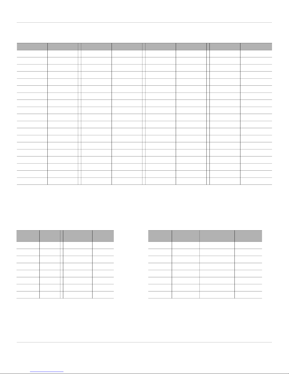
For RS-232 mode, signals on the evaluation board go to the SCSI type ultra micro DB68 connector. Figure 7 shows the
DB68 connector on the board, and Table 4 shows the pin-out. The evaluation boards come with fan-out cables.
Figure 7: DB68 Connector
November 2018 001UMR00 7
Page 13
XR17V354 and XR17V358 Evaluation Board User Manual Pin-out Connectors
Table 4: DB68 Pin-out
Pin Number Signal Name Pin Number Signal Name Pin Number Signal Name Pin Number Signal Name
1 RXD7 18 RXD3 35 RXD8 52 RXD4
2 CT7 19 CT3 36 CT8 53 CT4
3 RIN7 20 RIN3 37 RIN8 54 RIN4
4 RT7 21 RT3 38 RT8 55 RT4
5 DCD7 22 DCD3 39 DCD8 56 DCD4
6 DT7 23 DT3 40 DT8 57 DT4
7 DS7 24 DS3 41 DS8 58 DS4
8 TXD7 25 TXD3 42 TXD8 59 TXD4
9 GND 26 GND 43 GND 60 GND
10 TXD5 27 TXD1 44 TXD6 61 TXD2
11 DS5 28 DS1 45 DS6 62 DS2
12 DT5 29 DT1 46 DT6 63 DT2
13 DCD5 30 DCD1 47 DCD6 64 DCD2
14 RT5 31 RT1 48 RT6 65 RT2
15 RIN5 32 RIN1 49 RIN6 66 RIN2
16 CT5 33 CT1 50 CT6 67 CT2
17 RXD5 34 RXD1 51 RXD6 68 RXD2
For RS-422/485 mode, signals on the evaluation board go to headers. Table 5 shows the header name for each channel;
Table 6 shows the pin-out used for each RS485/422 header.
Table 5: RS485/422 Headers for Each Channel
Channel
Number
Master 1 J48 9 (Slave 1) J50
Master 2 J49 10 (Slave 2) J55
Master 3 J89 11 (Slave 3) J56
Master 4 J90 12 (Slave 4) J58
Master 5 J91 13 (Slave 5) J51
Master 6 J92 14 (Slave 6) J57
Master 7 J93 15 (Slave 7) J59
Master 8 J94 16 (Slave 8) J62
Header
Number
Channel
Number
Header
Number
Table 6: RS485/422 Header Pin-Out
Pin
Number
1 TX- / RX- TX- DCD
2 TX+ / RX+ TX+ RXD
3 - RX+ TXD
4 - RX- DT
5 - - DS
6 - - RT
7 - - CT
8 - - RIN
RS485
Half Duplex
RS485 / RS422
Full Duplex
RS-232
Test Point
November 2018 001UMR00 8
Page 14
XR17V354 and XR17V358 Evaluation Board User Manual MPIO Pins and Test Points
MPIO Pins and Test Points
The MPIO pins of both the master and slave devices are connected to test points or test headers on the evaluation board.
Refer to page 6 of the evaluation board schematic and Table 7 below for details. Note that an external pullup is
recommended for each unused MPIO pins configured as an input.
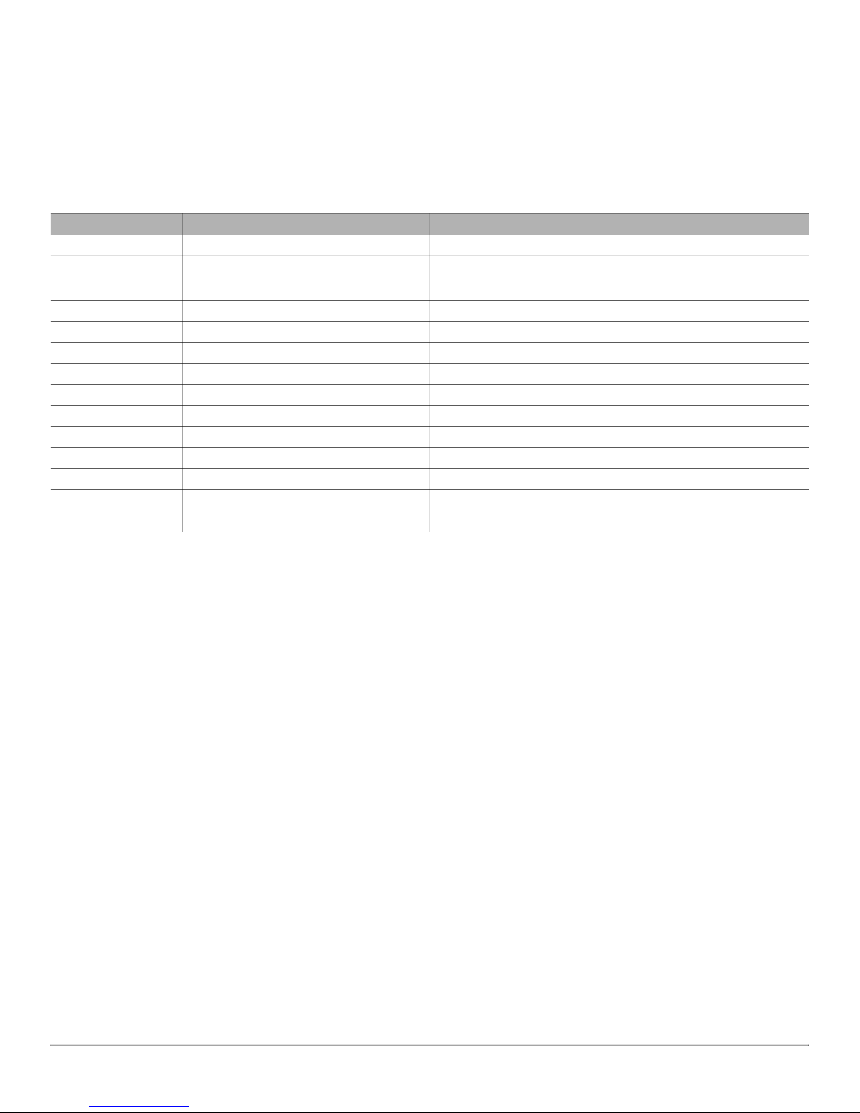
Table 7: Test Points
TP# Signal Description
TP1 GND Digital Ground
TP4 TRMCK (Slave) Timer / counter external clock input
TP16 +3.3V V
TP20 GND Digital Ground
TP27 TMRCK (Master) Timer / counter external clock input
TP31 PERST# PCIe System Reset
TP32 1V2 Buck Output (Master) Regulated 1.2 V output
TP33 1V2 Buck Output (Slave) Regulated 1.2 V output
TP34 MPIO0 (Master) Timer output (when enabled)
TP35 MPIO0 (Slave) Timer output (when enabled)
TP36 MPIO4 (Master) General Purpose MPIO Test Point
TP37 MPIO5 (Master) General Purpose MPIO Test Point
TP38 MPIO4 (Slave) General Purpose MPIO Test Point
TP39 MPIO5 (Slave) General Purpose MPIO Test Point
CC
Power
Power is connected when the PCIe board is plugged into the computer’s PCIe bus. Each XR17V354 and XR17V358 has
an internal buck regulator that is powered by the PCIe bus 3.3V supply and produces a 1.2V output. This 1.2V output may
be used to drive the 1.2V power required by the same XR17V35x, or alternatively the 1.2V may be supplied externally. If
using an external 1.2V supply, a 250ohm pull-down resistor is recommended on the VCC12 pin per the January 2012
Errata.
The PWRGD of each XR17V35x illuminates an LED when its buck regulator is within regulation.
Software
Software Drivers
Custom software drivers for Windows and Linux are available from MaxLinear at www.exar.com/design-tools/software-
drivers. For Linux, please refer to Application Note AN-225 Installing and Testing a PCI / PCIe UART Serial Port Using a
Custom MaxLinear Driver in Linux.
November 2018 001UMR00 9
Page 15
XR17V354 and XR17V358 Evaluation Board User Manual Software
Windows Device Manager / Port Settings Tab
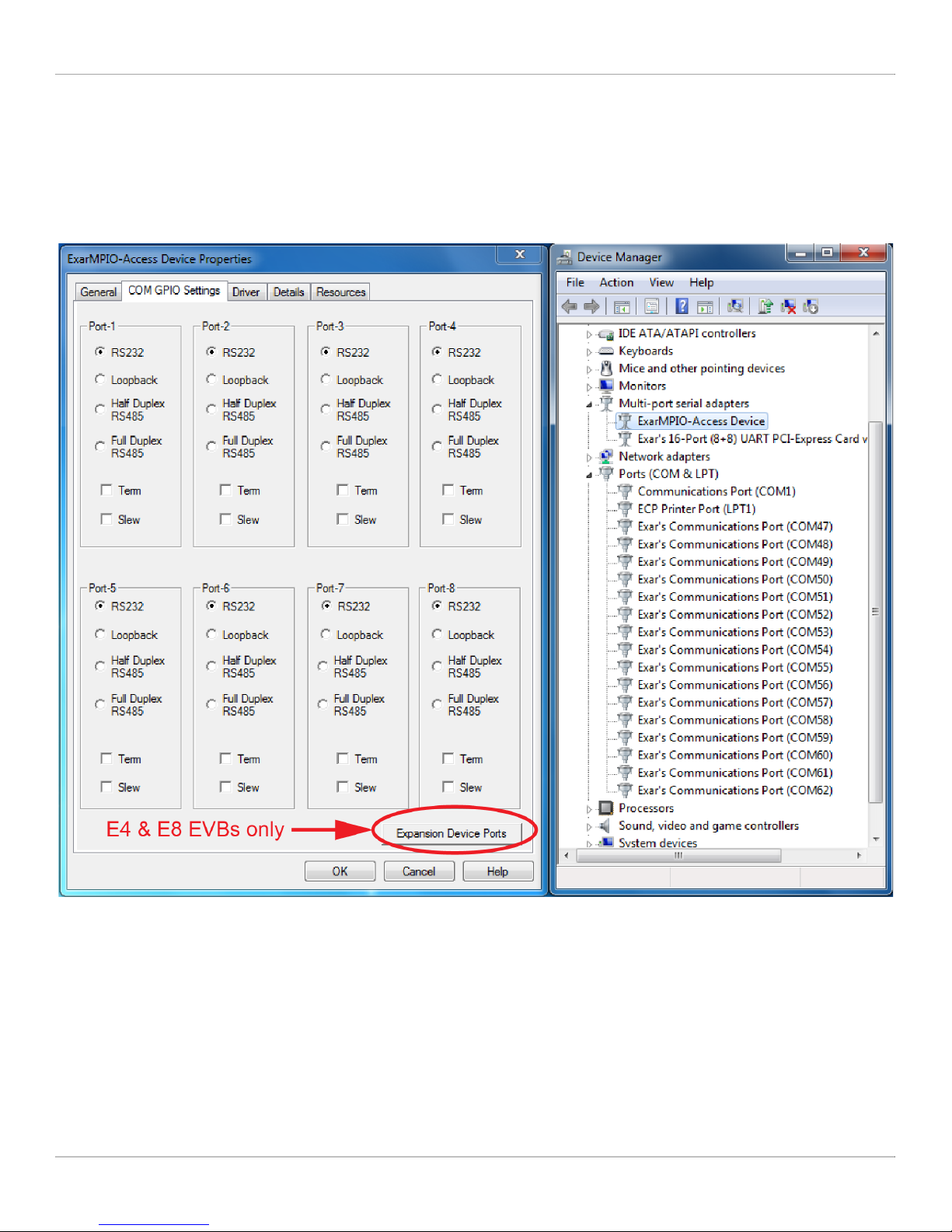
After loading the Windows driver, access the Device Manager as shown in Figure 8 (right side). From there, open the
ExarMPIO-Access Device as shown in Figure 8 (left side) to see the Port Settings. Here the transceiver mode, slew rate
and RS-485 receiver termination enable can be selected. See the SP339E datasheet for more. Click on the Expansion
Device Ports button on the lower right to see the slave ports for E4 and E8 EVBs. For 0A EVBs, there are no Expansion
Device Ports.
1. Loopback mode occurs at the transceiver, not at the UART.
2. Slew control applies to RS-232, RS485 Half and Full Duplex. Term applies to RS-485 Half and Full Duplex. See SP339 datasheet for more.
Figure 8: Device Manager / Port Setting tab example
After the ports are set, they can be tested using any serial testing tool or MaxLinear’s Super GUI which can be found from
the XR17V358 product page, under Design Tools / Evaluation Hardware and Software, Software Drivers.
Please note: When designing your own board, all hardware connections listed in the Evaluation Board Overview section
are required for the MaxLinear custom driver to enable the COM GPIO settings in Figure 8. If any of these connections are
missing, this tab will be blank.
November 2018 001UMR00 10
Page 16

XR17V354 and XR17V358 Evaluation Board User Manual XR17V354 and XR17V358 EVB Schematics
XR17V354 and XR17V358 EVB Schematics
The schematic for the XR17V358IB-E8-EVB can be found on www.exar.com/XR17V358 under the documentation tab,
under schematics. The XR17V358IB-0A-EVB uses the same schematic, except the slave components are not populated.
The XR17V358IB-E4-EVB uses the same schematic, except the slave PCIe UART is the XR17V354 (the XR17V358 is pin
compatible to the XR17V354) and the transceivers for channels 5-8 are not populated.
For the XR17V354 EVBs, again the pin compatibility with the XR17V358 is used. The slave components on the
XR17V354IB-0A-EVB are not populated, the XR17V354 is installed as the master and the master‘s channel 5-8
transceivers are not populated. For the XR17V354IB-E4-EVB, a master XR17V354 and a slave XR17V354 is installed;
channel 5-8 transceivers are not populated. For the XR17V354IB-E8-EVB, a master XR17V354 is installed and its channel
5-8 transceivers are not populated.
See the Bill of Materials section for more regarding populated components for XR17V354IB-0A-EVB, XR17V358IB-0AEVB and XR17V358IB-E8-EVB. See product page for design guidelines for the XR17V354 and XR17V358.
November 2018 001UMR00 11
Page 17
XR17V354 and XR17V358 Evaluation Board User Manual XR17V354EVB / XR17V358EVB PCB
XR17V354EVB / XR17V358EVB PCB
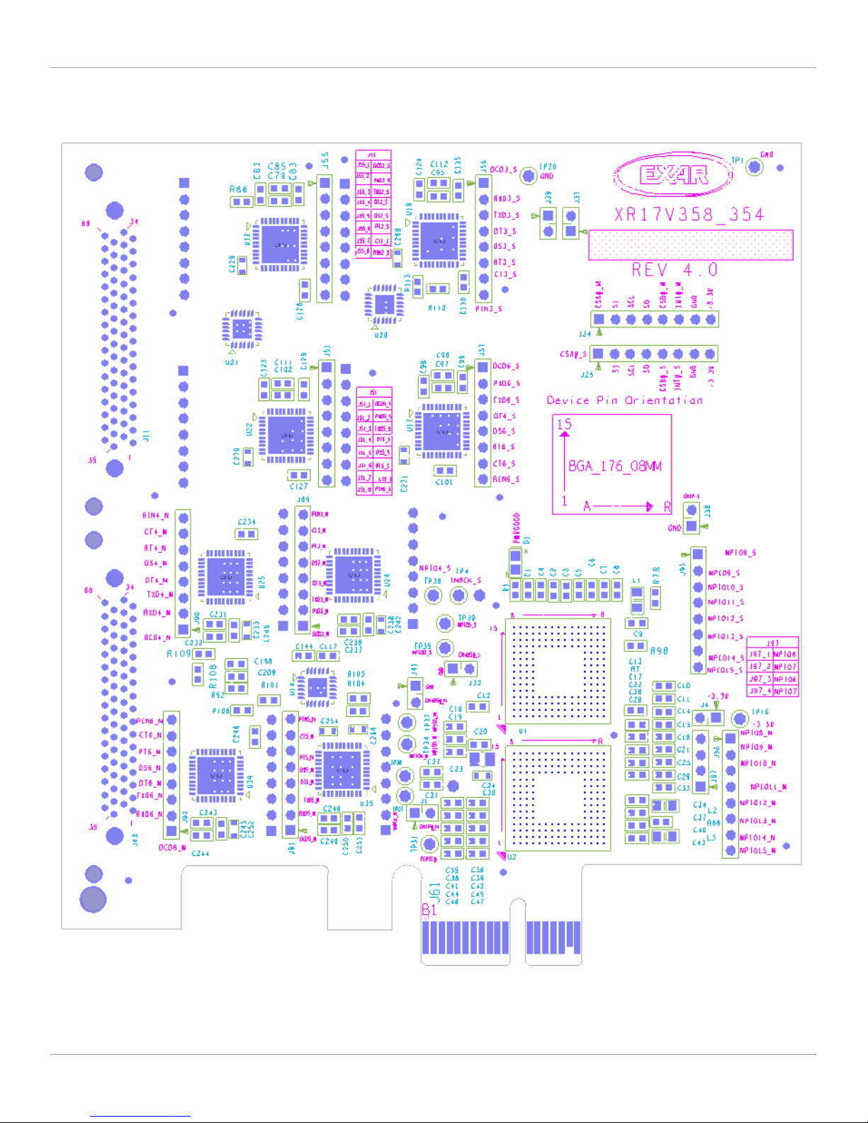
Figure 9: XR17V354 / XR17V358 EVB Top Silkscreen
November 2018 001UMR00 12
Page 18
XR17V354 and XR17V358 Evaluation Board User Manual XR17V354 / XR17V358 EVB Bill of Materials
XR17V354 / XR17V358 EVB Bill of Materials
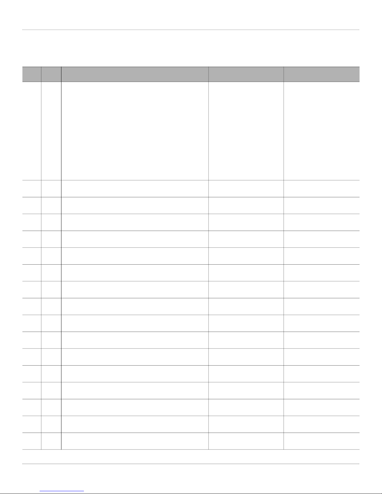
Table 8: XR17V358IB-0A-EVB Bill of Materials
Item Qty Reference Designator Description
1 97 C11, C12, C13, C14, C16, C17, C18, C19, C20, C21,
C22, C23, C27, C28, C29, C31, C35, C36, C37, C38,
C39, C40, C41, C42, C43, C44, C45, C46, C47, C48,
C49, C50, C51, C52, C53, C78, C79, C80, C82, C84,
C86, C88, C93, C100, C104, C106, C108, C117, C121,
C136, C138, C144, C152, C160, C161, C162, C165,
C168, C169, C171, C174, C177, C178, C183, C186,
C187, C189, C191, C192, C193, C196, C198, C200,
C201, C203, C204, C205, C206, C207, C209, C210,
C211, C214, C215, C216, C217, C218, C231, C232,
C233, C234, C235, C236, C237, C238, C239, C241,
C243, C244, C245, C246, C247, C248, C249, C250,
C251, C253, C255, C256, C257, C258, C259, C260,
C261, C262, C263, C265
2 3 C24, C30, C208 CAP CER 10UF 6.3V X5R
3 1 C188 CAP CER 47UF 6.3V X5R
4 1 C219, C220 CAP TANT 10UF 16V 10%
5 8 C228, C230, C240, C242, C252, C254, C264, C266 CAP CER 1UF 16V X7R
6 1 D17 LED RED CLEAR CHIP
7 5 J1, J4, J41 CONN HEADER 2MM
8 1 J43 CONN CHAMP RECPT
9 10 J24, J48, J49, J89, J90, J91, J92, J93, J94, J96 CONN HEADER 2MM
10 1 J97 CONN HEADER 2MM
11 3 L2, L3, L6 FERRITE BEAD 1 KOHM
12 1 L7 FIXED IND 4.7UH 1A 200
13 1 R84 RES SMD 475 OHM 1%
14 16 R7, R97, R100, R101, R104, R105, R106, R107, R108,
R109, R54, R87, R88, R91, R99, R103
15 1 R102 RES SMD 191 OHM 1%
16 11 TP1, TP4, TP16, TP20, TP27, TP31, TP32, TP33, TP34,
TP36, TP37
17 1 U2 Octal PCI Express UART MaxLinear
CAP CER 0.1UF 16V X7R
0402
0603
0805
1411
0603
SMD 0603
SINGLE STR 2 POS
RTANG 68POS PCB
SINGLE STR 8 POS
SINGLE STR 4POS
0805 1LN
MOHM SMD
1/10W 0402
RES SMD 4.7K OHM 1%
1/10W 0402
1/10W 0402
TEST POINT PC MINI
.040"D YELLOW
Manufacturer / Part
Number
Wurth
885012205037
Wurth
855012106006
Wurth
885012107006
Kemet
T491B106K016AT
Wurth
885012206076
Lite-on
LTST-C190CKT
Wurth
62000211121
TE Connectivity, Amp
5796055-1
Wurth
62000811121
Wurth
62000411121
Wurth
742792096
Wurth
744029004
Panasonic
ERJ-2RKF4750X
Panasonic
ERJ-2RKF4701X
Panasonic
ERJ-2RKF1910X
Keystone
5004
XR17V358IB176-F
November 2018 001UMR00 13
Page 19
XR17V354 and XR17V358 Evaluation Board User Manual XR17V354 / XR17V358 EVB Bill of Materials
Table 8: (Continued)XR17V358IB-0A-EVB Bill of Materials
Item Qty Reference Designator Description
18 8 U11, U16, U24, U25, U34, U35, U36, U37 RS232/RS485/RS422
Transceiver with
Internal Termination
19 2 U14, U15 XRA1405_QFN24 MaxLinear
20 1 U30 IC EEPROM 1K SPI 2MHZ
8TSSOP
Manufacturer / Part
Number
MaxLinear
SP339EER1-L
XRA1405IL24-F
Microchip
AT93C46E-TH-B
November 2018 001UMR00 14
Page 20
XR17V354 and XR17V358 Evaluation Board User Manual XR17V354 / XR17V358 EVB Bill of Materials
Table 9: XR17V358IB-E8-EVB Bill of Materials
Item Qty Reference Designator Description
1 185 C1, C2, C3, C4, C5, C6, C7, C8, C9, C10, C11, C12, C13,
C14, C15, C16, C17, C18, C19, C20, C21, C22, C23,
C25, C26, C27, C28, C29, C31, C33, C34, C35, C36,
C37, C38, C39, C40, C41, C42, C43, C44, C45, C46,
C47, C48, C49, C50, C51, C52, C53, C54, C55, C56,
C57, C78, C79, C80, C81, C82, C83, C84, C85, C86,
C87, C88, C89, C90, C91, C92, C93, C94, C95, C96,
C97, C98, C99, C100, C101, C102, C103, C104, C105,
C106, C107, C108, C109, C110, C111, C112, C113,
C114, C115, C117, C121, C122, C123, C124, C125,
C126, C127, C128, C129, C130, C132, C133, C134,
C135, C136, C137, C138, C139, C140, C144, C152,
C160, C161, C162, C163, C164, C165, C166, C168,
C169, C171, C174, C177, C178, C180, C182, C183,
C186, C187, C189, C191, C192, C193, C195, C196,
C198, C199, C200, C201, C203, C204, C205, C206,
C207, C209, C210, C211, C214, C215, C216, C217,
C218, C231, C232, C233, C234, C235, C236, C237,
C238, C239, C241, C243, C244, C245, C246, C247,
C248, C249, C250, C251, C253, C255, C256, C257,
C258, C259, C260, C261, C262, C263, C265
2 6 C24, C30, C131, C141, C158, C208 CAP CER 10UF 6.3V X5R
3 2 C143, C188 CAP CER 47UF 6.3V X5R
4 2 C219, C220 CAP TANT 10UF 16V 10%
5 16 C228, C229, C230, C240, C242, C252, C254, C264,
C266, C267, C268, C269, C270, C271, C272, C273
6 2 D1, D17 LED RED CLEAR CHIP
7 5 J1, J4, J32, J38, J41 CONN HEADER 2MM
8 2 J11, J43 CONN CHAMP RECPT
9 20 J24, J25, J48, J49, J50, J51, J55, J56, J57, J58, J59, J62,
J89, J90, J91, J92, J93, J94, J95, J96
10 1 J97 CONN HEADER 2MM
11 6 L1, L2, L3, L5, L6, L8 FERRITE BEAD 1 KOHM
12 2 L4, L7 FIXED IND 4.7UH 1A 200
13 2 R1, R84 RES SMD 475 OHM 1%
14 29 R7, R97, R98, R100, R101, R104, R105, R106, R107,
R108, R109, R110, R111, R112, R113, R114, R115,
R116, R117, R54, R83, R87, R88, R89, R90, R91, R92,
R99, R103
CAP CER 0.1UF 16V X7R
0402
0603
0805
1411
CAP CER 1UF 16V X7R
0603
SMD 0603
SINGLE STR 2 POS
RTANG 68POS PCB
CONN HEADER 2MM
SINGLE STR 8 POS
SINGLE STR 4POS
0805 1LN
MOHM SMD
1/10W 0402
RES SMD 4.7K OHM 1%
1/10W 0402
Manufacturer / Part
Number
Wurth
885012205037
Wurth
855012106006
Wurth
885012107006
Kemet
T491B106K016AT
Wurth
885012206076
Lite-on
LTST-C190CKT
Wurth
62000211121
TE Connectivity, Amp
5796055-1
Wurth
62000811121
Wurth
62000411121
Wurth
742792096
Wurth
744029004
Panasonic
ERJ-2RKF4750X
Panasonic
ERJ-2RKF4701X
November 2018 001UMR00 15
Page 21
XR17V354 and XR17V358 Evaluation Board User Manual XR17V354 / XR17V358 EVB Bill of Materials
Table 9: XR17V358IB-E8-EVB Bill of Materials
Item Qty Reference Designator Description
15 1 R102 RES SMD 191 OHM 1%
1/10W 0402
16 14 TP1, TP4, TP16, TP20, TP27, TP31, TP32, TP33, TP34,
TP35, TP36, TP37, TP38, TP39
17 1 U1 Octal PCI Express UART
18 1 U2 Octal PCI Express UART
19 16 U11, U12, U13, U16, U17, U18, U19, U22, U23, U24,
U25, U27, U34, U35, U36, U37
20 4 U14, U15, U20, U21 XRA1405_QFN24
21 1 U30 IC EEPROM 1K SPI 2MHZ
TEST POINT PC MINI
.040"D YELLOW
RS232/RS485/RS422
Transceiver with
Internal Termination
8TSSOP
Manufacturer / Part
Number
Panasonic
ERJ-2RKF1910X
Keystone
5004
MaxLinear
XR17V358IB176-F
MaxLinear
XR17V358IB176-F
MaxLinear
SP339EER1-L
MaxLinear
XRA1405IL24-F
Microchip
AT93C46E-TH-B
November 2018 001UMR00 16
Page 22
XR17V354 and XR17V358 Evaluation Board User Manual XR17V354 / XR17V358 EVB Bill of Materials
Table 10: XR17V354IB-0A-EVB Bill of Materials
Item Qty Reference Designator Description Manufacturer / Part Number
1 90 C11, C12, C13, C14, C16, C17, C18, C19, C20, C21,
C22, C23, C27, C28, C29, C31, C35, C36, C37, C38,
C39, C40, C41, C42, C43, C44, C45, C46, C47, C48,
C49, C50, C51, C78, C80, C82, C84, C86, C93, C100,
C104, C106, C108, C117, C121, C144, C152, C161,
C162, C165, C168, C169, C171, C174, C177, C178,
C183, C186, C187, C189, C191, C192, C193, C196,
C198, C200, C201, C203, C204, C205, C206, C207,
C209, C210, C211, C214, C215, C216, C217, C218,
C231, C232, C233, C234, C235, C236, C237, C238,
C239, C241
2 3 C24, C30, C208 CAP CER 10UF 6.3V X5R
3 1 C188 CAP CER 47UF 6.3V X5R
4 2 C219, C220 CAP TANT 10UF 16V 10%
5 4 C228, C230, C240, C242 CAP CER 1UF 16V X7R
6 1 D17 LED RED CLEAR CHIP
7 5 J1, J4, J41 CONN HEADER 2MM
8 1 J43 CONN CHAMP RECPT
9 6 J24, J48, J49, J89, J90, J96 CONN HEADER 2MM
10 1 J97 CONN HEADER 2MM
11 3 L2, L3, L6 FERRITE BEAD 1 KOHM
12 1 L7 FIXED IND 4.7UH 1A 200
13 1 R84 RES SMD 475 OHM 1%
14 15 R7, R97, R100, R101, R104, R105, R54, R87, R88, R91,
R99, R103
15 1 R102 RES SMD 191 OHM 1%
16 11 TP1, TP16, TP20, TP27, TP31, TP32, TP34, TP36, TP37 TEST POINT PC MINI
17 1 U2 Quad PCI Express UART
18 4 U11, U16, U24, U25 RS232/RS485/RS422
CAP CER 0.1UF 16V X7R
0402
0603
0805
1411
0603
SMD 0603
SINGLE STR 2 POS
RTANG 68POS PCB
SINGLE STR 8 POS
SINGLE STR 4POS
0805 1LN
MOHM SMD
1/10W 0402
RES SMD 4.7K OHM 1%
1/10W 0402
1/10W 0402
.040"D YELLOW
Transceiver with
Internal Termination
Wurth
885012205037
Wurth
855012106006
Wurth
885012107006
Kemet
T491B106K016AT
Wurth
885012206076
Lite-on
LTST-C190CKT
Wurth
62000211121
TE Connectivity, Amp
5796055-1
Wurth
62000811121
Wurth
62000411121
Wurth
742792096
Wurth
744029004
Panasonic
ERJ-2RKF4750X
Panasonic
ERJ-2RKF4701X
Panasonic
ERJ-2RKF1910X
Keystone
5004
MaxLinear
XR17V354IB176-F
MaxLinear
SP339EER1-L
November 2018 001UMR00 17
Page 23
XR17V354 and XR17V358 Evaluation Board User Manual Disclaimer
Table 10: XR17V354IB-0A-EVB Bill of Materials
Item Qty Reference Designator Description Manufacturer / Part Number
19 3 U14 XRA1405_QFN24
20 1 U30 IC EEPROM 1K SPI 2MHZ
8TSSOP
MaxLinear
XRA1405IL24-F
Microchip
AT93C46E-TH-B
MaxLinear, Inc.
5966 La Place Court, Suite 100
Carlsbad, CA 92008
760.692.0711 p.
760.444.8598 f.
www.maxlinear.com
The content of this document is furnished for informational use only, is subject to change without notice, and should not be construed as a commitment by
MaxLinear, Inc. MaxLinear, Inc. assumes no responsibility or liability for any errors or inaccuracies that may appear in the informational content contained in this
guide. Complying with all applicable copyright laws is the responsibility of the user. Without limiting the rights under copyright, no part of this document may be
reproduced into, stored in, or introduced into a retrieval system, or transmitted in any form or by any means (electronic, mechanical, photocopying, recording, or
otherwise), or for any purpose, without the express written permission of MaxLinear, Inc.
Maxlinear, Inc. does not recommend the use of any of its products in life support applications where the failure or malfunction of the product can reasonably be
expected to cause failure of the life support system or to significantly affect its safety or effectiveness. Products are not authorized for use in such applications unless
MaxLinear, Inc. receives, in writing, assurances to its satisfaction that: (a) the risk of injury or damage has been minimized; (b) the user assumes all such risks; (c)
potential liability of MaxLinear, Inc. is adequately protected under the circumstances.
MaxLinear, Inc. may have patents, patent applications, trademarks, copyrights, or other intellectual property rights covering subject matter in this document. Except
as expressly provided in any written license agreement from MaxLinear, Inc., the furnishing of this document does not give you any license to these patents,
trademarks, copyrights, or other intellectual property.
MaxLinear, the MaxLinear logo, and any MaxLinear trademarks, MxL, Full-Spectrum Capture, FSC, G.now, AirPHY and the MaxLinear logo are all on the products
sold, are all trademarks of MaxLinear, Inc. or one of MaxLinear’s subsidiaries in the U.S.A. and other countries. All rights reserved. Other company trademarks and
product names appearing herein are the property of their respective owners.
© 2018 MaxLinear, Inc. All rights reserved.
 Loading...