

Page 1
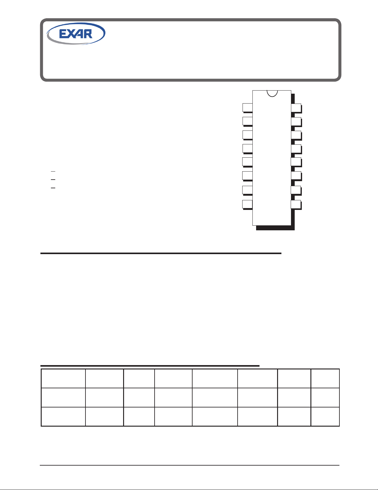
SP3222EB/SP3232EB
True +3.0V to +5.5V RS-232 Transceivers
The SP3222EB/SP3232EB series is an RS-232 transceiver solution intended for portable or
hand-held applications such as notebook or laptop computers. The SP3222EB/SP3232EB
series has a high-effi ciency, charge-pump power supply that requires only 0.1µF capacitors
in 3.3V operation. This charge pump allows the SP3222EB/SP3232EB series to deliver true
RS-232 performance from a single power supply ranging from +3.0V to +5.5V. The SP3222EB/
SP3232EB are 2-driver/2-receiver devices. The ESD tolerance of the SP3222EB/SP3232EB
devices is over +/-15kV for both Human Body Model and IEC61000-4-2 Air discharge test
methods. The SP3222EB device has a low-power shutdown mode where the devices' driver
outputs and charge pumps are disabled. During shutdown, the supply current falls to less
than 1µA.
FEATURES
■ Meets true EIA/TIA-232-F Standards
from a +3.0V to +5.5V power supply
■ 250kbps Transmission Rate Under Load
■ 1µA Low Power Shutdown with
Receivers active (SP3222EB)
■ Interoperable with RS-232 down to a
+2.7V power source
■ Enhanced ESD Specifi cations:
+15kV Human Body Model
+15kV IEC61000-4-2 Air Discharge
+8kV IEC61000-4-2 Contact Discharge
DESCRIPTION
SELECTION TABLE
Now Available in Lead Free Packaging
V-
1
2
3
4
13
14
15
16
5
6
7
12
11
10
C1+
V+
C1-
C2+
C2-
R1IN
R2IN
GND
V
CC
T1OUT
T2IN
8
9
SP3232EB
T1IN
R1OUT
R2OUT
T2OUT
Device Power
Supplies
RS-232
Drivers
RS-232
Receivers
External
Components
Shutdown TTL
3-State
# of
Pins
SP3222EB +3.0V to
+5.5V
2 2 4 Capacitors Yes Yes 18, 20
SP3232EB +3.0V to
+5.5V
2 2 4 Capacitors No No 16
Exar Corporation 48720 Kato Road, Fremont CA, 94538 • 510-668-7017 • www.exar.com SP3222EB/SP3232EB_104_052615
1
Page 2
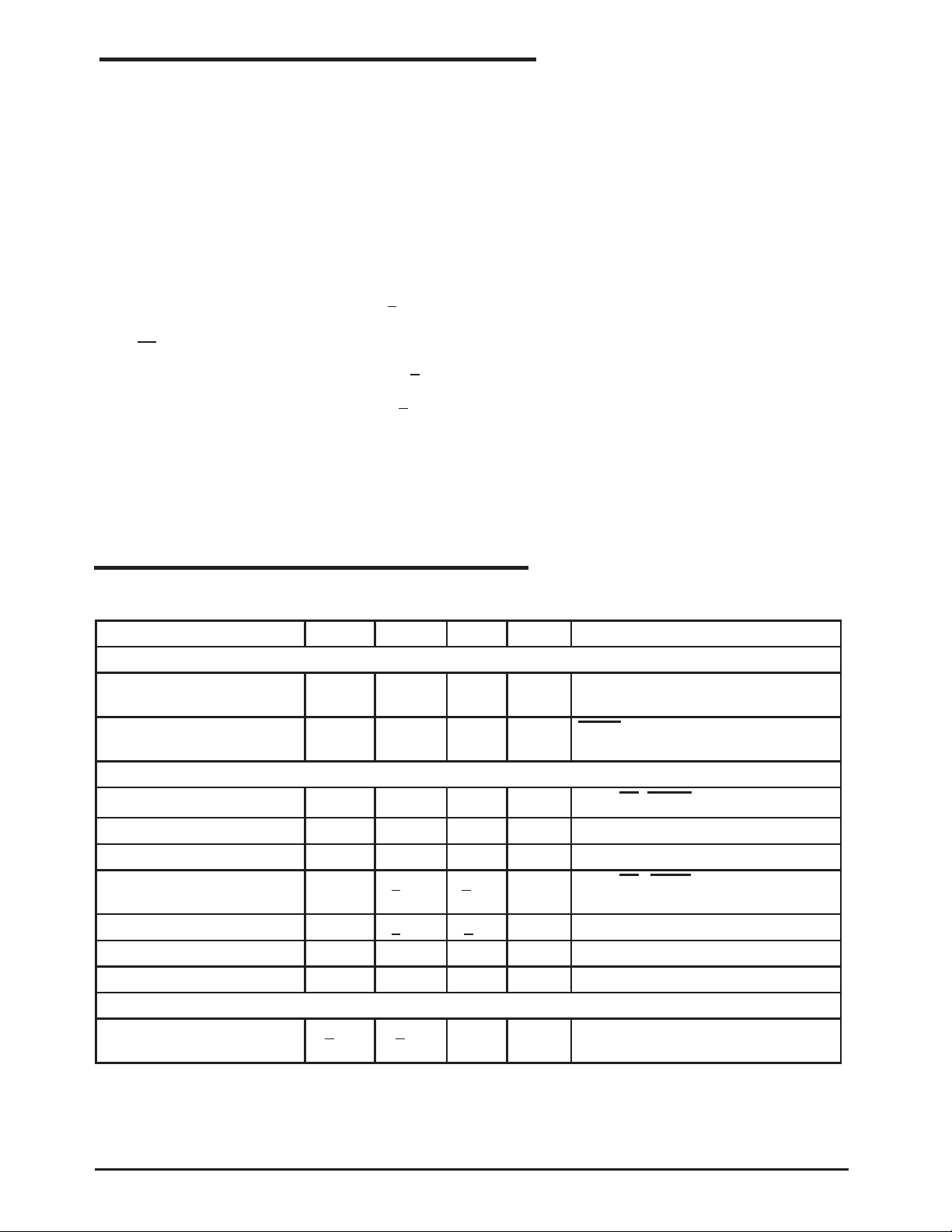
NOTE 1: V+ and V- can have maximum magnitudes of 7V, but their absolute difference cannot exceed 13V.
These are stress ratings only and functional operation
of the device at these ratings or any other above those
indicated in the operation sections of the specifi cations
below is not implied. Exposure to absolute maximum
rating conditions for extended periods of time may
affect reliability and cause permanent damage to the
device.
V
CC
.......................................................-0.3V to +6.0V
V+ (NOTE 1).......................................-0.3V to +7.0V
V- (NOTE 1)........................................+0.3V to -7.0V
V+ + |V-| (NOTE 1)...........................................+13V
I
CC
(DC VCC or GND current).........................+100mA
Input Voltages
TxIN, EN..............................................-0.3V to +6.0V
RxIN...................................................................+23V
Output Voltages
TxOUT.............................................................+13.2V
RxOUT, .......................................-0.3V to (V
CC
+0.3V)
Short-Circuit Duration
TxOUT....................................................Continuous
Storage Temperature......................-65°C to +150°C
Unless otherwise noted, the following specifi cations apply for VCC = +3.0V to +5.5V with T
AMB
= T
MIN
to T
MAX
,
C1 - C4 = 0.1µF.
Power Dissipation per package
20-pin SSOP (derate 9.25mW/oC above +70oC)..............750mW
18-pin SOIC (derate 15.7mW/oC above +70oC)..............1260mW
20-pin TSSOP (derate 11.1mW/oC above +70oC).............890mW
16-pin SSOP (derate 9.69mW/oC above +70oC)...............775mW
16-pin Wide SOIC (derate 11.2mW/oC above +70oC)........900mW
16-pin TSSOP (derate 10.5mW/oC above +70oC)..............850mW
16-pin nSOIC (derate 13.57mW/oC above +70oC)...........1086mW
Maximum Junction Te mperature .......................................+125°C
Thermal Resistance Θ
JA
..............................................100.4°C/W
Thermal Resistance Θ
JC
................................................19.0°C/W
ELECTRICAL CHARACTERISTICS
PARAMETER MIN. TYP. MAX. UNITS CONDITIONS
DC CHARACTERISTICS
Supply Current 0.3 1.0 mA no load, V
CC
= 3.3V,
T
AMB
= 25oC, TxIN = GND or V
CC
Shutdown Supply Current 1.0 10 µA SHDN = GND, VCC = 3.3V,
T
AMB
= 25oC, TxIN = Vcc or GND
LOGIC INPUTS AND RECEIVER OUTPUTS
Input Logic Threshold LOW GND 0.8 V TxIN, EN, SHDN, Note 2
Input Logic Threshold HIGH 2.0 Vcc V Vcc = 3.3V, Note 2
Input Logic Threshold HIGH 2.4 Vcc V Vcc = 5.0V, Note 2
Input Leakage Current +0.01 +1.0 µA TxIN, EN, SHDN,
T
AMB
= +25oC, VIN = 0V to V
CC
Output Leakage Current +0.05 +10 µA Receivers disabled, V
OUT
= 0V to V
CC
Output Voltage LOW 0.4 V I
OUT
= 1.6mA
Output Voltage HIGH V
CC
-0.6 VCC -0.1 V I
OUT
= -1.0mA
DRIVER OUTPUTS
Output Voltage Swing +5.0 +5.4 V All driver outputs loaded with 3kΩ to
GND, T
AMB
= +25oC
NOTE 2: Driver Input hysteresis is typically 250mV.
ABSOLUTE MAXIMUM RATINGS
2
Exar Corporation 48720 Kato Road, Fremont CA, 94538 • 510-668-7017 • www.exar.com SP3222EB/SP3232EB_104_052615
Page 3
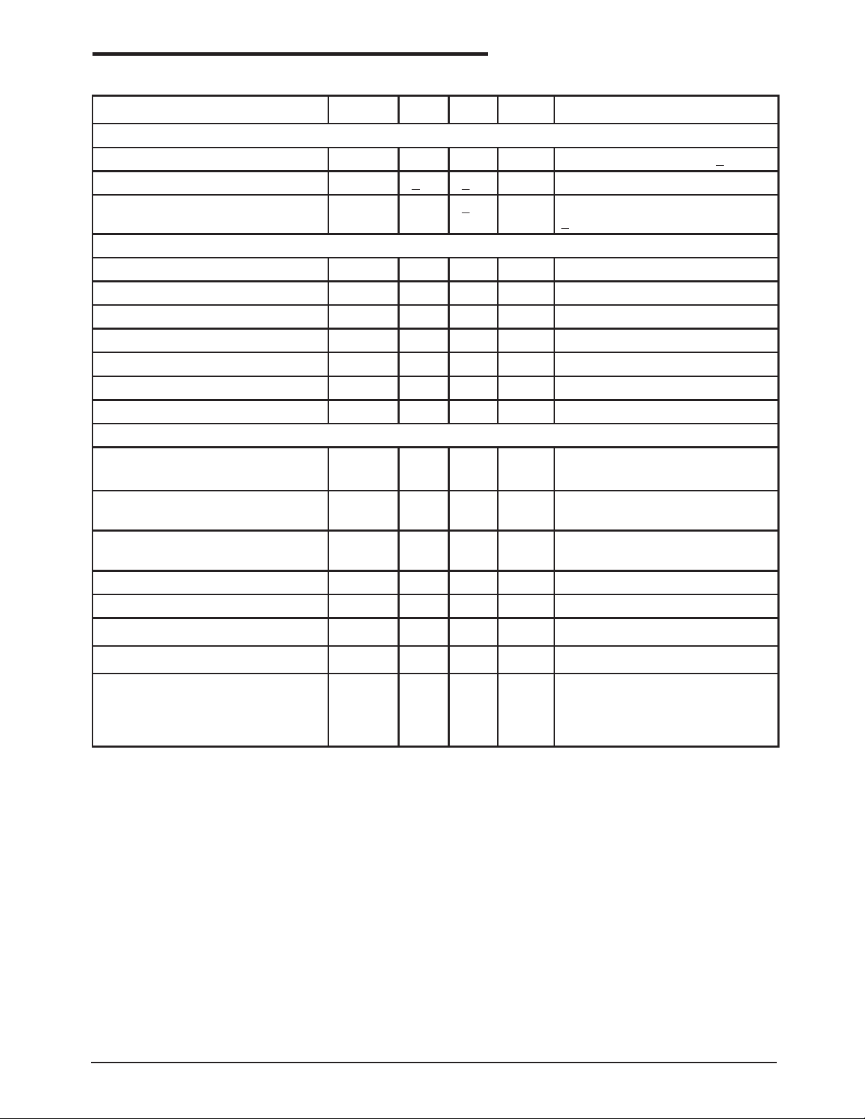
Unless otherwise noted, the following specifi cations apply for VCC = +3.0V to +5.5V with T
AMB
= T
MIN
to T
MAX
,
C1 - C4 = 0.1µF. Typical values apply at V
CC
= +3.3V or +5.0V and T
AMB
= 25°C.
ELECTRICAL CHARACTERISTICS
PARAMETER MIN. TYP. MAX. UNITS CONDITIONS
DRIVER OUTPUTS (continued)
Output Resistance 300 Ω V
CC
= V+ = V- = 0V, V
OUT
=+2V
Output Short-Circuit Current +35 +60 mA V
OUT
= 0V
Output Leakage Current +25 µA V
CC
= 0V or 3.0V to 5.5V, V
OUT
=
+12V, Drivers disabled
RECEIVER INPUTS
Input Voltage Range -15 15 V
Input Threshold LOW 0.6 1.2 V Vcc = 3.3V
Input Threshold LOW 0.8 1.5 V Vcc = 5.0V
Input Threshold HIGH 1.5 2.4 V Vcc = 3.3V
Input Threshold HIGH 1.8 2.4 V Vcc = 5.0V
Input Hysteresis 0.3 V
Input Resistance 3 5 7 kΩ
TIMING CHARACTERISTICS
Maximum Data Rate 250 kbps R
L
= 3kΩ, CL = 1000pF, one
driver active
Receiver Propagation Delay, t
PHL
0.15 µs Receiver input to Receiver
output, CL = 150pF
Receiver Propagation Delay, t
PLH
0.15 µs Receiver input to Receiver
output, C
L
= 150pF
Receiver Output Enable Time 200 ns
Receiver Output Disable Time 200 ns
Driver Skew 100 ns | t
PHL
- t
PLH
|, T
AMB
= 25°C
Receiver Skew 50 ns | t
PHL
- t
PLH
|
Transition-Region Slew Rate 30 V/µs Vcc = 3.3V, R
L
= 3kΩ,
C
L
= 1000pF, T
AMB
= 25°C,
measurements taken from -3.0V
to +3.0V or +3.0V to -3.0V
Exar Corporation 48720 Kato Road, Fremont CA, 94538 • 510-668-7017 • www.exar.com SP3222EB/SP3232EB_104_052615
3
Page 4
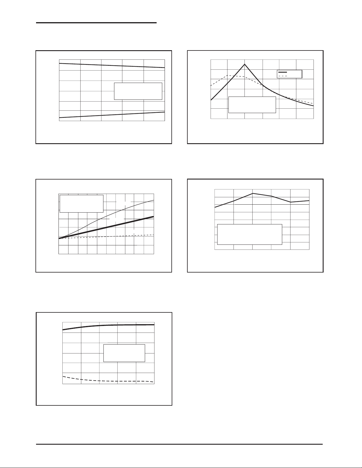
Unless otherwise noted, the following performance characteristics apply for VCC = +3.3V, 1000kbps data rate, all
drivers loaded with 3kΩ, 0.1µF charge pump capacitors, and T
AMB
= +25°C.
Figure 2. Slew Rate vs Load Capacitance
Figure 1. Transmitter Output Voltage vs Load
Capacitance
6
4
2
0
-2
-4
-6
0 1000 2000 3000 4000 5000
TxOUT +
TxOUT -
Transmitter Output
Voltage (V)
Load Capacitance (pF)
T1 at 250Kbps
T2 at 15.6Kbps
All TX loaded 3K // CLoad
Figure 3. Supply Current VS. Load Capacitance
when Transmitting Data
Figure 5. Transmitter Output Voltage vs Supply
Voltage
Figure 4. Supply Current VS. Supply Voltage
TYPICAL PERFORMANCE CHARACTERISTICS
30
25
20
15
10
5
0
0 500 1000 2000 3000 4000 5000
Slew rate (V/µs)
Load Capacitance (pF)
- Slew
+ Slew
T1 at 250Kbps
T2 at 15.6Kbps
All TX loaded 3K // CLoad
6
4
2
0
-2
-4
-6
2.7 3 3.5 4 4.5 5
Supply Voltage (V)
Transmitter Output
Voltage (V)
TxOUT -
TxOUT +
T1 at 250Kbps
T2 at 15.6Kbps
All TX loaded 3K // 1000 pF
35
30
25
20
15
10
5
0
Supply Current (mA)
Load Capacitance (pF)
0 1000 2000 3000 4000 5000
250Kbps
125Kbps
20Kbps
T1 at Full Data Rate
T2 at 1/16 Data Rate
All TX loaded 3K // CLoad
16
14
12
10
8
6
4
2
0
2.7 3 3.5 4 4.5 5
Supply Current (mA)
Supply Voltage (V)
1 Transmitter at 250Kbps
1 Transmitter at 15.6Kbps
All transmitters loaded with 3K // 1000pf
4
Exar Corporation 48720 Kato Road, Fremont CA, 94538 • 510-668-7017 • www.exar.com SP3222EB/SP3232EB_104_052615
Page 5
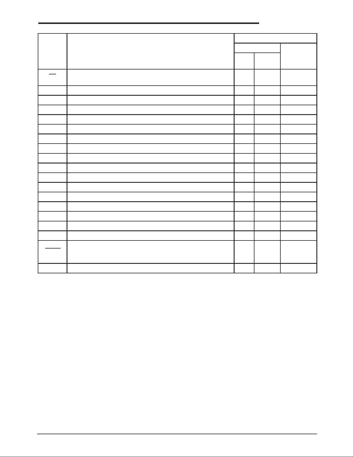
Ta ble 1. Device Pin Description
NAME FUNCTION
PIN NUMBER
SP3222EB SP3232EB
SOIC SSOP
TSSOP
EN
Receiver Enable. Apply Logic LOW for normal operation.
Apply logic HIGH to disable the receiver outputs (high-Z state)
1 1 -
C1+ Positive terminal of the voltage doubler charge-pump capacitor 2 2 1
V+ +5.5V output generated by the charge pump 3 3 2
C1- Negative terminal of the voltage doubler charge-pump capacitor 4 4 3
C2+ Positive terminal of the inverting charge-pump capacitor 5 5 4
C2- Negative terminal of the inverting charge-pump capacitor 6 6 5
V- -5.5V output generated by the charge pump 7 7 6
T
1
OUT RS-232 driver output. 15 17 14
T
2
OUT RS-232 driver output. 8 8 7
R
1
IN RS-232 receiver input 14 16 13
R
2
IN RS-232 receiver input 9 9 8
R
1
OUT TTL/CMOS receiver output 13 15 12
R
2
OUT TTL/CMOS receiver output 10 10 9
T
1
IN TTL/CMOS driver input 12 13 11
T
2
IN TTL/CMOS driver input 11 12 10
GND Ground. 16 18 15
V
CC
+3.0V to +5.5V supply voltage 17 19 16
SHDN
Shutdown Control Input. Drive HIGH for normal device operation.
Drive LOW to shutdown the drivers (high-Z output) and the onboard power supply
18 20 -
N.C. No Connect - 11, 14 -
PIN FUNCTION
Exar Corporation 48720 Kato Road, Fremont CA, 94538 • 510-668-7017 • www.exar.com SP3222EB/SP3232EB_104_052615
5
Page 6
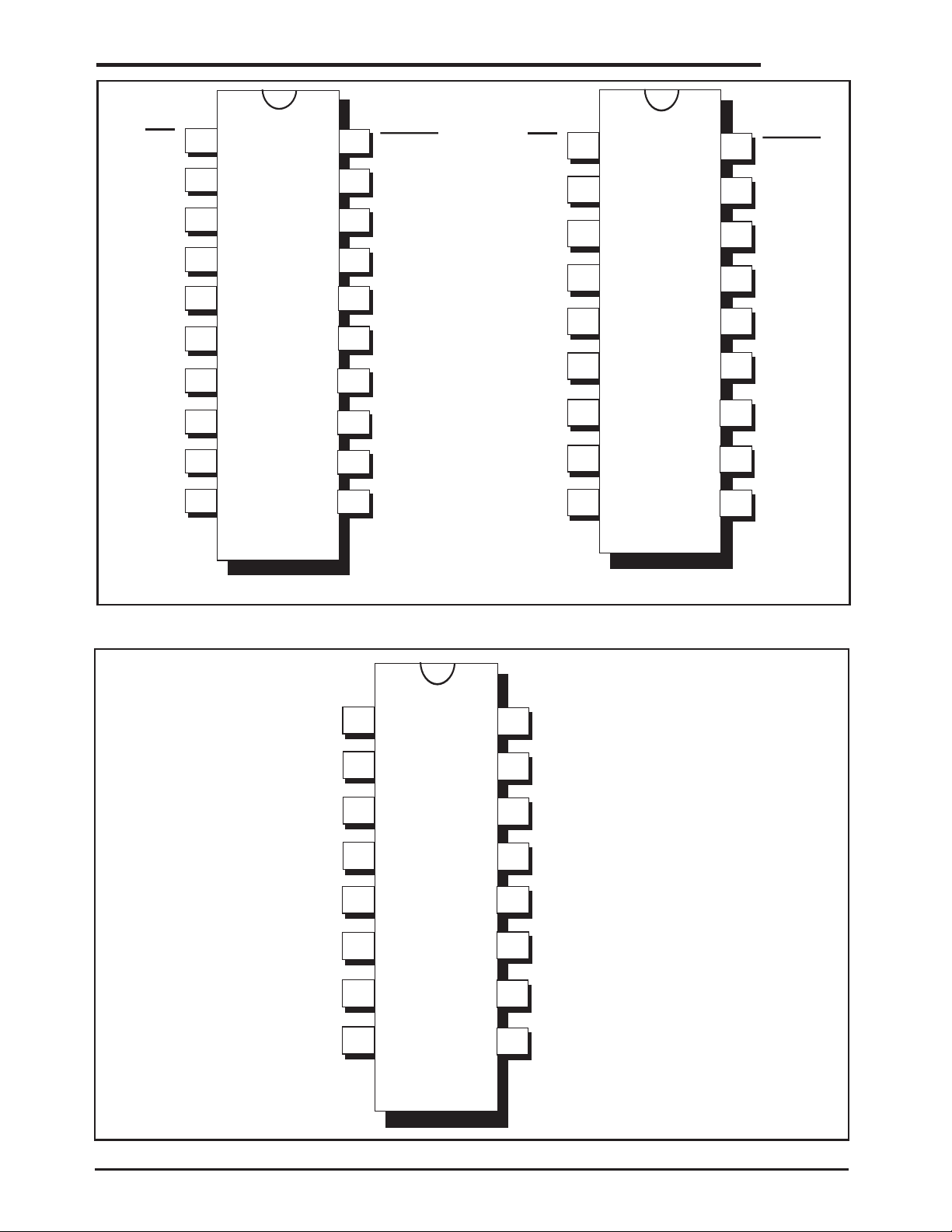
Figure 7. Pinout Confi guration for the SP3232EB
Figure 6. Pinout Confi gurations for the SP3222EB
V-
1
2
3
4
17
18
19
20
5
6
7
16
15
14
SHDN
C1+
V+
C1-
C2+
C2-
N.C.
EN
R1IN
GND
V
CC
T1OUT
N.C.
8
9
10
11
12
13
R2IN
R2OUT
SP3222EB
T2OUT
T1IN
T2IN
R1OUT
SSOP/TSSOP
V-
1
2
3
4
15
16
17
18
5
6
7
14
13
12
SHDN
C1+
V+
C1-
C2+
C2-
EN
R1IN
GND
V
CC
T1OUT
8
9
10
11
R2IN
SP3222EB
T2OUT
T2IN
T1IN
R1OUT
nSOIC
R2OUT
V-
1
2
3
4
13
14
15
16
5
6
7
12
11
10
C1+
V+
C1-
C2+
C2-
R1IN
R2IN
GND
V
CC
T1OUT
T2IN
8
9
SP3232EB
T1IN
R1OUT
R2OUT
T2OUT
PINOUT
6
Exar Corporation 48720 Kato Road, Fremont CA, 94538 • 510-668-7017 • www.exar.com SP3222EB/SP3232EB_104_052615
Page 7
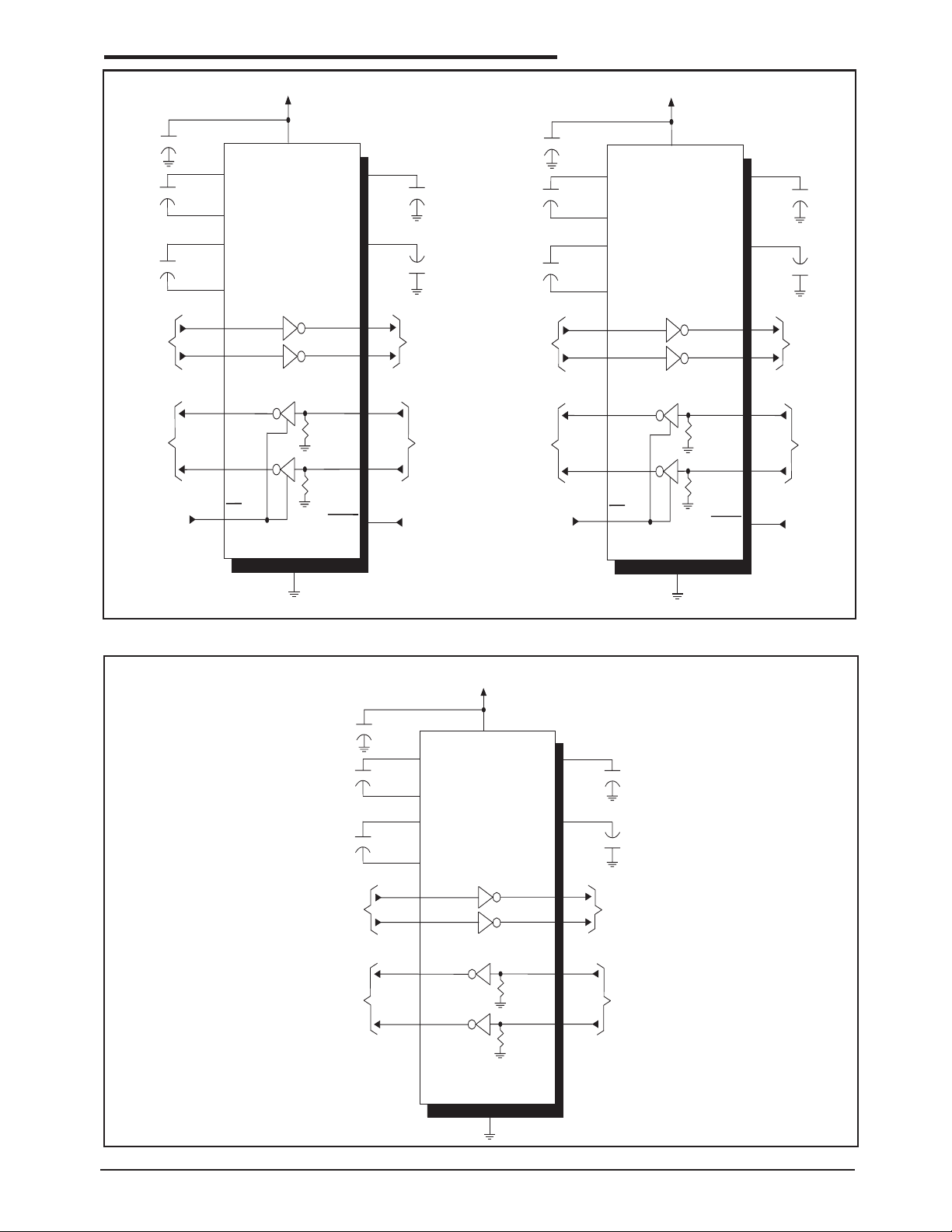
Figure 8. SP3222EB Typical Operating Circuits
SP3222EB
2
4
6
5
3
7
19
GND
T1IN
T2IN
T1OUT
T2OUT
C1+
C1-
C2+
C2-
V+
V-
VCC
13
12
0.1µF
0.1µ F
0.1µF
+
C2
C5
C1
+
+
*C3
C4
+
+
0.1µF
0.1µF
8
17
RS-232
OUTPUTS
RS-232
INPUTS
LOGIC
INPUTS
VCC
18
1
5kΩ
R1IN
R1OUT
15
9
5kΩ
R2IN
R2OUT
10
16
LOGIC
OUTPUTS
EN
20
SHDN
*can be returned to
either VCC or GND
SSOP
TSSOP
SP3222EB
2
4
6
5
3
7
17
GND
T1IN
T2IN
T1OUT
T2OUT
C1+
C1-
C2+
C2-
V+
V-
VCC
12
11
0.1µF
0.1µF
0.1µF
+
C2
C5
C1
+
+
*C3
C4
+
+
0.1µF
0.1µF
8
15
RS-232
OUTPUTS
RS-232
INPUTS
LOGIC
INPUTS
VCC
16
1
5kΩ
R1IN
R1OUT
13
9
5kΩ
R2IN
R2OUT
10
14
LOGIC
OUTPUTS
EN
18
SHDN
*can be returned to
either VCC or GND
nSOIC
Figure 9. SP3232EB Typical Operating Circuit
SP3232EB
1
3
5
4
2
6
16
GND
T1IN
T2IN
T1OUT
T2OUT
C1+
C1-
C2+
C2-
V+
V-
V
CC
11
10
0.1µF
+
C2
C5
C1
+
+
*C3
C4
+
+
14
7
RS-232
OUTPUTS
RS-232
INPUTS
LOGIC
INPUTS
V
CC
15
5kΩ
R1IN
R1OUT
12
13
5kΩ
R2IN
R2OUT
9
8
LOGIC
OUTPUTS
*can be returned to
either V
CC or GND
0.1µF
0.1µF
0.1µF
0.1µF
TYPICAL OPERATING CIRCUITS
Exar Corporation 48720 Kato Road, Fremont CA, 94538 • 510-668-7017 • www.exar.com SP3222EB/SP3232EB_104_052615
7
Page 8
The SP3222EB/SP3232EB transceivers
meet the EIA/TIA-232 and ITU-T V.28/V.24
communication protocols and can be implemented in battery-powered, portable, or
hand-held applications such as notebook
or palmtop computers. The SP3222EB/
SP3232EB devices feature Exar's propri-
etary on-board charge pump circuitry that
generates ±5.5V for RS-232 voltage levels
from a single +3.0V to +5.5V power supply.
This series is ideal for +3.3V-only systems,
mixed +3.3V to +5.5V systems, or +5.0V-only
systems that require true RS-232 performance. The SP3222EB/SP3232EB d e vices
can operate at a data rate of 250kbps when
fully loaded.
The SP3222EB and SP3232EB are 2-
driver/2- receiver devices ideal for portable
or hand-held applications. The SP3222EB
features a 1µA s h utdown mode that reduces
power consumption and extends battery life
in portable systems. Its receivers remain
active in shutdown mode, allowing external
devices such as modems to be monitored
using only 1µA supply current.
THEORY OF OPERATION
The SP3222EB/SP3232EB series is made
up of three basic circuit blocks:
1. Drivers
2. Receivers
3. The Exar proprietary charge pump
Drivers
The drivers are inverting level transmitters
that convert TTL or CMOS logic levels to
+5.0V EIA/TIA-232 levels with an inverted
sense relative to the input logic levels.
Typically, the RS-232 output voltage swing
is +5.4V with no load and +5V minimum fully
loaded. The driver outputs are protected
against infi nite short-circuits to ground without degradation in reliability. Driver outputs
will meet EIA/TIA-562 levels of +/-3.7V with
supply voltages as low as 2.7V.
The drivers can guarantee a data rate of
250kbps fully loaded with 3kΩ in parallel
with 1000pF, ensuring compatability with
PC-to-PC communication software.
The slew rate of the driver is internally limited
to a maximum of 30V/µs in order to meet the
EIA standards (EIA RS-232D 2.1.7, Paragraph 5). The transition of the loaded output
from HIGH to LOW also meet the monotonicity requirements of the standard.
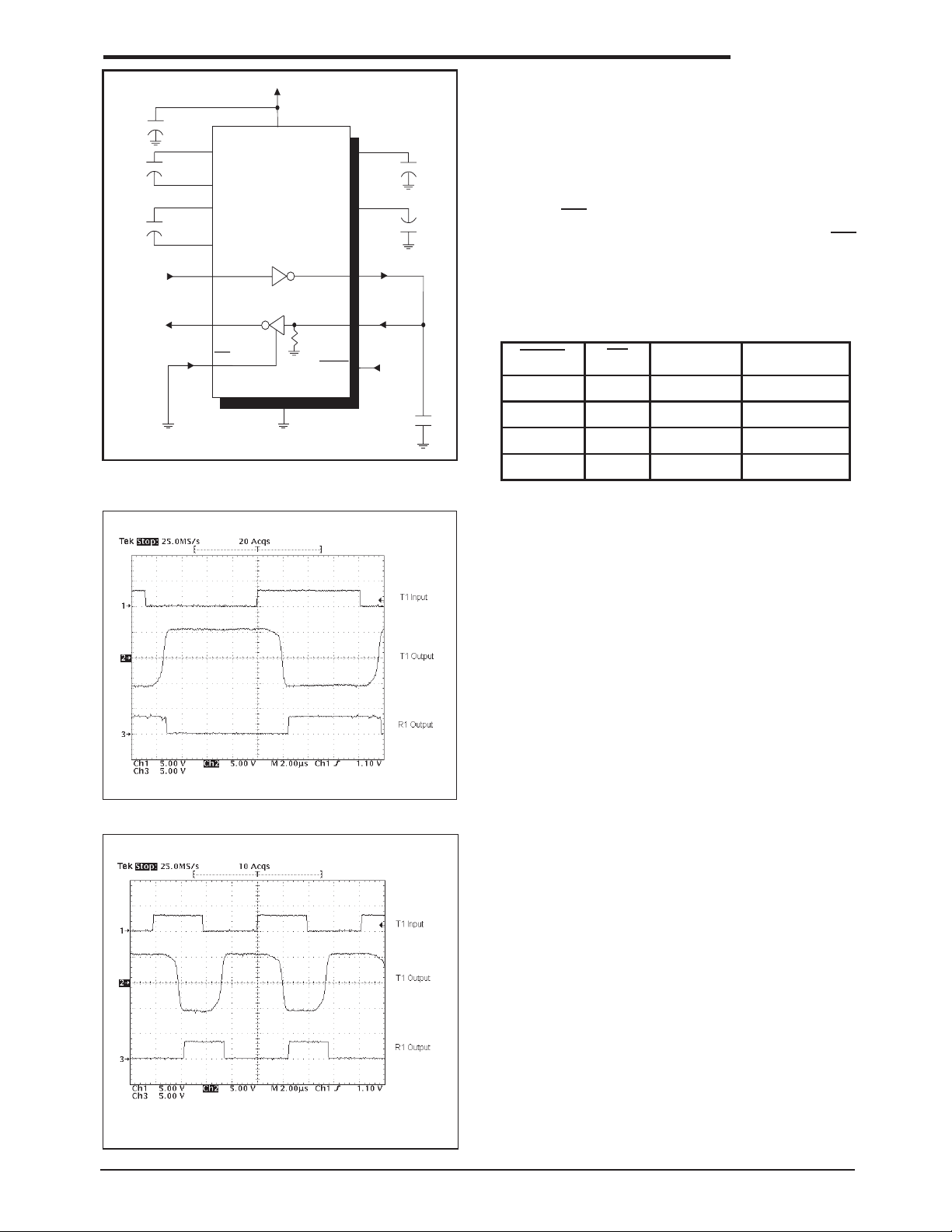
Figure 10 shows a loopback test circuit
used to test the RS-232 Drivers. Figure
11 shows the test results of the loopback
circuit with all drivers active at 120kbps
with RS-232 loads in parallel with a
1000pF capacitor. Figure 12 shows the
test results where one driver was active
at 250kbps and all drivers loaded with an
RS-232 receiver in parallel with 1000pF
capacitors. A solid RS-232 data transmission rate of 250kbps provides compatibility
with many designs in personal computer
peripherals and LAN applications.
The SP3222EB driver's output stages are
turned off (tri-state) when the device is in
shutdown mode. When the power is off, the
SP3222EB device permits the outputs to be
driven up to +/-12V. The driver's inputs do
not have pull-up resistors. Designers should
connect unused inputs to Vcc or GND.
In the shutdown mode, the supply current
falls to less than 1µA, where SHDN = LOW.
When the SP3222EB device is shut down,
the device's driver outputs are disabled (tristated) and the charge pumps are turned off
with V+ pulled down to Vcc and V- pulled to
GND. The time required to exit shutdown is
typically 100µs. Connect SHDN to Vcc if the
shutdown mode is not used.
DESCRIPTION
8
Exar Corporation 48720 Kato Road, Fremont CA, 94538 • 510-668-7017 • www.exar.com SP3222EB/SP3232EB_104_052615
Page 9
Receivers
The Receivers convert EIA/TIA-232 levels
to TTL or CMOS logic output levels. The
SP3222EB receivers have an inverting
tri-state output. These receiver outputs
(RxOUT) are tri-stated when the enable
control EN = HIGH. In the shutdown mode,
the receivers can be active or inactive. EN
has no effect on TxOUT. The truth table logic
of the SP3222EB d r iver and receiver outputs
can be found in Table 2.
Since receiver input is usually from a transmission line where long cable lengths and
system interference can degrade the signal,
the inputs have a typical hysteresis margin
of 300mV. This ensures that the receiver
is virtually immune to noisy transmission
lines. Should an input be left unconnected,
an internal 5kΩ pulldown resistor to ground
will commit the output of the receiver to a
HIGH state.
Ta ble 2. SP3222EB Truth Table Logic for Shutdown
and Enable Control
Figure 10. SP3222EB/SP3232EB Driver Loopback
Te st Circuit
Charge Pump
The charge pump is an Exar-patended
design (U.S. 5,306,954) and uses a unique
approach compared to older less-effi cient
designs. The charge pump still requires four
external capacitors, but uses a four-phase
voltage shifting technique to attain symmetrical 5.5V power supplies. The internal
power supply consists of a regulated dual
charge pump that provides output voltages
of +/-5.5V regardless of the input voltage
(Vcc) over the +3.0V to +5.5V range.
Figure 12. Loopback Test results at 250kbps
Figure 11. Loopback Te st results at 120kbps
SP3222EB
SP3232EB
GND
TxIN
TxOUT
C1+
C1-
C2+
C2-
V+
V-
V
CC
0.1µF
0.1µF
0.1µF
+
C2
C5
C1
+
+
C3
C4
+
+
0.1µF
0.1µF
LOGIC
INPUTS
V
CC
5kΩ
RxIN
RxOUT
LOGIC
OUTPUTS
EN*
*SHDN
1000pF
V
CC
* SP3222EB only
SHDN EN TxOUT RxOUT
0 0 Tri-state Active
0 1 Tri-state Tri-state
1 0 Active Active
1 1 Active Tri-state
DESCRIPTION
Exar Corporation 48720 Kato Road, Fremont CA, 94538 • 510-668-7017 • www.exar.com SP3222EB/SP3232EB_104_052615
9
Page 10

In most circumstances, decoupling the power
supply can be achieved adequately using
a 0.1µF bypass capacitor at C5 (refer to
fi g ures 8 and 9)
In applications that are sensitive to powersupply noise, decouple Vcc to ground with a
capacitor of the same value as charge-pump
capacitor C1. Physically connect bypass
capcitors as close to the IC as possible.
The charge pump operates in a discontinuous mode using an internal oscillator. If the
output voltages are less than a magnitude
of 5.5V, the charge pump is enabled. If the
output voltages exceed a magnitude of 5.5V,
the charge pump is disabled. This oscillator
controls the four phases of the voltage shifting. A description of each phase follows.
Phase 1
— V
SS
charge storage — During this phase
of the clock cycle, the positive side of capacitors C
1
and C2 are initially charged to VCC.
C
l
+
is then switched to GND and the charge
in C
1
–
is transferred to C
2
–
. Since C
2
+
is con-
nected to V
CC
, the voltage potential across
capacitor C2 is now 2 times VCC.
Phase 2
— VSS transfer — Phase two of the clock
connects the negative terminal of C2 t o t h e V
SS
storage capacitor and the positive terminal of
C2 to GND. This transfers a negative generated voltage to C3. This generated voltage is
regulated to a minimum voltage of -5.5V.
Simultaneous with the transfer of the voltage to C
3
, the positive side of capacitor C1
is switched to V
CC
and the negative side is
connected to GND.
Phase 3
— V
DD
charge storage — The third phase of
the clock is identical to the fi rst phase — the
charge transferred in C
1
produces –VCC in
the negative terminal of C1, which is applied
to the negative side of capacitor C2. Since
C
2
+
is at VCC, the voltage potential across C2
is 2 times VCC.
Phase 4
— VDD transfer — The fourth phase of
the clock connects the negative terminal
of C
2
to GND, and transfers this positive
generated voltage across C2 to C4, the
VDD storage capacitor. This voltage is
regulated to +5.5V. At this voltage, the internal oscillator is disabled. Simultaneous
with the transfer of the voltage to C
4
, the
positive side of capacitor C1 is switched
to VCC and the negative side is connected to GND, allowing the charge
pump cycle to begin again. The charge
pump cycle will continue as long as the
operational conditions for the internal
oscillator are present.
Since both V+ and V– are separately generated from VCC, in a no–load condition V+
and V
–
will be symmetrical. Older charge
pump approaches that generate V
–
from
V+ will show a decrease in the magnitude
of V– compared to V+ due to the inherent
ineffi ciencies in the design.
The clock rate for the charge pump typically
operates at greater than 250kHz. The external capacitors can be as low as 0.1µF with
a 16V breakdown voltage rating.
DESCRIPTION
10
Exar Corporation 48720 Kato Road, Fremont CA, 94538 • 510-668-7017 • www.exar.com SP3222EB/SP3232EB_104_052615
Page 11
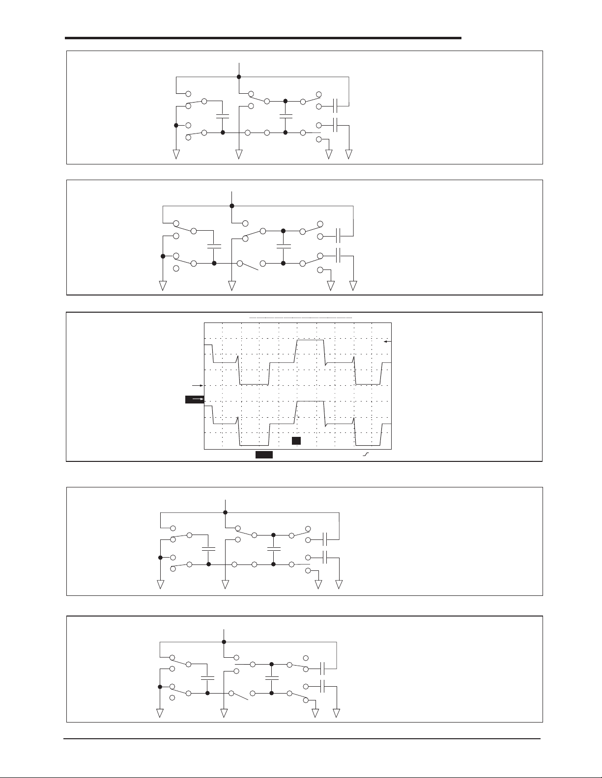
Figure 14. Charge Pump — Phase 2
VCC = +5V
V
SS
Storage Capacitor
V
DD
Storage Capacitor
C
1
C
2
C
3
C
4
+
+
+ +
–
–
–
–
-5.5V
VCC = +5V
–5V
–5V
+5V
V
SS
Storage Capacitor
VDD Storage Capacitor
C
1
C
2
C
3
C
4
+
+
+ +
–
–
–
–
Figure 13. Charge Pump — Phase 1
Figure 16. Charge Pump — Phase 3
VCC = +5V
–5V
–5V
+5V
V
SS
Storage Capacitor
V
DD
Storage Capacitor
C
1
C
2
C
3
C
4
+
+
+ +
–
–
––
Figure 17. Charge Pump — Phase 4
VCC = +5V
V
SS
Storage Capacitor
V
DD
Storage Capacitor
C
1
C
2
C
3
C
4
+
+
+ +
–
–
–
–
+5.5V
Figure 15. Charge Pump Waveforms
Ch1 2.00V Ch2 2.00V M 1.00ms Ch1 5.48V
2
1
T
T[]
T
+6V
a) C
2+
b) C2-
GND
GND
-6V
DESCRIPTION
Exar Corporation 48720 Kato Road, Fremont CA, 94538 • 510-668-7017 • www.exar.com SP3222EB/SP3232EB_104_052615
11
Page 12
ESD TOLERANCE
The SP3222EB/SP3232EB series incorporates ruggedized ESD cells on all driver
output and receiver input pins. The ESD
structure is improved over our previous
family for more rugged applications and
environments sensitive to electro-static
discharges and associated transients. The
improved ESD tolerance is at least +15kV
without damage nor latch-up.
There are different methods of ESD testing
applied:
a) MIL-STD-883, Method 3015.7
b) IEC61000-4-2 Air-Discharge
c) IEC61000-4-2 Direct Contact
The Human Body Model has been the
generally accepted ESD testing method
for semi-conductors. This method is also
specifi ed in MIL-STD-883, Method 3015.7
for ESD testing. The premise of this ESD test
is to simulate the human body’s potential to
store electro-static energy and discharge it
to an integrated circuit. The simulation is
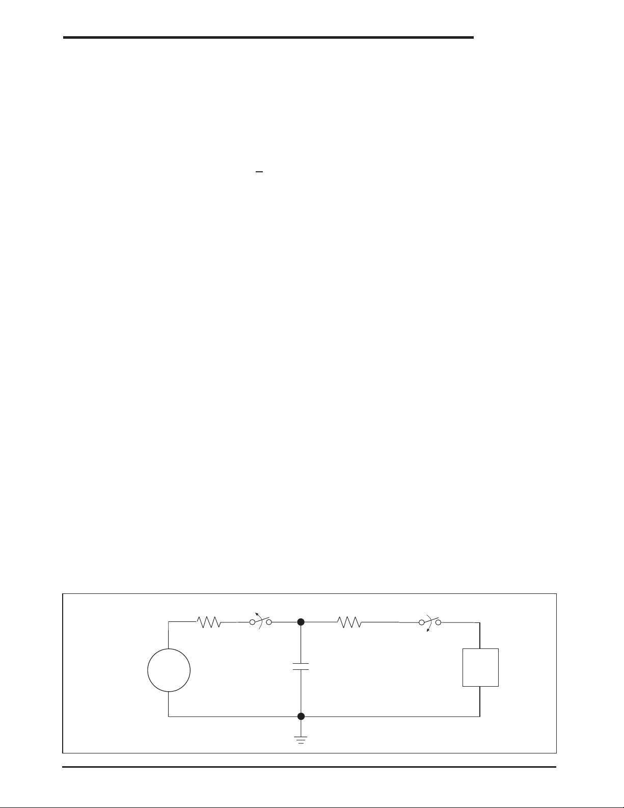
performed by using a test model as shown
in Figure 18. This method will test the IC’s
capability to withstand an ESD transient
during normal handling such as in manufacturing areas where the ICs tend to be
handled frequently.
The IEC-61000-4-2, formerly IEC801-2, is
generally used for testing ESD on equipment
and systems. For system manufacturers,
they must guarantee a certain amount of ESD
protection since the system itself is exposed
to the outside environment and human presence. The premise with IEC61000-4-2 is that
the system is required to withstand an amount
of static electricity when ESD is applied to
points and surfaces of the equipment that
are accessible to personnel during normal
usage. The transceiver IC receives most
of the ESD current when the ESD source is
applied to the connector pins. The test circuit
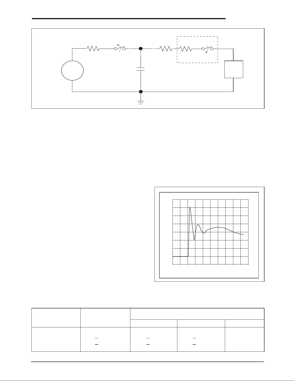
for IEC61000-4-2 is shown on Figure 19.
There are two methods within IEC61000-4-2,
the Air Discharge method and the Contact
Discharge method.
With the Air Discharge Method, an ESD
voltage is applied to the equipment under
test (EUT) through air. This simulates an
electrically charged person ready to connect
a cable onto the rear of the system only to
fi n d an unpleasant zap just before the person
touches the back panel. The high energy
potential on the person discharges through
an arcing path to the rear panel of the system
before he or she even touches the system.
This energy, whether discharged directly or
through air, is predominantly a function of the
discharge current rather than the discharge
voltage. Variables with an air discharge such
as approach speed of the object carrying the
ESD potential to the system and humidity
will tend to change the discharge current.
For example, the rise time of the discharge
current varies with the approach speed.
The Contact Discharge Method applies the
ESD current directly to the EUT. This method
was devised to reduce the unpredictability
of the ESD arc. The discharge current rise
time is constant since the energy is directly
transferred without the air-gap arc. In situations such as hand held systems, the ESD
charge can be directly discharged to the
Figure 18. ESD Test Circuit for Human Body Model
R
C
Device
Under
Test
DC Power
Source
C
S
R
S
SW1
SW2
DESCRIPTION
12
Exar Corporation 48720 Kato Road, Fremont CA, 94538 • 510-668-7017 • www.exar.com SP3222EB/SP3232EB_104_052615
Page 13
DEVICE PIN HUMAN BODY IEC61000-4-2
TESTED MODEL Air Discharge Direct Contact Level
Driver Outputs +15kV +15kV +8kV 4
Receiver Inputs +15kV +15kV +8kV 4
equipment from a person already holding
the equipment. The current is transferred
on to the keypad or the serial port of the
equipment directly and then travels through
the PCB and fi nally to the IC.
The circuit models in Figures 18 and 19 represent the typical ESD testing circuit used for
all three methods. The C
S
i s initially charged
with the DC power supply when the fi rst
switch (SW1) is on. Now that the capacitor
is charged, the second switch (SW2) is on
while SW1 switches off. The voltage stored
in the capacitor is then applied through R
S
,
the current limiting resistor, onto the device
under test (DUT). In ESD tests, the SW2
switch is pulsed so that the device under
test receives a duration of voltage.
For the Human Body Model, the current
limiting resistor (R
S
) and the source capacitor
(CS) are 1.5kΩ an 100pF, respectively. For
IEC-61000-4-2, the current limiting resistor
(R
S
) and the source capacitor (CS) are 330Ω
an 150pF, respectively.
Figure 20. ESD Test Waveform for IEC61000-4-2
Figure 19. ESD Test Circuit for IEC61000-4-2
Ta ble 3. Transceiver ESD Tolerance Levels
R
S
and
R
V
add up to 330Ω for IEC1000-4-2.
R
C
Device
Under
Test
DC Power
Source
C
S
R
S
SW1
SW2
R
V
Contact-Discharge Model
t = 0ns t = 30ns
0A
15A
30A
I →
t →
The higher CS value and lower RS value in
the IEC61000-4-2 model are more stringent
than the Human Body Model. The larger
storage capacitor injects a higher voltage
to the test point when SW2 is switched on.
The lower current limiting resistor increases
the current charge onto the test point.
DESCRIPTION
Exar Corporation 48720 Kato Road, Fremont CA, 94538 • 510-668-7017 • www.exar.com SP3222EB/SP3232EB_104_052615
13
Page 14
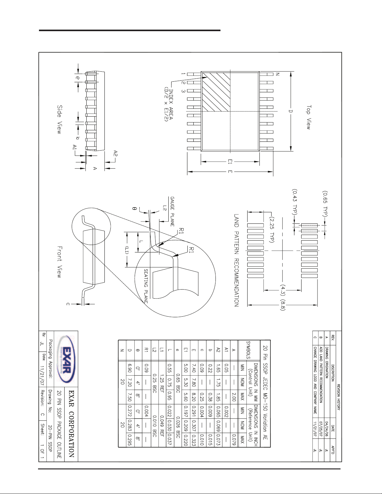
PACKAGE: 20 PIN SSOP
14
Exar Corporation 48720 Kato Road, Fremont CA, 94538 • 510-668-7017 • www.exar.com SP3222EB/SP3232EB_104_052615
Page 15
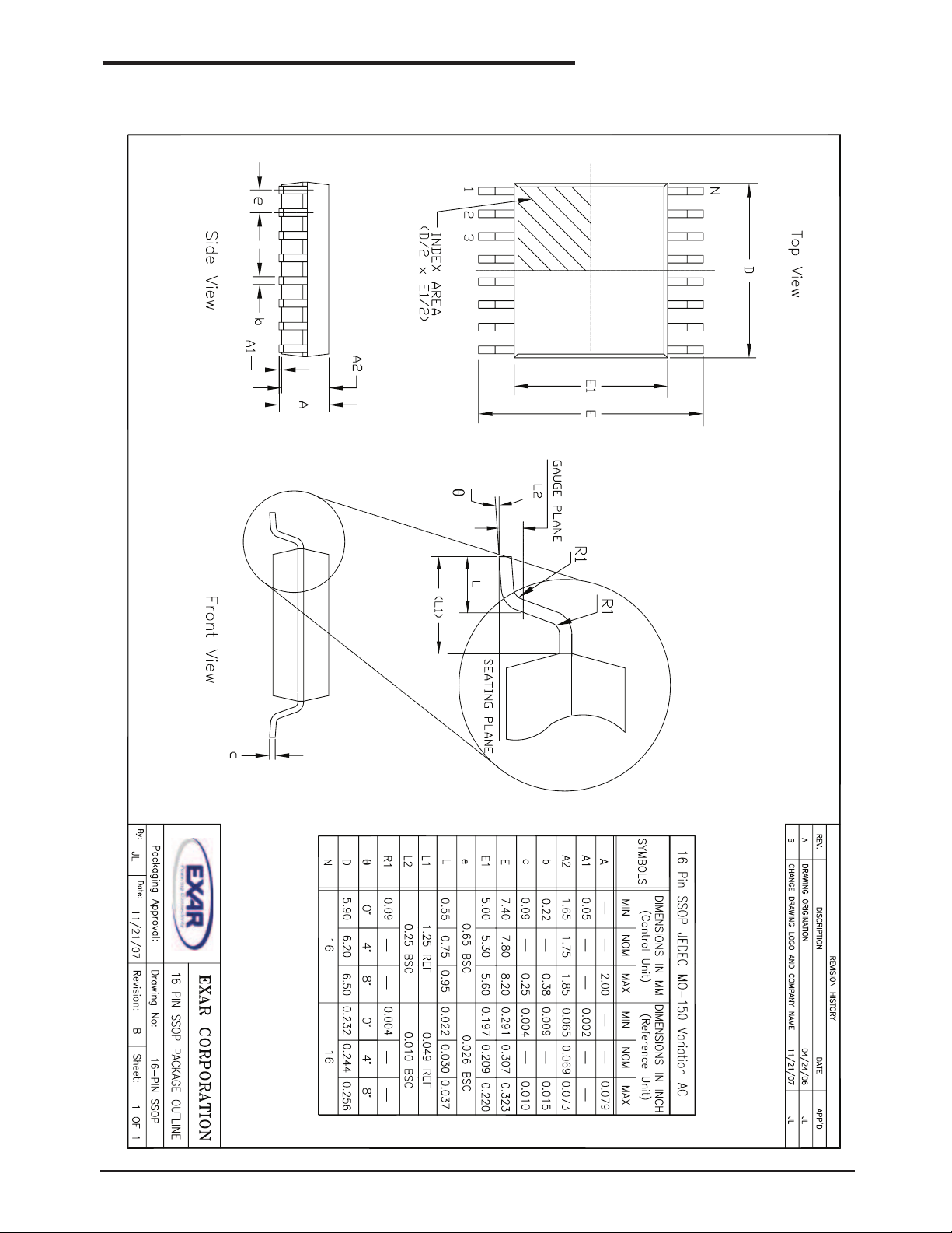
PACKAGE: 16 PIN SSOP
Exar Corporation 48720 Kato Road, Fremont CA, 94538 • 510-668-7017 • www.exar.com SP3222EB/SP3232EB_104_052615
15
Page 16
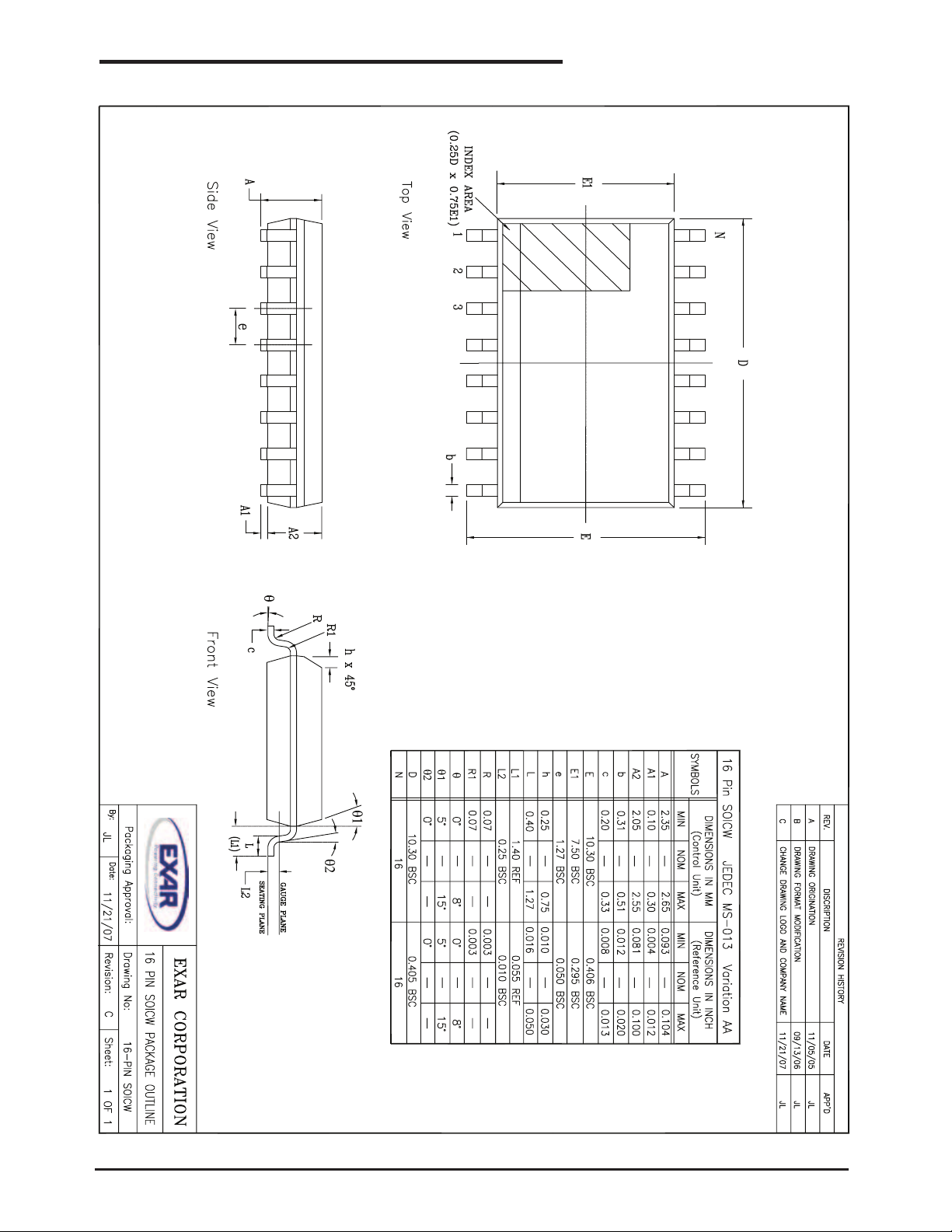
PACKAGE: 16 PIN WSOIC
16
Exar Corporation 48720 Kato Road, Fremont CA, 94538 • 510-668-7017 • www.exar.com SP3222EB/SP3232EB_104_052615
Page 17
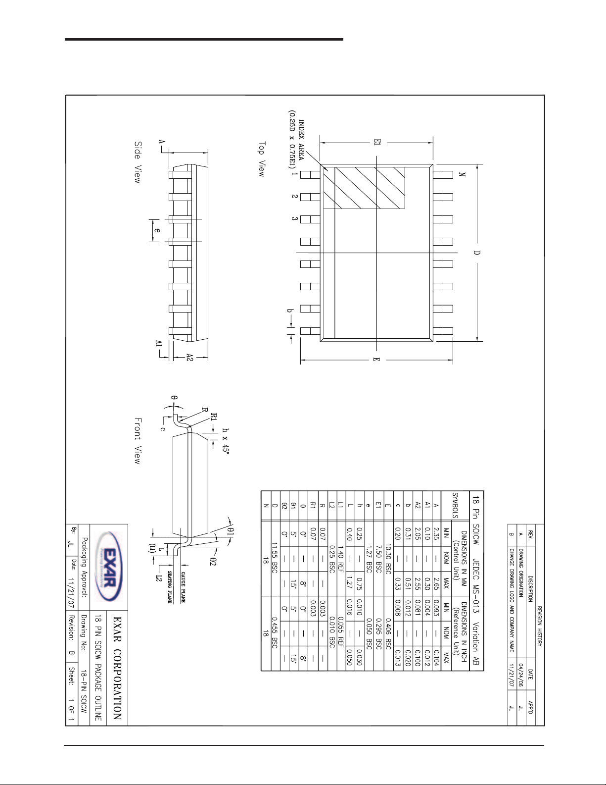
PACKAGE: 18 PIN WSOIC
Exar Corporation 48720 Kato Road, Fremont CA, 94538 • 510-668-7017 • www.exar.com SP3222EB/SP3232EB_104_052615
17
Page 18
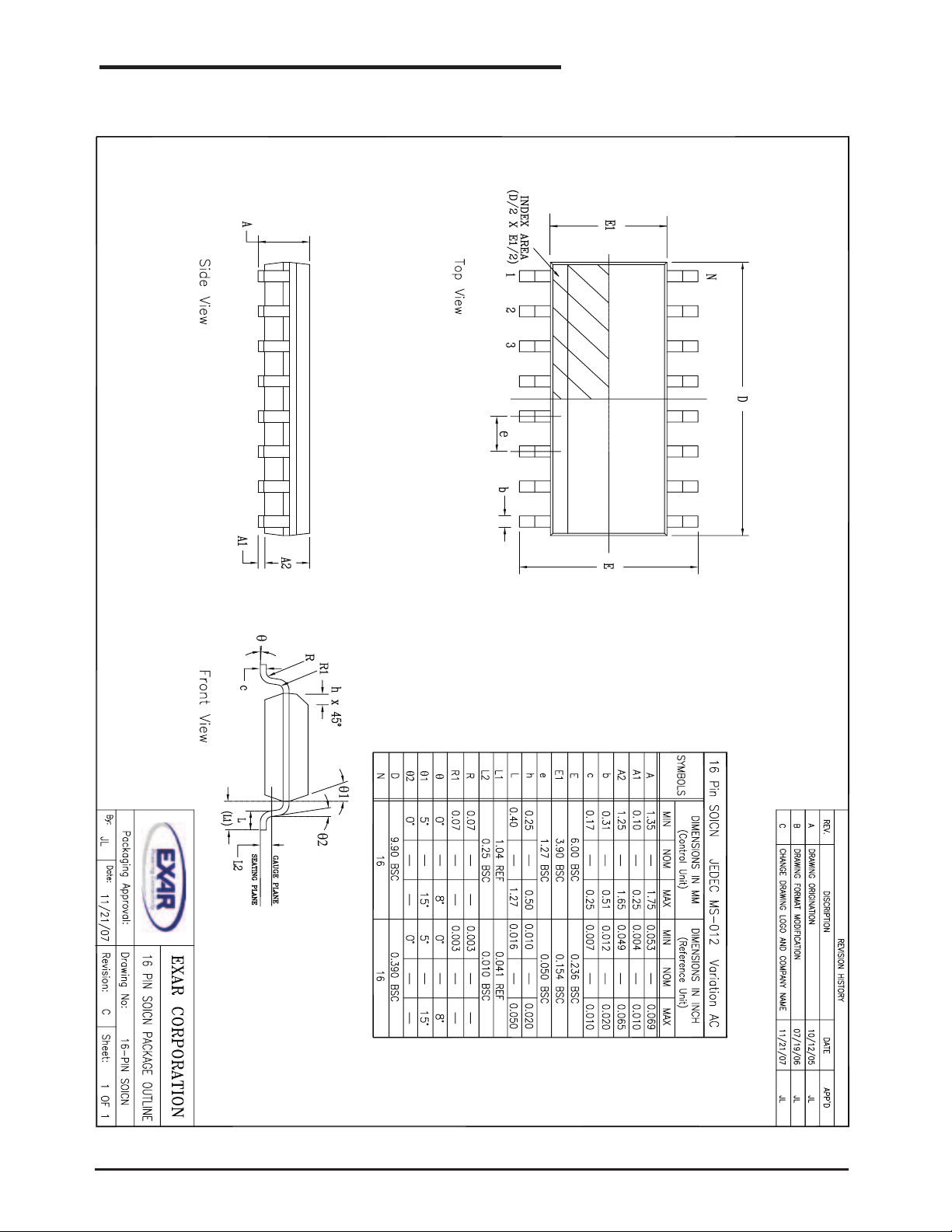
PACKAGE: 16 PIN nSOIC
18
Exar Corporation 48720 Kato Road, Fremont CA, 94538 • 510-668-7017 • www.exar.com SP3222EB/SP3232EB_104_052615
Page 19
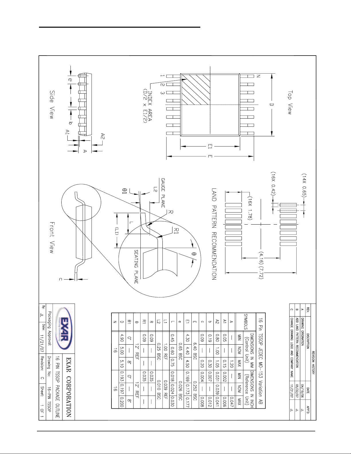
PACKAGE: 16 PIN TSSOP
Exar Corporation 48720 Kato Road, Fremont CA, 94538 • 510-668-7017 • www.exar.com SP3222EB/SP3232EB_104_052615
19
Page 20
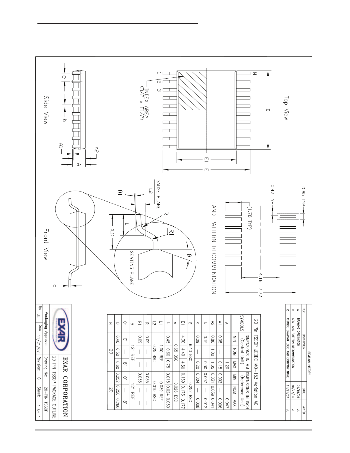
PACKAGE: 20 PIN TSSOP
20
Exar Corporation 48720 Kato Road, Fremont CA, 94538 • 510-668-7017 • www.exar.com SP3222EB/SP3232EB_104_052615
Page 21
ORDERING INFORMATION
Note: "/TR" is for tape and Reel option. "-L" is for lead free packaging
Part Number Tem p. Range Package
SP3222EBCA-L 0°C to +70°C 20 Pin SSOP
SP3222EBCA-L/TR 0°C to +70°C 20 Pin SSOP
SP3222EBCT-L 0°C to +70°C 18 Pin WSOIC
SP3222EBCT-L/TR 0°C to +70°C 18 Pin WSOIC
SP3222EBCY-L 0°C to +70°C 20 Pin TSSOP
SP3222EBCY-L/TR 0°C to +70°C 20 Pin TSSOP
SP3222EBEA-L -40°C to +85°C 20 Pin SSOP
SP3222EBEA-L/TR -40°C to +85°C 20 Pin SSOP
SP3222EBET-L -40°C to +85°C 18 Pin WSOIC
SP3222EBET-L/TR -40°C to +85°C 18 Pin WSOIC
SP3222EBEY-L -40°C to +85°C 20 Pin TSSOP
SP3222EBEY-L/TR -40°C to +85°C 20 Pin TSSOP
Part Number Tem p. Range Package
SP3232EBCA-L 0°C to +70°C 16 Pin SSOP
SP3232EBCA-L/TR 0°C to +70°C 16 Pin SSOP
SP3232EBCN-L 0°C to +70°C 16 Pin NSOIC
SP3232EBCN-L/TR 0°C to +70°C 16 Pin NSOIC
SP3232EBCT-L 0°C to +70°C 16 Pin WSOIC
SP3232EBCT-L/TR 0°C to +70°C 16 Pin WSOIC
SP3232EBCY-L 0°C to +70°C 16 Pin TSSOP
SP3232EBCY-L/TR 0°C to +70°C 16 Pin TSSOP
SP3232EBEA-L -40°C to +85°C 16 Pin SSOP
SP3232EBEA-L/TR -40°C to +85°C 16 Pin SSOP
SP3232EBEN-L -40°C to +85°C 16 Pin NSOIC
SP3232EBEN-L/TR -40°C to +85°C 16 Pin NSOIC
SP3232EBET-L -40°C to +85°C 16 Pin WSOIC
SP3232EBET-L/TR -40°C to +85°C 16 Pin WSOIC
SP3232EBEY-L -40°C to +85°C 16 Pin TSSOP
SP3232EBEY-L/TR -40°C to +85°C 16 Pin TSSOP
Exar Corporation 48720 Kato Road, Fremont CA, 94538 • 510-668-7017 • www.exar.com SP3222EB/SP3232EB_104_052615
21
Page 22
REVISION HISTORY
Notice
EXAR Corporation reserves the right to make changes to any products contained in this publication in order to improve design, performance or reliability. EXAR Corporation assumes no representation that the circuits are free of patent infringement. Charts and schedules contained herein are
only for illustration purposes and may vary depending upon a user's specifi c application. While the information in this publication has been carefully
checked; no responsibility, however, is assumed for inaccuracies.
EXAR Corporation does not recommend the use of any of its products in life support applications where the failure or malfunction of the product can
reasonably be expected to cause failure of the life support system or to signifi cantly affect its safety or effectiveness. Products are not authorized for
use in such applications unless EXAR Corporation receives, in writting, assurances to its satisfaction that: (a) the risk of injury or damage has been
minimized ; (b) the user assumes all such risks; (c) potential liability of EXAR Corporation is adequately protected under the circumstances.
Copyright 2015 EXAR Corporation
Datasheet May 2015
Send your serial transceiver technical inquiry with technical details to: [email protected]
Reproduction, in part or whole, without the prior written consent of EXAR Corporation is prohibited.
DATE REVISION DESCRIPTION
11/02/05 -- Legacy Sipex Datasheet
09/09/09 1.0.0 Convert to Exar Format, Update ordering information and
change revision to 1.0.0.
06/07/11 1.0.1 Remove obsolete devices per PDN 110510-01 and change
ESD rating to IEC-61000-4-2.
03/14/13 1.0.2 Correct type error to RX input voltage range and TX transi-
tion region slew rate condition.
8/14/14 1.0.3 Add Max Junction temperature and package thermal infor-
mation.
5/28/15 1.0.4 Update Apps Max Rating for RxIN input voltage to +/-23V,
update logo. ECN #1529-04
22
Exar Corporation 48720 Kato Road, Fremont CA, 94538 • 510-668-7017 • www.exar.com SP3222EB/SP3232EB_104_052615
 Loading...