

Page 1
2
1
3
4
5
6
7 8
9
10
11
12
13
14
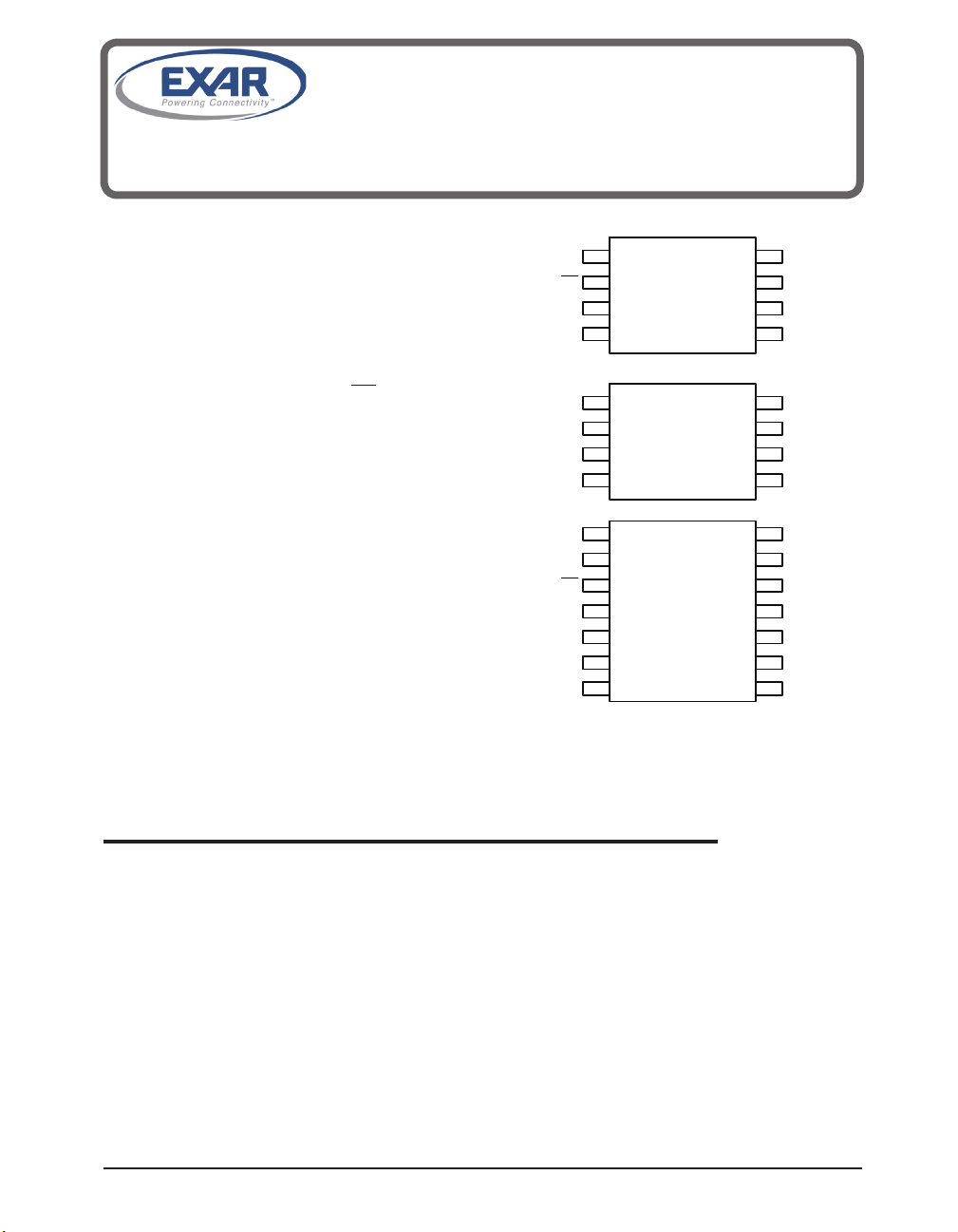
14 PIN NSOIC
Full Duplex
SP3070E
SP3073E
SP3076E
2
1
3
4 5
6
7
8
8 PIN NSOIC
Full Duplex
SP3071E
SP3074E
SP3077E
2
1
3
4 5
6
7
8
8 PIN NSOIC
Half Duplex
SP3072E
SP3075E
SP3078E
RO
RE
DE
DI GND
A
B
Vcc
Vcc
RO
DI
GND
A
B
Z
Y
DI
NC
RO
RE
DE
GND
GND NC
Y
Z
B
A
NC
Vcc
SP3070E - SP3078E Family
±15kV ESD-Protected, 3.3V, 1/8 Load, Failsafe
RS-485/RS422 Transceivers
FEATURES
■ ±15kV ESD protection for RS485 pins
■ 3.3V low-power operation
■ Advanced Receiver-failsafe protection for
open, shorted or terminated lines
■ Up to 256 Transceivers may share Bus
■ Very low load for 8x greater fanout
■ Hot Swap glitch protection RE and DE
■ Thermal shutdown protects against driver
contention
■ Available in three industry standard footprints
■ SP3070E, 3073 and 3076 in Full-Duplex (14 pin)
■ SP3071E, 3074 and 3077 in Full-Duplex (8 pin)
■ SP3072E, 3075 and 3078 in Half-Duplex (8 pin)
■ Three applications-optimized speed grades
■ SP3070E-72E: 250kbps slew-limited
■ SP3073E-75E: 500kbps slew-limited
■ SP3076E-78E: 16Mbps high speed
■ Small form factor SO-narrow packages
■ Industrial (-40 to +85ºC) and Extended
(-40 to +125ºC) temperature grades
Now Available in Lead Free Packaging
APPLICATIONS
■ Industrial Control, Utility Meters Building Automation, Instrumentation, Point of Sale
The SP3070E-3078E differential line transceivers are suitable for bidirectional communication
on balanced multipoint bus transmission lines and comply with both RS485 and RS422 EIA
Standards. Each device consists of a differential driver and differential receiver. All devices
operate from a 3.3V power supply.
High receiver input impedance allows a large number of transceivers to share a common
data bus while maintaining signal margin and without excessive loading or use of expensive
repeaters. The high impedance driver output is maintained over the entire common-mode
voltage range from -7 to +12V. Receivers will failsafe to logic 1 output when inputs are open,
shorted or terminated. Drivers include built-in short-circuit protection and a thermal-overload
shutdown to protect against excessive power dissipation from bus contention or cable faults.
All RS485 receiver inputs and driver outputs are ESD protected up to ±15kV (Air-Gap and
Human Body Model) and up to ±8kV Contact discharge (IEC 61000-4-2). The SP3070ESP3078E devices may not achieve optimal transmit performance if the connected receiver
includes a biasing network to 5.0V without a termination resistor. Please see Exar Application
Note ANI#21 for further details.
Exar Corporation 48720 Kato Road, Fremont CA, 94538 • 510-668-7017 • www.exar.com SP3070E-SP3078E_102_120210
DESCRIPTION
1
Page 2
DEVICE ARCHITECTURE AND BLOCK DIAGRAMS
VCC
D
R
NC
A
B
Z
Y
R
NC
NC
DE
REB
GND
GND
2
1
3
4
5
6
7
8
9
10
11
12
13
14
D
D
R
A
B
Z
Y
R
GND
2
1
3
4 5
6
7
8
D
VCC
D
R
A
B
RO
GND
2
1
3
4
5
6
7
8
DE
VCC
RE
DI
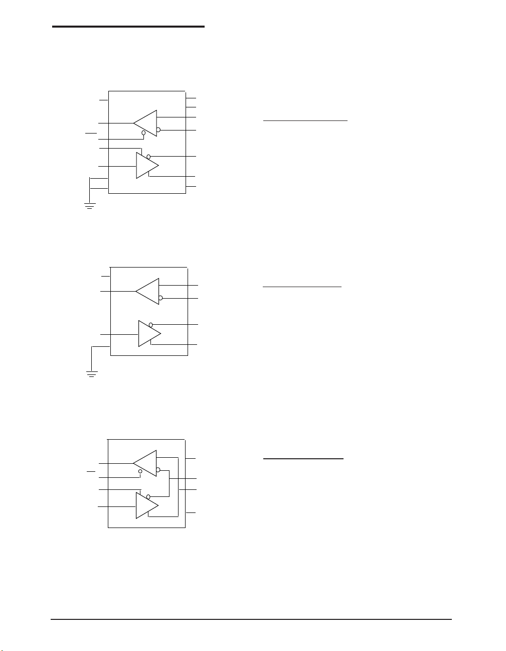
Devices are available in three industry standard architectures and footprints. In each footprint
there are three speed grades available.
14 Pin Full Duplex:
SP3070E, 250kbps slew limited
SP3073E, 500kbps slew limited
SP3076E, 16Mbps
8 Pin Full Duplex:
SP3071E, 250kbps slew limited
SP3074E, 500kbps slew limited
SP3077E, 16Mbps
8 Pin Half Duplex:
SP3072E, 250kbps slew limited
SP3075E, 500kbps slew limited
SP3078E, 16Mbps
Exar Corporation 48720 Kato Road, Fremont CA, 94538 • 510-668-7017 • www.exar.com SP3070E-SP3078E_102_120210
2
Page 3
These are stress ratings only and functional operation of the device at these
PARAMETER SYM. MIN. TYP. MAX. UNITS
®
CONDITIONS
Differential Driver Output V
OD
2 V
CC
V
RL = 100 (RS-422), Figure 1
1.5 V
CC
RL = 54 (RS-485), Figure 1
V
CC
®
No Load
Change in Magnitude of
Differential Output Voltage
V
OD
0.2 V
®
RL = 54 or 100, Figure 1
Driver Common Mode Output
Voltage
V
OC
VCC/2 3 V
®
RL = 54 or 100, Figure 1
Change in Magnitude of
Common Mode Output
Voltage
V
OC
±0.2 V RL = 54 or 100, Figure 1
Input High Voltage V
IH
2 V
®
DE, DI, RE
Input Low Voltage V
IL
0.8 V DE, DI, RE
Input Hysteresis V
HYS
100 mV
®
DE, DI, RE
Input Current I
IN
-1 1 µA
®
DE, DI, RE
Input Impedance First
Transition (Hotswap)
1 10 k
®
DE, RE
First transition will draw more
current (Hotswap)
Output Leakage (Y and Z)
Full Duplex (A and B)
I
O
+125
µA
®
DE = GND
VCC = GND or 3.6V
VIN= +12 V
-100
®
VIN= -7V
Driver Short-Circuit Current I
OSD
0 ±250
mA -7V V
OUT
12V, (Figure 4A)
-250 0
ratings or any other above those indicated in the operation sections of the
specications below is not implied. Exposure to absolute maximum rating
conditions for extended periods of time may affect reliability.
VCC.................................................................................................+6.0V
Input Voltage at control input pins (RE, DE).........................-0.3V to 6V
Driver Input Voltage (RE, DE)...............................................-0.3V to 6V
Driver Output Voltage (A, B, Y, & Z)....................................-8V to +13V
Receiver Input Voltage (A, B)..............................................-8V to +13V
Continuous Power Dissipation at TA = 70oC
8-pin SO (derate 5.88mW/oC above +70oC)................................471mW
ABSOLUTE MAXIMUM RATINGS
14-pin SO (derate 8.33mW/oC above +70oC).............. .............667mW
Operating Temperature Ranges
SP307XE_MN..............................................................-40ºC to +125ºC
SP307XE_EN ................................................................-40ºC to +85ºC
Junction Temperature.................................................................+150ºC
Storage Temperature Range.......................................-65ºC to +150º C
Lead Temperature (soldering, 10s) ..........................................+300º C
Unless otherwise noted V
ambient temperature TA = +25ºC. The ♦ denotes the specications which apply over the full operating range un-
= +3.3 ±0.3V, ambient temperature T
CC
less otherwise noted.
Exar Corporation 48720 Kato Road, Fremont CA, 94538 • 510-668-7017 • www.exar.com SP3070E-SP3078E_102_120210
ELECTRICAL CHARACTERISTICS
< TA < T
MIN
3
. Typical values are at VCC = 3.3,
MAX
Page 4
ELECTRICAL CHARACTERISTICS
PARAMETERS SYM MIN TYP MAX UNITS
®
CONDITIONS
Input Current (A and B)
Half Duplex
I
A,B
125
µA
®
DE = GND
VCC= GND or 3.6
VIN= +12V
-100 VIN= -7V
Thermal-Shutdown Threshold T
TS
165 ºC
®
Thermal Shutdown Hysteresis T
TSH
15 ºC
®
RECEIVER
Receiver Differential Threshold
(Sensitivity)
V
TH
-200 -125 -50 mV -7V VCM12 V
Receiver Input Hysteresis V
TH
15 mV
®
Va + Vb = 0V
RO Output High Voltage V
OH
Vcc -
0.6
V
®
IO = -1mA
RO Output Low Voltage V
OL
0.4 V
®
IO = 1mA
Tri-State Output Current at
Receiver
I
OZR
+/-1 µA
®
0 VO V
CC
Receiver Input Resistance R
IN
96 k
®
-7V VCM12 V
Receiver Output Short-Circuit
Current
I
OZR
±60 mA 0V VRO V
CC
SUPPLY CURRENT
Supply Current I
CC
0.8 1.5
mA
®
No Load, RE = 0, DE = V
CC
0.8 1.5 No Load, RE = VCC, DE = V
CC
0.8 1.5 No Load, RE = 0, DE = 0
Supply Current in Shutdown
mode
I
SHDN
0.05 3 µA RE = VCC, DE = GND
ESD PROTECTION
ESD Protection for Y, Z, A, and B
±15
kV
®
Human Body Model
±15 Air Gap (IEC 1000-4-2)
±8 Contact (IEC 1000-4-2)
Unless otherwise noted V
ambient temperature TA = +25ºC. The ♦ denotes the specications which apply over the full operating range un-
less otherwise noted.
= +3.3 ±0.3V, ambient temperature T
CC
< TA < T
MIN
. Typical values are at VCC = 3.3,
MAX
Exar Corporation 48720 Kato Road, Fremont CA, 94538 • 510-668-7017 • www.exar.com SP3070E-SP3078E_102_120210
4
Page 5
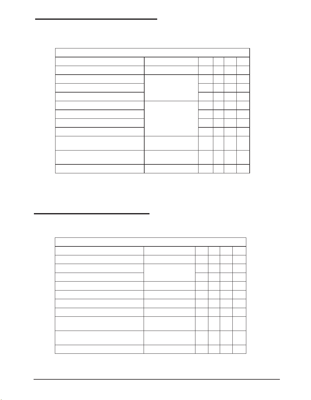
Unless otherwise noted V
= +3.3 ±0.3V, ambient temperature T
CC
ambient temperature TA = +25ºC.
SP3070E, SP3071E & SP3072E Driver Switching Characteristics
DRIVER CHARACTERISTICS: Conditions Min. Typ. Max. Unit
Data Signaling Rate Duty Cycle 40 to 60% 250 Kbps
Driver Propagation Delay (tPHL, tPLH)
Driver Output Rise/Fall Time (tR, tF) 350 1600 ns
Driver Differential Skew (tPLH – tPHL) 200 ns
Driver Enable to Output High (tZH)
Driver Enable to Output Low (tZL) 2500 ns
Driver Disable from Output High (tHZ) 100 ns
Driver Disable from Output Low (tLZ) 100 ns
Driver Enable from Shutdown to Output
High (tZH(SHDN))
Driver Enable from Shutdown to Output
Low (tZL(SHDN))
Time to Shutdown (tSHDN) 50 200 600 ns
DRIVER SWITCHING CHARACTERISTICS
< TA < T
MIN
RL = 54Ω, CL = 50pF,
Figure 2 & 3
RL = 500Ω, CL = 50pF,
Figure 4 & 5
Figure 4 5500 ns
Figure 5 5500 ns
. Typical values are at VCC = 3.3,
MAX
250 1500 ns
2500 ns
Unless otherwise noted V
= +3.3 ±0.3V, ambient temperature T
CC
ambient temperature TA = +25ºC.
SP3070E, SP3071E & SP3072E Receiver Switching Characteristics
RECEIVER CHARACTERISTICS: Conditions Min. Typ. Max. Unit
Data Signaling Rate Duty Cycle 40 to 60% 250 Kbps
Receiver Propagation Delay (tPLH, tPHL)
Propagation Delay Skew (tPLH, tPHL) 30 ns
Receiver Enable to Output High (tZH) Figure 8 50 ns
Receiver Enable to Output Low (tZL) Figure 8 50 ns
Receiver Disable from Output High (tHZ) Figure 8 100 ns
Receiver Disable from Output Low (tLZ) Figure 8 200 ns
Receiver Enable from Shutdown to Output
High
Receiver Enable from Shutdown to Output
Low
Time to Shutdown (tSHDN) 50 200 600 ns
Exar Corporation 48720 Kato Road, Fremont CA, 94538 • 510-668-7017 • www.exar.com SP3070E-SP3078E_102_120210
RECEIVER SWITCHING CHARACTERISTICS
< TA < T
MIN
Cl=15pF, Figure 6 & 7
Figure 8 4000 ns
Figure 8 4000 ns
. Typical values are at VCC = 3.3,
MAX
200 ns
5
Page 6
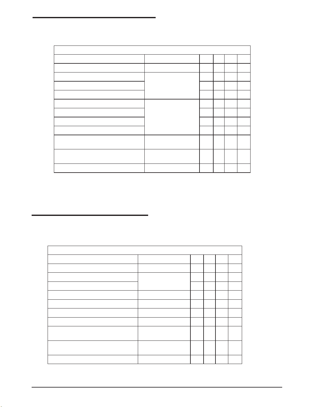
Unless otherwise noted V
= +3.3 ±0.3V, ambient temperature T
CC
ambient temperature TA = +25ºC.
SP3073E, SP3074E & SP3075E Driver Switching Characteristics
DRIVER CHARACTERISTICS: Conditions Min. Typ. Max. Unit
Data Signaling Rate Duty Cycle 40 to 60% 500 Kbps
Driver Propagation Delay (tPHL, tPLH)
Driver Output Rise/Fall Time (tR, tF) 200 800 ns
Driver Differential Skew (tPLH – tPHL) 100 ns
Driver Enable to Output High (tZH)
Driver Enable to Output Low (tZL) 2500 ns
Driver Disable from Output High (tHZ) 100 ns
Driver Disable from Output Low (tLZ) 100 ns
Driver Enable from Shutdown to Output
High (tZH(SHDN))
Driver Enable from Shutdown to Output
Low (tZL(SHDN))
Time to Shutdown (tSHDN) 50 200 600 ns
DRIVER SWITCHING CHARACTERISTICS
< TA < T
MIN
RL = 54Ω, CL = 50pF,
Figure 2 & 3
RL = 500Ω, CL = 50pF,
Figure 4 & 5
Figure 4 4500 ns
Figure 5 4500 ns
. Typical values are at VCC = 3.3,
MAX
180 800 ns
2500 ns
Unless otherwise noted V
ambient temperature TA = +25ºC.
SP3073E, SP3074E & SP3075E Receiver Switching Characteristics
RECEIVER CHARACTERISTICS: Conditions Min. Typ. Max. Unit
Data Signaling Rate Duty Cycle 40 to 60% 500 Kbps
Receiver Propagation Delay (tPLH, tPHL)
Propagation Delay Skew (tPLH, tPHL) 30 ns
Receiver Enable to Output High (tZH) Figure 8 50 ns
Receiver Enable to Output Low (tZL) Figure 8 50 ns
Receiver Disable from Output High (tHZ) Figure 8 50 ns
Receiver Disable from Output Low (tLZ) Figure 8 50 ns
Receiver Enable from Shutdown to Output
High
Receiver Enable from Shutdown to Output
Low
Time to Shutdown (tSHDN) 50 200 600 ns
Exar Corporation 48720 Kato Road, Fremont CA, 94538 • 510-668-7017 • www.exar.com SP3070E-SP3078E_102_120210
= +3.3 ±0.3V, ambient temperature T
CC
Cl=15pF, Figure 6 & 7
Figure 8 4000 ns
Figure 8 4000 ns
< TA < T
MIN
6
RECEIVER SWITCHING CHARACTERISTICS
. Typical values are at VCC = 3.3,
MAX
200 ns
Page 7
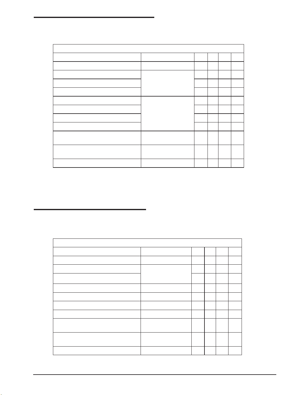
Unless otherwise noted Vcc=+3.3±0.3V, ambient temperature Tmin < Ta < Tmax. Typical values are at Vcc = 3.3,
DRIVER SWITCHING CHARACTERISTICS
ambient temperature Ta = +25ºC
SP3076E, SP3077E & SP3078E Driver Switching Characteristics
DRIVER CHARACTERISTICS: Conditions Min. Typ. Max. Unit
Data Signaling Rate Duty Cycle 40 to 60% 16 Mbps
Driver Propagation Delay (tPHL, tPLH)
Driver Output Rise/Fall Time (tR, tF) 15 ns
Driver Differential Skew (tPLH – tPHL) 8 ns
Driver Enable to Output High (tZH)
Driver Enable to Output Low (tZL) 150 ns
Driver Disable from Output High (tHZ) 100 ns
Driver Disable from Output Low (tLZ) 100 ns
Driver Enable from Shutdown to Output
High (tZH(SHDN))
Driver Enable from Shutdown to Output
Low (tZL(SHDN))
Time to Shutdown (tSHDN) 50 200 600 ns
RL = 54Ω, CL = 50pF,
Figure 2 & 4
RL = 500Ω, CL = 50pF,
Figure 4 & 5
Figure 4 1800 ns
Figure 5 1800 ns
50 ns
150 ns
RECEIVER SWITCHING CHARACTERISTICS
Unless otherwise noted Vcc=+3.3±0.3V, ambient temperature Tmin < Ta < Tmax. Typical values are at Vcc = 3.3,
ambient temperature Ta = +25ºC
SP3076E, SP3077E & SP3078E Receiver Switching Characteristics
RECEIVER CHARACTERISTICS: Conditions Min. Typ. Max. Unit
Data Signaling Rate Duty Cycle 40 to 60% 16 Mbps
Receiver Propagation Delay (tPLH, tPHL) Cl=15pF, Figure 6 & 7,
Propagation Delay Skew (tPLH, tPHL) 8 ns
Receiver Enable to Output High (tZH) Figure 8 60 ns
Receiver Enable to Output Low (tZL) Figure 8 60 ns
Receiver Disable from Output High (tHZ) Figure 8 50 ns
Receiver Disable from Output Low (tLZ) Figure 8 50 ns
Receiver Enable from Shutdown to Output
High
Receiver Enable from Shutdown to Output
Low
Time to Shutdown (tSHDN) 50 200 600 ns
Exar Corporation 48720 Kato Road, Fremont CA, 94538 • 510-668-7017 • www.exar.com SP3070E-SP3078E_102_120210
-40 to +85 ºC
Figure 8 3000 ns
Figure 8 3000 ns
40 75 ns
7
Page 8
Y
Z
D
DI
RL
54
CL
50pF
3.3V
VOD
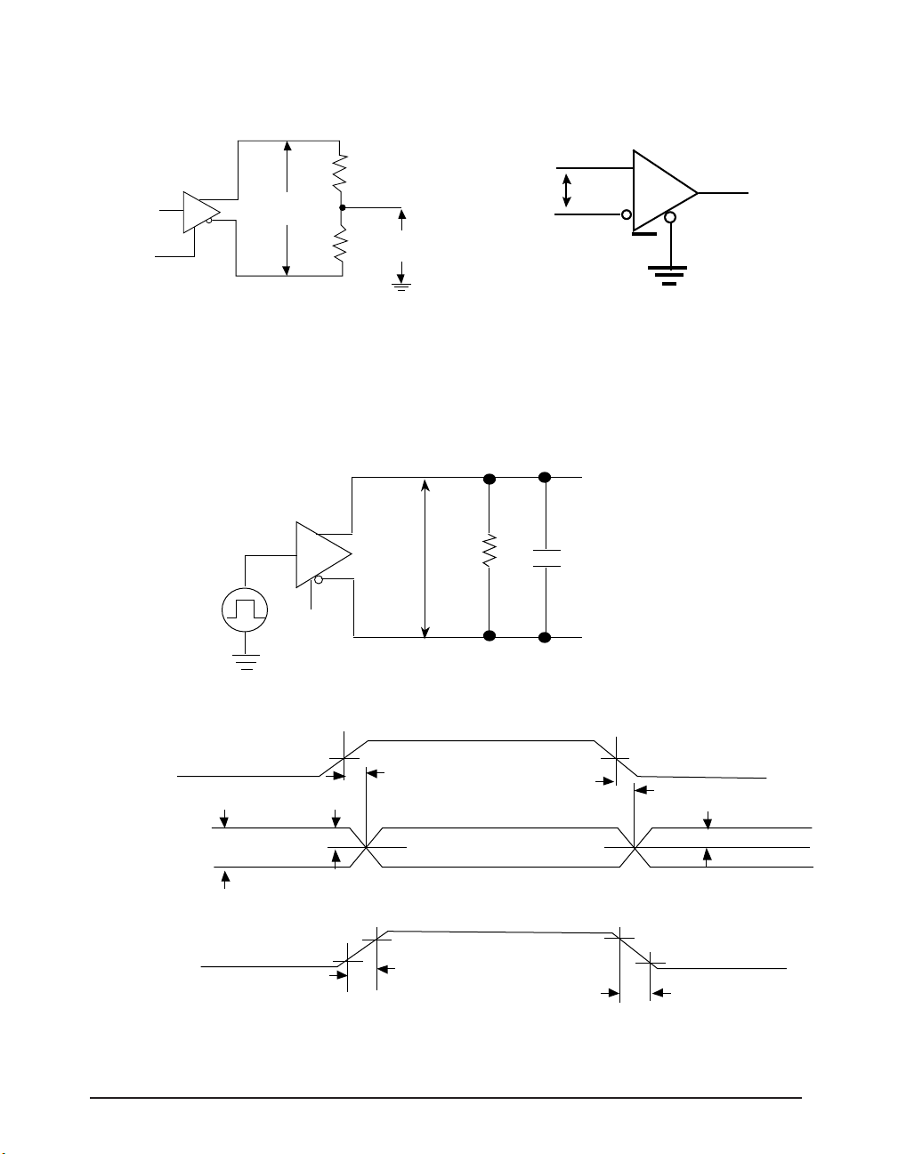
FIGURE 1. DRIVER DC TEST CIRCUIT
t
PHL
t
PLH
Z
Y
10%
90%
10%
90%
V
SKEW
= t
PLH - tPHL
V
DIFF
= V(Y) - V(Z)
V
O
V
CC
VCC/2
0
DI
V
DIFF
-V
O
1/2 V
O
t
R
t
F
V
O
1/2 V
O
OUT
R
A
B
VID
RE
R/2
R/2
V
OC
D
V
CC
V
OD
D
I
0 or 3V
FIGURE 2. RECEIVER DC TEST CIRCUIT
FIGURE 3. DRIVER PROPAGATION DELAY TIME TEST CIRCUIT AND TIMING DIAGRAM
Exar Corporation 48720 Kato Road, Fremont CA, 94538 • 510-668-7017 • www.exar.com SP3070E-SP3078E_102_120210
8
Page 9
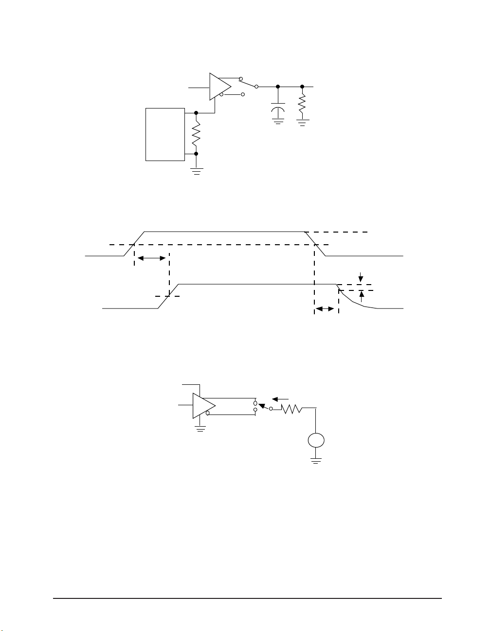
FIGURE 4. DRIVER ENABLE & DISABLE TIMES TEST CIRCUIT & TIMING DIAGRAM
GENERATOR
50W
S1
RL = 500W
OUT
CL = 50pF
D0 or VCC
Z
Y
DI
DE
t
LZ
0.25V
OUT
V
CC
VOM = (VOL+ VCC)/2
t
ZL, tZL(SHDN
V
CC
/2
0
0
A/Y
DDI = 0 or 3V
B/Z
DE = 0 or 3V
IOSD
100
-7V to +12V V
FIGURE 4A. DRIVER CONTENTION TEST
Exar Corporation 48720 Kato Road, Fremont CA, 94538 • 510-668-7017 • www.exar.com SP3070E-SP3078E_102_120210
9
Page 10
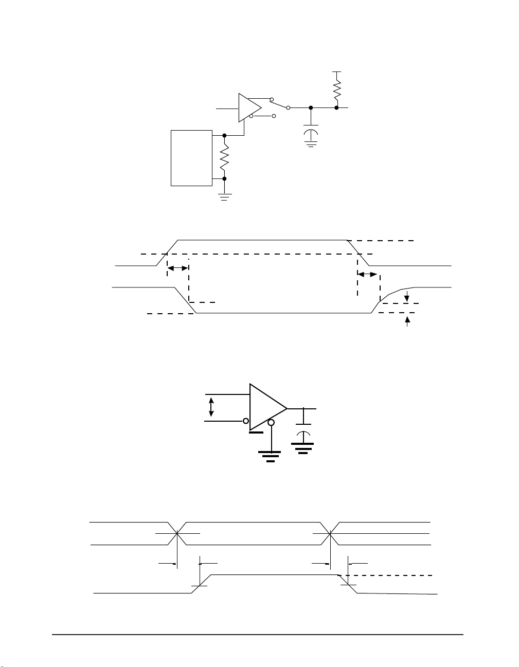
FIGURE 5. DRIVER ENABLE & DISABLE TIMES TEST CIRCUIT & TIMING DIAGRAM
DE
V
OL
t
LZ
0.25V
VCC OUT
V
CC
VOM = (VOL+ VCC)/2
t
ZL, tZL(SHDN
V
CC
/2
0
OUT
R
A
B
VID
RE
CL
15pF
t
PHL
t
PLH
V
OL
1.5V
OUT
V
OH
A
B
+1V
-1V
GENERATOR
50W
S1
RL = 500W
OUT
CL = 50pF
D0 or VCC
Z
Y
DI
VCC
FIGURE 6. RECEIVER PROPAGATION DELAY TEST CIRCUIT & TIMING DIAGRAM
10
Exar Corporation 48720 Kato Road, Fremont CA, 94538 • 510-668-7017 • www.exar.com SP3070E-SP3078E_102_120210
Page 11
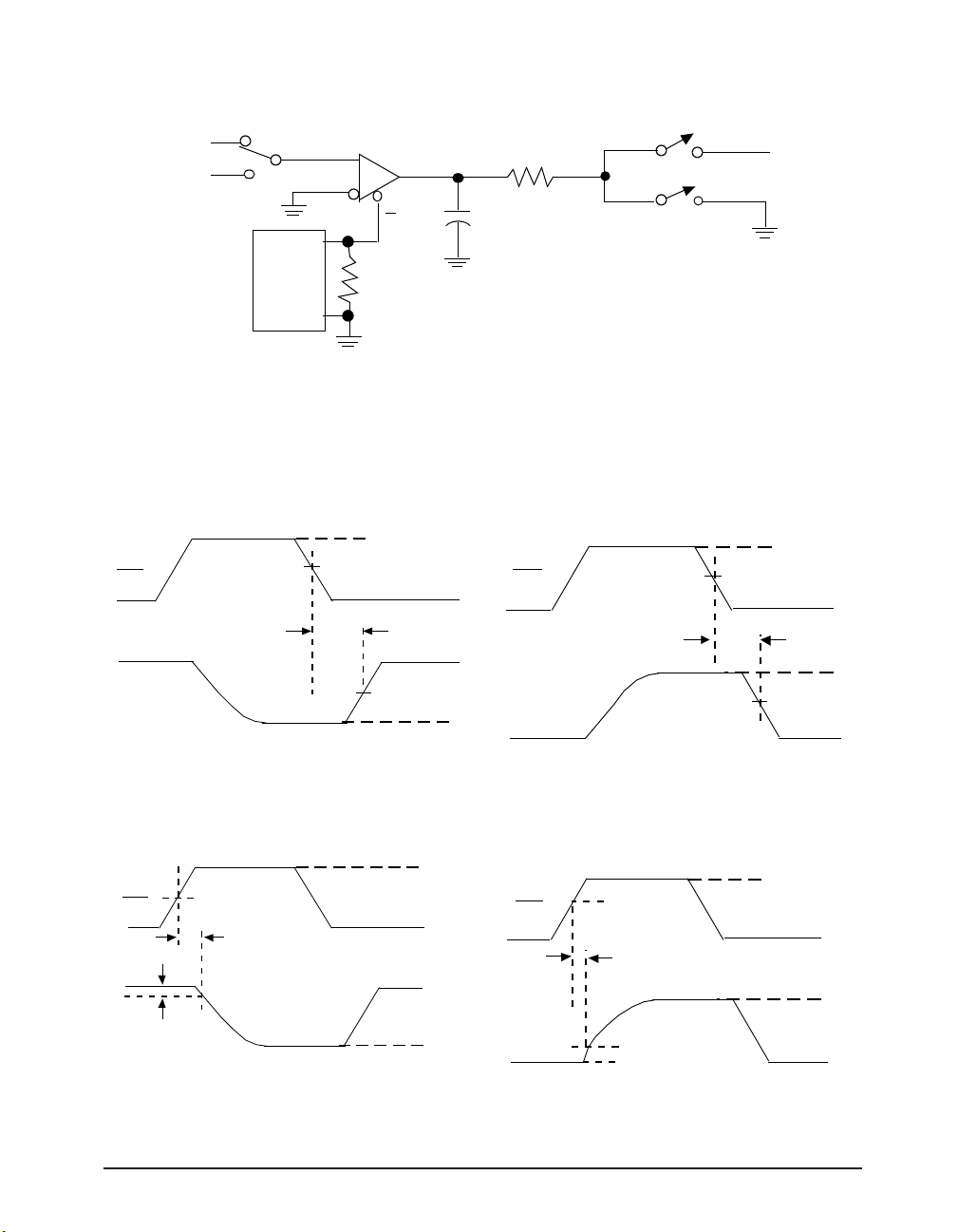
FIGURE 7. RECEIVER ENABLE & DISABLE TIMES TEST CIRCUIT
1.5V
-1.5V
S3
A
GENERATOR
50W
CL = 15pF
R
1kW
S1
S2
VCC
B
RE
3V
0V
1.5V
V
CC
RE
OUT
S1 is closed, S2 is open, S3 = -1.5V
t
ZL, tZL(SHDN)
V
OL
= VCC/2
V
OL
3V
0V
1.5V
V
CC
RE
OUT
S1 is closed, S2 is open, S3 = -1.5V
t
LZ
V
OL
0.25V
3V
1.5V
0V
RE
OUT
S1 is open S2 is closed S3 = 1.5V
V
OH
t
HZ
0.25V
3V
1.5V
0V
RE
OUT
S1 is open S2 is closed S3 = 1.5V
V
OH
t
ZH, tZH(SHDN)
VOH/2
FIGURE 8. RECEIVER ENABLE & DISABLE TIMING DIAGRAM
Exar Corporation 48720 Kato Road, Fremont CA, 94538 • 510-668-7017 • www.exar.com SP3070E-SP3078E_102_120210
11
Page 12
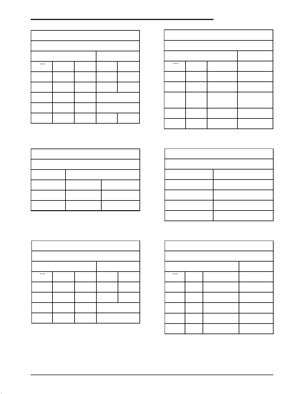
FUNCTION TABLES
SP3070E, SP3073E, SP3076E (Full Duplex)
TRANSMITTING
Inputs Outputs
RE DE DI Z Y
X 1 1 0 1
X 1 0 1 0
0 0 X High-Z
1 0 X Shutdown
SP3070E, SP3073E, SP3076E (Full Duplex)
RECEIVING
Inputs Output
RE DE A, B RO
0 X -50mV 1
0 X - 200 mV 0
X X Open,
Shorted
1
1 1 X High-Z
1 0 X Shutdown
SP3072E, SP3075E, SP3078E (Half Duplex)
TRANSMITTING
Inputs Outputs
RE DE DI B/Z A/Y
X 1 1 0 1
X 1 0 1 0
0 0 X High-Z
1 0 X Shutdown
SP3072E, SP3075E, SP3078E (Half Duplex)
RECEIVING
Inputs Output
RE DE A, B RO
0 X - 50 mV 1
0 X - 200mV 0
X X Open/shorted 1
1 1 X High-Z
1 0 X Shutdown
SP3071E, SP3074E, SP3077E (Full Duplex)
TRANSMITTING
Inputs Outputs
DI Z Y
1 0 1
0 1 0
SP3071E, SP3074E, SP3077E (Full Duplex)
RECEIVING
Inputs Output
A, B RO
-50mV 1
- 200mV 0
Open/shorted 1
Exar Corporation 48720 Kato Road, Fremont CA, 94538 • 510-668-7017 • www.exar.com SP3070E-SP3078E_102_120210
12
Page 13
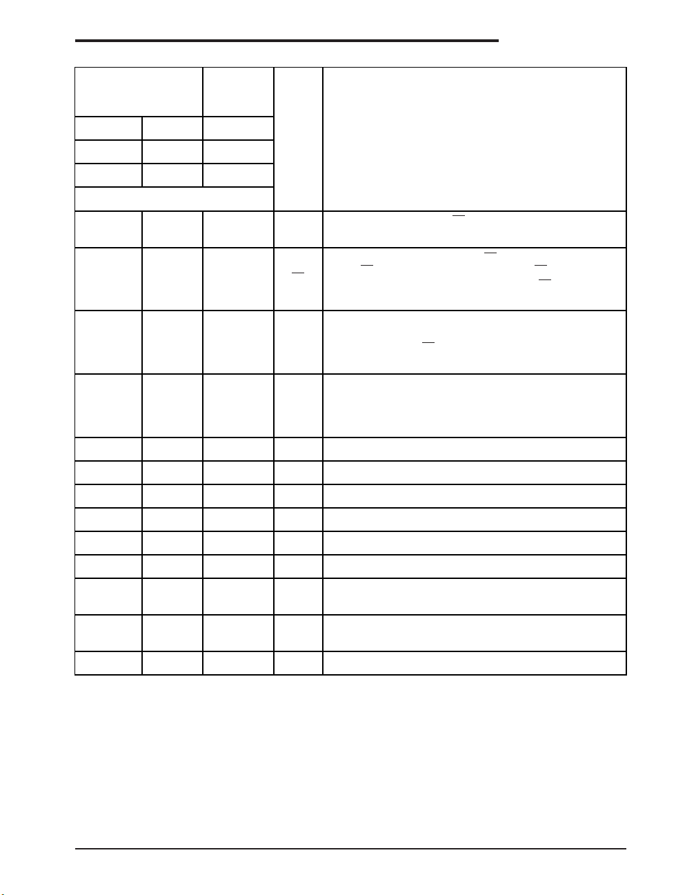
PIN DESCRIPTION
FULL DUPLEX
DEVICES
HALF
DUPLEX
DEVICES
PIN
NAME
PIN FUNCTION
SP3070E SP3071E SP3072E
SP3073E SP3074E SP3075E
SP3076E SP3077E SP3078E
PIN NUMBER
2 2 1 RO
Receiver Output. When RE is low and if (A – B)
-50mV, RO is High. If (A – B) - 200mV, RO is low.
3 - 2 RE
Receiver Output Enable. When RE is low, RO is enabled.
When RE is high, RO is high impedance. RE should be
high and DE low to enter shutdown mode. RE is a hotswap input.
4 - 3 DE
Driver Output Enable. When DE is high, outputs are
enabled. When DE is low, outputs are high impedance. DE
should be low and RE high to enter shutdown mode. DE is
a hot-swap input.
5 3 4 DI
Driver Input. With DE high, a low level on DI forces
noninverting output low and inverting output high. Similarly,
a high level on DI forces noninverting output high and
inverting output low.
6, 7 4 5 GND Ground
9 5 - Y Noninverting Driver Output
10 6 - Z Inverting Driver Output
11 7 - B Inverting Receiver Input
- - 7 B Inverting Receiver Input and Inverting Driver Output
12 8 - A Noninverting Receiver Input
- - 6 A
Noninverting Receiver Input and Noninverting Driver
Output
14 1 8 V
CC
Positive Supply VCC. Bypass VCC to GND with a 0.1uF
capacitor.
1, 8, 13 - - NC No Connect
Exar Corporation 48720 Kato Road, Fremont CA, 94538 • 510-668-7017 • www.exar.com SP3070E-SP3078E_102_120210
13
Page 14

DETAILED DESCRIPTION
The SP307XE family of high speed transceivers for RS-485/RS-422 communication
contain one driver and one receiver. These
devices feature fail-safe circuitry, which
guarantees a logic-high receiver output when
the receiver inputs are open or shorted, or
when they are connected to a terminated
transmission line with all drivers disabled. The
SP3070E, SP3072E, SP3073E, SP3075E,
SP3076E and SP3078E also feature a
hotswap capability allowing live insertion
without error data transfer. The SP3070E,
SP3071E and SP3072E feature reduced
slew-rate drivers that minimize EMI and
reduce reections caused by improperly
terminated cables, allowing error-free data
transmission up to 250kbps. The SP3073E,
SP3074E and SP3075E also offer slew -rate
limits allowing transmit speeds up to 500kbps.
The SP3076E, SP3077E, SP3078E driver
slew rates are not limited, making transmit
speeds up to 16Mbps possible.
The SP3072E, SP3075E and SP3078E are
half-duplex transceivers, while the SP3070E,
SP3071E, SP3073E, SP3074E, SP3076E,
and SP3077E are full duplex transceivers.
All devices operate from a single 3.3V supply.
Drivers are output short-circuit current limited.
Thermal-shutdown circuitry protects drivers
against excessive power dissipation. When
activated, the thermal-shutdown circuitry
places the driver outputs into a high-impedance state.
RECEIVER INPUT FILTERING
SP3070E-SP3075E receivers incorporate
input ltering in addition to input hysteresis.
This ltering enhances noise immunity with
differential signals that have very slow rise
and fall times. Receiver propagation delay
increases by 25% due to this ltering.
FAIL SAFE
The SP3070E family guarantees a logic-high
receiver output when the receiver inputs are
shorted, open, or when they are connected
to a terminated transmission line with all
drivers disabled. If A - B is less than or equal
DETAILED DESCRIPTION
to -200mV, RO is logic low. In the case of a
terminated bus with all transmitters disabled
the receiver's differential input voltage is
pulled to ZeroV by the termination. With the
receiver thresholds of the SP3070E family,
this results in a logic high with a 50mV minimum noise margin. In compliance with the
EIA/TIA-485 standard, the SP3070E family
has a 50mV - 200mV threshold.
HOT-SWAP CAPABILITY
When circuit boards are inserted into a hot
backplane, differential disturbances to the
data bus can lead to data errors. Upon initial
circuit board insertion, the data communication processor undergoes its own power-up
sequence. During this period, the processor's
logic-output drivers are high impedance and
are unable to drive the DE and RE inputs
of these devices to a dened logic level.
Leakage currents up to 10µA from the highimpedance state of the processor's logic
drivers could cause standard CMOS enable
inputs of a transceiver to drift to an incorrect logic level. Additionally, parasitic circuit
board capacitance could cause coupling of
VCC or GND to the enable inputs. Without
the hot-swap capability, these factors could
improperly enable the transceiver's driver
or receiver.
When VCC rises, an internal pulldown circuit
holds DE low and RE high for approximately
10 microseconds. After the initial power-up
sequence, the pulldown circuit becomes
transparent, resetting the hot-swap tolerable input.
15KV ESD PROTECTION
As with all Exar devices, ESD-protection
structures are incorporated on all pins to
protect against electrostatic discharges
encountered during handling and assembly.
The driver output and receiver inputs of
the SP3070E family of devices have extra
protection against static electricity. Exar's
engineering team have developed state
of the art structures to protect these pins
against ESD of 15kV without damage. The
Exar Corporation 48720 Kato Road, Fremont CA, 94538 • 510-668-7017 • www.exar.com SP3070E-SP3078E_102_120210
14
Page 15

DETAILED DESCRIPTION
ESD structures withstand high ESD in all
states: normal operation, shutdown, and
powered down. After an ESD event, the
SP3070E - SP3078E keep working without
latchup or damage.
ESD protection can be tested in various ways.
The transmitter outputs and receiver inputs of
the SP3070E - SP3078E are characterized
for protection to the following limits:
■ ±15kV using the Human Body Model
■ ±8kV using the Contact Discharge method
specied in IEC 61000-4-2
■ ±15kV Airgap
ESD TEST CONDITIONS
ESD performance depends on a variety
of conditions. Contact Exar for a reliability
report that documents test setup, methodology and results.
IEC 61000-4-2
The IEC 61000-4-2 standard covers ESD
testing and performance of nished equipment. However, it does not specically refer
to integrated circuits. The SP3070E family
of devices helps you design equipment to
meet IEC 61000-4-2, without the need for
additional ESD-protection components.
The major difference between tests done
using the Human Body Model and IEC
61000-4-2 is higher peak current in IEC
61000-4-2, because series resistance is
lower in the IEC 1000-4-2 model. Hence,
the ESD withstand voltage measured to
EC 61000-4-2 is generally lower than that
measured using the human body model.
The air-gap test involves approaching the
device with a charged probe. The contactdischarge method connects the probe to the
device before the probe is energized.
256 TRANSCEIVERS ON THE BUS
The standard RS-485 receiver input imped-
ance is 12kΩ (1 unit load), and the standard
driver can drive up to 32 unit loads. The
SP3070E family of transceivers has a 1/8-
unit load receiver input impedance (96kΩ),
allowing up to 256 transceivers to be connected in parallel on one communication
line. Any combination of these devices as
well as other RS-485 transceivers with a
total of 32 unit loads or fewer can be connected to the line.
REDUCED EMI AND REFLECTIONS
The SP3070E, SP3071E and SP3072E
feature reduced slew-rate drivers that mini-
mize EMI and reduce reections caused by
improperly terminated cables, allowing error-free data transmission up to 250kbps.
The SP3073E, SP3074E and SP3075E offer
higher driver output slew-rate limits, allowing
transmit speeds up to 500kbps.
LOW POWER SHUTDOWN MODE
Low-power shutdown mode is initiated by
bringing both RE high and DE low. In shutdown, the devices typically draw only 50nA
of supply current.
RE and DE can be driven simultaneously;
the parts are guaranteed not to enter shutdown if RE is high and DE is low for less
than 50ns. If the inputs are in this state for
at least 600ns, the parts are guaranteed to
enter shutdown.
Enable times tZH and tZL assume the part was
not in a low-power shutdown state. Enable
times t
were shut down. It takes drivers and receivers
ZH(SHDN)
and t
assume the parts
ZL(SHDN)
longer to become enabled from low-power
shutdown mode t
driver/receiver-disable mode (tZH, tZL)
ZH(SHDN)
and t
ZL(SHDN)
than from
MACHINE MODEL
The machine model for ESD tests all pins
using a 200pF storage capacitor and zero
discharge resistance. The objective is to
emulate the stress caused when I/O pins
are contacted by handling equipment during
test and assembly.
Exar Corporation 48720 Kato Road, Fremont CA, 94538 • 510-668-7017 • www.exar.com SP3070E-SP3078E_102_120210
DRIVER OUTPUT PROTECTION
Two mechanisms prevent excessive output
current and power dissipation caused by
faults or by bus contention. First, current
limit on the ouput stage, provides immediate protection against short circuits over the
whole common-mode voltage range.
15
Page 16
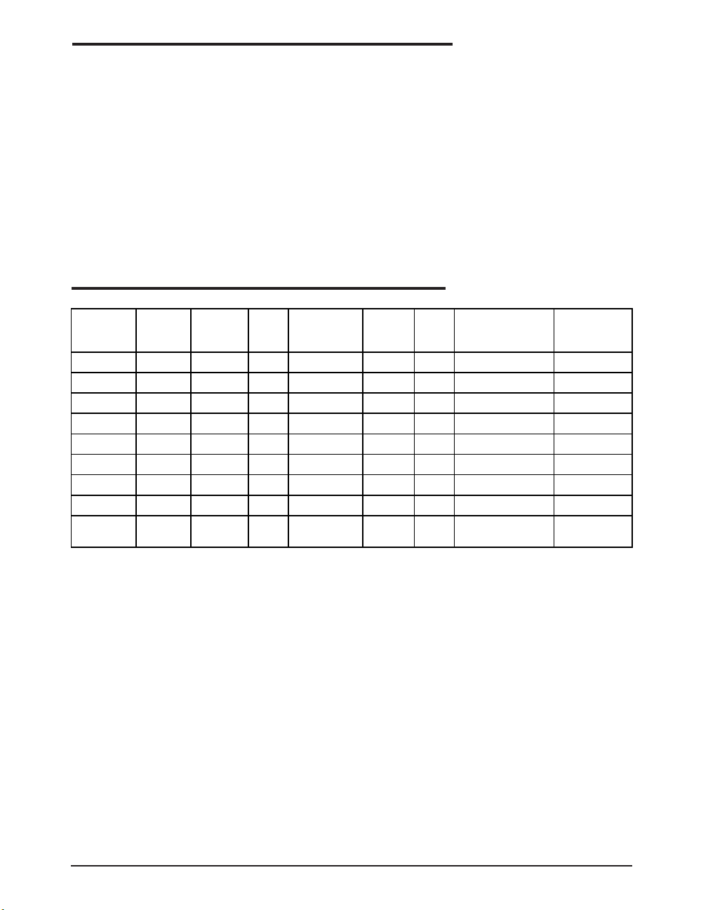
Second, a thermal-shutdown circuit, forces
PART
NUMBER
Half/Full
Duplex
Datarate
Mbps
Shutdown
Receiver
Driver Enable
Trans.
On Bus
Pin
Count
Industry Standard
Pinout
Pin
Compatible
Upgrade from:
SP3070E Full 0.25 Yes Yes 256 14 MAX3070E, 75180
SP3071E Full 0.25 No No 256 8 MAX 3071E, 75179 SP3493
SP3072E Half 0.25 Yes Yes 256 8 MAX 3072E, 75176 SP3483
SP3073E Full 0.5 Yes Yes 256 14 MAX 3073E, 75180
SP3074E Full 0.5 No No 256 8 MAX 3074E, 75179
SP3075E Half 0.5 Yes Yes 256 8 MAX 3075E, 75176 SP3494
SP3076E Full 16 Yes Yes 256 14 MAX 3076E, 75180 SP3491
SP3077E Full 16 No No 256 8 MAX3077E, 75179 SP3490
SP3078E Half 16 Yes Yes
256 8
MAX 3078E, 75176 SP3485,
SP3481
the driver outputs into a high-impedance
state if the die temperature becomes excessive.
LINE LENGTH
The RS-485/RS422 standard covers line
lengths up to 4000ft.
TYPICAL APPLICATIONS
The SP3072E, SP3075E and SP3078E
transceivers are designed for bidirectional
data communications on multipoint bus
transmission lines.
DETAILED DESCRIPTION
To minimize reections, terminate the line at
both ends in its characteristic impedance,
and keep stub lengths off the main line as
short as possible. The slew-rate-limited
SP3070E - SP3075E are more tolerant of
imperfect termination.
PARTS SELECTOR GUIDE
Exar Corporation 48720 Kato Road, Fremont CA, 94538 • 510-668-7017 • www.exar.com SP3070E-SP3078E_102_120210
16
Page 17
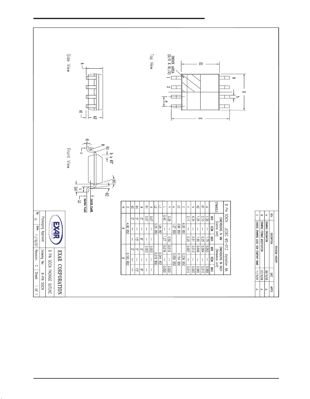
PACKAGE: 8 PIN NSOIC
Exar Corporation 48720 Kato Road, Fremont CA, 94538 • 510-668-7017 • www.exar.com SP3070E-SP3078E_102_120210
17
Page 18
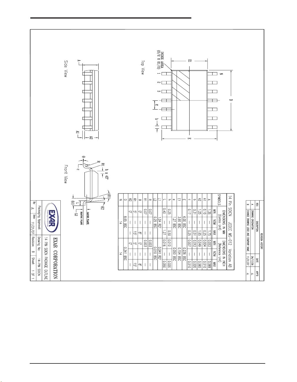
PACKAGE: 14 PIN NSOIC
Exar Corporation 48720 Kato Road, Fremont CA, 94538 • 510-668-7017 • www.exar.com SP3070E-SP3078E_102_120210
18
Page 19

ORDERING INFORMATION
Model Temperature Range Package
SP3070EEN-L ..................................................-40˚C to +85˚C...................................................... 14-pin NSOIC
SP3070EEN-L/TR ............................................-40˚C to +85˚C...................................................... 14-pin NSOIC
SP3070EMN-L ................................................-40˚C to +125˚C..................................................... 14-pin NSOIC
SP3070EMN-L/TR...........................................-40˚C to +125˚C..................................................... 14-pin NSOIC
SP3071EEN-L ..................................................-40˚C to +85˚C........................................................ 8-pin NSOIC
SP3071EEN-L/TR ............................................-40˚C to +85˚C........................................................ 8-pin NSOIC
SP3071EMN-L ................................................-40˚C to +125˚C....................................................... 8-pin NSOIC
SP3071EMN-L/TR...........................................-40˚C to +125˚C....................................................... 8-pin NSOIC
SP3072EEN-L ..................................................-40˚C to +85˚C........................................................ 8-pin NSOIC
SP3072EEN-L/TR ............................................-40˚C to +85˚C........................................................ 8-pin NSOIC
SP3072EMN-L ................................................-40˚C to +125˚C....................................................... 8-pin NSOIC
SP3072EMN-L/TR...........................................-40˚C to +125˚C....................................................... 8-pin NSOIC
SP3073EEN-L ..................................................-40˚C to +85˚C...................................................... 14-pin NSOIC
SP3073EEN-L/TR ............................................-40˚C to +85˚C...................................................... 14-pin NSOIC
SP3073EMN-L ................................................-40˚C to +125˚C..................................................... 14-pin NSOIC
SP3073EMN-L/TR...........................................-40˚C to +125˚C..................................................... 14-pin NSOIC
SP3074EEN-L ..................................................-40˚C to +85˚C........................................................ 8-pin NSOIC
SP3074EEN-L/TR ............................................-40˚C to +85˚C........................................................ 8-pin NSOIC
SP3074EMN-L ................................................-40˚C to +125˚C....................................................... 8-pin NSOIC
SP3074EMN-L/TR...........................................-40˚C to +125˚C....................................................... 8-pin NSOIC
SP3075EEN-L ..................................................-40˚C to +85˚C........................................................ 8-pin NSOIC
SP3075EEN-L/TR ............................................-40˚C to +85˚C........................................................ 8-pin NSOIC
SP3075EMN-L ................................................-40˚C to +125˚C....................................................... 8-pin NSOIC
SP3075EMN-L/TR...........................................-40˚C to +125˚C....................................................... 8-pin NSOIC
SP3076EEN-L ..................................................-40˚C to +85˚C...................................................... 14-pin NSOIC
SP3076EEN-L/TR ............................................-40˚C to +85˚C...................................................... 14-pin NSOIC
SP3076EMN-L ................................................-40˚C to +125˚C..................................................... 14-pin NSOIC
SP3076EMN-L/TR...........................................-40˚C to +125˚C..................................................... 14-pin NSOIC
SP3077EEN-L ..................................................-40˚C to +85˚C........................................................ 8-pin NSOIC
SP3077EEN-L/TR ............................................-40˚C to +85˚C........................................................ 8-pin NSOIC
SP3077EMN-L ................................................-40˚C to +125˚C....................................................... 8-pin NSOIC
SP3077EMN-L/TR...........................................-40˚C to +125˚C....................................................... 8-pin NSOIC
SP3078EEN-L ..................................................-40˚C to +85˚C........................................................ 8-pin NSOIC
SP3078EEN-L/TR ............................................-40˚C to +85˚C........................................................ 8-pin NSOIC
SP3078EMN-L ................................................-40˚C to +125˚C....................................................... 8-pin NSOIC
SP3078EMN-L/TR...........................................-40˚C to +125˚C....................................................... 8-pin NSOIC
For availability of PDIP or other packaging contact factory.
Available in lead free packaging. To order add “-L” sufx to part number.
Example: SP3074EEN/TR = standard; SP3074EEN-L/TR = lead free
/TR = Tape and Reel
Pack quantity is 2,500 for NSOIC.
Exar Corporation 48720 Kato Road, Fremont CA, 94538 • 510-668-7017 • www.exar.com SP3070E-SP3078E_102_120210
19
Page 20
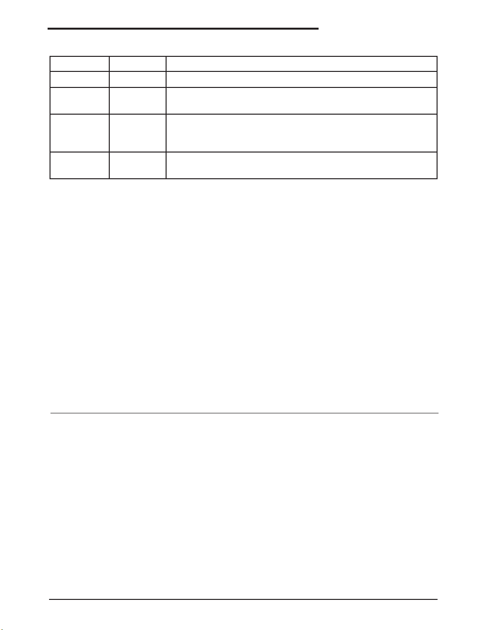
OTHER INFORMATION
DATE REVISION DESCRIPTION
Legacy Sipex Datasheet
06/10/09 1.0.0 Convert to Exar format, update ordering information, correct
subscript on pages 5-7 and change revision to 1.0.0
09/30/10 1.0.1 Correct type error on page 7 on driver switching character-
istics table. Change SP3076E,3077E and 3078E Receiver
enable time from shutdown from 1800ns to 3000ns.
12/02/10 1.0.2 Add reference to Application Note ANI#21 and change ESD
protection levels to IEC 61000-4-2.
Notice
EXAR Corporation reserves the right to make changes to any products contained in this publication in order to improve design, performance or reliability. EXAR Corporation assumes no representation that the circuits are free of patent infringement. Charts and schedules contained herein are
only for illustration purposes and may vary depending upon a user's specic application. While the information in this publication has been carefully
checked;
no responsibility, however, is assumed for inaccuracies.
EXAR Corporation does not recommend the use of any of its products in life support applications where the failure or malfunction of the product can
reasonably be expected to cause failure of the life support system or to signicantly affect its safety or effectiveness. Products are not authorized for
use in such applications unless EXAR Corporation receives, in writting, assurances to its satisfaction that: (a) the risk of injury or damage has been
minimized ; (b) the user assumes all such risks; (c) potential liability of EXAR Corporation is adequately protected under the circumstances.
Copyright 2010 EXAR Corporation
Datasheet December 2010
For technical support please email Exar's Serial Technical Support group at: [email protected]
Reproduction, in part or whole, without the prior written consent of EXAR Corporation is prohibited.
Exar Corporation 48720 Kato Road, Fremont CA, 94538 • 510-668-7017 • www.exar.com SP3070E-SP3078E_102_120210
20
 Loading...