Maxim Integrated Producs ICL7665ACJA, ICL7665ACPA, ICL7665ACSA, ICL7665ACTV, ICL7665AEPA Datasheet
...
_______________General Description
The ICL7665 warns microprocessors (µPs) of overvoltage and undervoltage conditions. It draws a typical
operating current of only 3µA. The trip points and hysteresis of the two voltage detectors are individually programmed via external resistors to any voltage greater
than 1.3V. The ICL7665 will operate from any supply
voltage in the 1.6V to 16V range, while monitoring voltages from 1.3V to several hundred volts. The Maxim
ICL7665A is an improved version with a 2%-accurate
V
SET
1
threshold and guaranteed performance over
temperature.
The 3µA quiescent current of the ICL7665 makes it
ideal for voltage monitoring in battery-powered systems. In both battery- and line-powered systems, the
unique combination of a reference, two comparators,
and hysteresis outputs reduces the size and component count of many circuits.
________________________Applications
µP Voltage Monitoring
Low-Battery Detection
Power-Fail and Brownout Detection
Battery Backup Switching
Power-Supply Fault Monitoring
Over/Undervoltage Protection
High/Low Temperature, Pressure, Voltage Alarms
____________________________Features
♦ µP Over/Undervoltage Warning
♦ Improved Second Source
♦ Dual Comparator with Precision Internal Reference
♦ 3µA Operating Current
♦ 2% Threshold Accuracy (ICL7665A)
♦ 1.6V to 16V Supply Voltage Range
♦ On-Board Hysteresis Outputs
♦ Externally Programmable Trip Points
♦ Monolithic, Low-Power CMOS Design
______________Ordering Information
Ordering Information continued on last page.
ICL7665
Microprocessor Voltage Monitor with
Dual Over/Undervoltage Detection
________________________________________________________________
Maxim Integrated Products
1
1
2
3
4
8
7
6
5
OUT2
SET2
HYST2
GND
SET1
HYST1
OUT1
ICL7665
DIP/SO
TOP VIEW
2
8
4
6
1
7
3
5
ICL7665
V+ (CASE)
HYST2
SET2
OUT2
OUT1
HYST1
SET1
TO-99
GND
V+
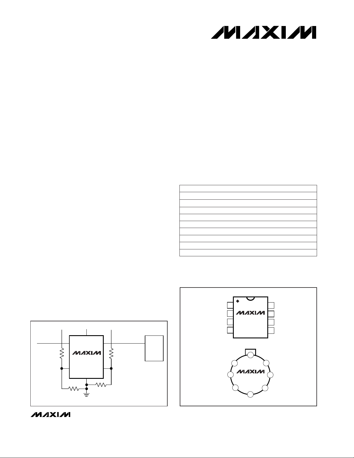
_________________Pin Configurations
ICL7665
OUT1
OUT2
SET2
SET1
V+ V
IN2
V
IN1
V+
8
4
1
7
6
3
GND
OVERVOLTAGE
DETECTION
UNDERVOLTAGE
DETECTION
SIMPLE THRESHOLD DETECTOR
NMI
__________Typical Operating Circuit
19-0001; Rev 2; 8/97
PART TEMP. RANGE PIN-PACKAGE
ICL7665CPA 0°C to +70°C 8 Plastic DIP
ICL7665ACPA 0°C to +70°C 8 Plastic DIP
ICL7665BCPA 0°C to +70°C 8 Plastic DIP
ICL7665CSA 0°C to +70°C 8 SO
ICL7665ACSA 0°C to +70°C 8 SO
ICL7665BCSA 0°C to +70°C 8 SO
ICL7665CJA 0°C to +70°C 8 CERDIP
ICL7665ACJA 0°C to +70°C 8 CERDIP
ICL7665BCJA 0°C to +70°C 8 CERDIP
For free samples & the latest literature: http://www.maxim-ic.com, or phone 1-800-998-8800.
For small orders, phone 408-737-7600 ext. 3468.

ICL7665
Microprocessor Voltage Monitor with
Dual Over/Undervoltage Detection
2 _______________________________________________________________________________________
ABSOLUTE MAXIMUM RATINGS
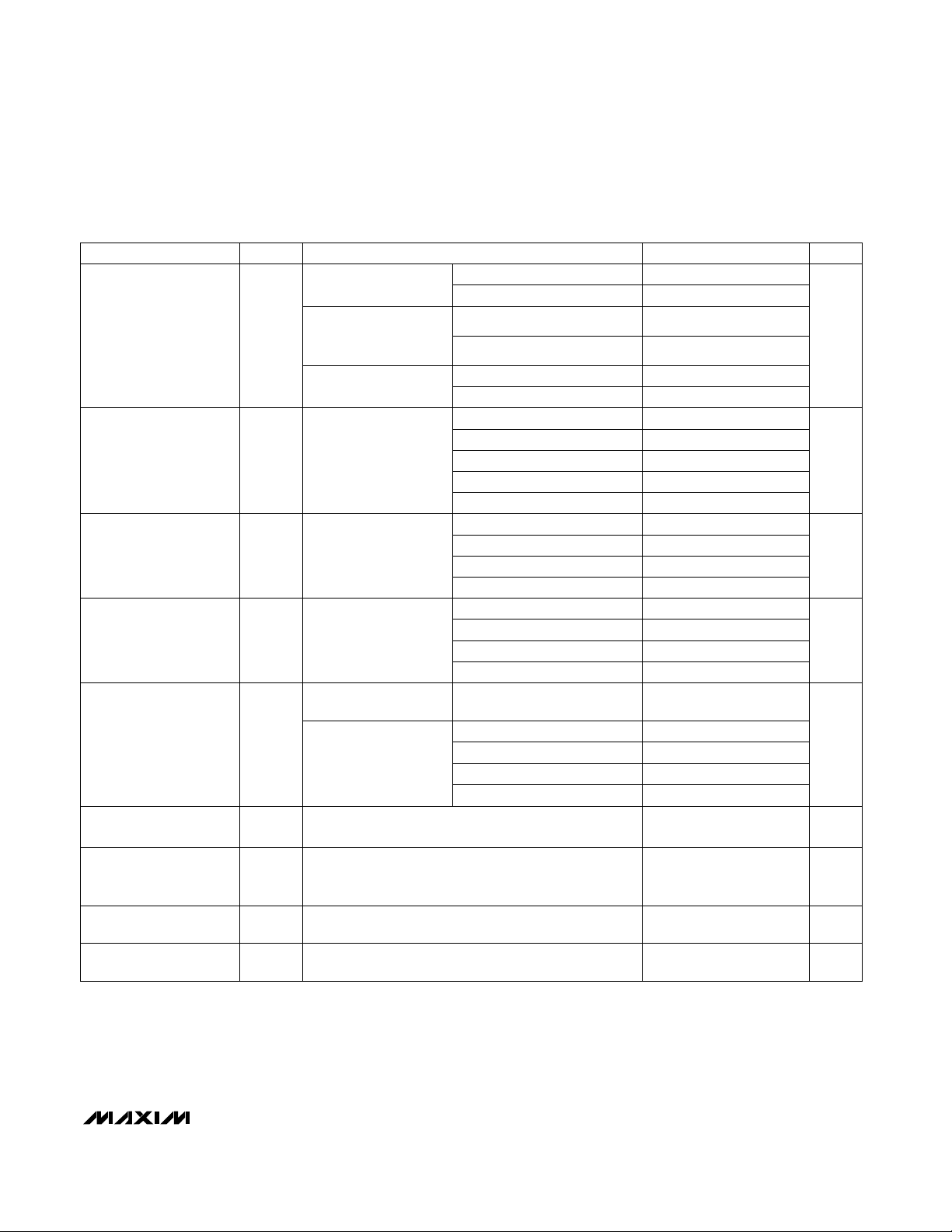
ELECTRICAL CHARACTERISTICS
(V+ = 5V, TA= +25°C, unless otherwise noted.)
Stresses beyond those listed under “Absolute Maximum Ratings” may cause permanent damage to the device. These are stress ratings only, and functional
operation of the device at these or any other conditions beyond those indicated in the operational sections of the specifications is not implied. Exposure to
absolute maximum rating conditions for extended periods may affect device reliability.
Note 1: Due to the SCR structure inherent in the CMOS process used to fabricate these devices, connecting any terminal to volt-
ages greater than (V+ + 0.3V) or less than (GND - 0.3V) may cause destructive latchup. For this reason, we recommend
that inputs from external sources that are not operating from the same power supply not be applied to the device before its
supply is established, and that in multiple supply systems, the supply to the ICL7665 be turned on first. If this is not possible, currents into inputs and/or outputs must be limited to ±0.5mA and voltages must not exceed those defined above.
Supply Voltage (Note 1).........................................-0.3V to +18V
Output Voltages OUT1 and OUT2
(with respect to GND) (Note 1)..........................-0.3V to +18V
Output Voltages HYST1 and HYST2
(with respect to V+) (Note 1) .............................+0.3V to -18V
Input Voltages SET1 and SET2
(Note 1)........................................(GND - 0.3V) to (V+ + 0.3V)
Maximum Sink Output Current
OUT1 and OUT2.............................................................25mA
Maximum Source Output Current
HYST1 and HYST2........................................................-25mA
Continuous Power Dissipation (T
A
= +70°C)
Plastic DIP (derate 9.09mW/°C above +70°C)............727mW
SO (derate 5.88mW/°C above +70°C)........................471mW
CERDIP (derate 8.00mW/°C above +70°C)................640mW
TO-99 (derate 6.67mW/°C above +70°C)...................533mW
Operating Temperature Ranges
ICL7665C_ _.......................................................0°C to +70°C
ICL7665I_ _.....................................................-20°C to +85°C
ICL7665E_ _....................................................-40°C to +85°C
Storage Temperature Range.............................-65°C to +160°C
Lead Temperature (soldering, 10sec).............................+300°C
PARAMETER
SYMBOL CONDITIONS
MIN TYP MAX
UNITS
Operating Supply Voltage V+
ICL7665
TA= +25°C 1.6 16
V
TA = T
MIN
to T
MIN
1.8 16
ICL7665A TA = T
MIN
to T
MIN
2.0 16
ICL7665B
TA= +25°C 1.6 10
Input Trip Voltage V
SET
ICL7665, ICL7665B, TA= +25°C
V
SET1
1.150 1.300 1.450
V
V
SET2
1.200 1.300 1.400
ICL7665A, TA= +25°C
V
SET1
1.275 1.300 1.325
V
SET2
1.225 1.300 1.375
ICL7665A, TA= T
MIN
to T
MAX
V
SET1
1.250 1.300 1.350
V
SET2
1.215 1.300 1.385
V
SET
Tempco 100 ppm/°C
R
OUT1
, R
OUT2
, R
HYST1
, R
HYST2
= 1MΩ 0.004 %/V
Supply Current I+
GND ≤ V
SET1,
V
SET2
≤
V+,
all outputs open
circuit
V+ = 2V 2.5 10
µA
V+ = 9V 2.6 10
V+ = 15V 2.9 15
ICL7665B,
TA= +25°C
V+ = 2V 2.5 10
V+ = 9V 2.6 10
TA = T
MIN
to T
MIN
1.8 10
ICL7665,
TA= +25°C;
ICL7665A,
TA= T
MIN
to T
MAX
Supply Voltage Sensitivity
of V
SET1
, V
SET2

ICL7665
Microprocessor Voltage Monitor with
Dual Over/Undervoltage Detection
_______________________________________________________________________________________ 3
ELECTRICAL CHARACTERISTICS (continued)
(V+ = 5V, TA= +25°C, unless otherwise noted.)
PARAMETER
CONDITIONS
MIN TYP MAX
UNITS
Output Leakage Current I
OLK
,
I
HLK
All grades, V
SET
= 0V or
V
SET
≥ 2V, TA= +25°C
OUT1, OUT2 10 200
nA
HYST1, HSYT2 -10 -100
OUT1, OUT2 2000
HYST1, HSYT2 -500
ICL7665B, V+ = 9V,
TA= T
MIN
to T
MAX
OUT1, OUT2 2000
HYST1, HSYT2 -500
V
OUT1
Saturation
Voltage
V
SET1
= 2V,
I
OUT1
= 2mA
ICL7665, ICL7665B: V+ = 2V 0.20 0.50
ICL7665A: V+ = 2V 0.20
All grades: V+ = 5V 0.10 0.30
ICL7665, ICL7665A: V+ = 15V 0.06 0.20
ICL7665B: V+ = 9V 0.06 0.25
All grades: V+ = 2V -0.15 -0.30
All grades: V+ = 5V -0.05 -0.15
ICL7665, ICL665A: V+ = 15V -0.02 -0.10
ICL7665B: V+ = 9V
-0.02 -0.15
V
OUT2
Saturation
Voltage
V
SET2
= 0V,
I
OUT2
= 2mA
All grades: V+ = 2V 0.20 0.50
V
All grades: V+ = 5V 0.15 0.30
ICL7665, ICL665A: V+ = 15V 0.11 0.25
ICL7665B: V+ = 9V 0.11 0.30
V
HYST2
Saturation
Voltage
All grades: V+ = 2V -0.25 -0.80
V
All grades: V+ = 5V -0.43 -1.00
ICL7665: V+ = 15V -0.35 -0.80
ICL7665A: V+ = 15V -0.35 -1.00
ICL7665B: V+ = 9V -0.35 -1.00
I
SET
GND ≤ V
SET
≤ V+
±0.01 ±10 nA
∆V
SET
0.1 mV
V
SET1
–
V
SET2
±5 ±50 mV
±0.1 mV
SYMBOL
V
V
HYST1
Saturation
Voltage
V
V
SET1
= 2V,
I
HYST1
= -0.5mA
ICL7665, ICL7665A,
V+ = 15V,
TA= T
MIN
to T
MAX
V
SET2
= 2V,
I
HYST2
= -0.2mA
V
SET2
= 2V,
I
HYST2
= -0.5mA
V
SET
Input Leakage
Current
R
OUT
, R
HYST
= 1MΩ
R
OUT
, R
HYST
= 1MΩ
R
OUT
= 4.7kΩ, R
HYST
= 20kΩ,
V
OUT
LO = 1% V+, V
OUT
HI = 99% V+
V
SET
Input Change for
Complete Output
Change
Difference in Trip
Voltage
Output/Hysteresis
Difference

ICL7665
Microprocessor Voltage Monitor with
Dual Over/Undervoltage Detection
4 _______________________________________________________________________________________
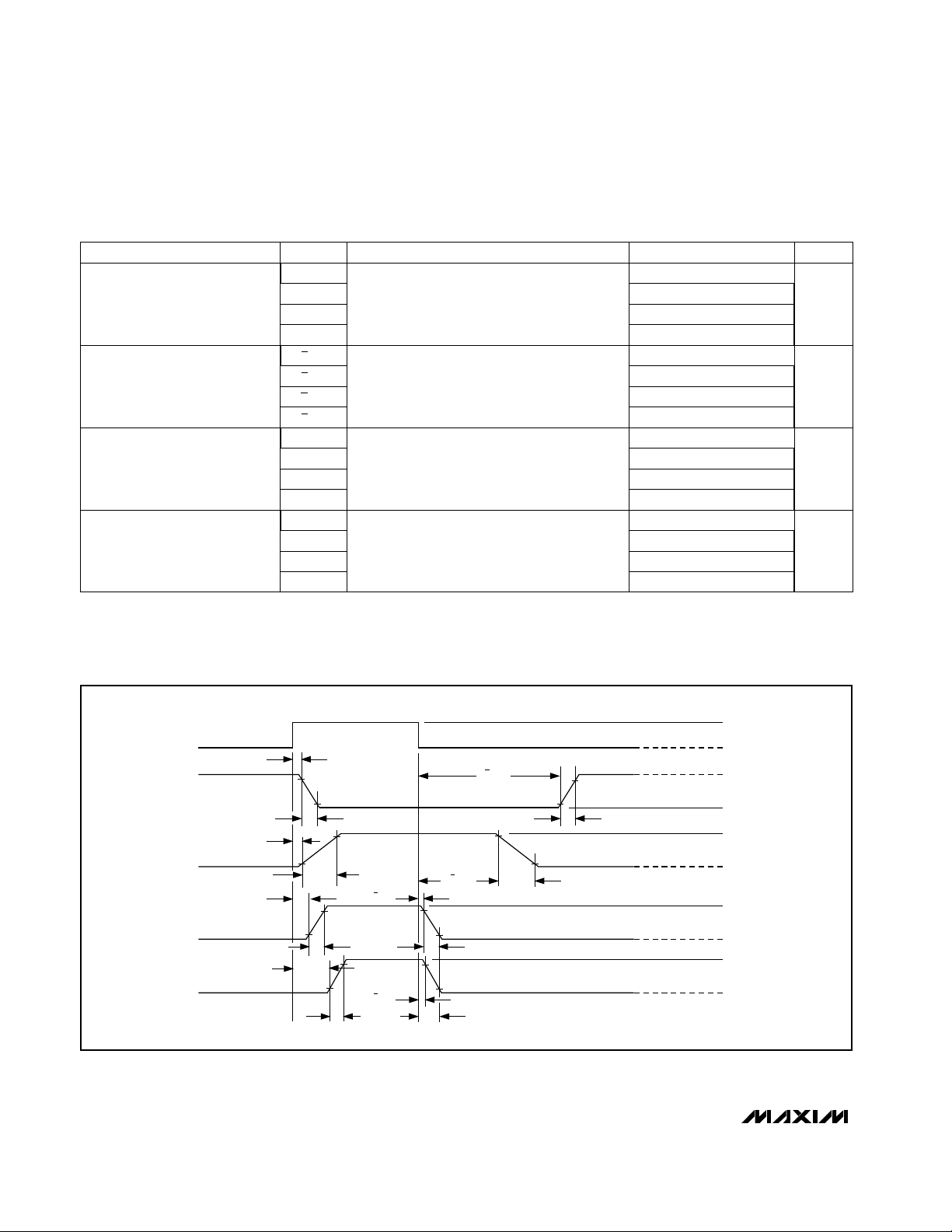
AC OPERATING CHARACTERISTICS
(V+ = 5V, TA= +25°C, unless otherwise noted.)
V
SET
switched between 1.0V and 1.6V,
R
OUT
= 4.7kΩ, CL= 12pF,
R
HYST
= 20kΩ
µs
1.8t
H2f
Output Fall Times
4.0t
H1f
0.7t
O2f
0.6t
O1f
V
SET
switched between 1.0V and 1.6V,
R
OUT
= 4.7kΩ, CL= 12pF,
R
HYST
= 20kΩ
µs
0.7t
H2r
Output Rise Times
7.5t
H1r
0.8t
O2r
0.6t
O1r
V
SET
switched from 1.6V to 1.0V,
R
OUT
= 4.7kΩ, CL= 12pF,
R
HYST
= 20kΩ
µs
60t
SH2d
Output Delay Time,
Input Going Low
60t
SO2d
80t
SH1d
75t
SO1d
V
SET
switched from 1.0V to 1.6V,
R
OUT
= 4.7kΩ, CL= 12pF,
R
HYST
= 20kΩ
CONDITIONS
µs
55t
SH2d
Output Delay Time,
Input Going High
55t
SO2d
90t
SH1d
85t
SO1d
UNITSMIN TYP MAXSYMBOLPARAMETER
_______________________________________________________Switching Waveforms
INPUT
OUT1
HYST1
OUT2
HYST2
V
SET1,VSET2
t
SO1d
t
SH1d
t
SO2d
t
SH2d
t
SO1d
t
O1f
t
H1r
t
SO2d
t
O2r
t
SH2d
t
H2r
t
SH1d
t
H1f
t
O2f
t
H2f
t
O1r
1.6V
1.0V
V+ (5V)
GND
V+ (5V)
GND
V+ (5V)
GND
V+ (5V)
GND
 Loading...