Rev 1; 2/08
PART TEMP RANGE PIN-PACKAGE
DS8113-RNG+ -40°C to +85°C 28 SO
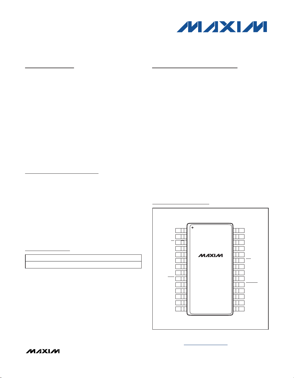
PGND
28
27
26
25
24
23
22
AUX2IN
AUX1IN
I/OIN
XTAL2
TOP VIEW
DS8113
XTAL1
OFF
GND
21 VDD
20 RSTIN
19 CMDVCC
18 1_8V
17 VCC
16 RST
15 CLK
5V/3V
CLKDIV2
CLKDIV1
CP1
VDDA
VUP
PRES
PRES
I/O
AUX2
AUX1
4
1
2
3
5
6
7
8
9
10
11
12
13
14CGND
CP2
SO
Smart Card Interface
General Description
The DS8113 smart card interface is a low-cost, analog
front-end for a smart card reader, designed for all ISO
7816, EMV™, and GSM11-11 applications. The DS8113
supports 5V, 3V, and 1.8V smart cards. The DS8113
provides options for low active- and stop-mode power
consumption, with as little as 10nA stop-mode current.
The DS8113 is designed to interface between a system
microcontroller and the smart card interface, providing
all power supply, ESD protection, and level shifting
required for IC card applications.
An EMV Level 1 certified library (written for the MAXQ2000
microcontroller) and hardware reference design is
available. Contact Maxim technical support at
micro.support@maxim-ic.com regarding requirements for
other microcontroller platforms. An evaluation kit,
DS8113-KIT, is available to aid in prototyping and
evaluation.
Applications
Consumer Set-Top Boxes
Access Control
Banking Applications
POS Terminals
Debit/Credit Payment Terminals
PIN Pads
Automated Teller Machines
Telecommunications
Pay/Premium Television
Features
♦ Analog Interface and Level Shifting for IC Card
Communication
♦ 8kV (min) ESD (IEC) Protection on Card Interface
♦ Ultra-Low Stop-Mode Current, Less Than 10nA
Typical
♦ Internal IC Card Supply-Voltage Generation:
5.0V ±5%, 80mA (max)
3.0V ±8%, 65mA (max)
1.8V ±10%, 30mA (max)
♦ Automatic Card Activation and Deactivation
Controlled by Dedicated Internal Sequencer
♦ I/O Lines from Host Directly Level Shifted for
Smart Card Communication
♦ Flexible Card Clock Generation, Supporting
External Crystal Frequency Divided by 1, 2, 4, or 8
♦ High-Current, Short-Circuit and High-Temperature
Protection
♦ Low Active-Mode Current
Pin Configuration
DS8113
Ordering Information
Note: Contact the factory for availability of other variants and
package options.
+Denotes a lead-free package.
Selector Guide appears at end of data sheet.
EMV is a trademark owned by EMVCo LLC.
Note: Some revisions of this device may incorporate deviations from published specifications known as errata. Multiple revisions of any device may be
simultaneously available through various sales channels. For information about device errata, go to:
For pricing, delivery, and ordering information, please contact Maxim Direct at 1-888-629-4642,
or visit Maxim’s website at www.maxim-ic.com.
________________________________________________________________ Maxim Integrated Products 1
www.maxim-ic.com/errata.
Smart Card Interface
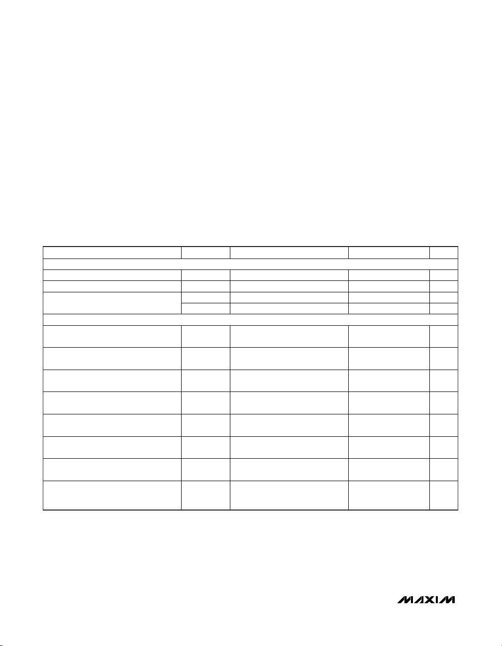
PARAMETER SYMBOL CONDITIONS MIN TYP MAX UNITS
POWER SUP PLY
Digital Supply Voltage V
DD
2.7 6.0 V
Card Voltage-Generator Supply Volt age V
DDA
V
DDA
> V
DD
5.0 6.0 V
V
TH2
Thresho ld volt age (falling) 2.35 2.45 2.55 V
Reset Voltage Thresholds
V
HYS2
Hysteresi s 50.0 100 150 mV
CURRENT CONSUMPTION
Acti ve VDDCurrent 5V Cards
(Including 80mA Draw from 5V Card)
I
DD_50V
ICC= 80mA, f
XTAL
= 20MHz,
f
CLK
= 10MHz, V
DDA
= 5.0V
80.75 85.00 mA
Acti ve VDDCurrent 5V Cards
(Current Con sumed by DS8113 Only)
I
DD_IC
ICC= 80mA, f
XTAL
= 20MHz,
f
CLK
= 10MHz, V
DDA
= 5.0V (Note 2)
0.75 5.00 mA
Acti ve VDDCurrent 3V Cards
(Including 65mA Draw from 3V Card)
I
DD_30V
ICC= 65mA, f
XTAL
= 20MHz,
f
CLK
= 10MHz, V
DDA
= 5.0V
65.75 70.00 mA
Acti ve VDDCurrent 3V Cards
(Current Con sumed by DS8113 Only)
I
DD_IC
ICC= 65mA, f
XTAL
= 20MHz,
f
CLK
= 10MHz, V
DDA
= 5.0V (Note 2)
0.75 5.00 mA
Acti ve VDDCurrent 1.8V Cards
(Including 30mA Draw from 1.8V Card)
I
DD_18V
ICC= 30mA, f
XTAL
= 20MHz,
f
CLK
= 10MHz, V
DDA
= 5.0V
30.75 35.00 mA
Acti ve VDDCurrent 1.8V Cards
(Current Con sumed by DS8113 Only)
I
DD_IC
ICC= 30mA, f
XTAL
= 20MHz,
f
CLK
= 10MHz, V
DDA
= 5.0V (Note 2)
0.75 5.00 mA
Inacti ve-Mode Current I
DD
Card inact ive, act ive-high PRES,
DS8113 not in stop mode
50.0 200 µA
Stop-Mode Current I
DD_STOP
DS8113 in ultra-low-power stop
mode (CMDVCC, 5V/3V, and 1 _8V
set to l og ic 1) (Note 3)
0.01 2.00 µA
ABSOLUTE MAXIMUM RATINGS
Voltage Range on VDD Relative to GND...............-0.5V to +6.5V
oltage Range on VDDA Relative to PGND ..........-0.5V to +6.5V
V
Voltage Range on CP1, CP2, and VUP
Relative to PGND...............................................-0.5V to +7.5V
oltage Range on All Other Pins
V
Relative to GND......................................-0.5V to (V
DS8113
Stresses beyond those listed under “Absolute Maximum Ratings” may cause permanent damage to the device. These are stress ratings only, and functional
operation of the device at these or any other conditions beyond those indicated in the operational sections of the specifications is not implied. Exposure to
absolute maximum rating conditions for extended periods may affect device reliability.
DD
+ 0.5V)
RECOMMENDED DC OPERATING CONDITIONS
(VDD= +3.3V, V
= +5.0V, TA= +25°C, unless otherwise noted.) (Note 1)
DDA
Maximum Junction Temperature .....................................+125°C
aximum Power Dissipation (T
M
Storage Temperature Range .............................-55°C to +150°C
-25°C to +85°C) .......700mW
=
A
Soldering Temperature.........Refer to the IPC/JEDEC J-STD-020
pecification.
S
2 _______________________________________________________________________________________
Smart Card Interface
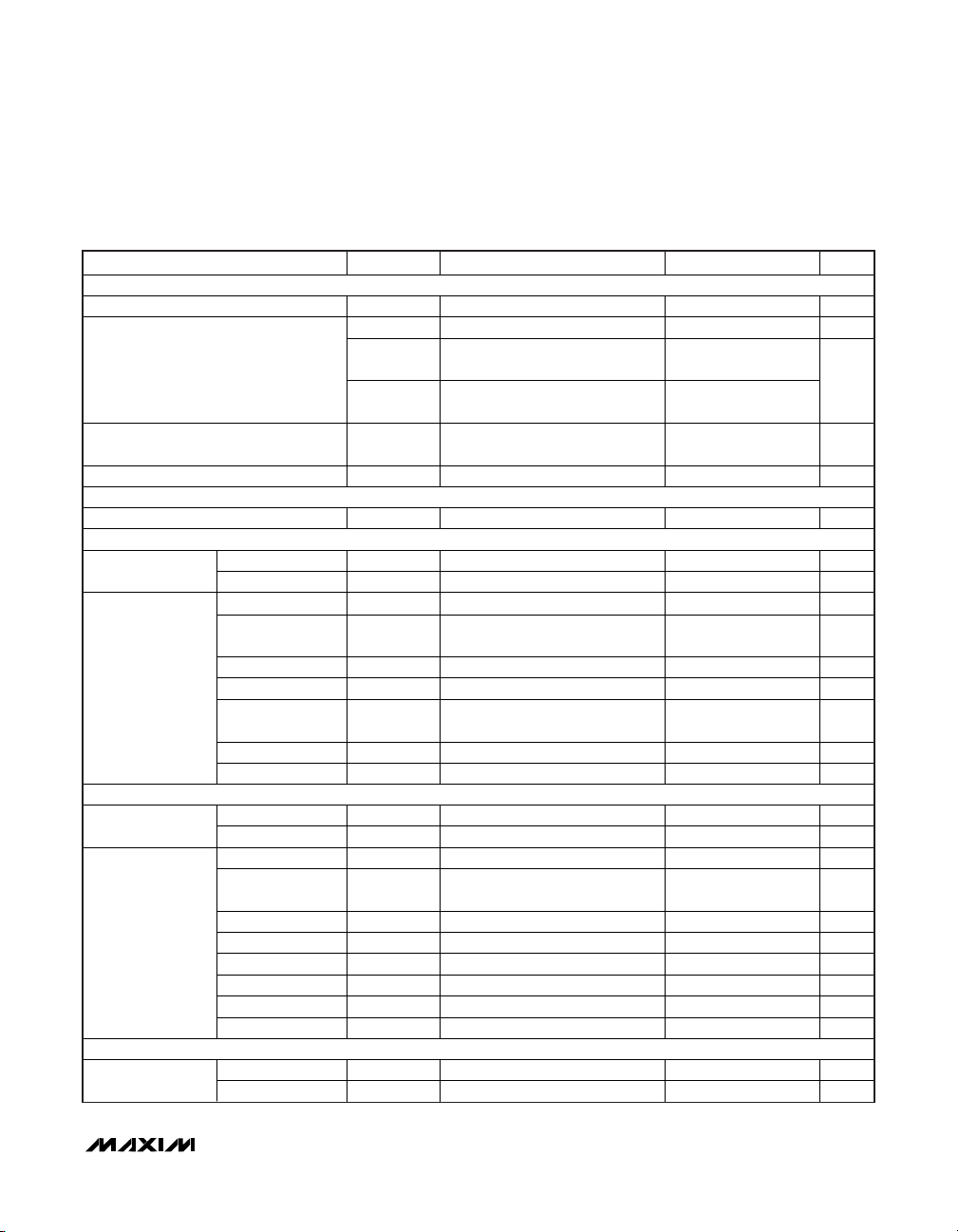
PARAMETER SYMBOL CONDITIONS MIN TYP MAX UNITS
CLOCK SOURCE
Crysta l Frequency f
XTAL
External crystal 0 20 MHz
f
XTAL1
0 20 MHz
V
IL_XTAL1
Low-level input on XTAL1 -0.3
0.3 x
V
D
D
XTAL1 Operating Condit ions
V
IH_XTAL1
High-level input on XTAL1
0.7 x
V
DD
VDD+
0.3
V
External Capacitance for Cryst al
C
XTAL1
,
C
XTAL2
15 pF
Internal Osc illator f
INT
2.2 2.7 3.2 MHz
SHUTDOWN TEMPERATURE
Shutdown Temperature T
SD
+150 °C
RST PIN
Output Low Volt age V
OL_RST1IOL_RST
= 1mA 0 0.3 V
Card-Inactive Mode
Output Current I
OL_RST1VO_LRST
= 0V 0 -1 mA
Output Low Volt age V
OL_RST2IOL_RST
= 200µA 0 0.3 V
Output H igh
Voltage
V
OH_RST2IOH_RST
= -200µA
V
CC
-
0.5
V
CC
V
Rise Tim e t
R_RST
CL= 30pF 0.1 µ s
Fall Time t
F_RST
CL= 30pF 0.1 µ s
Shutdown Current
Thresho ld
I
RST(SD)
-20 mA
Current Lim itation I
RST(LIMIT)
-20 +20 mA
Card-Active Mode
RSTIN to RST Delay t
D(RSTIN-RST)
2 µs
CLK PIN
Output Low Volt age V
OL_CLK1IOLCLK
= 1mA 0 0.3 V
Card-Inactive Mode
Output Current I
OL_CLK1VOLCLK
= 0V 0 -1 mA
Output Low Volt age V
OL_CLK2IOLCLK
= 200µA 0 0.3 V
Output H igh
Voltage
V
OH_CLK2IOHCLK
= -200µA
V
CC
-
0.5
V
CC
V
Rise Tim e t
R_CLK
CL= 30pF (Note 4) 8 ns
Fall Time t
F_CLK
CL= 30pF (Note 4) 8 ns
Current Lim itation I
CLK(LIMIT)
-70 +70 mA
Clock Freq uenc y f
CLK
Operational 0 10 MHz
Duty Fact or CL= 30pF 45 55 %
Card-Active Mode
Slew Rate SR C
L
= 30pF 0.2 V/ns
VCC PIN
Output Low Volt age V
CC1
ICC= 1mA 0 0.3 V
Card-Inactive Mode
Output Current I
CC1
VCC= 0V 0 -1 mA
RECOMMENDED DC OPERATING CONDITIONS (continued)
(VDD= +3.3V, V
= +5.0V, TA= +25°C, unless otherwise noted.) (Note 1)
DDA
_______________________________________________________________________________________ 3
DS8113
Smart Card Interface
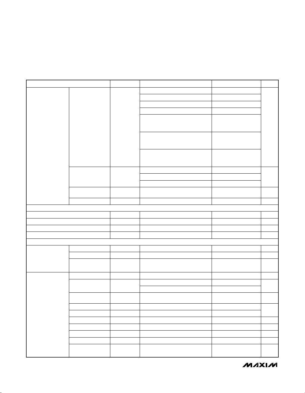
PARAMETER SYMBOL CONDITIONS MIN TYP MAX UNITS
65mA < I
CC(5V)
< 80mA 4. 55 5.00 5.25
I
CC(5V)
< 65mA 4.75 5.00 5.25
I
CC(3V)
< 65mA 2.78 3.00 3.22
I
CC(1.8V)
< 30mA 1.65 1.80 1.95
5V card; current pulses of 40nC
with I < 200mA, t < 400ns,
f < 20 MHz
4.6 5.4
3V card; current pulses of 24nC
with I < 200mA, t < 400ns,
f < 20 MHz
2.75 3.25
Output Low Volt age V
CC2
1.8V card; current pul ses of 12nC
with I < 200mA, t < 400ns,
f < 20 MHz
1.62 1.98
V
V
CC(5V)
= 0 to 5V -80
V
CC(3V)
= 0 to 3V -65
Output Current I
CC2
V
CC(1.8V)
= 0 to 1.8V -30
mA
Shutdown Current
Thresho ld
I
CC(SD)
120 mA
Card-Active Mode
Slew Rate V
CCSR
Up/down; C < 300nF (Note 5) 0.05 0.16 0.22 V/µs
DATA LINES (I/O A ND I/OIN)
I/O I/OIN Fall ing Edge Dela y t
D(IO-IOIN)
200 ns
Pullup Pul se Active T ime t
PU
100 ns
Maximum Frequency f
IOMAX
1 MHz
Input Capacitance C
I
10 pF
I/O, AUX1, AUX2 PIN S
Output Low Volt age V
OL_IO1IOL_IO
= 1mA 0 0.3 V
Output Current I
OL_IO1
V
OL_IO
= 0V 0 -1 mA
Card-Inactive Mode
Internal Pul lup
Res istor
R
PU_IO
To V
CC
9 11 19 k
Output Low Volt age V
OL_IO2IOL_IO
= 1mA 0 0.3 V
I
OH_IO
= < -20µA 0.8 x V
CC
V
CCOutput H igh
Voltage
V
OH_IO2
I
OH_IO
= < -40µA (3V/5V) 0.75 x V
CC
V
CC
V
Output Ri se/Fall
Time
t
OT
CL= 30pF 0.1 µ s
Input Low Voltage V
IL_IO
-0.3 +0.8
Input High Voltage V
IH_IO
1.5 V
CC
V
Input Low Current I
IL_IO
V
IL_IO
= 0V 600 µA
Input High Current I
IH_IO
V
IH_IO
= V
CC
20 µA
Input Ri se/Fa ll Time t
IT
1.2 µ s
Current Lim itation I
IO(LIMIT)CL
= 30pF -15 +15 mA
Card-Active Mode
Current When
Pullup Act ive
I
PU
CL= 80pF, VOH= 0.9 x V
DD
-1 mA
RECOMMENDED DC OPERATING CONDITIONS (continued)
(VDD= +3.3V, V
= +5.0V, TA= +25°C, unless otherwise noted.) (Note 1)
DDA
DS8113
4 _______________________________________________________________________________________
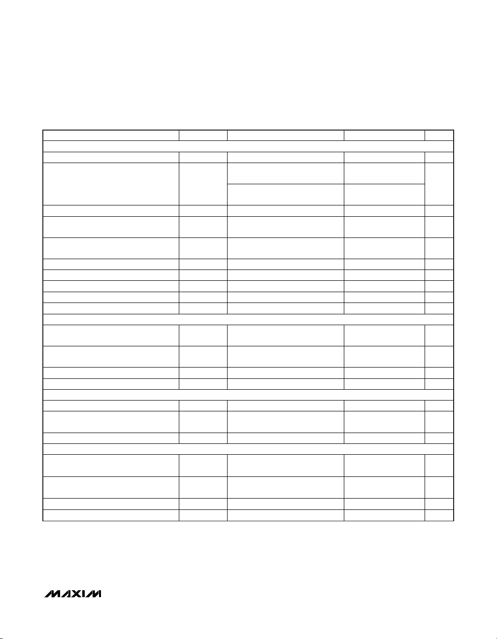
Smart Card Interface
PARAMETER SYMBOL CONDITIONS MIN TYP MAX UNITS
I/OIN, AUX1IN, AUX2IN PIN S
Output Low Volt age V
O
L
I
O
L
= 1mA 0 0.3 V
No Load
0.9 x
V
DD
VDD+
0.1
Output H igh Voltage V
OH
IOH< -40µA
0.75 x
V
DD
VDD+
0.1
V
Output Ri se/Fall T ime t
OT
CL= 30pF, 10% to 90% 0.1 µ s
Input Low Voltage V
I
L
-0.3
0.3 x
V
DD
V
Input High Vo ltage V
IH
0.7 x
V
DD
VDD+
0.3
V
Input Low Current I
IL_IO
VIL= 0V 600 µA
Input High Current I
IH_IO
VIH= V
DD
10 µA
Input R ise/Fal l T ime t
IT
VILto V
IH
1.2 µ s
Integrated Pullup Resistor R
PU
Pullup to V
DD
9 11 13 k
Current When Pullup Act ive I
PU
CL= 30pF, VOH= 0.9 x V
DD
-1 mA
CONTROL PINS (CLKDIV1, CLKDIV2, CMDVCC, RSTIN, 5V/3V, 1_8V)
Input Low Voltage V
IL
-0.3
0.3 x
V
DD
V
Input High Vo ltage V
IH
0.7 x
V
DD
VDD+
0.3
V
Input Low Current I
IL_IO
0 < VIL< V
DD
5 µ A
Input High Current I
IH_IO
0 < VIH< V
DD
5 µ A
INTERRUPT OUTPUT PIN (OFF)
Output Low Volt age V
OL
IOL= 2mA 0 0.3 V
Output H igh Voltage V
OH
IOH= -15µA
0.75 x
V
DD
V
Integrated Pullup Resistor R
PU
Pullup to V
DD
16 20 24 k
PRES, PRES PINS
Input Low Voltage V
IL_PRES
0.3 x
V
DD
V
Input High Vo ltage V
IH_PRES
0.7 x
V
DD
V
Input Low Current I
IL_PRESVIL_PRES
= 0V 40 µA
Input High Current I
IH_PRESVIH_PRES
= V
DD
40 µA
RECOMMENDED DC OPERATING CONDITIONS (continued)
(VDD= +3.3V, V
= +5.0V, TA= +25°C, unless otherwise noted.) (Note 1)
DDA
_______________________________________________________________________________________ 5
DS8113
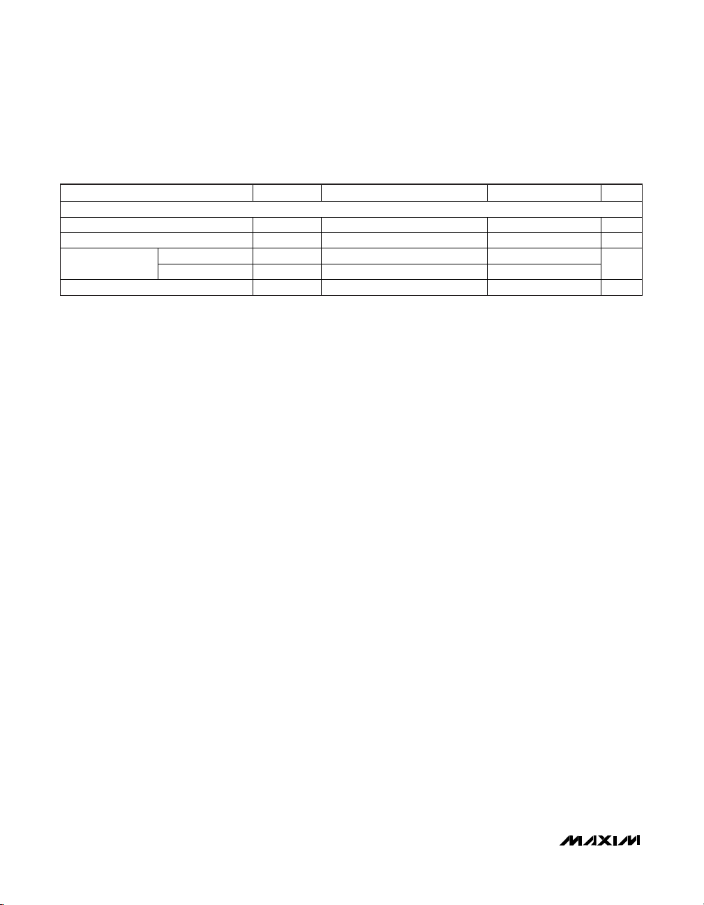
Smart Card Interface
PARAMETER SYMBOL CONDITIONS MIN TYP MAX UNITS
TIMING
A
ctivation T ime t
ACT
5
0 220 µs
Deactivation Time t
D
EACT
50 80 100 µs
Window Start t
3
50 130
CLK to Card Start
Time
Window End t
5
140 220
µs
PRES/PRES Debounce Tim e t
DEBOUNCE
5 8 11 ms
RECOMMENDED DC OPERATING CONDITIONS (continued)
(VDD= +3.3V, V
= +5.0V, TA= +25°C, unless otherwise noted.) (Note 1)
DDA
DS8113
Note 1: Operation guaranteed at -40°C and +85°C but not tested.
Note 2: IDD_IC measures the amount of current used by the DS8113 to provide the smart card current minus the load.
Note 3: Stop mode is enabled by setting CMDVCC, 5V/3V, and 1_8V to a logic-high.
Note 4: Parameters are guaranteed to meet all ISO 7816, GSM11-11, and EMV 2000 requirements. For the 1.8V card, the maximum
rise and fall time is 10ns.
Note 5: Parameter is guaranteed to meet all ISO 7816, GSM11-11, and EMV 2000 requirements. For the 1.8V card, the minimum
slew rate is 0.05V/µs and the maximum slew rate is 0.5V/µs.
6 _______________________________________________________________________________________
 Loading...