Maxim Integrated Producs DS7505, DS7505U+T-R Datasheet
General Description
The DS7505 low-voltage (1.7V to 3.7V) digital thermometer and thermostat provides 9-, 10-, 11-, or 12-bit
digital temperature readings over a -55°C to +125°C
range with ±0.5°C accuracy over a -0°C to +70°C range.
A 9-bit resolution mode is software compatible with the
LM75. Communication with the DS7505 is achieved
through a simple 2-wire serial interface. Three address
pins allow up to eight DS7505 devices to operate on the
same 2-wire bus, which greatly simplifies distributed
temperature-sensing applications.
The DS7505 thermostat has a dedicated open-drain output (O.S.) and programmable fault tolerance, which
allows the user to define the number of consecutive
error conditions that must occur before O.S. is activated.
There are two thermostatic operating modes that control
thermostat operation based on user-defined trip points
(T
OS
and T
HYST
) that are stored in EEPROM registers.
Applications
Networking Equipment
Cellular Base Stations
Office Equipment
Medical Equipment
Any Thermally Sensitive System
Features
♦ Operating Range from 1.7V to 3.7V
♦ Temperature Measurements Require No External
Components
♦ Measures Temperatures from -55°C to +125°C
(-67°F to +257°F)
♦ ±0.5°C Accuracy Over a 0°C to +70°C Range
♦ Thermometer Resolution is User-Configurable
from 9 (Default) to 12 Bits (0.5°C to 0.0625°C
Resolution)
♦ 9-Bit Conversion Time is 25ms (max)
♦ Thermostatic Settings are User-Definable and
Nonvolatile (NV)
♦ Stand-Alone Thermostat Capability
♦ Data Read/Write Occurs Through a 2-Wire Serial
Interface (SDA and SCL Pins)
♦ Data Lines Filtered Internally for Noise Immunity
(50ns Deglitch)
♦ Optional Bus Timeout Feature Prevents Lockup
Problems on 2-Wire Interface
♦ Multidrop Capability Simplifies Distributed
Temperature-Sensing Applications
♦ Pin/Software Compatible with the LM75
♦ Available in 8-Pin SO and µMAX
®
Packages
DS7505
Digital Thermometer and Thermostat
________________________________________________________________
Maxim Integrated Products
1
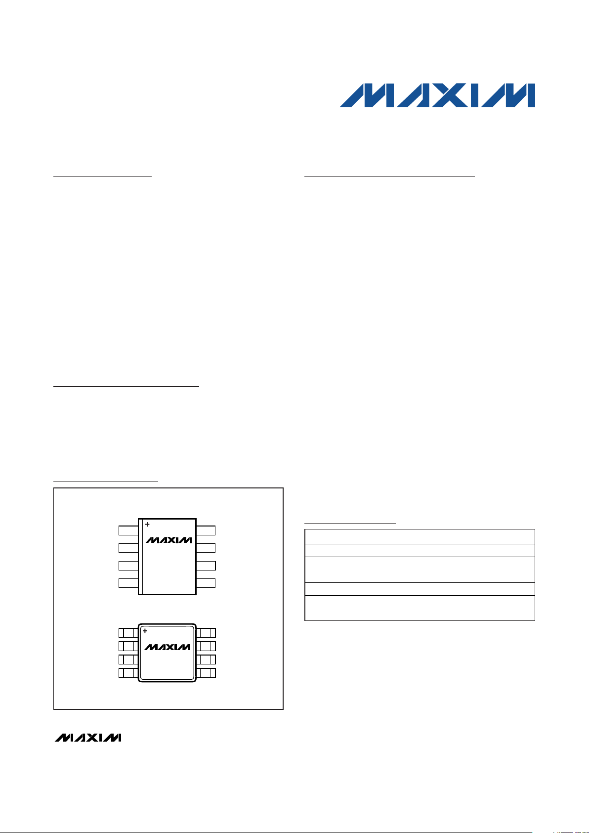
SO
TOP VIEW
27A0SCL
1 8 VDDSDA
A1O.S. 3 6
A2GND
45
DS7505
μ
MAX
27A0SCL
1 8 VDDSDA
A1O.S. 3 6
A2GND 4 5
DS7505
Pin Configurations
Ordering Information
Rev 1; 3/08
For pricing, delivery, and ordering information, please contact Maxim Direct at 1-888-629-4642,
or visit Maxim’s website at www.maxim-ic.com.
PART TEMP RANGE PIN-PACKAGE
DS7505S+ -55°C to +125°C 8 SO (150 mils)
DS7505S+T&R -55°C to +125°C
8 SO (150 mils),
2500-Piece T&R
DS7505U+ -55°C to +125°C 8 μMAX
DS7505U+T&R -55°C to +125°C
8 μMAX,
3000-Piece T&R
+
Denotes a lead-free package.
T&R = Tape and reel.
µMAX is a registered trademark of Maxim Integrated Products, Inc.
Commands are capitalized for clarity.
DS7505
Digital Thermometer and Thermostat
2 _______________________________________________________________________________________
ABSOLUTE MAXIMUM RATINGS
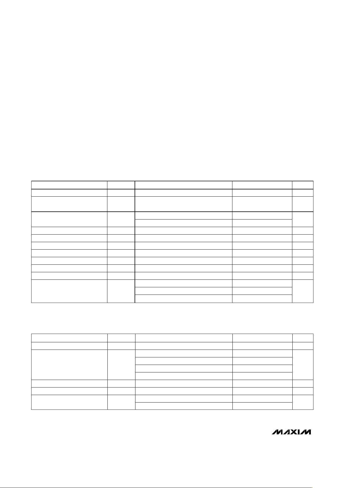
DC ELECTRICAL CHARACTERISTICS
(1.7V ≤ VDD≤ 3.7V, TA= -55°C to +125°C, unless otherwise noted.)
Stresses beyond those listed under “Absolute Maximum Ratings” may cause permanent damage to the device. These are stress ratings only, and functional
operation of the device at these or any other conditions beyond those indicated in the operational sections of the specifications is not implied. Exposure to
absolute maximum rating conditions for extended periods may affect device reliability.
Voltage Range on VDD Relative to Ground ..........-0.3V to +4.0V
Voltage Range on Any Other Pin
Relative to Ground.............................................-0.3V to +6.0V
Operating Temperature Range .........................-55°C to +125°C
Storage Temperature Range .............................-55°C to +125°C
Soldering Temperature...........................Refer to the IPC/JEDEC
J-STD-020 Specification.
PARAMETER SYMBOL CONDITIONS MIN MAX UNITS
Supply Voltage VDD 1.7 3.7 V
Input Voltage Range (SDA, SCL,
O.S., A0, A1, A2)
(Note 1) -0.3 +5.5 V
0°C to +70°C ± 0.5
Thermometer Error
(Note 2, 3)
T
ERR
-55°C to +125°C ± 2.0
°C
Input Logic-High VIH (Note 1) 0.7 × VDD V
Input Logic-Low VIL (Note 1) 0.3 × VDD V
SDA Output Logic-Low Voltage V
OL1
6mA sink current (Note 1) 0 0.6 V
O.S. Saturation Voltage V
OL2
4mA sink current (Notes 1, 2) 0.8 V
Input Current Each I/O pin 0.4V < V
I/O
< 0.9 x VDD -10 +10 μA
I/O Capacitance C
I/O
10 pF
Standby Current I
DD1
(Notes 4, 5, 6) 2 μA
Active temp convers ions 750
Communication only 100
Active Current
(Notes 4, 5, 6)
I
DD
E
2
Copy only 500
μA
AC ELECTRICAL CHARACTERISTICS
(1.7V ≤ VDD≤ 3.7V, TA= -55°C to +125°C, unless otherwise noted.)
PARAMETER SYMBOL CONDITIONS MIN TYP MAX UNITS
Resolution 9 12 Bits
9-bit conversions 25
10-bit con version s 50
11-bit con version s 100
Temperature Conversion Time t
CONVT
12-bit con version s 200
ms
SCL Frequency f
SCL
400 kH z
EEPROM Copy Tim e tWR -40°C to +85°C 10 ms
-40°C TA +85°C (Note 7) 10k 20k
EEPROM Copy Endurance N
EEWR
TA= +25°C (Note 7) 40k 80k
Cycles
DS7505
Digital Thermometer and Thermostat
_______________________________________________________________________________________ 3
Note 1: All voltages are referenced to ground.
Note 2: Internal heating caused by O.S. loading causes the DS7505 to read approximately 0.5°C higher if O.S. is sinking the
max-rated current.
Note 3: Specified in 12-bit conversion mode. Quantization error must be considered when converting in lower resolutions.
Note 4: I
DD
specified with O.S. pin open.
Note 5: I
DD
specified with VDDat 3.0V and SDA, SCL = 3.0V, TA= -55°C to +85°C.
Note 6: I
DD
specified with A0, A1, A2 = 0V or VDD.
Note 7: V
DD
must be > 2.0V.
Note 8: E
2
Copy occurs at +25°C.
Note 9: See the timing diagram (Figure 1). All timing is referenced to 0.9 x V
DD
and 0.1 x VDD.
Note 10: After this period, the first clock pulse is generated.
Note 11: The DS7505 provides an internal hold time of at least 75ns on the SDA signal to bridge the undefined region of SCL’s
falling edge.
Note 12: For example, if C
B
= 300pF, then t
R(MIN)
= t
F(MIN)
= 50ns.
Note 13: This timeout applies only when the DS7505 is holding SDA low. Other devices can hold SDA low indefinitely and the
DS7505 does not reset.
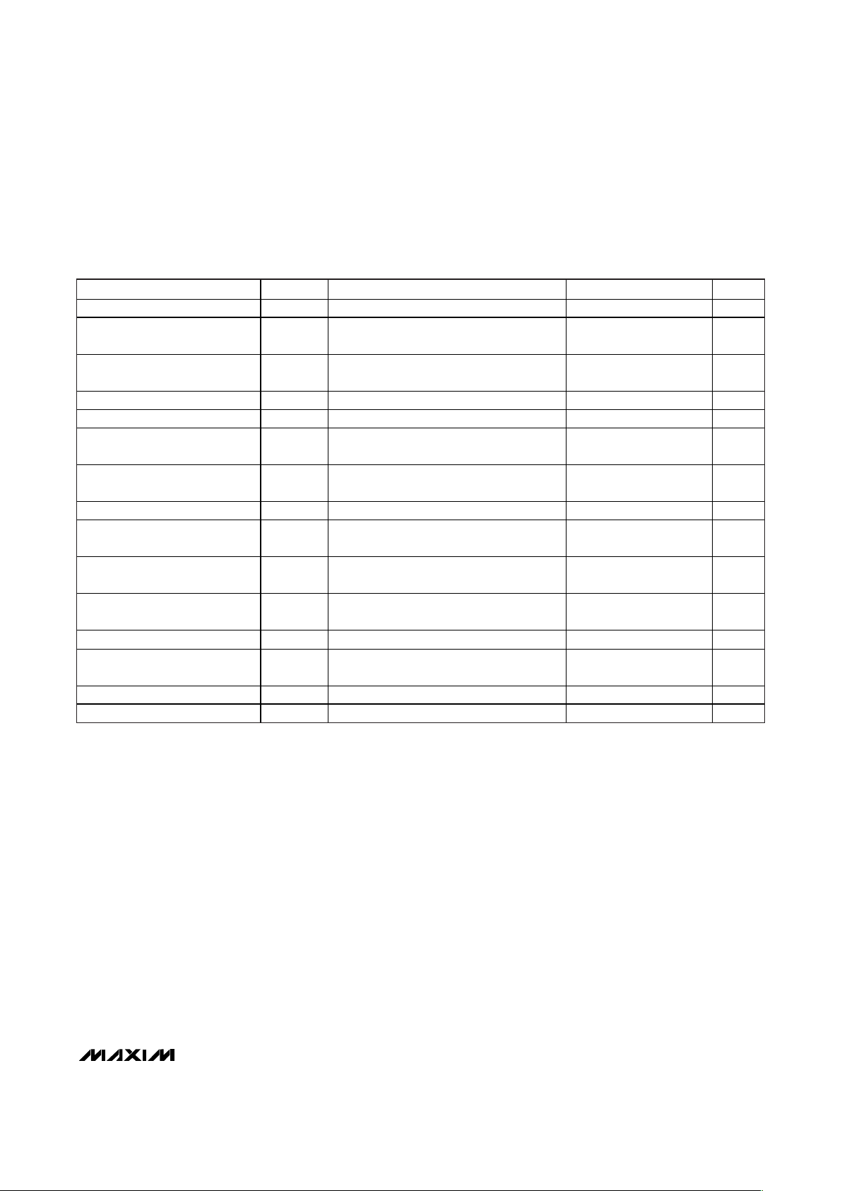
AC ELECTRICAL CHARACTERISTICS (continued)
(1.7V ≤ VDD≤ 3.7V, TA= -55°C to +125°C, unless otherwise noted.)
PARAMETER SYMBOL CONDITIONS MIN TYP MAX UNITS
EEPROM Data Retention t
EEDR
-40°C to +125°C (Note 8) 10 Years
Bus Free Time Between a STOP
and START Condition
t
BUF
(Note 9) 1.3 μs
START and Repeated START
Hold Time from Falling SCL
t
HD: STA
(Notes 9, 10)
600
ns
Low Period of SCL t
LOW
(Note 9) 1.3 μs
High Period of SCL t
HIGH
(Note 9) 0.6 μs
Repeated START Condition
Setup Time to R is ing SCL
t
SU:STA
(Note 9) 600 ns
Data-Out Hold Time from Falling
SCL
t
HD:DAT
(Notes 9, 11) 0 0.9 μs
Data-In Setup Time to Ri sing
t
SU:DAT
(Note 9) 100 ns
Rise T ime of SDA and SCL
(Receive)
t
R
(Notes 9, 12)
20 +
0.1C
B
300
ns
Fall Time of SDA and SCL
(Receive)
t
F
(Notes 9, 12)
20 +
0.1C
B
300 ns
Spike Suppression Filter Time
(Deglitch Filter)
t
SS
0 50 ns
STOP Setup Time to Rising SCL t
SU:STO
(Note 9) 600 ns
Capacitive Load for Each Bus
Line
C
B
400 pF
Input Capacitance CI 5 pF
Serial Interface Reset Time t
TIMEOUT
SDA time low (Note 13) 75 325 m s
DS7505
Digital Thermometer and Thermostat
4 _______________________________________________________________________________________
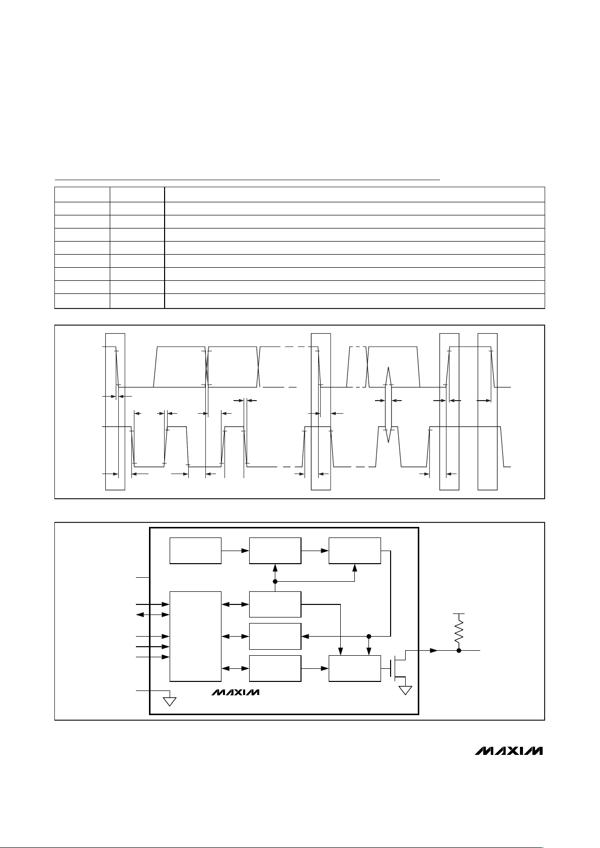
Pin Description
PIN NAME FUNCTION
1 SDA Data Input/Output. For 2-wire serial commun ication port. Open drain.
2 SCL Clock Input. For 2-wire serial communication port.
3 O.S. Thermo stat Output. Open drain.
4 GND Ground
5 A2 Address Input
6 A1 Address Input
7 A0 Address Input
8 VDD Supply Voltage. +1.7V to +3.7V supply pin.
SDA
SCL
SR P S
t
F
t
LOW
t
HD:STA
t
HD:DAT
t
SU:STA
t
SU:STO
t
HD:STA
t
SPtR
t
SU:DAT
t
R
t
F
t
BUF
Figure 1. Timing Diagram
OVERSAMPLING
MODULATOR
DIGITAL
DECIMATOR
PRECISION
REFERENCE
ADDRESS
AND
I/O CONTROL
VDD
CONFIGURATION
REGISTER
TEMPERATURE
REGISTER
SCL
SDA
A0
A1
A2
O.S.
GND
TOS AND T
HYST
REGISTERS
THERMOSTAT
COMPARATOR
DS7505
R
F
Figure 2. Block Diagram
DS7505
Digital Thermometer and Thermostat
_______________________________________________________________________________________ 5
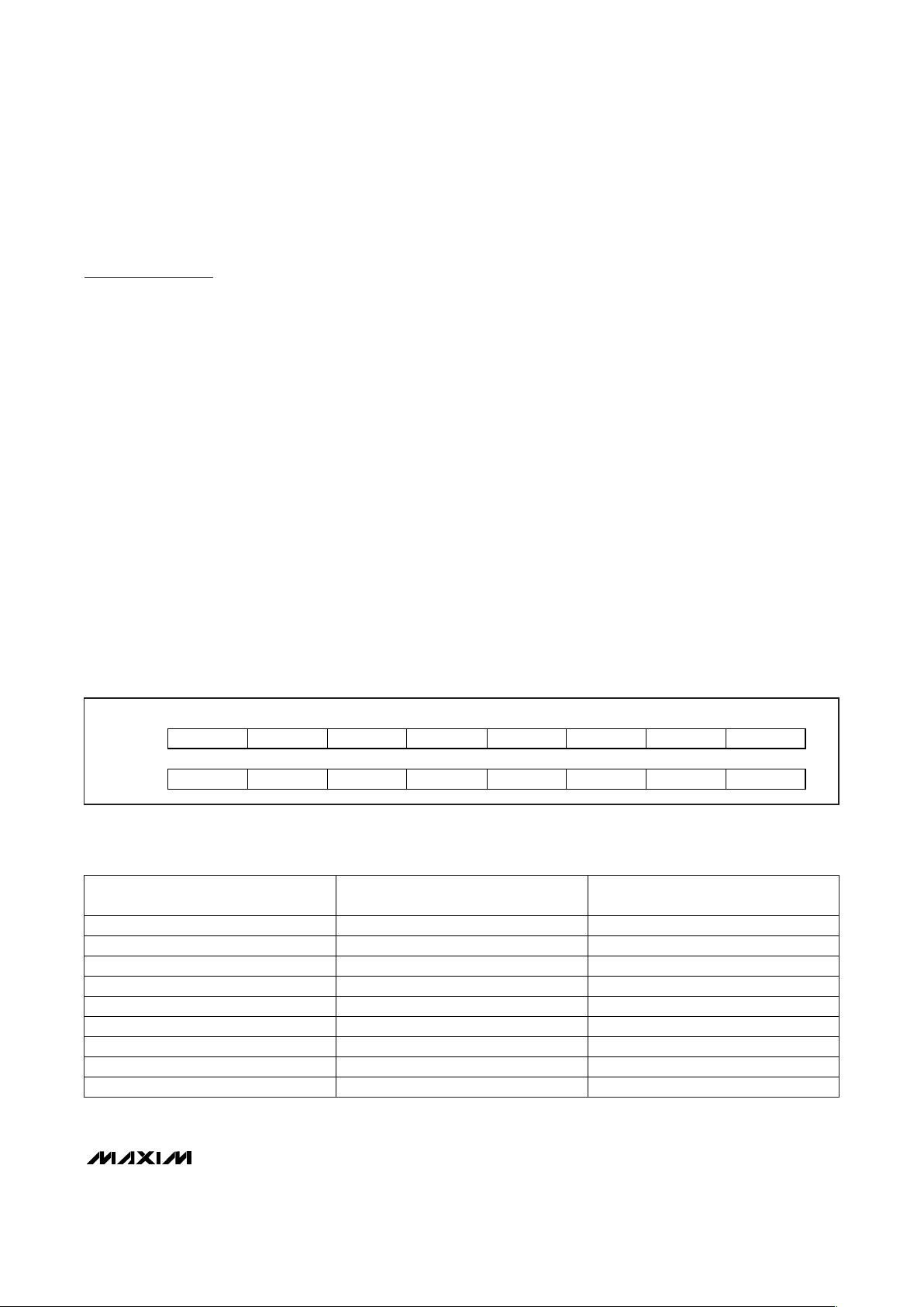
Bit 15 Bit 14 Bit 13 Bit 12 Bit 11 Bit 10 Bit 9 Bit 8
MS Byte S 2
6
2
5
2
4
2
3
2
2
2
1
2
0
Bit 7 Bit 6 Bit 5 Bit 4 Bit 3 Bit 2 Bit 1 Bit 0
LS Byte 2-1 2
-2
2
-3
2
-4
0 0 0 0
Figure 3. Temperature, TOS, and T
HYST
Register Format
Table 1. 12-Bit Resolution Temperature/Data Relationship
Operation⎯Measuring
Temperature
The DS7505 measures temperature using a bandgap
temperature-sensing architecture. An on-board deltasigma analog-to-digital converter (ADC) converts the
measured temperature to a digital value that is calibrated in degrees Celsius; for Fahrenheit applications a
lookup table or conversion routine must be used. The
DS7505 is factory-calibrated and requires no external
components to measure temperature.
The DS7505 can be configured to power up either
automatically converting temperature or in a low-power
standby state. The preferred power-up mode can be
set using the SD bit in the configuration register as
explained in the
Configuration Register
section. The
resolution of the digital output data is user-configurable
to 9, 10, 11, or 12 bits, corresponding to temperature
increments of 0.5°C, 0.25°C, 0.125°C, and 0.0625°C,
respectively. The factory default resolution at power-up
is 9 bits (R1 = 0, R0 = 0), however this can be programmed to 10, 11, or 12 bits using the R0 and R1 bits
in the configuration register as explained in the
Configuration Register
section. Note that the conver-
sion time doubles for each additional bit of resolution.
After each temperature measurement and analog-todigital (A/D) conversion, the DS7505 stores the temperature as a 16-bit two’s complement number in the
2-byte temperature register (see Figure 3). The sign bit
(S) indicates if the temperature is positive or negative:
for positive numbers S = 0 and for negative numbers S
= 1. The most recently converted digital measurement
can be read from the temperature register at any time.
Since temperature conversions are performed in the
background, reading the temperature register does not
affect the operation in progress.
Bits 3 through 0 of the temperature register are hardwired to 0. When the DS7505 is configured for 12-bit
resolution, the 12 MSBs (bits 15 through 4) of the temperature register contain temperature data. For 11-bit
resolution, the 11 MSBs (bits 15 through 5) of the temperature register contain data, and bit 4 reads out as 0.
Likewise, for 10-bit resolution, the 10 MSBs (bits 15
through 6) contain data, and for 9-bit the 9 MSBs (bits
15 through 7) contain data and all unused LSBs contains 0s. Table 1 gives examples of 12-bit resolution digital output data and the corresponding temperatures.
TEMPERATURE (°C)
DIGITAL OUTPUT
(BINARY)
DIGITAL OUTPUT
(HEX)
+125 0111 1101 0000 0000 7D00
+25.0625 0001 1001 0001 0000 1910
+10.125 0000 1010 0010 0000 0A20
+0.5 0000 0000 1000 0000 0080
0 0000 0000 0000 0000 0000
-0.5 1111 1111 1000 0000 FF80
-10.125 1111 0101 1110 0000 F5E0
-25.0625 1110 0110 1111 0000 E6F0
-55 1100 1001 0000 0000 C900
 Loading...