Maxim Integrated Producs DS4412 Datasheet

General Description
The DS4412 contains two I2C adjustable-current DACs
that are each capable of sinking or sourcing current. Each
output has 15 sink and 15 source settings that are programmed by I2C interface. The full-scale range and step
size of each output is determined by an external resistor
that can adjust the output current over a 4:1 range.
The output pins, OUT0 and OUT1, power-up in a highimpedance state.
Applications
Power-Supply Adjustment
Power-Supply Margining
Adjustable Current Sink or Source
Features
♦ Two Current DACs
♦ Full-Scale Current 500µA to 2mA
♦ Full-Scale Range for Each DAC Determined by
External Resistors
♦ 15 Settings Each for Sink and Source Modes
♦ I2C-Compatible Serial Interface
♦ Low Cost
♦ Small Package (8-Pin µSOP)
♦ -40°C to +85°C Temperature Range
♦ 2.7V to 5.5V Operation
DS4412
Dual-Channel, I2C Adjustable
Sink/Source Current DAC
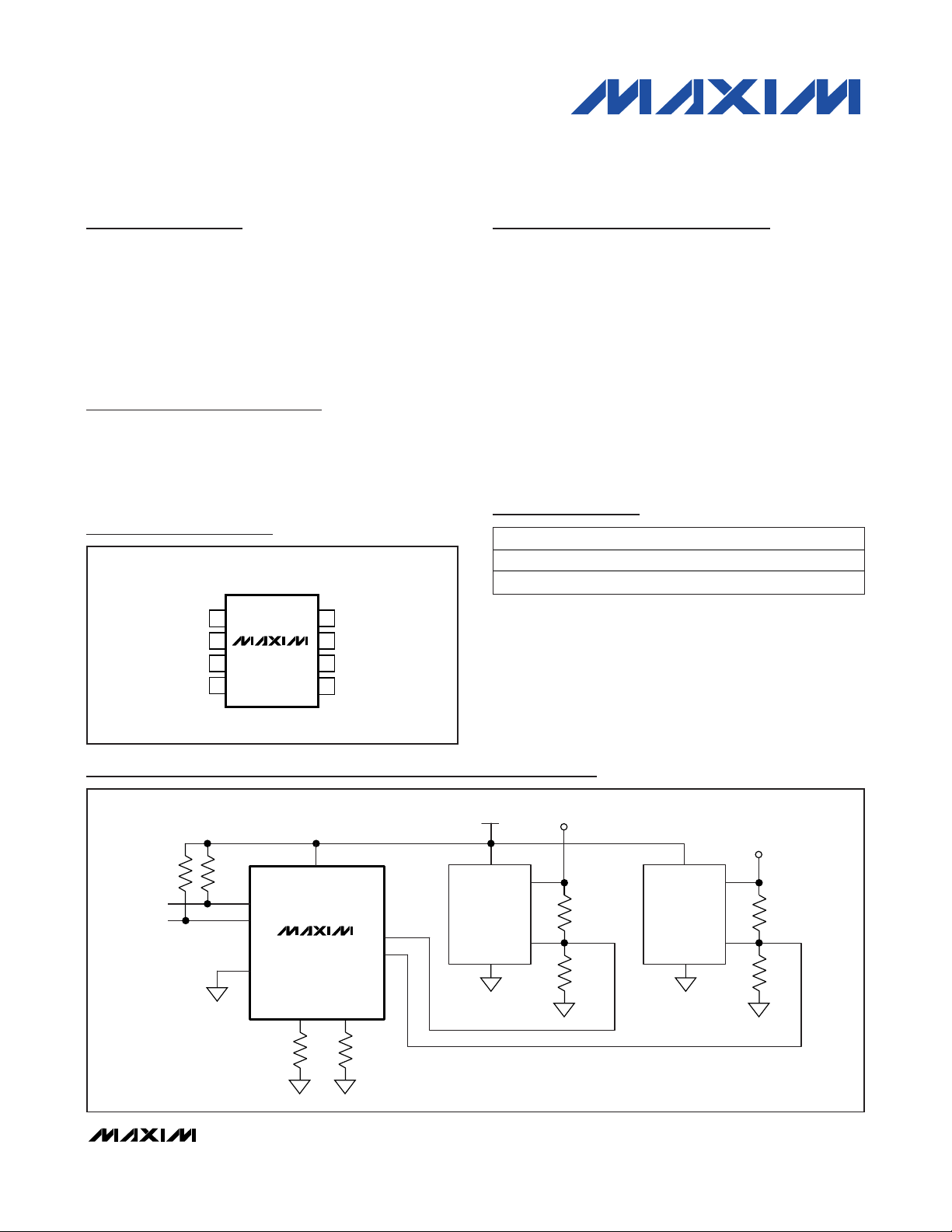
DC-DC
CONVERTER
FB
OUT
SDA
SCL
OUT0
OUT1
GND
R
FS0
R
FS1
4.7kΩ4.7kΩ
V
CC
V
CC
V
OUT0
FS0
FS1
R
0B
R
0A
DC-DC
CONVERTER
FB
OUT
V
OUT1
R
1B
R
1A
DS4412
Typical Operating Circuit
Ordering Information
Rev 0; 9/07
________________________________________________________________
Maxim Integrated Products
1
For pricing, delivery, and ordering information, please contact Maxim Direct at 1-888-629-4642,
or visit Maxim’s website at www.maxim-ic.com.
+
Denotes a lead-free package.
T&R = Tape and reel.
μ
Pin Configuration
TOP VIEW
+
SDA
SCL
FS1
1
2
DS4412
3
4
8
V
CC
7
OUT1
6
OUT0
5
FS0GND
PART TEMP RANGE PIN-PACKAGE
DS4412U+ -40°C to +85°C 8 μSOP
DS4412U+T&R -40°C to +85°C 8 μSOP
SOP

DS4412
Dual-Channel, I2C Adjustable
Sink/Source Current DAC
2 _______________________________________________________________________________________
ABSOLUTE MAXIMUM RATINGS
RECOMMENDED OPERATING CONDITIONS
(TA= -40°C to +85°C)
Stresses beyond those listed under “Absolute Maximum Ratings” may cause permanent damage to the device. These are stress ratings only, and functional
operation of the device at these or any other conditions beyond those indicated in the operational sections of the specifications is not implied. Exposure to
absolute maximum rating conditions for extended periods may affect device reliability.
Voltage Range on VCC, SDA, and SCL
Relative to Ground.............................................-0.5V to +6.0V
Voltage Range on OUT0, OUT1 Relative to
Ground ................-0.5V to (V
CC
+ 0.5V) (Not to exceed 6.0V.)
Operating Temperature Range ...........................-40°C to +85°C
Storage Temperature Range .............................-55°C to +125°C
Soldering Temperature .....................................Refer to IPC/JEDEC
J-STD-020 Specification
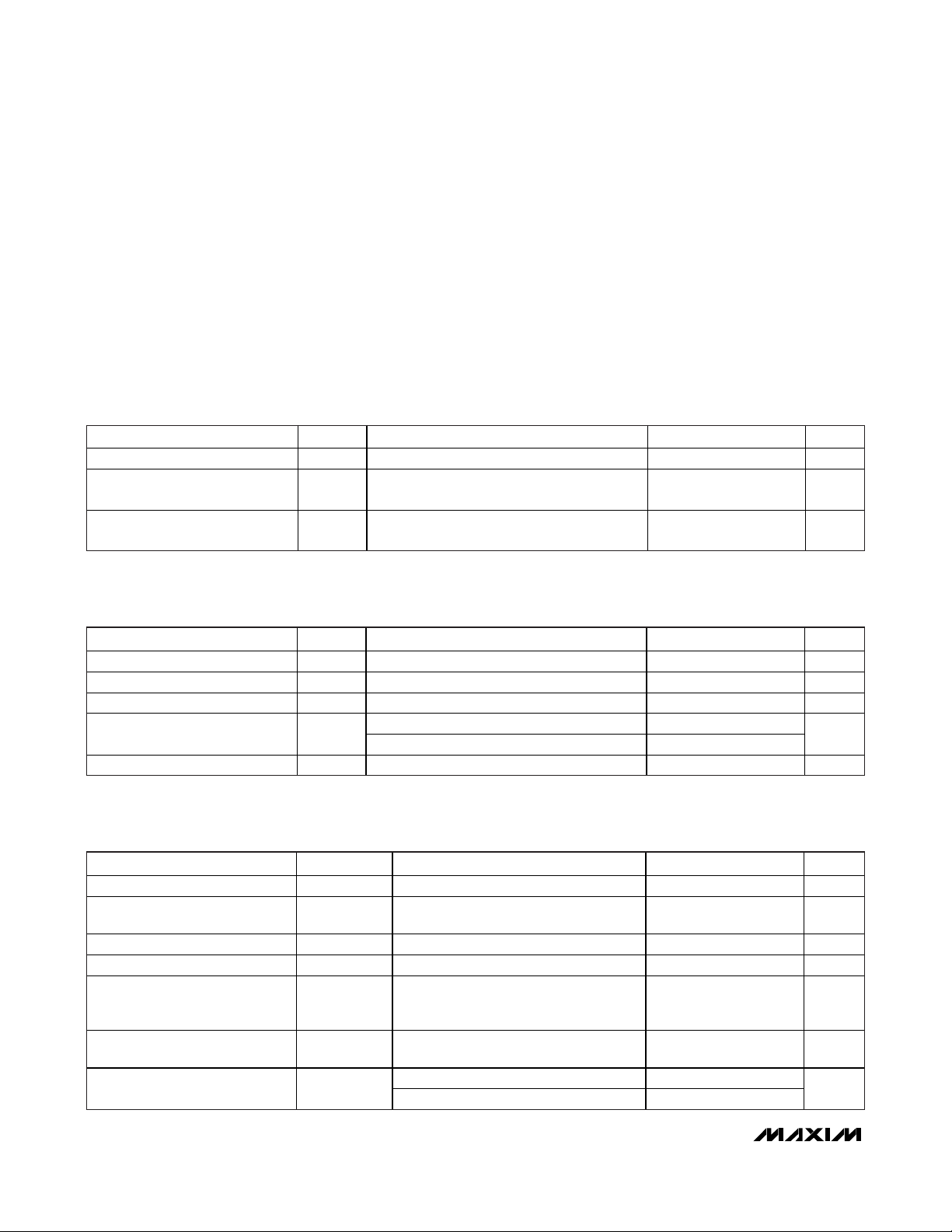
DC ELECTRICAL CHARACTERISTICS
(VCC= +2.7V to +5.5V, TA= -40°C to +85°C.)
OUTPUT CURRENT CHARACTERISTICS
(VCC= +2.7V to +5.5V, TA= -40°C to +85°C.)
Supply Voltage V
Input Logic 1 (SDA, SCL) V
Input Logic 0 (SDA, SCL) V
PARAMETER SYMBOL CONDITIONS MIN TYP MAX UNITS
(Note 1) 2.7 5.5 V
CC
IH
IL
Supply Current ICC VCC = 5.5V (Note 2) 500 μA
Input Leakage (SDA, SCL) IIL VCC = 5.5V 1 μA
Output Leakage (SDA) IL 1 μA
Output Current Low (SDA) I
RFS Voltage V
PARAMETER S YMBOL CONDITIONS MIN TYP MAX UNITS
VOL = 0.4V 3
OL
VOL = 0.6V 6
0.607 V
RFS
0.7 x
V
CC
-0.3
VCC +
0.3
0.3 x
V
CC
V
V
mA
Output Voltage for Sink ing
Output Voltage for Sourcing
Current
Ful l-Scale Sink Output Current I
Ful l-Scale Source Output Current I
Output-Current Full-Scale
Accuracy
Output-Current Temperature
Coefficient
Output-Current Variation due to
Power-Supply Change
PARAMETER S YMBOL CONDITIONS MIN TYP MAX UNITS
V
OUT:SINK
V
OUT:SOURCE
OUT:SINK
OUT:SOURCE
I
OUT:FS
I
OUT:TC
VCC > V
(Note 3) 0
(Note 3) 0.5 2.0 mA
(Note 3) -2.0 -0.5 mA
+25°C, VCC = 4.0V; using 0.1% R
resi stor (Note 4)
V
(Note 5) ±75 ppm/°C
DC source +0.36
DC sin k +0.12
OUT0
OUT:SINK
= V
(Note 3) 0.5 3.5 V
FS
= 1.2V
OUT1
V
-
CC
0.75
±6 %
V
%/V

DS4412
Dual-Channel, I2C Adjustable
Sink/Source Current DAC
_______________________________________________________________________________________ 3
Note 1: All voltages with respect to ground, currents entering the IC are specified positive and currents exiting the IC are negative.
Note 2: Supply current specified with all outputs set to zero current setting with all inputs driven to well-defined logic levels. SDA and
SCL are connected to V
CC
. Excludes current through R
FS
resistors (I
RFS
). Total current includes ICC+ 2.5 x (I
RFS0
+ I
RFS0
).
Note 3: The output voltage range must be satisfied to ensure the device meets its accuracy and linearity specifications.
Note 4: Input resistors R
FS
must be between 2.25kΩ and 9.0kΩ to ensure the device meets its accuracy and linearity specifications.
Note 5: Temperature drift excludes drift caused by external resistor.
Note 6: Differential linearity is defined as the difference between the expected incremental current increase with respect to position
and the actual increase. The expected incremental increase is the full-scale range divided by 15.
Note 7: Integral linearity is defined as the difference between the expected value as a function of the setting and the actual value.
The expected value is a straight line between the zero and the full-scale values proportional to the setting.
Note 8: Timing shown is for fast-mode (400kHz) operation. This device is also backward compatible with I
2
C standard-mode timing.
Note 9: C
B
—total capacitance of one bus line in pF.
OUTPUT CURRENT CHARACTERISTICS (continued)
(VCC= +2.7V to +5.5V, TA= -40°C to +85°C.)
I2C AC ELECTRICAL CHARACTERISTICS
(VCC= +2.7V to +5.5V, TA= -40°C to +85°C.)
Output-Current Variation due to
Output Voltage Change
Output Leakage Current at Zero
Current Setting
Output-Current Differential
Linearity
Output-Current Integral Linear ity INL (Note 7) 1 LSB
PARAMETER S YMBOL CONDITIONS MIN TYP MAX UNITS
DC source, V
DC sin k, V
-1 +1 μA
I
ZERO
DNL (Note 6) 0.5 LSB
measured at 1.2V -0.02
OUT
measured at 1.2V +0.12
OUT
SCL Clock Frequency f
Bus Free Time Between STOP
and START Conditions
Hold Time (Repeated) START
Condition
Low Period of SCL t
High Period of SCL t
Data Hold Time t
Data Setup Time t
START Setup Time t
SDA and SCL Rise Time t
SDA and SCL Fall Time t
STOP Setup Time t
SDA and SCL Capacitive Loading C
PARAMETER SYMBOL CONDITIONS MIN TYP MAX UNITS
SCL
t
BUF
t
HD:STA
LOW
HIGH
DH:DAT
SU:DAT
SU:STA
R
F
SU:STO
B
(Note 8) 0 400 kHz
1.3 µs
0.6 µs
1.3 µs
0.6 µs
0 0.9 µs
100 ns
0.6 µs
(Note 9)
(Note 9)
(Note 9) 400 pF
20 +
0.1C
B
20 +
0.1C
B
0.6 µs
300 ns
300 ns
%/V
 Loading...