General Description
The DS4026 is a temperature-compensated crystal
oscillator (TCXO) that provides ±1ppm frequency stability over the -40°C to +85°C industrial temperature
range. Each device is factory calibrated over temperature to achieve the ±1ppm frequency stability. Standard
frequencies for the device include 12.8, 19.44, 20.0,
38.88, 40.0, and 51.84MHz. Contact the factory for custom frequencies.
The DS4026 provides excellent phase-noise characteristics. The output is a push-pull CMOS square wave with
symmetrical rise and fall times. In addition, the DS4026 is
designed to provide a maximum frequency deviation of
less than ±4.6ppm over 10 years. The device also provides an I2C interface to allow pushing and pulling of the
output frequency by a minimum of ±8ppm (±5ppm for
10MHz) with typical 1ppb resolution.
The DS4026 implements a temperature-to-voltage conversion with a nonlinear relationship. The output from the
temperature-to-voltage converter is used to drive the voltage-controlled crystal oscillator to compensate for frequency change.
The device implements an on-chip temperature sensor
lookup table, and a digital-to-analog converter (DAC) to
adjust the frequency. An I2C interface used to communicate with the DS4026 performs temperature readings and
frequency push-pull.
Applications
Reference Clock Generation Wireless
Telecom/Datacom/SATCOM Test and Measurement
Features
o ±1ppm Frequency Accuracy Over -40°C to +85°C
o Standard Frequencies: 12.8, 19.44, 20.0, 38.88,
40.0, 51.84MHz
o Maximum ±4.6ppm Deviation Over 10 Years
o Minimum ±8ppm (±5ppm for 10MHz) Digital
Frequency Tuning Through I2C Interface
o Surface-Mount 16-Pin SO Package
o Pb Free/RoHS Compliant
DS4026
10MHz to 51.84MHz TCXO
______________________________________________
Maxim Integrated Products
1
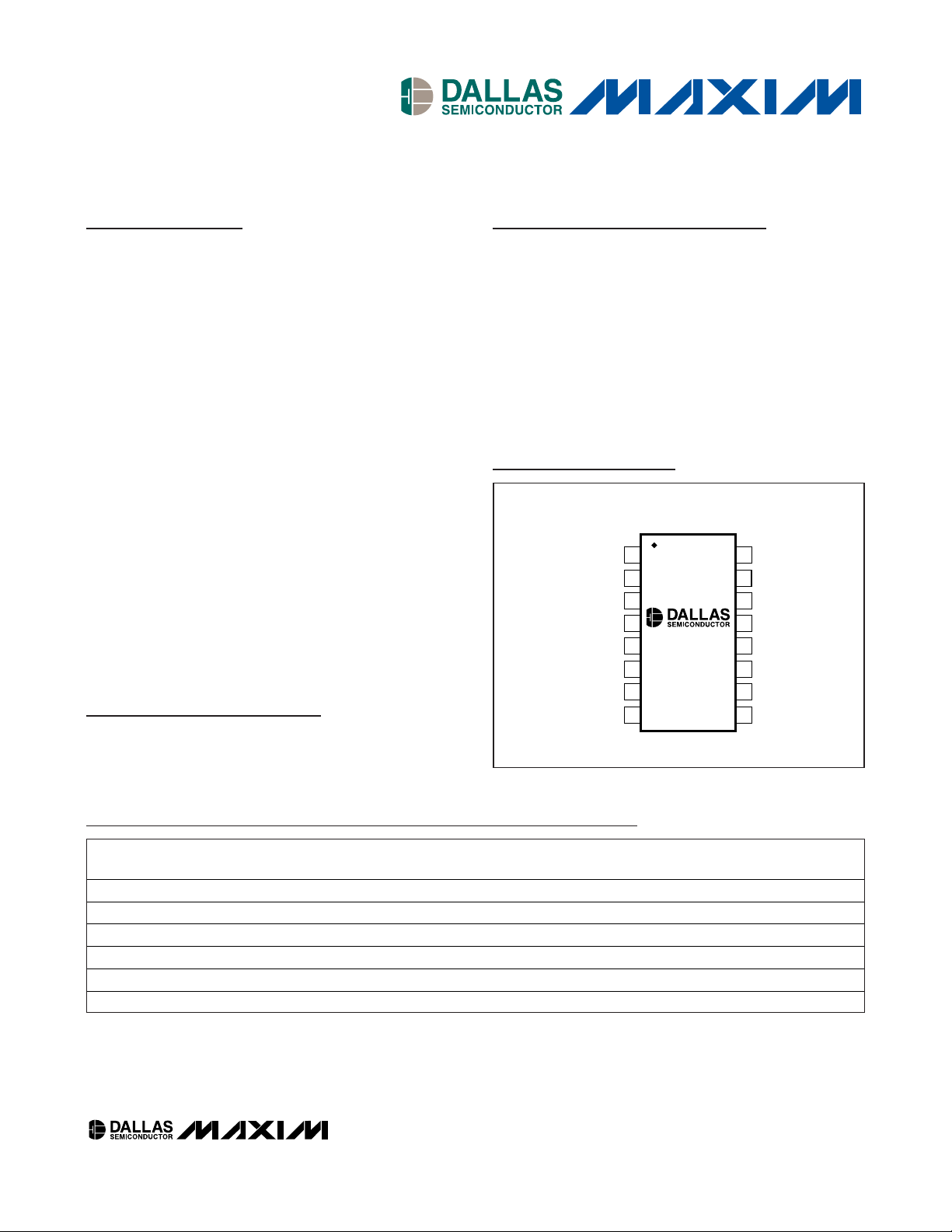
Pin Configuration
Rev 1; 9/07
For pricing, delivery, and ordering information, please contact Maxim Direct at 1-888-629-4642,
or visit Maxim’s website at www.maxim-ic.com.
+
Denotes a lead-free package.
*
The top mark will include a “+” for a lead-free/RoHS-compliant device.
Ordering Information continued at end of data sheet.
Ordering Information
TOP VIEW
GNDA
V
REF
V
V
OSC
GNDOSC
N.C.
N.C.
N.C.
1
2
3
CC
4
DS4026
5
6
7
8
SO
16
V
CCD
15
FOUT
14
GNDD
13
SCL
12
SDA
GND
11
10
N.C.
9
N.C.
PART TEMP RANGE
DS4026S+BCC
DS4026S+BCN -40°C to +85°C 12.8 16 SO DS4026-BCN
DS4026S+HCC 0°C to +70°C 19.44 16 SO DS4026-HCC
DS4026S+HCN -40°C to +85°C 19.44 16 SO DS4026-HCN
DS4026S+JCC 0°C to +70°C 20.0 16 SO DS4026-JCC
DS4026S+JCN -40°C to +85°C 20.0 16 SO DS4026-JCN
0°C to +70°C 12.8 16 SO DS4026-BCC
OUTPUT (f
(MHz, CMOS)
NOM
)
PIN-PACKAGE TOP MARK*

DS4026
10MHz to 51.84MHz TCXO
2 _____________________________________________________________________
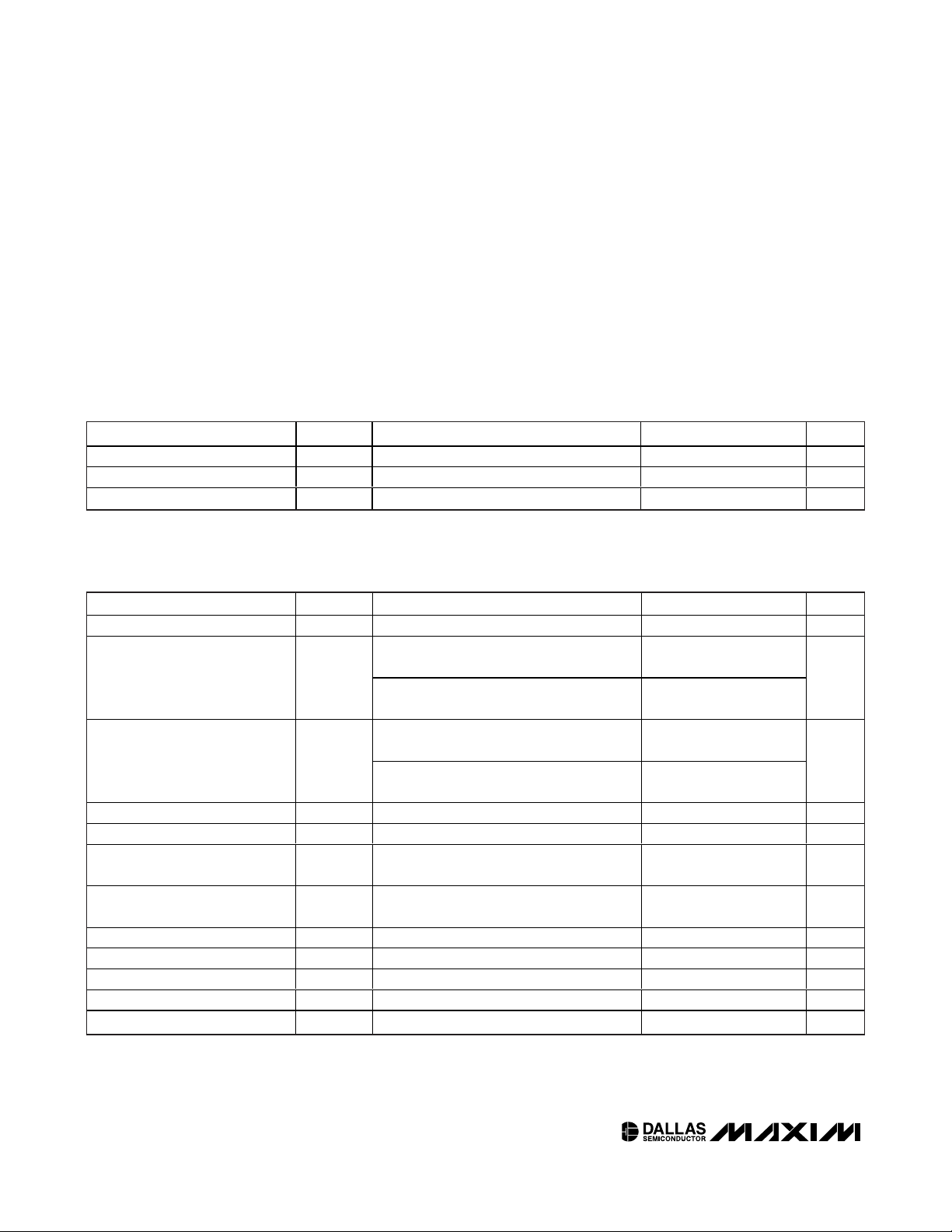
ABSOLUTE MAXIMUM RATINGS
RECOMMENDED DC OPERATING CONDITIONS
(TA= -40°C to +85°C, unless otherwise noted.)
Stresses beyond those listed under “Absolute Maximum Ratings” may cause permanent damage to the device. These are stress ratings only, and functional
operation of the device at these or any other conditions beyond those indicated in the operational sections of the specifications is not implied. Exposure to
absolute maximum rating conditions for extended periods may affect device reliability.
Voltage Range on V
CC
,
V
CCD
, and V
OSC
Relative to Ground..............................................-0.3V to +3.8V
Voltage Range on SDA, SCL, and FOUT
Relative to Ground...................................-0.3V to (V
CC
+ 0.3V)
Operating Temperature Range (noncondensing)....-40°C to +85°C
Storage Temperature Range .............................-55°C to +125°C
Soldering Temperature………………………….See IPC/JEDEC
J-STD-020 Specification
DC ELECTRICAL CHARACTERISTICS (Note 1)
(VCC= 3.135V to 3.465V, TA= -40°C to +85°C, unless otherwise noted.) (Notes 2, 3)
PARAMETER SYMBOL CONDITIONS MIN TYP MAX UNITS
Power-Supply Voltage V
Oscillator Power Supply V
Driver Power Supply V
CC
OSC
CCD
VCC Active-Supply Current I
V
OSC
Current
V
CCD
Current
SCL Input Leakage I
SDA Leakage I
SCL, SDA High Input Voltage V
SCL, SDA Low Input Voltage V
SDA Logic 0 Output I
FOUT High Output Voltage V
FOUT Low Output Voltage V
FOUT Rise/Fall Time tR/t
FOUT Duty Cycle t
PARAMETER SYMBOL CONDITIONS MIN TYP MAX UNITS
CC
(Note 4) 1.5 2.5 mA
FOUT CMOS output on, CL = 10pF,
Oscillator Active-Supply
I
OSC
frequency < 25MHz
FOUT CMOS output on, CL = 10pF,
frequency ≥ 25MHz
FOUT CMOS output on, CL = 10pF,
Driver Active-Supply
I
CCD
frequency < 25MHz
FOUT CMOS output on, CL = 10pF,
frequency ≥ 25MHz
LI
LO
OL
OH
OL
Output off -1 +1 µA
IH
IL
VCC = 3.0V, VOL = 0.4V 3 mA
V
= 3V, IOH = -2mA 2.4 V
CCD
V
= 3V, IOL = 2.0mA 0.4 V
CCD
(0.1 x V
F
D
0.5 x V
CCD
CCD
3.135 3.3 3.465 V
3.135 3.3 3.465 V
3.135 3.3 3.465 V
34
59
23
35
-1 +1 µA
) - (0.9 x V
0.7 x
V
CC
-0.3
)2ns
CCD
V
CC
+ 0.3
+0.3 x
V
CC
(Note 5) 45 55 %
mA
mA
V
V

DS4026
10MHz to 51.84MHz TCXO
_____________________________________________________________________ 3
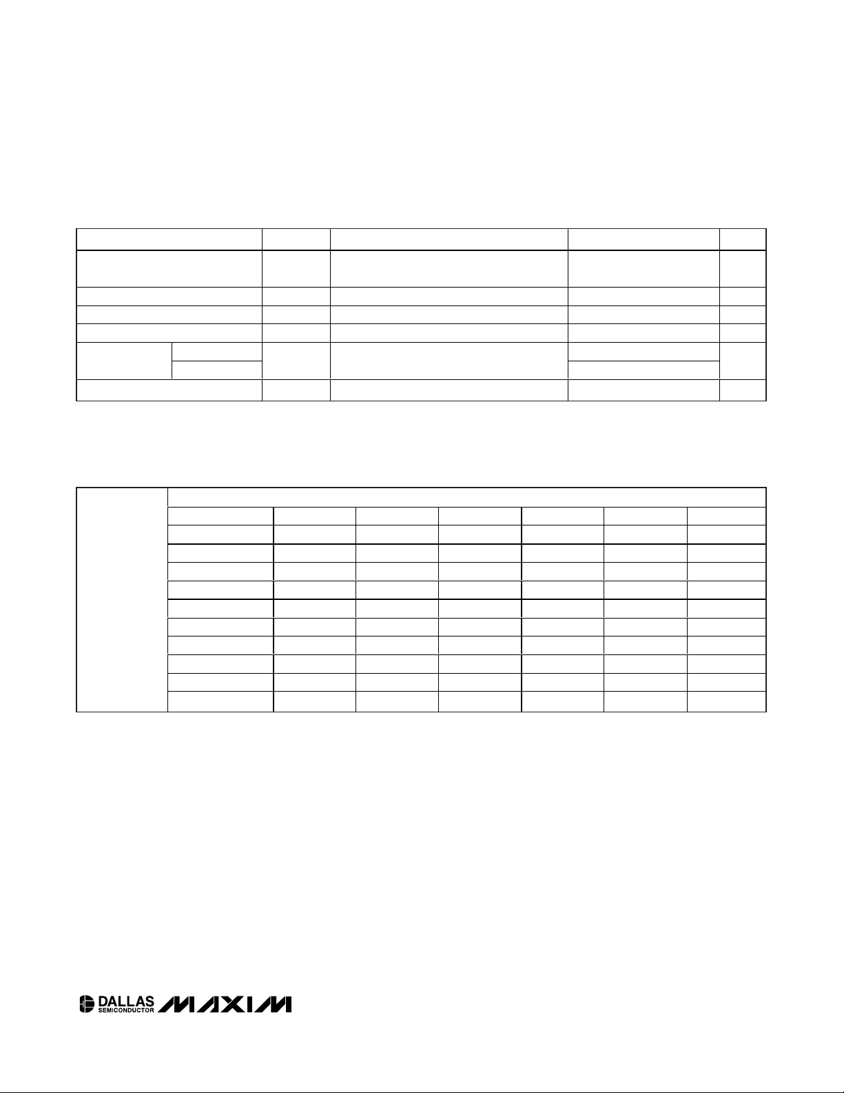
AC ELECTRICAL CHARACTERISTICS (Note 1)
(VCC= 3.135V to 3.465V, TA= -40°C to +85°C, unless otherwise noted.)
PHASE NOISE
PARAMETER SYMBOL CONDITIONS MIN TYP MAX UNITS
Frequency Stability vs.
Temperature
Frequency Stability vs. Voltage Δf1/V CL = 10pF to ground, +25°C -2 +2 ppm/V
Aging, First Year Δf1/Yr (Note 5) -1 +1 ppm
Aging, Years 2–15 Δf1/Yr (Note 5) -2 +2 ppm
Frequency Pull
Range
Frequency Pull Resolution Δf
Except 10MHz ±8 ±15
10MHz
Δf
1/TA
Δf
RES
CL = 10pF to ground
FTU N E H = 3Fh and FTU N E L = FFh;
FTU N E H = 40h and FTU N E L = 00h at + 25° C
f
NOM
– 1ppm
±5 ±10
f
NOM
f
NOM
+ 1ppm
1 ppb
ppm
ppm
PHASE NOISE (dBc/Hz) (TYPICAL, +25°C, 3.3V)
OFFSET (MHz) 10Hz 100Hz 1kHz 10kHz 100kHz 1MHz
12.80 -88.41 -130.16 -147.84 -150.84 -151.71 -151.87
19.44 -82.63 -125.12 -145.03 -146.87 -151.69 -151.52
20.00 -83.71 -120.76 -145.44 -150.96 -151.18 -151.45
CARRIER
FREQUENCY
38.88 -79.01 -120.06 -141.75 -150.59 -152.50 -153.06
40.00 -80.80 -115.44 -141.17 -151.59 -152.37 -153.00
51.84 -74.09 -120.39 -142.33 -151.14 -153.21 -153.94
10.0 -92.52 -134.83 -147.22 -150.84 -151.25 -150.84
16.384 -87.44 -128.53 -147.67 -150.78 -152.72 -151.75
16.8 -89.6 -126.20 -146.88 -151.90 -152.28 -151.93
24.0 -83.98 -119.45 -143.08 -150.33 -150.34 -150.67

DS4026
10MHz to 51.84MHz TCXO
4 _____________________________________________________________________
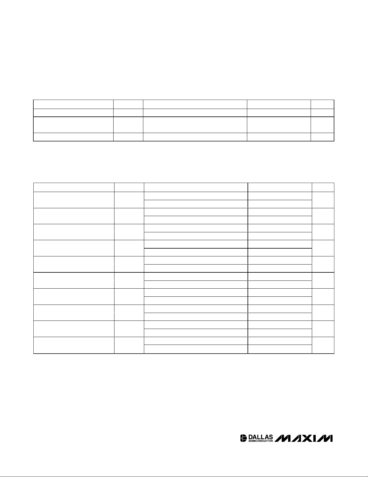
TEMPERATURE SENSOR ELECTRICAL CHARACTERISTICS (Note 1)
(VCC= 3.135V to 3.465V, TA= -40°C to +85°C, unless otherwise noted.)
AC ELECTRICAL CHARACTERISTICS
(VCC= 3.135V to 3.465V, TA= -40°C to +85°C, unless otherwise noted.) (Note 2)
PARAMETER S YMBOL CONDITIONS MIN TYP MAX UNITS
Temperature Sensor Accuracy T -3 +3 °C
Temperature Sensor Convers ion
Time
Temperature Sensor Resolution N2 12 Bits
PARAMETER SYMBOL CONDITIONS MIN TYP MAX UNITS
SCL Clock Frequency f
Bus Free Time Between STOP
and START Conditions
Hold Time (Repeated) START
Condition (Note 6)
Low Period of SCL Clock t
High Period of SCL Clock t
Data Hold Time
(Notes 7, 8)
Data Setup Time (Note 9) t
Start Setup Time t
Rise Time of Both SDA and SCL
Signals (Note 10)
Fall Time of Both SDA and SCL
Signals (Note 10)
t
11 ms
CONVT
SCL
t
BUF
t
HD:STA
LOW
HIGH
t
HD:DAT
SU:DAT
SU:STA
t
t
Standard mode 0 100
Fast mode 100 400
Standard mode 4.7
Fast mode 1.3
Standard mode 4.0
Fast mode 0.6
Standard mode 4.7
Fast mode 1.3
Standard mode 4.0
Fast mode 0.6
Standard mode 0 0.9
Fast mode 0 0.9
Standard mode 250
Fast mode 100
Standard mode 4.7
Fast mode 0.6
Standard mode 20 + 0.1C
R
Fast mode 20 + 0.1C
Standard mode 20 + 0.1C
F
Fast mode 20 + 0.1C
B
B
B
B
1000
300
300
300
kHz
µs
µs
µs
µs
µs
ns
µs
ns
ns
 Loading...