Maxim Integrated Producs DS2710 Datasheet

General Description
The DS2710 is ideal for in-system charging of single-cell
nickel metal hydride (NiMH) cells for low-current
portable applications. Inputs to the DS2710 include USB
voltage sources and 5V regulated adapters.
Temperature, voltage, and charge time are monitored to
provide proper fast-charging control algorithms for
single-cell NiMH or nickel cadmium (NiCd) batteries.
The DS2710 includes battery tests to detect defective or
inappropriate cells such as alkaline primary batteries.
Applications
Small Rechargeable Devices
Voice Recorders
Cordless Mouse
Battery-Powered Toys
Features
♦ Charges Single-Cell NiMH Cells
♦ Switch-Mode Topologies Supported by Hysteretic
Control Technique
♦ Precharges Deeply Depleted Cells
♦ Fast-Charges NiMH with -ΔV Termination
Sensitivity of 2mV (typ)
♦ Monitors Voltage, Temperature, and Time for
Safety and Secondary Termination
♦ Regulates Charge Current
♦ Designed for External pMOS
♦ Rail-to-Rail MOSFET Driver
♦ Tiny 10-Pin TDFN Package (3mm x 4mm)
DS2710
Single-Cell NiMH Charger
________________________________________________________________
Maxim Integrated Products
1
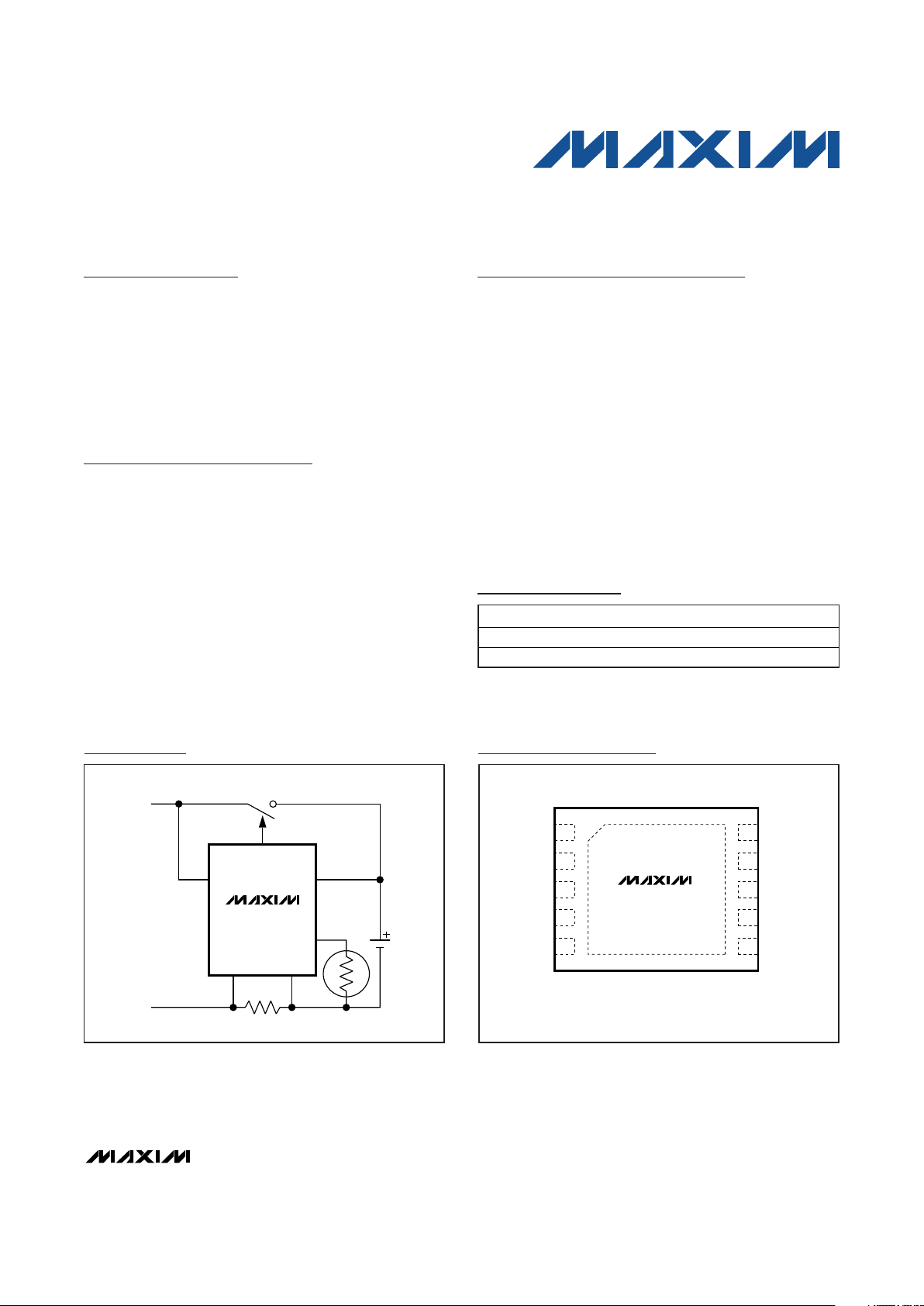
DS2710
110
VP1V
SS
3 8 VN0V
DD
2 9 VN1CS
4 7 TMRTHM
5 6 CTESTSTATUS
TDFN
(3mm × 4mm)
TOP VIEW
+
*EP
*EXPOSED PAD.
Pin Configuration
Ordering Information
DS2710
V
DD
VP1
THM
CS
VN0 VN1
SENSE
CHARGE
SOURCE
NiMH
CELL
GROUND
Typical Operating Circuit
Rev 0; 4/08
For pricing, delivery, and ordering information, please contact Maxim Direct at 1-888-629-4642,
or visit Maxim’s website at www.maxim-ic.com.
+
Denotes a lead-free/RoHS-compliant package.
T&R = Tape and reel.
*
EP = Exposed pad.
PART PIN-PACKAGE
DS2710G+ 10 TDFN-EP*
DS2710G+T& R 10 TDFN-EP*

DS2710
Single-Cell NiMH Charger
2 _______________________________________________________________________________________2 _______________________________________________________________________________________
ABSOLUTE MAXIMUM RATINGS
RECOMMENDED DC OPERATING CONDITIONS
(4.0V ≤ VDD≤ 5.5V, TA= -20°C to +70°C.)
Stresses beyond those listed under “Absolute Maximum Ratings” may cause permanent damage to the device. These are stress ratings only, and functional
operation of the device at these or any other conditions beyond those indicated in the operational sections of the specifications is not implied. Exposure to
absolute maximum rating conditions for extended periods may affect device reliability.
Voltage Range on All Pins Relative to VSS............-0.3V to +6.0V
Continuous Source/Sink Current CS ...................................20mA
Continuous Source Current STATUS ..................................10mA
Operating Temperature Range ...........................-40°C to +85°C
Storage Temperature Range .............................-55°C to +125°C
Soldering Temperature...........................Refer to the IPC/JEDEC
J-STD-020 Specification.
PARAMETER SYMBOL CONDITIONS MIN TYP MAX UNITS
Supply Voltage VDD (Note 1) 4.0 5.5 V
Input Voltage Range CTEST, TMR, THM, VP1, VN1 -0.3 VDD V
DC ELECTRICAL CHARACTERISTICS
(4.0V ≤ VDD≤ 5.5V, TA= -20°C to +70°C, unless otherwise noted.)
PARAMETER SYMBOL CONDITIONS MIN TYP MAX UNITS
Supply Current, VDD I
DD
Operating mode (Note 2) 250 1000 μA
UVLO Threshold V
UVLO
VDD rising (Note 1) 3.5 3.9 V
UVLO Hysteresis V
UHYS
VDD falling from above V
UVLO
30 mV
Output-Voltage Low, CS V
OL1
VDD = 5.0V, IOL = +20mA (Note 1) 1.0 V
Output-Voltage High, CS V
OH1
VDD = 5.0V, IOL = -20mA (Note 1) 4.0 V
Output-Voltage Low, STATUS V
OL2
VDD = 5.0V, IOL = +2mA (Notes 1, 3) 0.50 V
Output-Voltage High, STATUS V
OH2
VDD = 5.0V, IOH = -2mA (Notes 1, 3) 4.0 V
Threshold Voltage,
-V Termination
V
-V
After t
THO
(Note 4) 1.0 2.0 3.0 mV
125 mV
Current-Sense Reference
Voltage
V
IREF
(Notes 1, 5)
-6 +6 %
Hysteres is, Current-Sense
Comparator
V
HYS-
COMP
Centered ~ 0.113V 18 23 27 mV
Propagation Time, Current-Sense
Comparator to Dri ver Output
t
PDLY
2mV overdrive/underdrive at trip thresho ld
(Notes 4, 6)
0.1 μs
CS Pin Pul lup Current ICS VDD < V
UVLO
(Note 4) 2 10 μA
STATUS Pin Pulldown Current I
STAT
VDD < V
UVLO
(Note 4) 2 10 μA
Depleted Cell Voltage Thresho ld V
LOW
VP1 - VN1 0.9 1.0 1.1 V
Overcharge Voltage Threshold
V
MAX-
OPEN
VP1 - VN1, CS = high (Note 7) 1.55 1.65 1.75 V
Open Socket Voltage Threshold
V
MAX-
CHARGE
VP1 - VN1, CS = low (Note 7) 1.64 1.75 1.86 V
Offset, V
MAX-O PEN
- V
MAX-CHARGE
VOS (Note 7) 98 100 102 mV

DS2710
Single-Cell NiMH Charger
_______________________________________________________________________________________ 3
Note 1: Voltages relative to VSS.
Note 2: Specification does not include CS and STATUS pin currents.
Note 3: STATUS pin is active high.
Note 4: Specification is guaranteed by design.
Note 5: Specification applicable during charge cycle with T
A
= 0°C to +70°C.
Note 6: 50mV overdrive while connected to a pMOS transistor (such as ZXM62P02 from Zetex).
Note 7: V
BAT-MAX1
and V
BAT-MAX1
ranges never overlap.
Note 8: VT
HM-MIN
, V
THM-MAX
, and V
THM-STOP
are fixed ratios of VDD. Their ranges never overlap.
Note 9: Maximum allowable leakage on TMR to maintain SUSPEND state.
DC ELECTRICAL CHARACTERISTICS (continued)
(4.0V ≤ VDD≤ 5.5V, TA= -20°C to +70°C, unless otherwise noted.)
PARAMETER SYMBOL CONDITIONS MIN TYP MAX UNITS
Cold Temperature Detect
Threshold
V
THM-MIN
(Notes 1, 5, 8) 0.73 V
DD
Hot Temperature No-Start
Threshold
V
THM-MAX
(Notes 1, 5, 8) 0.30 0.33 0.36 V
DD
Hot Temperature Safety
Shutdown Threshold
V
THM-ST OP
(Notes 1, 5, 8) 0.29 V
DD
SUSPEND Current Threshold I
SUSP END
(Note 9) 0.1 0.5 μA
Presence-Test Current, VP1 VDD 4.0V 1.0 10 15 μA
Reverse-Leakage Current, VP1 V
DD
= 0V, VP1 = 1.5V 2 μA
Impedance-Voltage Test Range V
CTEST
32 400 mV
ELECTRICAL CHARACTERISTICS: TIMING
(4.0V ≤ VDD≤ 5.5V, TA= -20°C to +70°C, unless otherwise noted.)
PARAMETER SYMBOL CONDITIONS MIN TYP MAX UNITS
Internal Time-Base Period t
BASE
0.96 Seconds
Internal Time-Base Accuracy -10 +10 %
DF1 FAST-CHARGE 96.9
DF2 PRECHARGE/TOP-OFF 25.0
CS Output Duty Factor
DF3 MAINTENANCE 1.56
%
CELL TEST Interval t
CTST
31 Seconds
PRECHARGE Timeout t
PCHG
V
CELL
< V
LOW
34 Minutes
FAST-CHARGE Termination
Hold-Off Period
t
THO
4 Minutes
FAST-CHARGE Flat Voltage
Timeout
t
FLAT
V
CELL
not increasing 16 Minutes
Charge-Timer Period t
CTMR
R
TMR
= 40k 1.0 Hours
Charge-Timer Accuracy R
TMR
= 40k -6 +6 %
Charge-Timer Range t
CTMR -R ANGE
0.5 5.0 Hours
Toggle Rate, Charging f
CHARGE
1 Hz
Toggle Rate, FAULT State f
FAULT
4 Hz

DS2710
Single-Cell NiMH Charger
4 _______________________________________________________________________________________
Pin Description
PIN NAME FUNCTION
1 VSS Device Ground. Connect s directly to the negative terminal of the charge source.
2 CS Charge Source. Feedback control for switching circuitry.
3 V
DD
Power-Supply Input. Connects to the posit ive terminal of the charge source through a decoupling
network.
4 THM Thermistor Input. Connects to a thermistor located near the cell and a resistor-div ider from the VDD pin.
5 STATUS Status Output. Drives an external LED or microprocessor input to indicate charge status.
6 CTEST Impedance Test. Connects to VSS through an external resistor to set the impedance-test threshold.
7 TMR Fast-Charge Timer. Connects to VSS through an external res istor to set the fast-charge timeout period.
8 VN0 Current-Sense Negative Input. Connects to the charge source s ide of the external sense resistor.
9 VN1 Current-Sense Positive Input. Connects to the cell side of the external sense resistor.
10 VP1 Cel l Voltage Sense. The voltage of the cel l is monitored through thi s input pin.
— EP Exposed Pad. Connects to VSS.
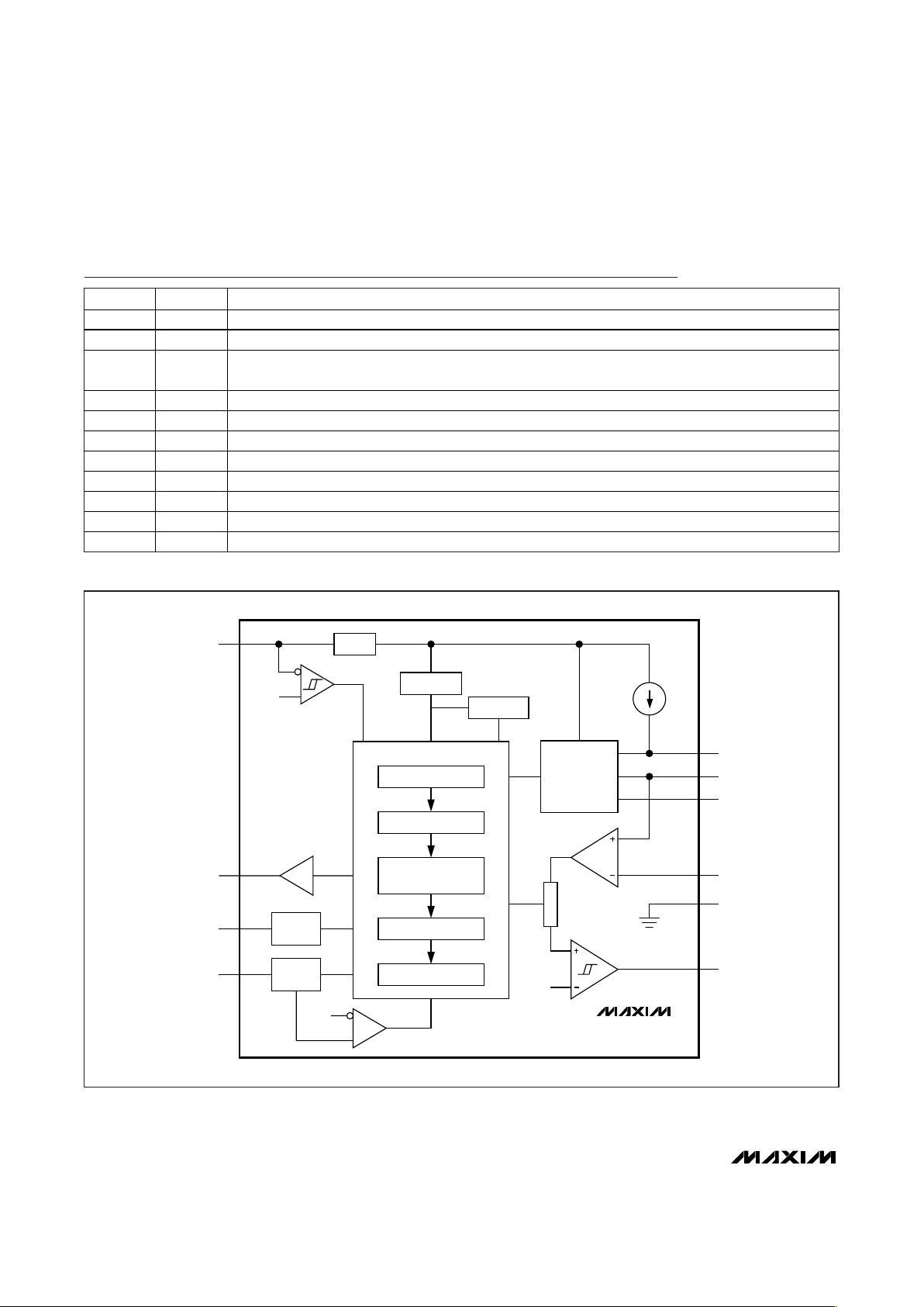
DS2710
BIAS
OSCILLATOR
WATCHDOG
ABORT
VP1
I
PTST
UVLO
3.5V
V
DD
STATUS
CTEST
STATUS
MAINTENANCE CHARGE
TOP-OFF CHARGE
SUSPEND
PRECHARGE
PRESENSE TEST
STATE MACHINE
FAST-CHARGE AND
CELL TESTS
VOLTAGE
AND
TEMPERATURE
MEASUREMENT
DUTYFACTOR
CONTROL
VN1
THM
CS
0.125V
0.1μA
V
SS
VN0
CELL
TEST
TMR
CHARGE
TIMER
Figure 1. Block Diagram
 Loading...