1 of 286
REV: 022007
Note: Some revisions of this device may incorporate deviations from published specifications known as errata. Multiple revisions of any device
may be simultaneously available through various sales channels. For information about device errata, click here: www.maxim-ic.com/errata
.
DS26518
8-Port T1/E1/J1 Transceive
r
GENERAL DESCRIPTION
The DS26518 is a single-chip 8-port framer and line
interface unit (LIU) combination for T1, E1, and J1
applications. Each port is independently configurable,
supporting both long-haul and short-haul lines. The
8-port SCT is software compatible with the DS26519
and nearly software compatible with the DS26528
and its derivatives.
APPLICATIONS
Routers
Channel Service Units (CSUs)
Data Service Units (DSUs)
Muxes
Switches
Channel Banks
T1/E1 Test Equipment
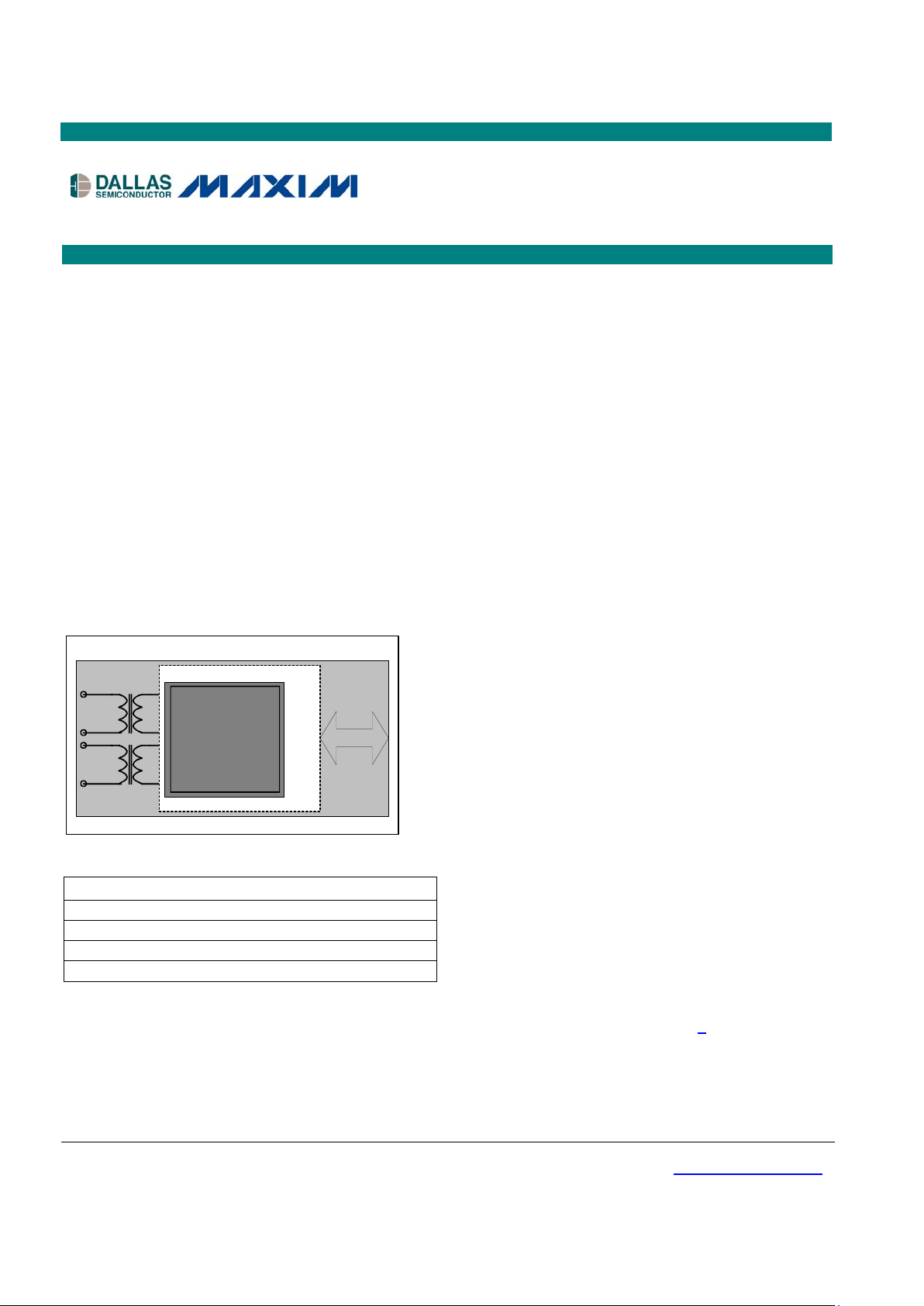
FUNCTIONAL DIAGRAM
DS26518
T1/J1/E1
Transceiver
T1/E1/J1
NETWORK
BACKPLANE
TDM
x8
ORDERING INFORMATION
PART TEMP RANGE PIN-PACKAGE
DS26518G
0°C to +70°C
256 TE-CSBGA
DS26518G+
0°C to +70°C
256 TE-CSBGA
DS26518GN
-40°C to +85°C
256 TE-CSBGA
DS26518GN+
-40°C to +85°C
256 TE-CSBGA
+ Denotes lead-free/RoHS compliant device.
FEATURES
Eight Complete T1, E1, or J1 Long-Haul/
Short-Haul Transceivers (LIU Plus Framer)
Independent T1, E1, or J1 Selections for Each
Transceiver
Fully Internal Impedance Match, No External
Resistor
Software-Selectable Transmit- and Receive-
Side Termination for 100Ω T1 Twisted Pair,
110Ω J1 Twisted Pair, 120Ω E1 Twisted Pair,
and 75Ω E1 Coaxial Applications
Hitless Protection Switching
Crystal-Less Jitter Attenuators Can Be
Selected for Transmit or Receive Path; Jitter
Attenuator Meets ETS CTR 12/13, ITU-T
G.736, G.742, G.823, and AT&T Pub 62411
External Master Clock Can Be Multiple of
2.048MHz or 1.544MHz for T1/J1 or E1
Operation; This Clock is Internally Adapted
for T1 or E1 Usage in the Host Mode
Receive-Signal Level Indication from -2.5dB
to -36dB in T1 Mode and -2.5dB to -44dB in E1
Mode in Approximate 2.5dB Increments
Transmit Open- and Short-Circuit Detection
LIU LOS in Accordance with G.775, ETS 300
233, and T1.231
Transmit Synchronizer
Flexible Signaling Extraction and Insertion
Using Either the System Interface or
Microprocessor Port
Alarm Detection and Insertion
T1 Framing Formats of D4, SLC-96, and ESF
J1 Support
E1 G.704 and CRC-4 Multiframe
T1-to-E1 Conversion
Features Continued in Section 2.
www.maxim-ic.com

DS26518 8-Port T1/E1/J1 Transceiver
2 of 286
TABLE OF CONTENTS
1. DETAILED DESCRIPTION.................................................................................................9
2. FEATURE HIGHLIGHTS..................................................................................................10
2.1 GENERAL......................................................................................................................................10
2.2 LINE INTERFACE............................................................................................................................10
2.3 CLOCK SYNTHESIZERS ..................................................................................................................10
2.4 JITTER ATTENUATOR.....................................................................................................................10
2.5 FRAMER/FORMATTER....................................................................................................................11
2.6 SYSTEM INTERFACE ......................................................................................................................11
2.7 HDCL CONTROLLERS ...................................................................................................................12
2.8 TEST AND DIAGNOSTICS................................................................................................................12
2.9 MICROCONTROLLER PARALLEL PORT.............................................................................................12
2.10 SLAVE SERIAL PERIPHERAL INTERFACE (SPI) FEATURES ............................................................12
3. APPLICATIONS ...............................................................................................................13
4. SPECIFICATIONS COMPLIANCE...................................................................................14
5. ACRONYMS AND GLOSSARY .......................................................................................16
6. MAJOR OPERATING MODES .........................................................................................17
7. BLOCK DIAGRAMS......................................................................................................... 18
8. PIN DESCRIPTIONS ........................................................................................................20
8.1 PIN FUNCTIONAL DESCRIPTION......................................................................................................20
9. FUNCTIONAL DESCRIPTION .........................................................................................28
9.1 PROCESSOR INTERFACE................................................................................................................28
9.1.1 SPI Serial Port Mode............................................................................................................................ 28
9.1.2 SPI Functional Timing Diagrams ......................................................................................................... 28
9.2 CLOCK STRUCTURE.......................................................................................................................31
9.2.1 Backplane Clock Generation ............................................................................................................... 31
9.2.2 CLKO Output Clock Generation........................................................................................................... 32
9.3 RESETS AND POWER-DOWN MODES..............................................................................................33
9.4 INITIALIZATION AND CONFIGURATION..............................................................................................34
9.4.1 Example Device Initialization and Sequence.......................................................................................34
9.5 GLOBAL RESOURCES ....................................................................................................................34
9.6 PER-PORT RESOURCES ................................................................................................................34
9.7 DEVICE INTERRUPTS .....................................................................................................................34
9.8 SYSTEM BACKPLANE INTERFACE ...................................................................................................36
9.8.1 Elastic Stores....................................................................................................................................... 36
9.8.2 IBO Multiplexing................................................................................................................................... 39
9.8.3 H.100 (CT Bus) Compatibility .............................................................................................................. 45
9.8.4 Transmit and Receive Channel Blocking Registers............................................................................. 47
9.8.5 Transmit Fractional Support (Gapped Clock Mode)............................................................................ 47
9.8.6 Receive Fractional Support (Gapped Clock Mode)............................................................................. 47
9.9 FRAMERS......................................................................................................................................48
9.9.1 T1 Framing...........................................................................................................................................48
9.9.2 E1 Framing........................................................................................................................................... 51
9.9.3 T1 Transmit Synchronizer.................................................................................................................... 53
9.9.4 Signaling .............................................................................................................................................. 54
9.9.5 T1 Data Link.........................................................................................................................................59
9.9.6 E1 Data Link......................................................................................................................................... 61
9.9.7 Maintenance and Alarms..................................................................................................................... 62

DS26518 8-Port T1/E1/J1 Transceiver
3 of 286
9.9.8 Alarms.................................................................................................................................................. 65
9.9.9 Error Count Registers .......................................................................................................................... 67
9.9.10 DS0 Monitoring Function...................................................................................................................... 69
9.9.11 Transmit Per-Channel Idle Code Generation ...................................................................................... 70
9.9.12 Receive Per-Channel Idle Code Insertion............................................................................................ 70
9.9.13 Per-Channel Loopback ........................................................................................................................ 70
9.9.14 E1 G.706 Intermediate CRC-4 Updating (E1 Mode Only)................................................................... 70
9.9.15 T1 Programmable In-Band Loop Code Generator............................................................................... 71
9.9.16 T1 Programmable In-Band Loop Code Detection................................................................................ 72
9.9.17 Framer Payload Loopbacks................................................................................................................. 73
9.10 HDLC CONTROLLERS................................................................................................................74
9.10.1 Receive HDLC Controller.....................................................................................................................74
9.10.2 Transmit HDLC Controller.................................................................................................................... 77
9.11 POWER-SUPPLY DECOUPLING....................................................................................................79
9.12 LINE INTERFACE UNITS (LIUS)....................................................................................................80
9.12.1 LIU Operation.......................................................................................................................................82
9.12.2 Transmitter........................................................................................................................................... 83
9.12.3 Receiver............................................................................................................................................... 86
9.12.4 Hitless Protection Switching (HPS)......................................................................................................90
9.12.5 Jitter Attenuator....................................................................................................................................91
9.12.6 LIU Loopbacks..................................................................................................................................... 92
9.13 BIT ERROR-RATE TEST FUNCTION (BERT).................................................................................95
9.13.1 BERT Repetitive Pattern Set ............................................................................................................... 96
9.13.2 BERT Error Counter............................................................................................................................. 96
10. DEVICE REGISTERS.......................................................................................................97
10.1 REGISTER LISTINGS ...................................................................................................................97
10.1.1 Global Register List.............................................................................................................................. 98
10.1.2 Framer Register List............................................................................................................................. 99
10.1.3 LIU and BERT Register List...............................................................................................................106
10.2 REGISTER BIT MAPS ................................................................................................................107
10.2.1 Global Register Bit Map..................................................................................................................... 107
10.2.2 Framer Register Bit Map.................................................................................................................... 108
10.2.3 LIU Register Bit Map.......................................................................................................................... 117
10.2.4 BERT Register Bit Map......................................................................................................................118
10.3 GLOBAL REGISTER DEFINITIONS...............................................................................................119
10.4 FRAMER REGISTER DESCRIPTIONS...........................................................................................133
10.4.1 Receive Register Descriptions........................................................................................................... 133
10.4.2 Transmit Register Descriptions..........................................................................................................191
10.5 LIU REGISTER DEFINITIONS .....................................................................................................227
10.6 BERT REGISTER DEFINITIONS .................................................................................................237
11. FUNCTIONAL TIMING ...................................................................................................245
11.1 T1 RECEIVER FUNCTIONAL TIMING DIAGRAMS ..........................................................................245
11.2 T1 TRANSMITTER FUNCTIONAL TIMING DIAGRAMS ....................................................................250
11.3 E1 RECEIVER FUNCTIONAL TIMING DIAGRAMS..........................................................................255
11.4 E1 TRANSMITTER FUNCTIONAL TIMING DIAGRAMS ....................................................................259
12. OPERATING PARAMETERS.........................................................................................264
12.1 THERMAL CHARACTERISTICS....................................................................................................265
12.2 LINE INTERFACE CHARACTERISTICS..........................................................................................265
13. AC TIMING CHARACTERISTICS..................................................................................266
13.1 MICROPROCESSOR BUS AC CHARACTERISTICS........................................................................266
13.1.1 SPI Bus Mode.................................................................................................................................... 266
13.2 JTAG INTERFACE TIMING.........................................................................................................277
14. JTAG BOUNDARY SCAN AND TEST ACCESS PORT................................................278

DS26518 8-Port T1/E1/J1 Transceiver
4 of 286
14.1 TAP CONTROLLER STATE MACHINE.........................................................................................279
14.1.1 Test-Logic-Reset................................................................................................................................ 279
14.1.2 Run-Test-Idle ..................................................................................................................................... 279
14.1.3 Select-DR-Scan ................................................................................................................................. 279
14.1.4 Capture-DR........................................................................................................................................ 279
14.1.5 Shift-DR.............................................................................................................................................. 279
14.1.6 Exit1-DR.............................................................................................................................................279
14.1.7 Pause-DR........................................................................................................................................... 279
14.1.8 Exit2-DR.............................................................................................................................................279
14.1.9 Update-DR......................................................................................................................................... 279
14.1.10 Select-IR-Scan ............................................................................................................................... 279
14.1.11 Capture-IR...................................................................................................................................... 280
14.1.12 Shift-IR............................................................................................................................................ 280
14.1.13 Exit1-IR...........................................................................................................................................280
14.1.14 Pause-IR......................................................................................................................................... 280
14.1.15 Exit2-IR...........................................................................................................................................280
14.1.16 Update-IR....................................................................................................................................... 280
14.2 INSTRUCTION REGISTER...........................................................................................................282
14.2.1 SAMPLE:PRELOAD .......................................................................................................................... 282
14.2.2 BYPASS.............................................................................................................................................282
14.2.3 EXTEST ............................................................................................................................................. 282
14.2.4 CLAMP...............................................................................................................................................282
14.2.5 HIGHZ................................................................................................................................................ 282
14.2.6 IDCODE............................................................................................................................................. 282
14.3 JTAG ID CODES......................................................................................................................283
14.4 TEST REGISTERS.....................................................................................................................283
14.4.1 Boundary Scan Register.................................................................................................................... 283
14.4.2 Bypass Register................................................................................................................................. 283
14.4.3 Identification Register......................................................................................................................... 283
15. PIN CONFIGURATION...................................................................................................284
15.1 PIN CONFIGURATION—256-BALL TE-CSBGA ..........................................................................284
16. PACKAGE INFORMATION............................................................................................285
16.1 256-BALL TE-CSBGA (56-G6028-001)...................................................................................285
17. DOCUMENT REVISION HISTORY ................................................................................286

DS26518 8-Port T1/E1/J1 Transceiver
5 of 286
LIST OF FIGURES
Figure 7-1. Block Diagram......................................................................................................................................... 18
Figure 7-2. Detailed Block Diagram........................................................................................................................... 19
Figure 9-1. SPI Serial Port Access for Read Mode, SPI_CPOL = 0, SPI_CPHA = 0............................................... 29
Figure 9-2. SPI Serial Port Access for Read Mode, SPI_CPOL = 1, SPI_CPHA = 0............................................... 29
Figure 9-3. SPI Serial Port Access for Read Mode, SPI_CPOL = 0, SPI_CPHA = 1............................................... 29
Figure 9-4. SPI Serial Port Access for Read Mode, SPI_CPOL = 1, SPI_CPHA = 1............................................... 29
Figure 9-5. SPI Serial Port Access for Write Mode, SPI_CPOL = 0, SPI_CPHA = 0 ............................................... 30
Figure 9-6. SPI Serial Port Access for Write Mode, SPI_CPOL = 1, SPI_CPHA = 0 ............................................... 30
Figure 9-7. SPI Serial Port Access for Write Mode, SPI_CPOL = 0, SPI_CPHA = 1 ............................................... 30
Figure 9-8. SPI Serial Port Access for Write Mode, SPI_CPOL = 1, SPI_CPHA = 1 ............................................... 30
Figure 9-9. Backplane Clock Generation................................................................................................................... 31
Figure 9-10. Device Interrupt Information Flow Diagram........................................................................................... 35
Figure 9-11. IBO Multiplexer Equivalent Circuit—4.096MHz .................................................................................... 40
Figure 9-12. IBO Multiplexer Equivalent Circuit—8.192MHz .................................................................................... 41
Figure 9-13. IBO Multiplexer Equivalent Circuit—16.384MHz .................................................................................. 42
Figure 9-14. RSYNCn Input in H.100 (CT Bus) Mode...............................................................................................46
Figure 9-15. TSSYNCIOn (Input Mode) Input in H.100 (CT Bus) Mode ................................................................... 46
Figure 9-16. CRC-4 Recalculate Method .................................................................................................................. 70
Figure 9-17. HDLC Message Receive Example........................................................................................................76
Figure 9-18. HDLC Message Transmit Example.......................................................................................................78
Figure 9-19. Network Connection—Longitudinal Protection ..................................................................................... 81
Figure 9-20. T1/J1 Transmit Pulse Templates .......................................................................................................... 84
Figure 9-21. E1 Transmit Pulse Templates............................................................................................................... 85
Figure 9-22. Receive LIU Termination Options......................................................................................................... 87
Figure 9-23. Typical Monitor Application ................................................................................................................... 88
Figure 9-24. HPS Block Diagram............................................................................................................................... 90
Figure 9-25. Jitter Attenuation ................................................................................................................................... 91
Figure 9-26. Loopback Diagram................................................................................................................................ 92
Figure 9-27. Analog Loopback................................................................................................................................... 92
Figure 9-28. Local Loopback..................................................................................................................................... 93
Figure 9-29. Remote Loopback 2.............................................................................................................................. 93
Figure 9-30. Dual Loopback ...................................................................................................................................... 94
Figure 11-1. T1 Receive-Side D4 Timing ................................................................................................................ 245
Figure 11-2. T1 Receive-Side ESF Timing..............................................................................................................245
Figure 11-3. T1 Receive-Side Boundary Timing (Elastic Store Disabled)............................................................... 246
Figure 11-4. T1 Receive-Side 1.544MHz Boundary Timing (Elastic Store Enabled)..............................................246
Figure 11-5. T1 Receive-Side 2.048MHz Boundary Timing (Elastic Store Enabled)..............................................247
Figure 11-6. T1 Receive-Side Interleave Bus Operation—BYTE Mode.................................................................. 248
Figure 11-7. T1 Receive-Side Interleave Bus Operation—FRAME Mode .............................................................. 249
Figure 11-8. T1 Receive-Side RCHCLKn Gapped Mode During F-Bit.................................................................... 249
Figure 11-9. T1 Transmit-Side D4 Timing............................................................................................................... 250
Figure 11-10. T1 Transmit-Side ESF Timing...........................................................................................................250
Figure 11-11. T1 Transmit-Side Boundary Timing (Elastic Store Disabled)............................................................251
Figure 11-12. T1 Transmit-Side 1.544MHz Boundary Timing (Elastic Store Enabled)........................................... 251
Figure 11-13. T1 Transmit-Side 2.048MHz Boundary Timing (Elastic Store Enabled)........................................... 252
Figure 11-14. T1 Transmit-Side Interleave Bus Operation—BYTE Mode............................................................... 253
Figure 11-15. T1 Transmit-Side Interleave Bus Operation—FRAME Mode ........................................................... 254
Figure 11-16. T1 Transmit-Side TCHCLKn Gapped Mode During F-Bit................................................................. 254
Figure 11-17. E1 Receive-Side Timing.................................................................................................................... 255

DS26518 8-Port T1/E1/J1 Transceiver
6 of 286
Figure 11-18. E1 Receive-Side Boundary Timing (Elastic Store Disabled) ............................................................ 255
Figure 11-19. E1 Receive-Side 1.544MHz Boundary Timing (Elastic Store Enabled)............................................ 256
Figure 11-20. E1 Receive-Side 2.048MHz Boundary Timing (Elastic Store Enabled)............................................ 256
Figure 11-21. E1 Receive-Side Interleave Bus Operation—BYTE Mode ............................................................... 257
Figure 11-22. E1 Receive-Side Interleave Bus Operation—FRAME Mode............................................................ 258
Figure 11-23. E1 Receive-Side RCHCLKn Gapped Mode During Channel 1 ........................................................ 258
Figure 11-24. E1 Transmit-Side Timing................................................................................................................... 259
Figure 11-25. E1 Transmit-Side Boundary Timing (Elastic Store Disabled) ........................................................... 259
Figure 11-26. E1 Transmit-Side 1.544MHz Boundary Timing (Elastic Store Enabled)........................................... 260
Figure 11-27. E1 Transmit-Side 2.048MHz Boundary Timing (Elastic Store Enabled)........................................... 260
Figure 11-28. E1 Transmit-Side Interleave Bus Operation—BYTE Mode .............................................................. 261
Figure 11-29. E1 Transmit-Side Interleave Bus Operation—FRAME Mode........................................................... 262
Figure 11-30. E1 G.802 Timing ............................................................................................................................... 263
Figure 11-31. E1 Transmit-Side TCHCLKn Gapped Mode During Channel 1........................................................263
Figure 13-1. SPI Interface Timing Diagram............................................................................................................. 267
Figure 13-2. Intel Bus Read Timing (BTS = 0) ........................................................................................................ 269
Figure 13-3. Intel Bus Write Timing (BTS = 0)......................................................................................................... 269
Figure 13-4. Motorola Bus Read Timing (BTS = 1)................................................................................................. 270
Figure 13-5 Motorola Bus Write Timing (BTS = 1) .................................................................................................. 270
Figure 13-6. Receive Framer Timing—Backplane (T1 Mode)................................................................................. 272
Figure 13-7. Receive-Side Timing—Elastic Store Enabled (T1 Mode)................................................................... 273
Figure 13-8. Receive Framer Timing—Line Side.................................................................................................... 273
Figure 13-9. Transmit Formatter Timing—Backplane ............................................................................................. 275
Figure 13-10. Transmit Formatter Timing—Elastic Store Enabled.......................................................................... 276
Figure 13-11. BPCLK1 Timing.................................................................................................................................276
Figure 13-12. JTAG Interface Timing Diagram........................................................................................................ 277
Figure 14-1. JTAG Functional Block Diagram......................................................................................................... 278
Figure 14-2. TAP Controller State Diagram............................................................................................................. 281

DS26518 8-Port T1/E1/J1 Transceiver
7 of 286
LIST OF TABLES
Table 4-1. T1-Related Telecommunications Specifications ...................................................................................... 14
Table 4-2. E1-Related Telecommunications Specifications...................................................................................... 15
Table 5-1. Time Slot Numbering Schemes................................................................................................................ 16
Table 8-1. Detailed Pin Descriptions ......................................................................................................................... 20
Table 9-1. CLKO Frequency Selection...................................................................................................................... 32
Table 9-2. Reset Functions........................................................................................................................................ 33
Table 9-3. Registers Related to the Elastic Store...................................................................................................... 36
Table 9-4. Elastic Store Delay After Initialization....................................................................................................... 37
Table 9-5. Registers Related to the IBO Multiplexer................................................................................................. 39
Table 9-6. RSERn Output Pin Definitions (GTCR1.GIBO = 0).................................................................................. 43
Table 9-7. RSIGn Output Pin Definitions (GTCR1.GIBO = 0)................................................................................... 43
Table 9-8. TSERn Input Pin Definitions (GTCR1.GIBO = 0)..................................................................................... 44
Table 9-9. TSIGn Input Pin Definitions (GTCR1.GIBO = 0)...................................................................................... 44
Table 9-10. RSYNCn Input Pin Definitions (GTCR1.GIBO = 0)................................................................................ 45
Table 9-11. D4 Framing Mode...................................................................................................................................48
Table 9-12. ESF Framing Mode ................................................................................................................................ 49
Table 9-13. SLC-96 Framing..................................................................................................................................... 49
Table 9-14. E1 FAS/NFAS Framing .......................................................................................................................... 51
Table 9-15. Registers Related to Setting Up the Framer .......................................................................................... 52
Table 9-16. Registers Related to the Transmit Synchronizer.................................................................................... 53
Table 9-17. Registers Related to Signaling............................................................................................................... 54
Table 9-18. Registers Related to SLC-96.................................................................................................................. 57
Table 9-19. Registers Related to T1 Transmit BOC..................................................................................................59
Table 9-20. Registers Related to T1 Receive BOC................................................................................................... 59
Table 9-21. Registers Related to T1 Transmit FDL...................................................................................................60
Table 9-22. Registers Related to T1 Receive FDL.................................................................................................... 60
Table 9-23. Registers Related to E1 Data Link.........................................................................................................61
Table 9-24. Registers Related to Maintenance and Alarms......................................................................................63
Table 9-25. T1 Alarm Criteria .................................................................................................................................... 65
Table 9-26. Registers Related to Transmit RAI (Yellow Alarm)................................................................................ 65
Table 9-27. Registers Related to Receive RAI (Yellow Alarm)................................................................................. 66
Table 9-28. T1 Line Code Violation Counting Options.............................................................................................. 67
Table 9-29. E1 Line Code Violation Counting Options.............................................................................................. 67
Table 9-30. T1 Path Code Violation Counting Arrangements................................................................................... 68
Table 9-31. T1 Frames Out of Sync Counting Arrangements................................................................................... 68
Table 9-32. Registers Related to DS0 Monitoring..................................................................................................... 69
Table 9-33. Registers Related to T1 In-Band Loop Code Generator........................................................................ 71
Table 9-34. Registers Related to T1 In-Band Loop Code Detection......................................................................... 72
Table 9-35. Register Related to Framer Payload Loopbacks ................................................................................... 73
Table 9-36. Registers Related to the HDLC.............................................................................................................. 74
Table 9-37. Recommended Supply Decoupling........................................................................................................ 79
Table 9-38. Registers Related to Control of the LIU.................................................................................................. 82
Table 9-39. Telecommunications Specification Compliance for DS26518 Transmitters.......................................... 83
Table 9-40. Transformer Specifications..................................................................................................................... 83
Table 9-41. T1.231, G.775, and ETS 300 233 Loss Criteria Specifications.............................................................. 89
Table 9-42. Jitter Attenuator Standards Compliance.................................................................................................91
Table 9-43. Registers Related to Configure, Control, and Status of BERT............................................................... 95
Table 10-1. Register Address Ranges (in Hex)......................................................................................................... 97
Table 10-2. Global Register List................................................................................................................................ 98

DS26518 8-Port T1/E1/J1 Transceiver
8 of 286
Table 10-3. Framer Register List............................................................................................................................... 99
Table 10-4. LIU Register List................................................................................................................................... 106
Table 10-5. BERT Register List............................................................................................................................... 106
Table 10-6. Global Register Bit Map........................................................................................................................ 107
Table 10-7. Framer Register Bit Map ...................................................................................................................... 108
Table 10-8. LIU Register Bit Map ............................................................................................................................ 117
Table 10-9. BERT Register Bit Map ........................................................................................................................ 118
Table 10-10. Global Register Set ............................................................................................................................ 119
Table 10-11. Output Status Control.........................................................................................................................120
Table 10-12. Master Clock Input Selection.............................................................................................................. 123
Table 10-13. Backplane Reference Clock Select.................................................................................................... 124
Table 10-14. Device ID Codes in this Product Family............................................................................................. 126
Table 10-15. LIU Register Set.................................................................................................................................227
Table 10-16. Transmit Load Impedance Selection.................................................................................................. 229
Table 10-17. Transmit Pulse Shape Selection........................................................................................................ 229
Table 10-18. Receive Level Indication .................................................................................................................... 234
Table 10-19. Receive Impedance Selection............................................................................................................235
Table 10-20. Receiver Sensitivity Selection with Monitor Mode Disabled............................................................... 236
Table 10-21. Receiver Sensitivity Selection with Monitor Mode Enabled ............................................................... 236
Table 10-22. BERT Register Set............................................................................................................................. 237
Table 10-23. BERT Pattern Select .......................................................................................................................... 239
Table 10-24. BERT Error Insertion Rate ................................................................................................................. 240
Table 10-25. BERT Repetitive Pattern Length Select............................................................................................. 240
Table 12-1. Recommended DC Operating Conditions............................................................................................ 264
Table 12-2. Capacitance.......................................................................................................................................... 264
Table 12-3. Recommended DC Operating Conditions............................................................................................ 264
Table 12-4. Thermal Characteristics........................................................................................................................ 265
Table 12-5. Transmitter Characteristics................................................................................................................... 265
Table 12-6. Receiver Characteristics....................................................................................................................... 265
Table 13-1. SPI Bus Mode Timing........................................................................................................................... 266
Table 13-2. AC Characteristics—Microprocessor Bus Timing ................................................................................ 268
Table 13-3. Receiver AC Characteristics ................................................................................................................ 271
Table 13-4. Transmit AC Characteristics................................................................................................................. 274
Table 13-5. JTAG Interface Timing.......................................................................................................................... 277
Table 14-1. Instruction Codes for IEEE 1149.1 Architecture................................................................................... 282
Table 14-2. ID Code Structure.................................................................................................................................283

DS26518 8-Port T1/E1/J1 Transceiver
9 of 286
1. DETAILED DESCRIPTION
The DS26518 is an 8-port monolithic device featuring independent transceivers that can be software configured for
T1, E1, or J1 operation. Each transceiver is composed of a line interface unit, framer, HDLC controller, elastic
store, and a TDM backplane interface. The DS26518 is controlled via an 8-bit parallel port or the SPI port. Internal
impedance matching and termination is provided for both transmit and receive paths, reducing external component
count.
The LIU is composed of a transmit interface, receive interface, and a jitter attenuator. The transmit interface is
responsible for generating the necessary waveshapes for driving the network and providing the correct source
impedance depending on the type of media used. T1 waveform generation includes DSX-1 line build-outs as well
as CSU line build-outs of 0dB, -7.5dB, -15dB, and -22.5dB. E1 waveform generation includes G.703 waveshapes
for both 75Ω coax and 120Ω twisted cables. The receive interface provides network termination and recovers clock
and data from the network. The receive sensitivity adjusts automatically to the incoming signal level and can be
programmed for 0dB to -43dB or 0dB to -12dB for E1 applications and 0dB to -15dB or 0dB to -36dB for T1
applications. The jitter attenuator removes phase jitter from the transmitted or received signal. The crystal-less jitter
attenuator requires only a T1 or E1 clock rate, or multiple thereof, for both E1 and T1 applications, and can be
placed in either transmit or receive data paths.
On the transmit side, clock, data, and frame-sync signals are provided to the framer by the backplane interface
section. The framer inserts the appropriate synchronization framing patterns, alarm information, calculates and
inserts the CRC codes, and provides the B8ZS/HDB3 (zero code suppression) and AMI line coding. The receiveside framer decodes AMI, B8ZS, and HDB3 line coding, synchronizes to the data stream, reports alarm
information, counts framing/coding/CRC errors, and provides clock, data, and frame-sync signals to the backplane
interface section.
Both transmit and receive paths have access to an HDLC controller. The HDLC controller transmits and receives
data via the framer block. The HDLC controller can be assigned to any time slot, a portion of a time slot or to FDL
(T1) or Sa bits (E1). Each controller has 64-byte FIFOs, reducing the amount of processor overhead required to
manage the flow of data.
The backplane interface provides a versatile method of sending and receiving data from the host system. Elastic
stores provide a method for interfacing to asynchronous systems, converting from a T1/E1 network to a 2.048MHz,
4.096MHz, 8.192MHz, 16.384MHz, or N x 64kHz system backplane. The elastic stores also manage slip conditions
(asynchronous interface). An interleave bus option (IBO) is provided to allow up to eight transceivers (single
DS26518) to share a high-speed backplane. The DS26518 also contains an internal clock adapter useful for the
creation of a synchronous, high-frequency backplane timing source.
The microprocessor port provides access for configuration and status of all the DS26518’s features. Diagnostic
capabilities include loopbacks, PRBS pattern generation/detection, and 16-bit loop-up and loop-down code
generation and detection.

DS26518 8-Port T1/E1/J1 Transceiver
10 of 286
2. FEATURE HIGHLIGHTS
2.1 General
17mm x 17mm, 256-pin TE-CSBGA (1.00mm pitch)
3.3V supply with 5V tolerant inputs and outputs
IEEE 1149.1 JTAG boundary scan
Development support includes evaluation kit, driver source code, and reference designs
2.2 Line Interface
Requires a single master clock (MCLK) for both E1 and T1 operation. Master clock can be 1.544MHz,
2.048MHz, 3.088MHz, 4.096MHz, 6.176MHz, 8.192MHz, 12.352MHz, or 16.384MHz.
Fully software configurable
Short- and long-haul applications
Ranges include 0dB to -43dB, 0dB to -30dB, 0dB to 20dB, and 0dB to -12dB for E1; 0dB to -36dB, 0dB to
30dB, 0dB to 20dB, and 0dB to -12dB for T1
Receiver signal level indication from -2.5dB to -36dB in T1 mode and -2.5dB to -44dB in E1 mode in 2.5dB
increments
Software-selectable receive termination for 75Ω, 100Ω, 110Ω, and 120Ω lines
Hitless protection switching
Monitor application gain settings of 14dB, 20dB, 26dB, and 32dB
G.703 receive synchronization signal mode
Flexible transmit waveform generation
T1 DSX-1 line build-outs
T1 CSU line build-outs of 0dB, -7.5dB, -15dB, and -22.5dB
E1 waveforms include G.703 waveshapes for both 75Ω coax and 120Ω twisted cables
Analog loss-of-signal detection
AIS generation independent of loopbacks
Alternating ones and zeros generation
Receiver power-down
Transmitter power-down
Transmit outputs and receive inputs present a high impedance to the line when no power is applied,
supporting redundancy applications
Transmitter short-circuit limiter with current-limit-exceeded indication
Transmit open-circuit-detected indication
2.3 Clock Synthesizers
Backplane clocks output frequencies include 2.048MHz, 4.096MHz, 8.192MHz, and 16.384MHz
− Derived from user-selected recovered re ceive clock or REFCLKIO
CLKO output clock selectable from a wide range of frequencies referenced to MCLK
2.4 Jitter Attenuator
32-bit or 128-bit crystal-less jitter attenuator
Requires only a 1.544MHz or 2.048MHz master clock or multiple thereof, for both E1 and T1 operation
Can be placed in either the receive or transmit path or disabled
Limit trip indication

DS26518 8-Port T1/E1/J1 Transceiver
11 of 286
2.5 Framer/Formatter
Fully independent transmit and receive functionality
Full receive and transmit path transparency
T1 framing formats D4 and ESF per T1.403 and expanded SLC-96 support (TR-TSY-008)
E1 FAS framing and CRC-4 multiframe per G.704/G.706, and G.732 CAS multiframe
Transmit-side synchronizer
Transmit midpath CRC recalculate (E1)
Detailed alarm and status reporting with optional interrupt support
Large path and line error counters
− T1: BPV, CV, CRC-6, and framing bit errors
− E1: BPV, CV, CRC-4, E-bit, and frame alignment errors
− Timed or manual update modes
DS1 Idle Code Generation on a per-channel basis in both transmit and receive paths
− User defined
− Digital Milliwatt
ANSI T1.403-1999 support
G.965 V5.2 link detect
Ability to monitor one DS0 channel in both the transmit and receive paths
In-band repeating pattern generators and detectors
− Three independent generators and detectors
− Patterns from 1 to 8 bits or 16 bits in length
Bit oriented code (BOC) support
Flexible signaling support
− Software or hardware based
− Interrupt generated on change of signaling data
− Optional receive signaling freeze on loss of frame, loss of signal, or frame slip
− Hardware pins provided to indicate loss of frame (LOF), loss of signal (LOS), loss of transmit clock
(LOTC), or signaling freeze condition
Automatic RAI generation to ETS 300 011 specifications
RAI-CI and AIS-CI support
Expanded access to Sa and Si bits
Option to extend carrier loss criteria to a 1ms period as per ETS 300 233
Japanese J1 support
Ability to calculate and check CRC-6 according to the Japanese standard
Ability to generate Yellow Alarm according to the Japanese standard
T1-to-E1 conversion
2.6 System Interface
Independent two-frame receive and transmit elastic stores
Independent control and clocking
Controlled slip capability with status
Minimum delay mode supported
Flexible TDM backplane supports bus rates from 1.544MHz to 16.384MHz
Supports T1 to CEPT (E1) conversion
Programmable output clocks for fractional T1, E1, H0, and H12 applications
Interleaving PCM bus operation
Hardware signaling capability
Receive signaling reinsertion to a backplane multiframe sync
Availability of signaling in a separate PCM data stream

DS26518 8-Port T1/E1/J1 Transceiver
12 of 286
Signaling freezing
Ability to pass the T1 F-bit position through the elastic stores in the 2.048MHz backplane mode
User-selectable synthesized clock output
2.7 HDCL Controllers
One HDLC controller engine for each T1/E1 port
Independent 64-byte Rx and Tx buffers with interrupt support
Access FDL, Sa, or single DS0 channel
Compatible with polled or interrupt driven environments
2.8 Test and Diagnostics
IEEE 1149.1 support
Per-channel programmable on-chip bit error-rate testing (BERT)
Pseudorandom patterns including QRSS
User-defined repetitive patterns
Daly pattern
Error insertion single and continuous
Total-bit and errored-bit counts
Payload error insertion
Error insertion in the payload portion of the T1 frame in the transmit path
Errors can be inserted over the entire frame or selected channels
Insertion options include continuous and absolute number with selectable insertion rates
F-bit corruption for line testing
Loopbacks (remote, local, analog, and per-channel loopback)
2.9 Microcontroller Parallel Port
8-bit parallel control port
Intel or Motorola nonmultiplexed support
Flexible status registers support polled, interrupt, or hybrid program environments
Software reset supported
Hardware reset pin
Software access to device ID and silicon revision
2.10 Slave Serial Peripheral Interface (SPI) Features
Software access to device ID and silicon revision
Three-wire synchronous serial data link operating in full-duplex slave mode up to 5Mbps
Glueless connection and fully compliant to Motorola popular communication processors such as MPC8260
and microcontrollers such as M68HC11
Software provision ability for active phase of the serial clock (i.e., rising edge vs. falling edge), bit ordering
of the serial data (most significant first vs. least significant bit first)
Flexible status registers support polled, interrupt, or hybrid program environments

DS26518 8-Port T1/E1/J1 Transceiver
13 of 286
3. APPLICATIONS
The DS26518 is useful in applications such as:
Routers
Channel Service Units (CSUs)
Data Service Units (DSUs)
Muxes
Switches
Channel Banks
T1/E1 Test Equipment

DS26518 8-Port T1/E1/J1 Transceiver
14 of 286
4. SPECIFICATIONS COMPLIANCE
The DS26518 meets all the latest relevant telecommunications specifications. Table 4-1 provides the T1
specifications and
Table 4-2 provides the E1 specifications and relevant sections that are applicable to the
DS26518.
Table 4-1. T1-Related Telecommunications Specifications
ANSI T1.102: Digital Hierarchy Electrical Interface
AMI Coding
B8ZS Substitution Definition
DS1 Electrical Interface. Line rate ±32ppm; Pulse Amplitude between 2.4V to 3.6V peak; power level between
12.6dBm to 17.9dBm. The T1 pulse mask is provided that we comply. DSX-1 for cross connects the return loss is
greater than -26dB. The DSX-1 cable is restricted up to 655 feet.
This specification also provides cable characteristics of DSX-Cross Connect cable—22 AVG cables of 1000 feet.
ANSI T1.231: Digital Hierarchy—Layer 1 in Service Performance Monitoring
BPV Error Definition; Excessive Zero Definition; LOS description; AIS definition.
ANSI T1.403: Network and Customer Installation Interface—DS1 Electrical Interface
Description of the Measurement of the T1 Characteristics—100Ω. Pulse shape and template complian ce
according to T1.102; power level 12.4dBm to 19.7dBm when all ones are transmitted.
LBO for the Customer Interface (CI) is specified as 0dB, -7.5dB, and -15dB. Line rate is ±32ppm. Pulse Amplitude
is 2.4V to 3.6V.
AIS generation as unframed all ones is defined.
The total cable attenuation is defined as 22dB. The DS26518 functions with up to -36dB cable loss.
Note that the pulse template defined by T1.403 and T1.102 are different, specifically at Times 0.61, -0.27, -34, and
0.77. The DS26518 is compliant to both templates.
Pub 62411
This specification has tighter jitter tolerance and transfer characteristics than other specifications.
The jitter transfer characteristics are tighter than G.736 and jitter tolerance is tighter the G.823.
(ANSI) “Digital Hierarchy—Electrical Interfaces”
(ANSI) “Digital Hierarchy—Formats Specification”
(ANSI) “Digital Hierarchy—Layer 1 In-Service Digital Transmission Performance Monitoring ”
(ANSI) “Network and Customer Installation Interfaces—DS1 Electrical Interface”
(AT&T) “Requirements for Interfacing Digital Terminal Equipment to Services Employing the Extended Super
Frame Format”
(AT&T) “High Capacity Digital Service Channel Interface Specification”
(TTC) “Frame Structures on Primary and Secondary Hierarchical Digital Interfaces”
(TTC) “ISDN Primary Rate User-Network Interface Layer 1 Specification”

DS26518 8-Port T1/E1/J1 Transceiver
15 of 286
Table 4-2. E1-Related Telecommunications Specifications
ITU-T G.703 Physical/Electrical Characteristics of G.703 Hierarchical Digital Interfaces
Defines the 2048kbps bit rate—2048 ±50ppm; the transmission media are 75Ω coax or 120Ω twisted pair; peak-to-
peak space voltage is ±0.237V; nominal pulse width is 244ns.
Return loss 51Hz to 102Hz is 6dB, 102Hz to 3072Hz is 8dB, 2048Hz to 3072Hz is 14dB.
Nominal peak voltage is 2.37V for coax and 3V for twisted pair.
The pulse template for E1 is defined in G.703.
ITU-T G.736 Characteristics of Synchronous Digital Multiplex Equipment Operating at 2048kb ps
The peak-to-peak jitter at 2048kbps must be less than 0.05UI at 20Hz to 100Hz.
Jitter transfer between 2.048 synchronization signal and 2.048 transmission signal is provided .
ITU-T G.742 Second-Order Digital Multiplex Equipment Operating at 8448kbps
The DS26518 jitter attenuator is complaint with jitter transfer curve for sinusoidal jitter input.
ITU-T G.772
This specification provides the method for using receiver for transceiver 0 as a monitor for the remaining seven
transmitter/receiver combinations.
ITU-T G.775
An LOS detection criterion is defined.
ITU-T G.823 The control of jitter and wander within digital networks that are based on 2.048kbps hierarchy.
G.823 Provides the jitter amplitude tolerance at different frequencies, specifically 20Hz, 2.4kHz, 18kHz, and 100kHz.
ETS 300 233
This specification provides LOS and AIS signal criteria for E1 mode.
Pub 62411
This specification has tighter jitter tolerance and transfer characteristics than other specifications.
The jitter transfer characteristics are tighter than G.736 and jitter tolerance is tighter than G.823.
(ITU-T) “Synchronous Frame Structures used at 1544, 6312, 2048, 8488, and 44736kbps Hie rarchical Levels”
(ITU-T) “Frame Alignment and Cyclic Redundancy Check (CRC) Procedures Relating to Basic Frame Structures
Defined in Recommendation G.704”
(ITU-T) “Characteristics of Primary PCM Multiplex Equipment Operating at 2048kbps”
(ITU-T) Characteristics of a Synchronous Digital Multiplex Equipment Operating at 2048kbps”
(ITU-T) “Loss Of Signal (LOS) and Alarm Indication Signal (AIS) Defect Detection and Clearance Criteria”
(ITU-T) “The Control of Jitter and Wander Within Digital Networks Which are Based on the 2048kbps Hierarchy”
(ITU-T) “Primary Rate User-Network Interface—Layer 1 Specification”
(ITU-T) “Error Performance Measuring Equipment Operating at the Primary Rate and Above”
(ITU-T) “In-Service Code Violation Monitors for Digital Systems”
(ETS) “Integrated Services Digital Network (ISDN); Primary Rate User-Network Interface (UNI); Part 1/Layer 1
Specification”
(ETS) “Transmission and Multiplexing; Physical/Electrical Characteristics of Hierarchical Digital Interfaces for
Equipment Using the 2048kbps-Based Plesiochronous or Synchronous Digital Hierarchies”
(ETS) “Integrated Services Digital Network (ISDN); Access Digital Section for ISDN Primary Rate”
(ETS) “Integrated Services Digital Network (ISDN); Attachment Requirements for Terminal Equipment to Connect to
an ISDN Using ISDN Primary Rate Access”
(ETS) “Business Telecommunications (BT); Open Network Provision (ONP) Techni cal Requirements; 2048kbps
Digital Unstructured Leased Lines (D2048U) Attachment Requirements for Te rminal Equipment Interface”
(ETS) “Business Telecommunications (BTC); 2048kbps Digital Structured Leased Lines (D2048S); Attachment
Requirements for Terminal Equipment Interface”
(ITU-T) “Synchronous Frame Structures Used at 1544, 6312, 2048, 8488, and 44736kbps Hierarchical Levels”
(ITU-T) “Frame Alignment and Cyclic Redundancy Check (CRC) Procedures Relating to Basic Frame Structures
Defined in Recommendation G.704”
DS26518 8-Port T1/E1/J1 Transceiver
16 of 286
5. ACRONYMS AND GLOSSARY
This data sheet assumes a particular nomenclature of the T1 and E1 operating environment. In each 125μs T1
frame, there are 24 8-bit channels plus a framing bit. It is assumed that the framing bit is sent first followed by
channel 1. For T1 and E1 each channel is made up of 8 bits, which are numbered 1 to 8. Bit 1, the MSB, is
transmitted first. Bit 8, the LSB, is transmitted last.
Locked refers to two clock signals that are phase- or frequency-locked or derived from a common clock (i.e., a
1.544MHz clock can be locked to a 2.048MHz clock if they share the same 8kHz component).
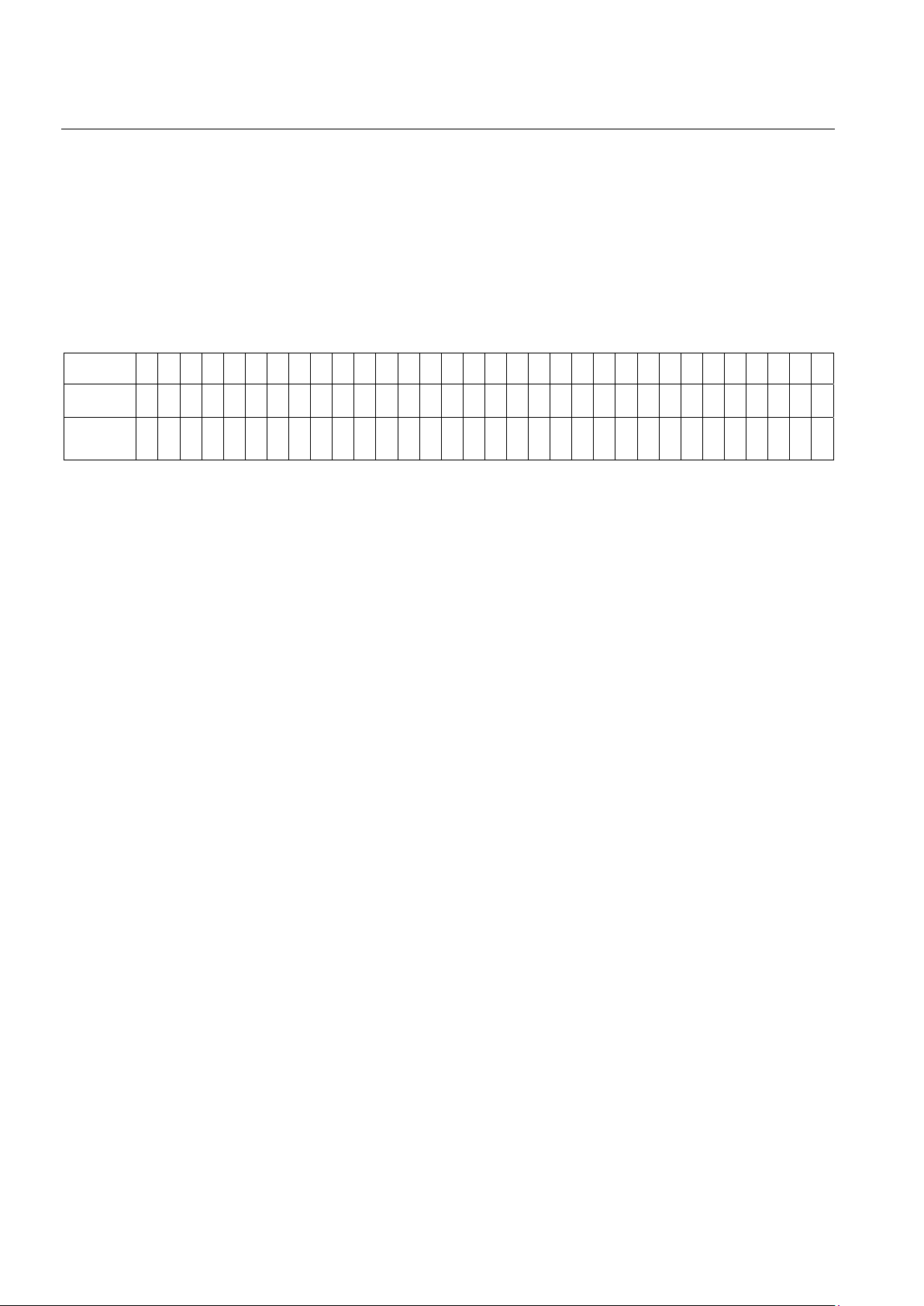
Table 5-1. Time Slot Numbering Schemes
TS
0 1 2 3 4 5 6 7 8 9 10 11 12 13 14 15 16 17 18 19 20 21 22 23 24 25 26 27 28 29 30 31
Channel
1 2 3 4 5 6 7 8 9 10 11 12 13 14 15 16 17 18 19 20 21 22 23 24 25 26 27 28 29 30 31 32
Phone
Channel
1 2 3 4 5 6 7 8 9 10 11 12 13 14 15 16 17 18 19 20 21 22 23 24 25 26 27 28 29 30

DS26518 8-Port T1/E1/J1 Transceiver
17 of 286
6. MAJOR OPERATING MODES
The DS26518 has two major modes of operation: T1 mode and E1 mode. The mode of operation for each LIU is
configured in the
LTRCR register. The mode of operation for each framer is configured in the TMMR register. J1
operation is a special case of T1 operating mode.
DS26518 8-Port T1/E1/J1 Transceiver
18 of 286
7. BLOCK DIAGRAMS
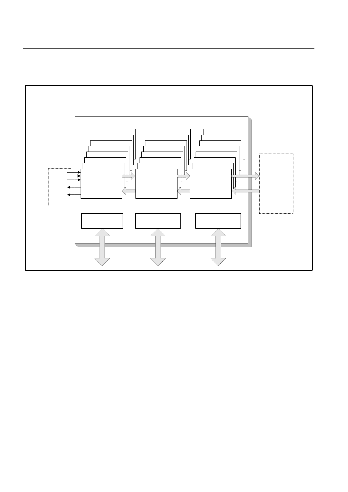
Figure 7-1. Block Diagram
x8
DS26518
FRAMER #8
FRAMER #7
FRAMER #6
...
FRAMER #4
FRAMER #3
FRAMER #2
T1/E1 FRAMER
HDLC
BERT
MICRO PROCESSOR
INTERFACE
JTAG PORT
CLOCK
GENERATION
LIU #8
LIU #7
LIU #6
...
LIU #4
LIU #3
LIU #2
LINE
INTERFACE
UNIT
INTERFACE #8
INTERFACE #7
INTERFACE #6
...
INTERFACE #4
INTERFACE #3
INTERFACE #2
BACKPLANE
INTERFACE
ELASTIC
STORES
RTIP
TRING
RRING
TTIP
CONTROLLER
PORT
TEST
PORT
CLOCK
ADAPTER
RECEIVE
BACKPLANE
SIGNALS
TRANSMIT
BACKPLANE
SIGNALS
HARDWARE
ALARM
INDICATORS
x8
RTIPE
DS26518 8-Port T1/E1/J1 Transceiver
19 of 286
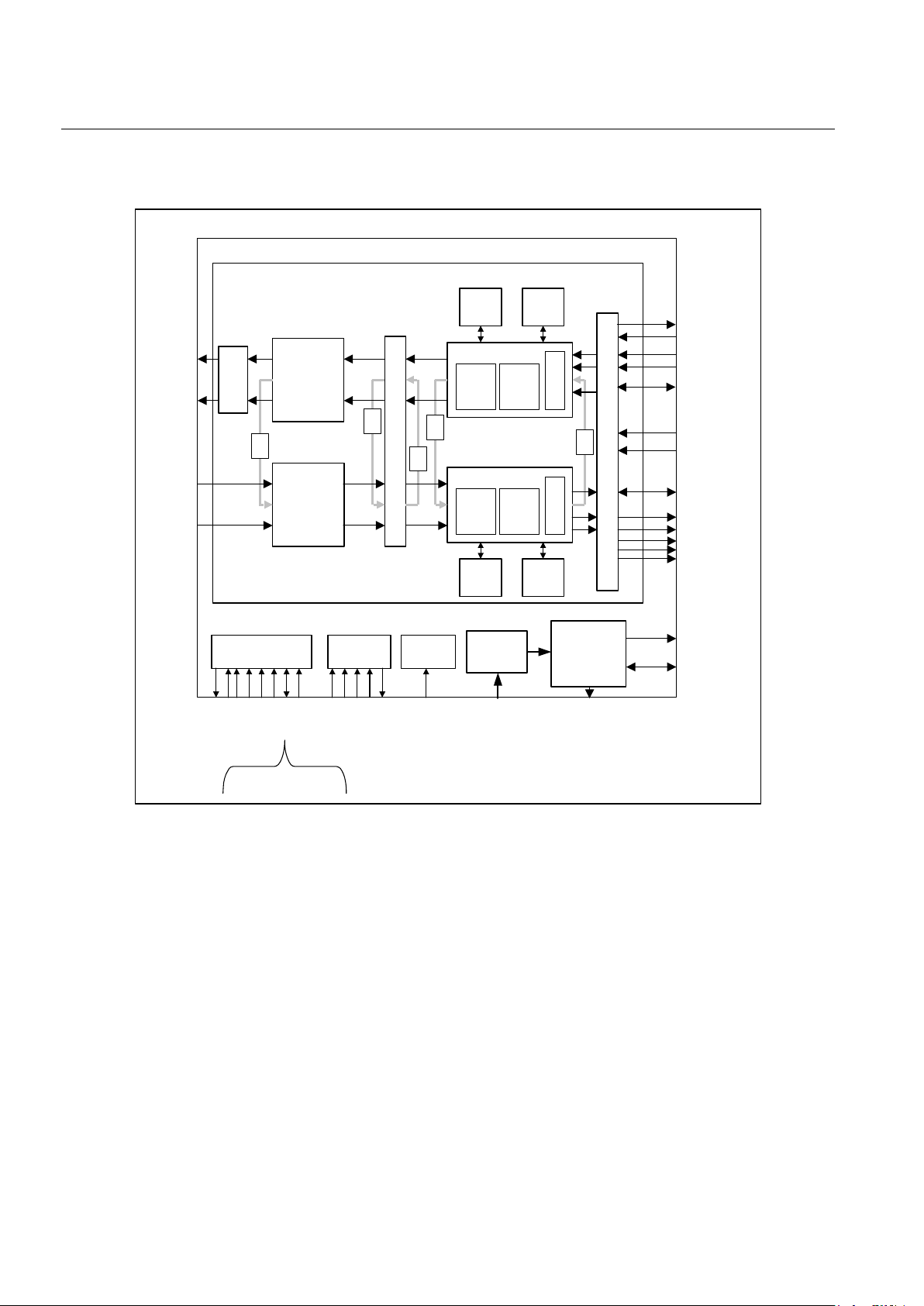
Figure 7-2. Detailed Block Diagram
CLOCK
SYNTHESIZ-
ER
MICROPROCESSOR
INTERFACE
JTAG
PORT
RESET
BLOCK
A[12:0]
D[7:0]
CSB
RDB/DSB
WRB/RWB
BTS
INTB
JTDI
JTMS
JTCLK
JTDO
JTRST
RESETB
MCLK
RCHBLK/CLKn
TCHBLK/CLKn
TCLKn
TSERn
TSYNCn/
TSSYNCIOn
TSYSCLKn
RSYSCLKn
RSYNCn
RSERn
RCLKn
BPCLK1
REFCLKIO
TTIPn
TRINGn
RRINGn
RTIPn
Serial Interface Mode:
SPI
(SCLK, CPOL, CPHA,
SWAP, MOSI, and MISO)
RSIGn
RM/RFSYNCn
TSIGn
PRE-SCALER
PLL
SPI_SEL
CLKO
TRANSMIT
LIU
Waveform
Shaper/Line
Driver
RECEIVE
LIU
Clock/Data
Recovery
JITTER ATTENUATOR
TRANSMIT
ENABLE
Tx
BERT
Rx
BERT
Tx
HDLC
Rx
HDLC
Tx FRAMER:
System IF
B8ZS/
HDB3
Encode
Elastic
Store
Rx FRAMER:
System IF
B8ZS/
HDB3
Decode
Elastic
Store
ALB
LLB
FLB
RLB
PLB
DS26518
TRANSCEIVER 1 OF 8
BACKPLANE INTERFACE
DS26518 8-Port T1/E1/J1 Transceiver
20 of 286
8. PIN DESCRIPTIONS
8.1 Pin Functional Description
Table 8-1. Detailed Pin Descriptions
NAME PIN TYPE FUNCTION
ANALOG TRANSMIT
TTIP1 A1, A2
TTIP2 H1, H2
TTIP3 J1 J2
TTIP4 T1, T2
TTIP5 T15, T16
TTIP6 J15, J16
TTIP7 H15, H16
TTIP8 A15, A16
Analog
Output,
High
Impedance
Transmit Bipolar Tip for Transceiver 1 to 8. These pins are differential line
driver tip outputs. These pins can be high impedance if:
If TXENABLE is low, TTIPn/TRINGn will be high impedance. Note that if
TXENABLE is low, the register settings for control of TTIPn/TRINGn are ignored
and output is high impedance.
The differential outputs of TTIPn and TRINGn can provide internal matched
impedance for E1 75Ω, E1 120Ω, T1 100Ω, or J1 110Ω. The user can turn off
internal termination.
Note: The two pins shown for each transmit bipolar tip (e.g., pins A1 and A2 for
TTIP1) should be tied together.
TRING1 A3, B3
TRING2 G3, H3
TRING3 J3, K3
TRING4 R3, T3
TRING5 R14,T14
TRING6 J14, K14
TRING7 G14, H14
TRING8 A14, B14
Analog
Output,
High
Impedance
Transmit Bipolar Ring for Transceiver 1 to 8. These pins are differential line
driver ring outputs. These pins can be high impedance if:
If TXENABLE is low, TTIPn/TRINGn will be high impedance. Note that if
TXENABLE is low, the register settings for control of TTIPn/TRINGn are ignored
and output is high impedance.
The differential outputs of TTIPn and TRINGn can provide internal matched
impedance for E1 75Ω, E1 120Ω, T1 100Ω, or J1 110Ω. The user can turn off
internal termination.
Note: The two pins shown for each transmit bipolar ring (e.g., pins A3 and B3 for
TRING1) should be tied together.
TXENABLE/
SCAN_EN
L13 Input
Transmit Enable. If this pin is pulled low, all transmitter outputs (TTIPn and
TRINGn) are high impedance. The register settings for tri-state control of
TTIPn/TRINGn are ignored if TXENABLE is low. If TXENABLE is high, the
particular driver can be tri-stated by the register settings.
Scan Enable. When low, device is in normal operation. Scan enable is selected
by the SCANMODE pin. Note: User should not select scan enable—test mode
only.
ANALOG RECEIVE
RTIP1 C1
RTIP2 F1
RTIP3 L1
RTIP4 P1
RTIP5 P16
RTIP6 L16
RTIP7 F16
RTIP8 C16
Analog
Input
Receive Bipolar Tip for Transceiver 1 to 8. The differential inputs of RTIPn
and RRINGn can provide internal matched impedance for E1 75Ω, E1 120Ω, T1
100Ω, or J1 110Ω. The user can turn off internal termination via the LIU Receive
Impedance and Sensitivity Monitor register (
LRISMR).
RRING1 C2
RRING2 F2
RRING3 L2
RRING4 P2
RRING5 P15
RRING6 L15
RRING7 F15
RRING8 C15
Analog
Input
Receive Bipolar Ring for Transceiver 1 to 8. The differential inputs of RTIPn
and RRINGn can provide internal matched impedance for E1 75Ω, E1 120Ω, T1
100Ω, or J1 110Ω. The user has the option of turning off internal termination via
the LIU Receive Impedance and Sensitivity Monitor register (
LRISMR).
RESREF J5 Input
Resistor Reference. This pin is used to calibrate the internal impedance match
resistors of the receive LIUs. This pin should be tied to V
SS
through a 10kΩ ±1%
resistor.
DS26518 8-Port T1/E1/J1 Transceiver
21 of 286
NAME PIN TYPE FUNCTION
TRANSMIT FRAMER
TSER1 F6
TSER2 E7
TSER3 R4
TSER4 N7
TSER5 M10
TSER6 L11
TSER7 F10
TSER8 D12
Input
Transmit NRZ Serial Data 1 to 8. These pins are sampled on the falling edge of
TCLKn when the transmit-side elastic store is disabled. These pins are sampled
on the falling edge of TSYSCLKn when the transmit-side elastic store is enabled.
In IBO mode, data for multiple framers can be used in high-speed multiplexed
scheme. This is described in Section
9.8.2. The table there presents the
combination of framer data for each of the streams.
TSYSCLKn is used as a reference when IBO is invoked. See Table 9-8.
TCLK1 C5
TCLK2 D7
TCLK3 P5
TCLK4 L8
TCLK5 L10
TCLK6 N11
TCLK7 E10
TCLK8 B13
Input
Transmit Clock 1 to 8. A 1.544MHz or a 2.048MHz primary clock. Used to clock
data through the transmit side of the transceiver. TSERn data is sampled on the
falling edge of TCLKn. TCLKn is used to sample TSERn when the elastic store is
not enabled or IBO is not used.
TSYSCLK1 P13 Input
Transmit System Clock 1. 1.544MHz, 2.048MHz, 4.096MHz, 8.192MHz, or
16.384MHz clock. Only used when the transmit-side elastic store function is
enabled. Should be tied low in applications that do not use the transmit-side
elastic store. The clock can be 4.096MHz, 8.912MHz, or 16.384MHz when IBO
mode is used. TSYSCLK1 does not have an internal pulldown resistor. Note: If
the
GTCR1.528MD bit is set, TSYSCLK1 becomes the master TSYSCLK for all
framers.
TSYSCLK2/
AL/RSIGF/FLOS2
F3
TSYSCLK3/
AL/RSIGF/FLOS3
L3
TSYSCLK4/
AL/RSIGF/FLOS4
P3
TSYSCLK5/
AL/RSIGF/FLOS5
P14
TSYSCLK6/
AL/RSIGF/FLOS6
L14
TSYSCLK7/
AL/RSIGF/FLOS7
F14
TSYSCLK8/
AL/RSIGF/FLOS8
C14
Input with
internal
pulldown/
Output
Transmit System Clock 2 to 8. 1.544MHz, 2.048MHz, 4.096MHz, 8.192MHz, or
16.384MHz clock. Only used when the transmit-side elastic store function is
enabled. Should be tied low in applications that do not use the transmit-side
elastic store. The clock can be 4.096MHz, 8.912MHz, or 16.384MHz when IBO
mode is used. TSYSCLK1 does not have an internal pulldown resistor. Note: If
the
GTCR1.528MD bit is set, TSYSCLK1 becomes the master TSYSCLK for all
framers.
Analog Loss/Receive-Signaling Freeze/Framer LOS. Analog LOS reflects the
LOS (loss of signal) detected by the LIU front-end and framer LOS is LOS
detection by the corresponding framer; the same pins can reflect receivesignaling freeze indications. This selection can be made by settings in the Global
Transceiver Clock Control Register 1 (
GTCCR1).
AL/RSIGF/FLOS[8:2] is available only by setting the
GTCR1.528MD bit to 1.
TSYNC1/
TSSYNCIO1
B4
TSYNC2/
TSSYNCIO2
F7
TSYNC3/
TSSYNCIO3
M6
TSYNC4/
TSSYNCIO4
M7
TSYNC5/
TSSYNCIO5
N10
TSYNC6/
TSSYNCIO6
T12
TSYNC7/
TSSYNCIO7
B11
TSYNC8/
TSSYNCIO8
A13
Input/
Output
Transmit Synchronization 1 to 8. A pulse at these pins establishes either frame
or multiframe boundaries for the transmit side. These signals can also be
programmed to output either a frame or multiframe pulse. If these pins are set to
output pulses at frame boundaries, they can also be set to output double-wide
pulses at signaling frames in T1 mode. The operation of these signals is
synchronous with TCLK[8:1].
Transmit System Synchronization In. These pins are selected when the
transmit-side elastic store is enabled. A pulse at these pins establishes either
frame or multiframe boundaries for the transmit side. Should be tied low in
applications that do not use the transmit-side elastic store. The operation of this
signal is synchronous with TSYSCLK[8:1].
Transmit System Synchronization Out. If configured as an output and the
transmit elastic store is enabled, an 8kHz pulse synchronous to the BPCLK1 will
be generated. This pulse in combination with BPCLK1 can be used as an IBO
master. TSSYNCIOn can be used as a source to RSYNCn and TSSYNCIOn of
another DS26518 or RSYNC and TSSYNC of other Dallas Semiconductor parts.
Note: TSSYNCIO[8:1] are not used when
GTCR1.528MD is set. When
GTCR1.528MD is set, the TSSYNCIO pin (N13) is used.

DS26518 8-Port T1/E1/J1 Transceiver
22 of 286
NAME PIN TYPE FUNCTION
TSSYNCIO N13
Input/
Output
Note: In default operation, this pin is not used. When
GTCR1.528MD is set,
this pin is active. If pin is not used, tie low through a resistor.
Transmit System Synchronization In. This pin is selected when the transmitside elastic store is enabled. A pulse at this pin establishes either frame or
multiframe boundaries for the transmit side. Note that if the elastic store is
enabled, frame or multiframe boundary will be established for all transmitters.
Should be tied low in applications that do not use the transmit-side elastic store.
The operation of this signal is synchronous with TSYSCLKn.
Transmit System Synchronization Out. If configured as an output and the
transmit-side elastic store is enabled, an 8kHz pulse synchronous to BPCLK1 will
be generated. This pulse in combination with BPCLK1 can be used as an IBO
master. TSSYNCIO can be used as a source to RSYNCn and TSSYNCIO of
another DS26518 or RSYNC and TSSYNC of other Dallas Semiconductor parts.
TSIG1 D5
TSIG2 A6
TSIG3 T4
TSIG4 R6
TSIG5 T10
TSIG6 R12
TSIG7 A11
TSIG8 C13
Input
Transmit Signaling 1 to 8. When enabled, this input samples signaling bits for
insertion into outgoing PCM data stream. Sampled on the falling edge of TCLKn
when the transmit-side elastic store is disabled. Sampled on the falling edge of
TSYSCLKn when the transmit-side elastic store is enabled. In IBO mode, the
TSIGn streams can run up to 16.384MHz. See
Table 9-9.
TCHBLK1/
TCHCLK1
A5
TCHBLK2/
TCHCLK2
C7
TCHBLK3/
TCHCLK3
L7
TCHBLK4/
TCHCLK4
P7
TCHBLK5/
TCHCLK5
P9
TCHBLK6/
TCHCLK6
P11
TCHBLK7/
TCHCLK7
D10
TCHBLK8/
TCHCLK8
E11
Output
Transmit Channel Block/Transmit Channel Block Clock. A dual function pin.
TCHBLK[1:8]. TCHBLKn is a user-programmable output that can be forced high
or low during any of the channels. It is synchronous with TCLKn when the
transmit-side elastic store is disabled. It is synchronous with TSYSCLKn when
the transmit-side elastic store is enabled. It is useful for blocking clocks to a serial
UART or LAPD controller in applications where not all channels are used such as
Fractional T1, Fractional E1, 384kbps (H0), 768kbps, or ISDN-PRI. Also useful
for locating individual channels in drop-and-insert applications, for external per-
channel loopback, and for per-channel conditioning.
TCHCLK[1:8]. TCHCLKn is a 192kHz (T1) or 256kHz (E1) clock that pulses high
during the LSB of each channel. It can also be programmed to output a gated
transmit bit clock controlled by TCHBLKn. It is synchronous with TCLKn when the
transmit-side elastic store is disabled. It is synchronous with TSYSCLKn when
the transmit-side elastic store is enabled. Useful for parallel-to-serial conversion
of channel data.
DS26518 8-Port T1/E1/J1 Transceiver
23 of 286
NAME PIN TYPE FUNCTION
RECEIVE FRAMER
RSER1 E5
RSER2 D6
RSER3 N4
RSER4 N6
RSER5 M11
RSER6 M12
RSER7 B12
RSER8 F11
Output
Received Serial Data 1 to 8. Received NRZ serial data. Updated on rising edges
of RCLKn when the receive-side elastic store is disabled. Updated on the rising
edges of RSYSCLKn when the receive-side elastic store is enabled.
When IBO mode is used, the RSERn pins can output data for multiple framers.
The RSERn data is synchronous to RSYSCLKn. See Section
9.8.2 and Table
9-6
.
RCLK1 F4
RCLK2 G4
RCLK3 L4
RCLK4 M4
RCLK5 K13
RCLK6 J13
RCLK7 F13
RCLK8 E13
Output
Receive Clock 1 to 8. A 1.544MHz (T1) or 2.048MHz (E1) clock that is used to
clock data through the receive-side framer. This clock is recovered from the
signal at RTIPn and RRINGn. RSERn data is output on the rising edge of
RCLKn. RCLKn is used to output RSERn when the elastic store is not enabled or
IBO is not used. When the elastic store is enabled or IBO is used, the RSERn is
clocked by RSYSCLKn.
RSYSCLK1 L12 Input
Receive System Clock 1. 1.544MHz, 2.048MHz, 4.096MHz, 8.192MHz, or
16.384MHz receive backplane clock. Only used when the receive-side elastic
store function is enabled. Should be tied low in applications that do not use the
receive-side elastic store. Multiple of 2.048MHz is expected when the IBO mode
is used. Note: If the
GTCR1.528MD bit is set, RSYSCLK1 becomes the master
RSYSCLK for all framers.
RSYSCLK2/
RLF/LTC2
E3
RSYSCLK3/
RLF/LTC3
M3
RSYSCLK4/
RLF/LTC4
N3
RSYSCLK5/
RLF/LTC5
N14
RSYSCLK6/
RLF/LTC6
M14
RSYSCLK7/
RLF/LTC7
E14
RSYSCLK8/
RLF/LTC8
D14
Input with
internal
pulldown/
Output
Receive System Clock 2 to 8. 1.544MHz, 2.048MHz, 4.096MHz, 8.192MHz, or
16.384MHz receive backplane clock. Only used when the receive-side elastic
store function is enabled. Should be tied low in applications that do not use the
receive-side elastic store. Multiple of 2.048MHz is expected when the IBO Mode
is used.
Receive Loss of Frame/Loss of Transmit Clock. This pin can also be
programmed to either toggle high when the synchronizer is searching for the
frame and multiframe or to toggle high if the TCLKn pin has not been toggled for
approximately three clock periods.
RLF/LTC[8:2] are available when
GTCR1.528MD = 1.
Note: If the GTCR1.528MD bit is set, RSYSCLK1 becomes the master
RSYSCLK for all framers.
RSYNC1 A4
RSYNC2 B6
RSYNC2 N5
RSYNC2 T6
RSYNC5 R10
RSYNC6 P12
RSYNC7 C11
RSYNC8 D13
Input/
Output
Receive Synchronization 1 to 8. If the receive-side elastic store is enabled, this
signal is used to input a frame or multiframe boundary pulse. If set to output
frame boundaries, RSYNCn can be programmed to output double-wide pulses on
signaling frames in T1 mode. In E1 mode, RSYNCn out can be used to indicate
CAS and CRC-4 multiframe. The DS26518 can accept an H.100-compatible
synchronization signal. The default direction of this pin at power-up is input, as
determined by the RSIO control bit in the
RIOCR.2 register.
DS26518 8-Port T1/E1/J1 Transceiver
24 of 286
NAME PIN TYPE FUNCTION
RMSYNC1/
RFSYNC1
C4
RMSYNC2/
RFSYNC2
C6
RMSYNC3/
RFSYNC3
P4
RMSYNC4/
RFSYNC4
P6
RMSYNC5/
RFSYNC5
P10
RMSYNC6/
RFSYNC6
N12
RMSYNC7/
RFSYNC7
D11
RMSYNC8/
RFSYNC8
E12
Output
Receive Multiframe/Frame Synchronization 1 to 8. A dual function pin to
indicate frame or multiframe synchronization. RFSYNCn is an extracted 8kHz
pulse, one RCLKn wide that identifies frame boundaries. RMSYNCn is an
extracted pulse, one RCLKn wide (elastic store disabled) or one RSYSCLKn wide
(elastic store enabled), that identifies multiframe boundaries. When the receive
elastic store is enabled, the RMSYNCn signal indicates the multiframe sync on
the system (backplane) side of the elastic store. In E1 mode, this pin can indicate
either the CRC-4 or CAS multiframe as determined by the RSMS2 control bit in
the Receive I/O Configuration register (
RIOCR.1).
RSIG1 D4
RSIG2 E6
RSIG3 M5
RSIG4 R5
RSIG5 R11
RSIG6 R13
RSIG7 A12
RSIG8 F12
Output
Receive Signaling 1 to 8. Outputs signaling bits in a PCM format. Updated on
rising edges of RCLKn when the receive-side elastic store is disabled. Updated
on the rising edges of RSYSCLKn when the receive-side elastic store is enabled.
See
Table 9-7.
RCHBLK1/
RCHCLK1
E4
RCHBLK2/
RCHCLK2
B5
RCHBLK3/
RCHCLK3
L6
RCHBLK4/
RCHCLK4
T5
RCHBLK5/
RCHCLK5
T11
RCHBLK6/
RCHCLK6
T13
RCHBLK7/
RCHCLK7
C12
RCHBLK8/
RCHCLK8
G13
Output
Receive Channel Block/Receive Channel Block Clock. This pin can be
configured to output either RCHBLK or RCHCLK.
RCHBLK[1:8]. RCHBLKn is a user-programmable output that can be forced high
or low during any of the 24 T1 or 32 E1 channels. It is synchronous with RCLKn
when the receive-side elastic store is disabled. It is synchronous with RSYSCLKn
when the receive-side elastic store is enabled. This pin is useful for blocking
clocks to a serial UART or LAPD controller in applications where not all channels
are used such as fractional service, 384kbps service, 768kbps, or ISDN-PRI.
Also useful for locating individual channels in drop-and-insert applications, for
external per-channel loopback, and for per-channel conditioning.
RCHCLK[1:8]. RCHCLKn is a 192kHz (T1) or 256kHz (E1) clock that pulses high
during the LSB of each channel. It is synchronous with RCLKn when the receive-
side elastic store is disabled. It is synchronous with RSYSCLKn when the
receive-side elastic store is enabled. It is useful for parallel-to-serial conversion of
channel data.
BPCLK1 E8 Output
Backplane Clock 1. Programmable clock output that can be set to 2.048MHz,
4.096MHz, 8.192MHz, or 16.384MHz. The reference for this clock can be
RCLK[8:1], a 1.544MHz or 2.048MHz clock frequency derived from MCLK, or an
external reference clock (REFCLKIO). This allows system clocks to be
referenced from external sources, the T1J1E1 recovered clocks, or the MCLK
oscillator.
CLKO/
RLF/LTC1
D3 Output
Clock Out. Clock output pin that can be programmed to output numerous
frequencies referenced to MCLK. Frequencies available: 1.544MHz, 2.048MHz,
4.096MHz, 8.192MHz, 12.288MHz, 16.384MHz, 256kHz, and 64kHz.
GTCCR3.CLKOSEL[2:0] selects the frequency.
Receive Loss of Frame/Loss of Transmit Clock. This pin can also be
programmed to either toggle high when the synchronizer is searching for the
frame and multiframe, or to toggle high if the TCLKn pin has not been toggled for
approximately three clock periods.
RLF/LTC1 is available on the DS26518 when
GTCR1.528MD = 1.
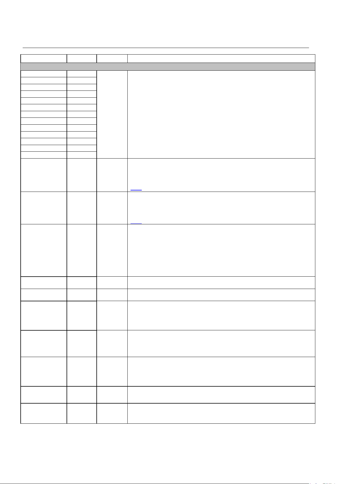
DS26518 8-Port T1/E1/J1 Transceiver
25 of 286
NAME PIN TYPE FUNCTION
MICROPROCESSOR INTERFACE
A12 C8
A11 A8
A10 B8
A9 F8
A8 B9
A7 A9
A6 C9
A5 D9
A4 E9
A3 F9
A2 B10
A1 A10
A0 C10
Input
Address [12:0]. This bus selects a specific register in the DS26518 during
read/write access. A12 is the MSB and A0 is the LSB.
D[7]/SPI_CPOL T9
Input/
Output
Data [7]/SPI Interface Clock Polarity
D[7]: Bit 7 of the 16-bit or 8-bit data bus used to input data during register writes
and data outputs during register reads. Not driven when CSB = 1.
SPI_CPOL: This signal selects the clock polarity when SPI_SEL = 1. See Section
9.1.2 for detailed timing and functionality information. Default setting is low.
D[6]/SPI_CPHA N9
Input/
Output
Data [6]/SPI Interface Clock Phase
D[6]: Bit 6 of the 16-bit or 8-bit data bus used to input data during register writes
and data outputs during register reads. Not driven when CSB = 1.
SPI_CPHA: This signal selects the clock phase when SPI_SEL = 1. See Section
9.1.2 for detailed timing and functionality information. Default setting is low.
D[5]/SPI_SWAP M9
Input/
Output
Data [5]/SPI Bit Order Swap
D[5]: Bit 5 of the 16-bit or 8-bit data bus used to input data during register writes
and data outputs during register reads. Not driven when CSB = 1.
SPI_SWAP: This signal is active when SPI_SEL = 1. The address and data bit
order is swapped when SPI_SWAP is high. The R/W and B bit positions are
never changed in the control word.
0 = LSB is transmitted and received first.
1 = MSB is transmitted and received first.
D[4] R8
Input/
Output
Data [4]. Bit 4 of the 8-bit data bus used to input data during register writes and
data outputs during register reads. Not driven when CSB = 1.
D[3] T8
Input/
Output
Data [3]. Bit 3 of the 8-bit data bus used to input data during register writes and
data outputs during register reads. Not driven when CSB = 1.
D[2]/SPI_SCLK P8
Input/
Output
Data [2]/SPI Serial Interface Clock
D[2]: Bit 2 of the 8-bit data bus used to input data during register writes and data
outputs during register reads. Not driven when CSB = 1.
SPI_SCLK: SPI Serial Clock Input when SPI_SEL = 1.
D[1]/SPI_MOSI L9
Input/
Ouput
Data [1]/SPI Serial Interface Data Master Out-Slave In
D[1]: Bit 1 of the 8-bit data bus used to input data during register writes, and data
outputs during register reads. Not driven when CSB = 1.
SPI_MOSI: SPI Serial Data Input (Master Out-Slave In) when SPI_SEL = 1.
D[0]/SPI_MISO N8
Input/
Output
Data [0]/SPI Serial Interface Data Master In-Slave Out
D[0]: Bit 0 of the 8-bit data bus used to input data during register writes and data
outputs during register reads. Not driven when CSB = 1.
SPI_MISO: SPI Serial Data Output (Master In-Slave Out) when SPI_SEL = 1.
CSB
T7 Input
Chip-Select Bar. This active-low signal is used to qualify register read/write
accesses. The RDB/DSB and WRB signals are qualified with CSB.
RDB/
DSB
M8 Input
Read-Data Bar/Data-Strobe Bar. This active-low signal along with CSB qualifies
read access to one of the DS26518 registers. The DS26518 drives the data bus
with the contents of the addressed register while RDB and CSB are low.
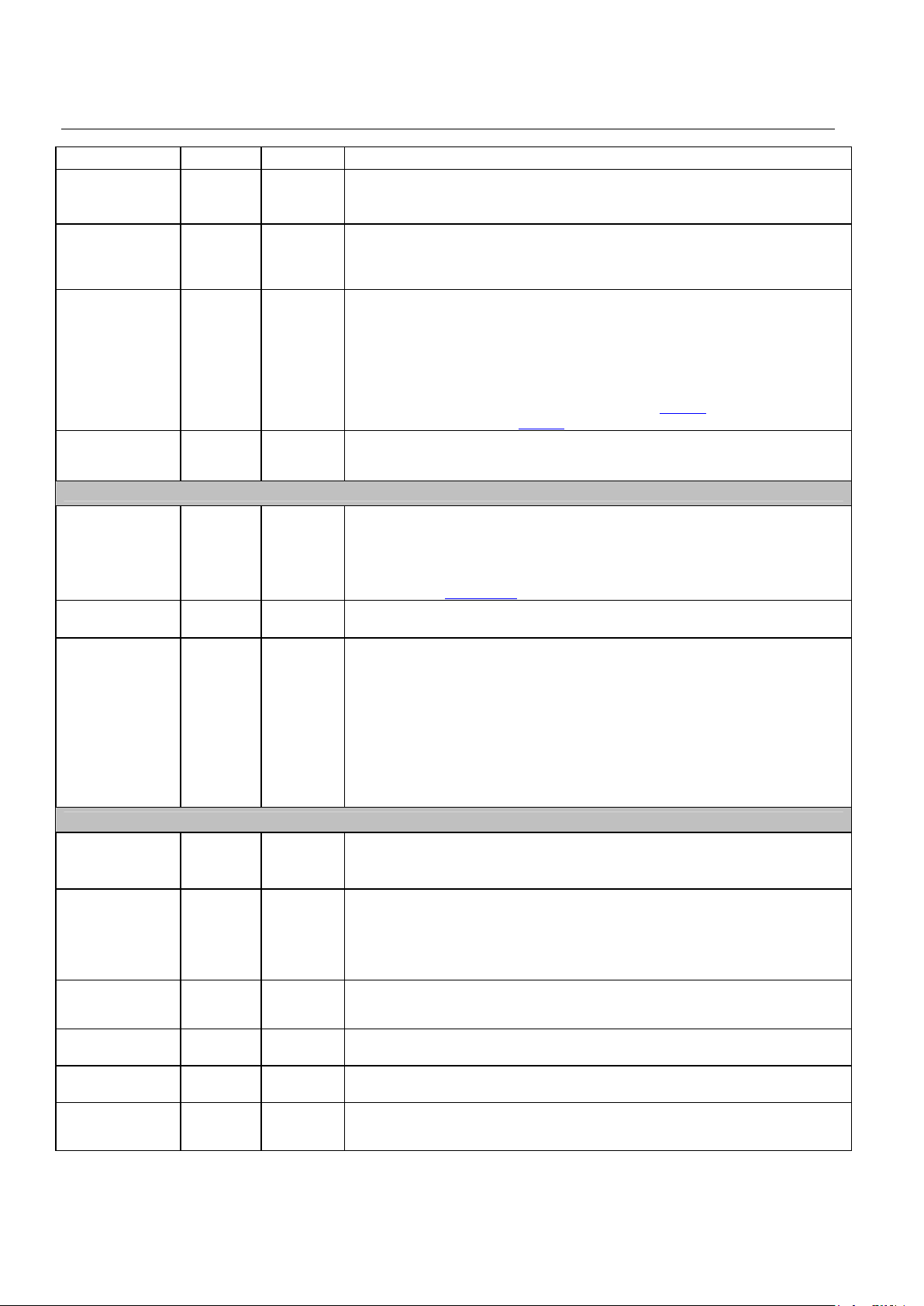
DS26518 8-Port T1/E1/J1 Transceiver
26 of 286
NAME PIN TYPE FUNCTION
WRB/
RWB
R7 Input
Write-Read Bar/Read-Write Bar. This active-low signal along with CSB qualifies
write access to one of the DS26518 registers. Data at D[7:0] is written into the
addressed register at the rising edge of WRB while CSB is low.
INTB
R9
Output,
Tri-
Stateable
Interrupt Bar. This active-low output is asserted when an unmasked interrupt
event is detected. INTB will be deasserted (and tri-stated) when all interrupts
have been acknowledged and serviced. Extensive mask bits are provided at the
global level, framer, LIU, and BERT level.
SPI_SEL/
AL/RSIGF/FLOS1
C3
Input with
internal
pulldown/
Output
SPI Serial Bus Mode Select/Analog Loss/Receive Signaling Freeze/Framer
LOS
SPI_SEL: 0 = Parallel Bus Mode, 1 = SPI Serial Bus Mode
AL/RSIGF/FLOS1: Analog LOS reflects the loss of signal detected by the LIU
front-end; framer LOS is LOS detection by the corresponding framer. The same
pins can reflect receive-signaling freeze indications. This selection can be made
by settings in Global Transceiver Control Register (
GTCR1). AL/RSIGF/FLOS1
are available by setting the
GTCR1.528MD bit to 1.
BTS M13 Input
Bus Type Select. Set high to select Motorola bus timing, low to select Intel bus
timing. This pin controls the function of the RDB/DSB and WRB pins. Note: If SPI
mode is selected by the SPI_SEL pin, this pin must be tied low.
SYSTEM INTERFACE
MCLK B7 Input
Master Clock. This is an independent free-running clock whose input can be a
multiple of 2.048MHz ±50ppm or 1.544MHz ±50ppm. The clock selection is
available by bits MPS0 and MPS1 and FREQSEL. Multiple of 2.048MHz can be
internally adapted to 1.544MHz. Multiple of 1.544MHz can be adapted to
2.048MHz. Note that TCLKn must be 2.048MHz for E1 and 1.544MHz for T1/J1
operation. See
Table 10-12.
RESETB
J12 Input
Reset Bar. Active-low reset. This input forces the complete DS26518 reset. This
includes reset of the registers, framers, and LIUs.
REFCLKIO A7
Input/
Output
Reference Clock Input/Output
Input: A 2.048MHz or 1.544MHz clock input. This clock can be used to generate
the backplane clock. This allows for the users to synchronize the system
backplane with the reference clock. The other options for the backplane clock
reference are LIU-received clocks or MCLK.
Output: This signal can also be used to output a 1.544MHz or 2.048MHz
reference clock. This allows for multiple DS26518s to share the same reference
for generation of the backplane clock. Hence, in a system consisting of multiple
DS26518s, one can be a master and others a slave using the same reference
clock.
TEST
DIGIOEN D8
Input,
Pullup
Digital Enable. When this pin and JTRST are pulled low, all digital I/O pins are
placed in a high-impedance state. If this pin is high the digital I/O pins operate
normally. This pin must be connected to V
DD
for normal operation.
JTRST
L5
Input,
Pullup
JTAG Reset. JTRST is used to asynchronously reset the test access port
controller. After power-up, JTRST must be toggled from low to high. This action
sets the device into the JTAG DEVICE ID mode. Pulling JTRST low restores
normal device operation. JTRST is pulled high internally via a 10kΩ resistor
operation. If boundary scan is not used, this pin should be held low.
JTMS K4
Input,
Pullup
JTAG Mode Select. This pin is sampled on the rising edge of JTCLK and is used
to place the test access port into the various defined IEEE 1149.1 states. This pin
has a 10kΩ pullup resistor.
JTCLK F5 Input
JTAG Clock. This signal is used to shift data into JTDI on the rising edge and out
of JTDO on the falling edge.
JTDI H4
Input,
Pullup
JTAG Data In. Test instructions and data are clocked into this pin on the rising
edge of JTCLK. This pin has a 10kΩ pullup resistor.
JTDO J4
Output,
High
Impedance
JTAG Data Out. Test instructions and data are clocked out of this pin on the
falling edge of JTCLK. If not used, this pin should be left unconnected.
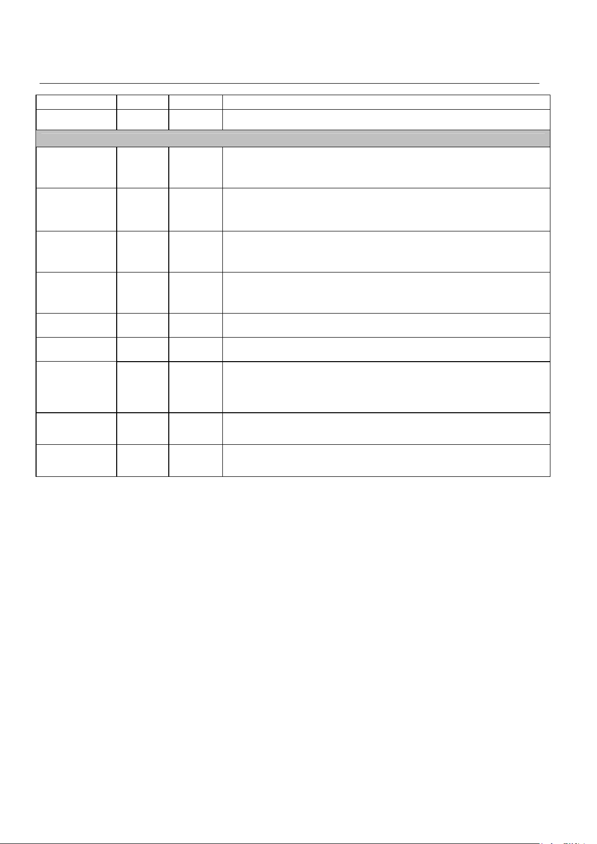
DS26518 8-Port T1/E1/J1 Transceiver
27 of 286
NAME PIN TYPE FUNCTION
SCANMODE H13 Input
Scan Mode. When low, normal operational clocks are used to clock the flip flops.
User should tie low.
POWER SUPPLIES
ATVDD
B1, B16,
G1, G16,
K1, K16,
R1, R16
—
3.3V ±5% Analog Transmit Power Supply. These V
DD
inputs are used for the
transmit LIU sections of the DS26518.
ATVSS
B2, B15,
G2, G15,
K2, K15,
R2, R15
—
Analog Transmit VSS. These pins are used for transmit analog VSS.
ARVDD
D1, D16,
E1, E16,
M1, M16,
N1, N16
—
3.3V ±5% Analog Receive Power Supply. These V
DD
inputs are used for the
receive LIU sections of the DS26518.
ARVSS
D2, D15,
E2, E15,
M2, M15,
N2, N15
—
Analog Receive V
SS
. These pins are used for analog VSS for the receivers.
ACVDD H7 —
1.8V ±5% Analog Clock Conversion V
DD
. This VDD input is used for the clock
conversion unit (CLAD) of the DS26518.
ACVSS J7 —
Analog Clock V
SS
. This pin is used for clock converter analog VSS.
DVDD33
G5, G6,
G11, G12,
H5, H6,
H8, H9,
H10, H11
—
3.3V ±5% Power Supply for I/Os
DVDD18 G7–G10 —
1.8V ±5% Power Supply for Internal V
DD
DVSS
H12, J6,
J8–J11,
K5–K12
—
Digital Ground

DS26518 8-Port T1/E1/J1 Transceiver
28 of 286
9. FUNCTIONAL DESCRIPTION
9.1 Processor Interface
Microprocessor control of the DS26518 is accomplished through the 28 hardware pins of the microprocessor port.
The 8-bit parallel data bus can be configured for Intel or Motorola modes of operation with the bus type select
(BTS) pin. When the BTS pin is a logic 0, bus timing is in Intel mode, as shown in
Figure 13-2 and Figure 13-3.
When the BTS pin is a logic 1, bus timing is in Motorola mode, as shown in
Figure 13-4 and Figure 13-5. The
address space is mapped through the use of 13 address lines, A[12:0]. Multiplexed mode is not supported on the
processor interface.
The chip-select bar (CSB) pin must be brought to a logic-low level to gain read and write access to the
microprocessor port. With Intel timing selected, the read-data bar (RDB) and write-read bar (WRB) pins are used to
indicate read and write operations and latch data through the interface. With Motorola timing selected, the readwrite bar (RWB) pin is used to indicate read and write operations while the data-strobe bar (DSB) pin is used to
latch data through the interface.
The interrupt output pin (INTB) is an open-drain output that asserts a logic-low level upon a number of software
maskable interrupt conditions. This pin is normally connected to the microprocessor interrupt input.
9.1.1 SPI Serial Port Mode
The external processor bus can be configured to operate in SPI serial bus mode. See Section 9.1.2 for detailed
timing diagrams.
When SPI_SEL = 1, SPI bus mode is implemented using four signals: clock (SPI_SCLK), master out-slave in data
(SPI_MOSI), master in-slave out data (SPI_MISO), and chip select (CSB). Clock polarity and phase can be set by
the D[7]/SPI_CPOL and D[6]/SPI_CPHA pins.
The order of the address and data bits in the serial stream is selectable using the D[5]/SPI_SWAP pin. The R/W bit
is always first and B bit is always last in the initial control word and are not effected by the D[5]/SPI_SWAP pin
setting.
SPI mode is not recommended for HDLC operations because of the bandwidth constraints of SPI.
9.1.2 SPI Functional Timing Diagrams
Note: The transmit and receive order of the address and data bits are selected by the D[5]/SPI_SWAP pin. The
R/W (read/write) MSB bit and B (burst) LSB bit position is not affected by the D[5]/SPI_SWAP pin setting.
9.1.2.1 SPI Transmission Format and CPHA Polarity
When SPI_CPHA = 0, CSB may be deasserted between accesses. An access is defined as one or two control
bytes followed by a data byte. CSB cannot be deasserted between the control bytes, or between the last control
byte and the data byte. When SPI_CPHA = 0, CSB may also remain asserted between accesses. If it remains
asserted and the BURST bit is set, no additional control bytes are expected after the first control byte(s) and data
are transferred. If the BURST bit is set, the address will be incremented for each additional byte of data transferred
until CSB is deasserted. If CSB remains asserted and the BURST bit is not set, a control byte(s) is expected
following the data byte, and the address for the next access will be received from that. Anytime CSB is deasserted,
the BURST access is terminated.
When SPI_CPHA = 1, CSB may remain asserted for more than one access without being toggled high and then
low again between accesses. If the BURST bit is set, the address should increment and no additional control bytes
are expected. If the BURST bit is not set, each data byte will be followed by the control byte(s) for the next access.
Additionally, CSB may also be deasserted between accesses when SPI_CPHA = 1. In the case, any BURST
access is terminated and the next byte received when CSB is reasserted will be a control byte.
The following diagrams describe the functionality of the SPI port for the four combinations of SPI_CPOL and
SPI_CPHA. They indicate the clock edge that samples the data and the level of the clock during no-transfer events
(high or low). Since the SPI port of the DS26518 acts as a slave device, the master device provides the clock. The
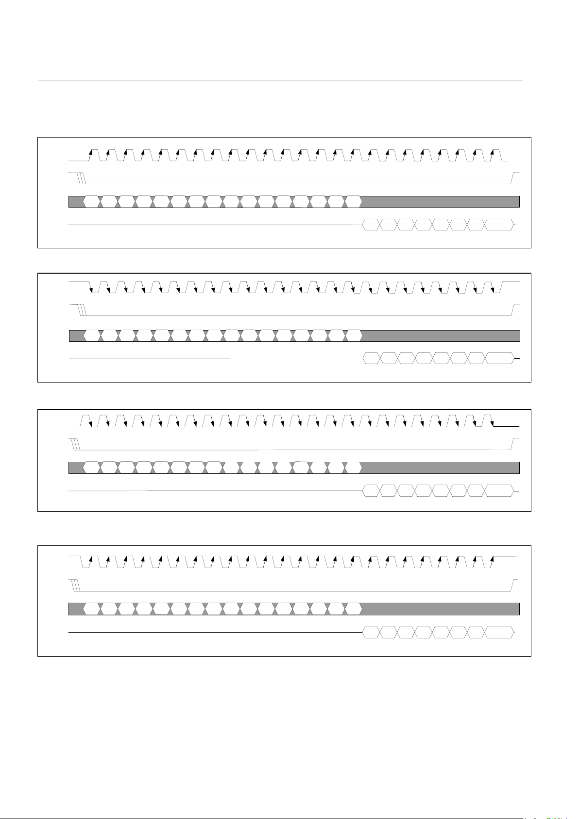
DS26518 8-Port T1/E1/J1 Transceiver
29 of 286
user must configure the SPI_CPOL and SPI_CPHA pins to describe which type of clock that the master device is
providing.
Figure 9-1. SPI Serial Port Access for Read Mode, SPI_CPOL = 0, SPI_CPHA = 0
1
A7
A13 A12 A11 A10 A9 A8
D7 D6 D5 D4 D3 D2 D1 D0
LSBMSB
LSB
MSB
SPI_SCLK
C
SB
SPI_MOSI
SPI_MISO
B
A6 A5 A4 A3 A2 A1
LSBMSB
A0
Figure 9-2. SPI Serial Port Access for Read Mode, SPI_CPOL = 1, SPI_CPHA = 0
SPI_SCLK
1
A7
A13 A12 A11 A10 A9 A8
D7 D6 D5 D4 D3 D2 D1 D0
LSBMSB
LSB
MSB
SPI_MOSI
SPI_MISO
B
A6 A5 A4 A3 A2 A1
LSBMSB
A0
C
SB
Figure 9-3. SPI Serial Port Access for Read Mode, SPI_CPOL = 0, SPI_CPHA = 1
SPI_SCLK
CSB
1
A
7
A
13
A
12
A
11
A
10
A
9
A
8
D7 D6 D5 D4 D3 D2 D1 D0
LSBMSB
LSB
MSB
SPI_MOSI
SPI_MISO
B
A6A5A4A3A2A
1
LSBMSB
A
0
Figure 9-4. SPI Serial Port Access for Read Mode, SPI_CPOL = 1, SPI_CPHA = 1
SPI_SLCK
CSB
1
A
7
A
13
A
12
A
11
A
10
A
9
A
8
D7 D6 D5 D4 D3 D2 D1 D0
LSBMSB
LSB
MSB
SPI_MOSI
SPI_MISO
B
A6A5A4A3A2A
1
LSBMSB
A
0
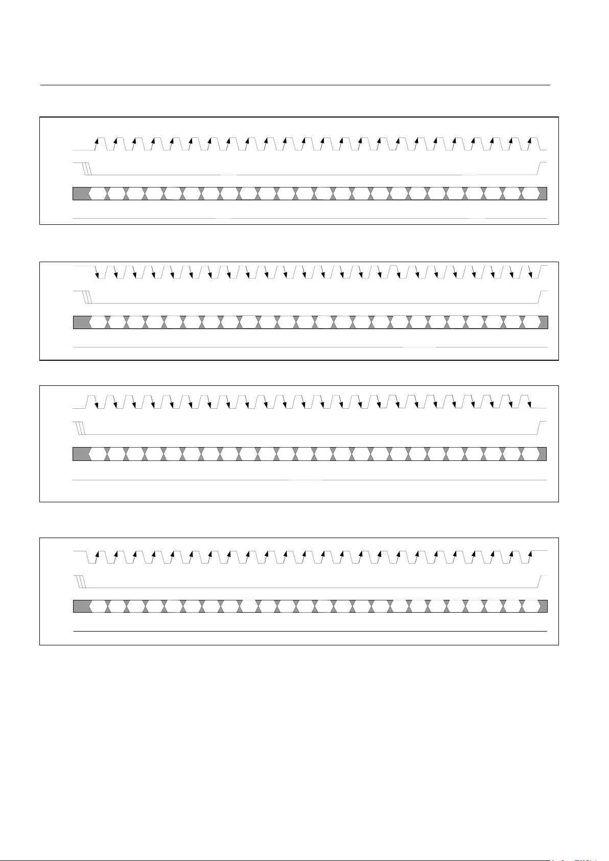
DS26518 8-Port T1/E1/J1 Transceiver
30 of 286
Figure 9-5. SPI Serial Port Access for Write Mode, SPI_CPOL = 0, SPI_CPHA = 0
0
A
13
LSB
MSB
SPI_SCLK
CSB
SPI_MOSI
SPI_MISO
D7 D6 D5 D4 D3 D2 D1 D0
LSBMSB
A4A3A2A1A
0
LSBMSB
A
12
A
11
A
10
A
9
A
8
A
7
A6A
5
B
Figure 9-6. SPI Serial Port Access for Write Mode, SPI_CPOL = 1, SPI_CPHA = 0
SPI_SCLK
CSB
0
A
13
LSB
MSB
SPI_MOSI
SPI_MISO
D7 D6 D5 D4 D3 D2 D1 D0
LSBMSB
A4A3A2A1A
0
LSBMSB
A
12
A
11
A
10
A
9
A
8
A
7
A6A
5
B
Figure 9-7. SPI Serial Port Access for Write Mode, SPI_CPOL = 0, SPI_CPHA = 1
SPI_SCL
K
CSB
0
A
13
LSB
MSB
SPI_MOSI
SPI_MISO
D7 D6 D5 D4 D3 D2 D1 D0
LSBMSB
A4A3A2A1A
0
LSBMSB
A
12
A
11
A
10
A
9
A
8
A
7
A6A
5
B
Figure 9-8. SPI Serial Port Access for Write Mode, SPI_CPOL = 1, SPI_CPHA = 1
SPI_SCLK
CSB
0
A
13
LSB
MSB
SPI_MOSI
SPI_MISO
D7 D6 D5 D4 D3 D2 D1 D0
LSBMSB
A4A3A2A1A
0
LSBMSB
A
12
A
11
A
10
A
9
A
8
A
7
A6A
5
B
 Loading...