Maxim Integrated Producs DS1841 Datasheet
DS1841
Temperature-Controlled, NV, I2C,
Logarithmic Resistor
Rev 0; 11/07
________________________________________________________________
Maxim Integrated Products
1
For pricing, delivery, and ordering information, please contact Maxim Direct at 1-888-629-4642,
or visit Maxim’s website at www.maxim-ic.com.
General Description
The DS1841 is a 7-bit, logarithmic, nonvolatile (NV) digital resistor that features an on-chip temperature sensor
and associated analog-to-digital converter (ADC). The
integrated temperature sensor indexes a 72-byte NV
lookup table (LUT) encompassing a temperature range
from -40°C to +100°C. The LUT output can drive the
resistor directly or be added to an NV initial-value register (IVR) to drive the resistor. This flexible LUT-based
architecture allows the DS1841 to provide a temperature-compensated resistor output with arbitrary slope.
Programming is accomplished by an I2C-compatible
interface, which can operate at speeds of up to 400kHz.
Applications
Optical Transceivers
Linear and Nonlinear Compensation
Instrumentation and Industrial Controls
Mechanical Potentiometer Replacement
Features
♦ 22kΩ to 3.7kΩ Adjustable Logarithmic Resistor
with a 3.6kΩ Fixed Resistor
♦ 128 Wiper Tap Points
♦ On-Chip Temperature Sensor and ADC
♦ 72-Byte Lookup Table (LUT)
♦ I
2
C-Compatible Serial Interface
♦ Address Pins Allow Up to Four DS1841s to Share
the Same I
2
C Bus
♦ Digital Supply of 2.7V to 5.5V
♦ -40°C to +100°C Operating Range
♦ 3mm x 3mm, 10-Pin TDFN Package
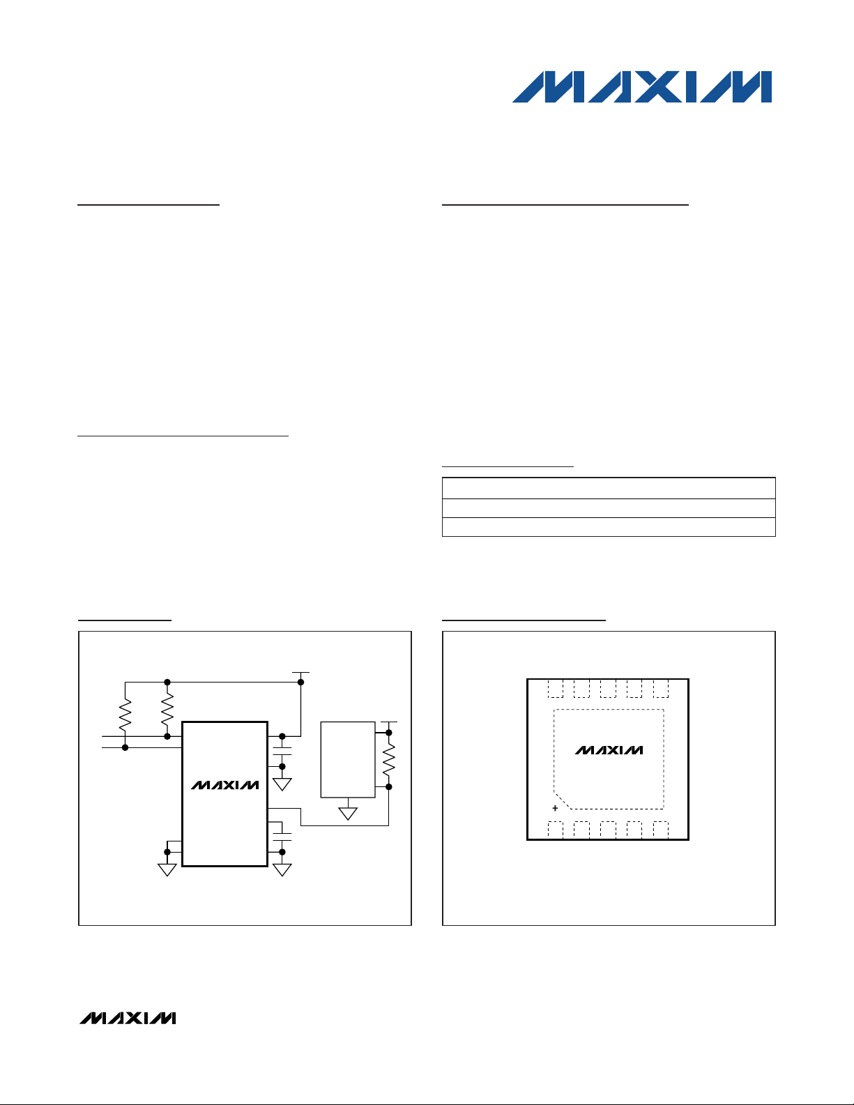
134
10 8 7
SCL RH RW
SDA
*EP
*EXPOSED PAD
V
CC
A1
2
9
N.C.
GND
5
6
RGND
A0
TDFN
3.0mm × 3.0mm × 0.8mm
TOP VIEW
DS1841
Pin Configuration
Ordering Information
0.1μF
3.3V
APD BIAS CONTROL APPLICATION
V
CC
V
OUT
FB
SDA
SCL
A1
A0
GND
100pF
RW
RGND
RH
V
APD
4.7kΩ
4.7kΩ
DC-DC
CONVERTER
DS1841
Typical Operating Circuit
+
Denotes a lead-free package.
T&R = Tape and reel.
Registers and Modes are capitalized for clarity.
PART TEMP RANGE PIN-PACKAGE
DS1841T+ -40°C to +100°C 10 TDFN
DS1841T+T&R -40°C to +100°C 10 TDFN
DS1841
Temperature-Controlled, NV, I2C,
Logarithmic Resistor
2 _______________________________________________________________________________________
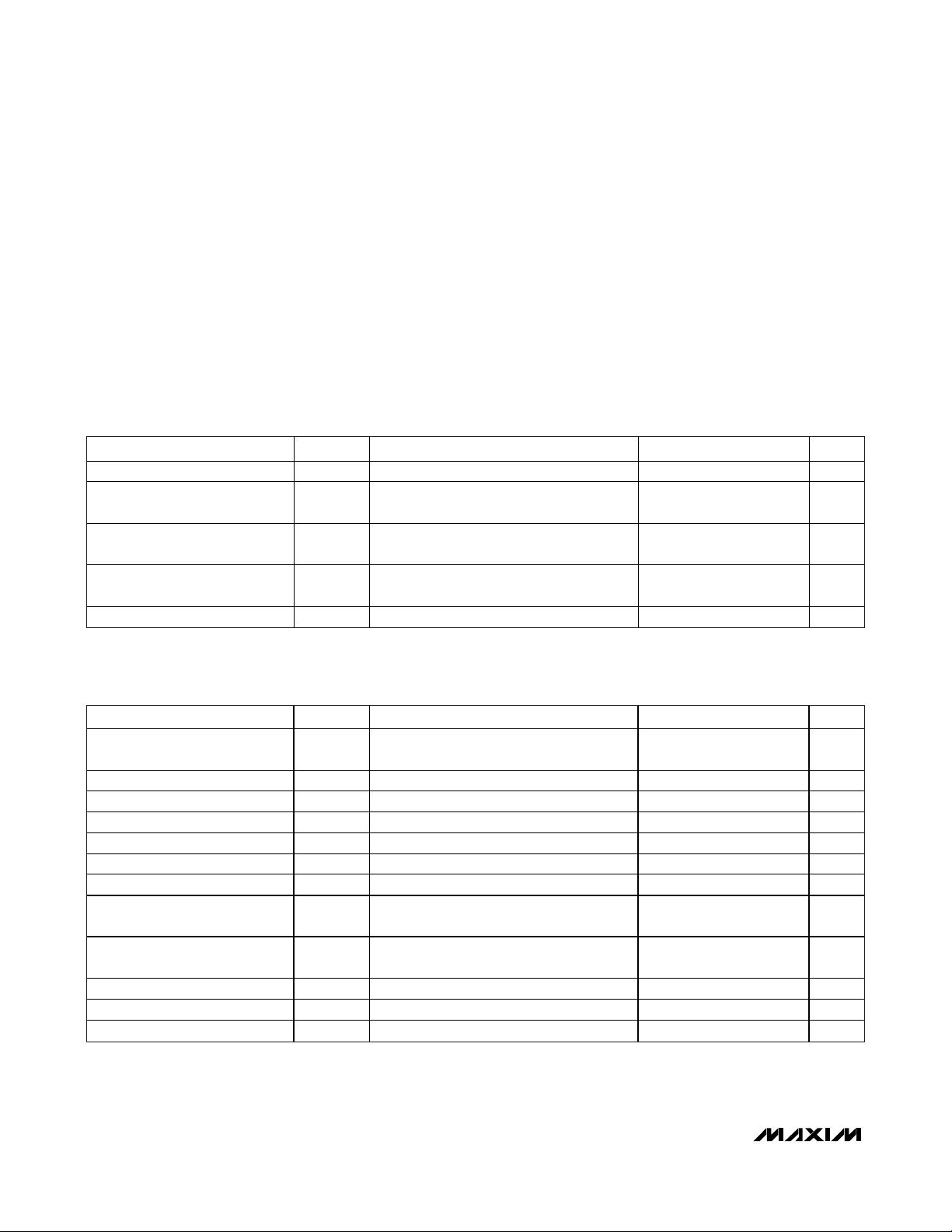
RECOMMENDED OPERATING CONDITIONS
(TA= -40°C to +100°C)
Stresses beyond those listed under “Absolute Maximum Ratings” may cause permanent damage to the device. These are stress ratings only, and functional
operation of the device at these or any other conditions beyond those indicated in the operational sections of the specifications is not implied. Exposure to
absolute maximum rating conditions for extended periods may affect device reliability.
Voltage Range on SDA, SCL, and
V
CC
Relative to GND .........................................-0.5V to +6.0V
Voltage Range on RH, RW, A0, and
A1 Relative to GND ................................-0.5V to (V
CC
+ 0.5V)
Operating Temperature Range .........................-40°C to +100°C
Programming Temperature Range .........................0°C to +70°C
Storage Temperature Range .............................-55°C to +125°C
Soldering Temperature .....................See IPC/JEDEC J-STD-020
RW Current............................................................................3mA
DC ELECTRICAL CHARACTERISTICS
(VCC= +2.7V to +5.5V, TA= -40°C to +100°C, unless otherwise noted.)
ABSOLUTE MAXIMUM RATINGS
PARAMETER SYMBOL CONDITIONS MIN TYP MAX UNITS
Supply Voltage V
Input Logic 1
(SCL, SDA, A0, A1)
Input Logic 0
(SCL, SDA, A0, A1)
Resistor Inputs (RW, RH) V
Wiper Current I
WIPER
CC
V
V
RES
(Note 1) +2.7 +5.5 V
IH
IL
2mA
0.7 x
V
CC
-0.3
-0.3
V
CC
+ 0.3
0.3 x
V
CC
V
CC
+ 0.5
V
V
V
Input Leakage
(SDA, SCL, A0, A1)
VCC Supply C urrent I
Low-Leve l Output Voltage (SDA) V
I/O Capacitance C
Power-On Recall Voltage V
Power-Up Recall Delay tD (Note 4) 5 ms
Series Resistance RS 3.6 k
Minimum Resistance
(GND to RW)
End-to-End Resistance
(GND to RW)
R
TOTAL
Temp Coefficient TCV WR set to 40h ±250 ppm/°C
RH, RW Capacitance C
PARAMETER SYMBOL CONDITIONS MIN TYP MAX UNITS
I
CC2
OL
I/O
POR
R
MIN
R
TOTAL
Tolerance TA= +25°C -20 +20 %
POT
-1 +1 μA
L
(Note 2) 350 μA
3mA sink current 0 0.4 V
5 10 pF
(Note 3) 1.6 2.6 V
(Note 5) 370
22 k
10 pF
DS1841
Temperature-Controlled, NV, I2C,
Logarithmic Resistor
_______________________________________________________________________________________ 3
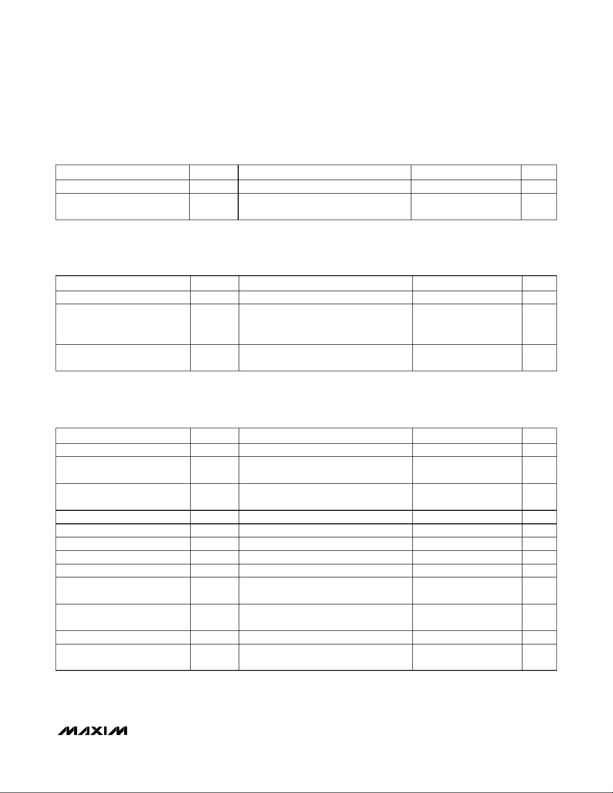
TEMPERATURE SENSOR CHARACTERISTICS
(VCC= +2.7V to +5.5V, TA= -40°C to +100°C, unless otherwise noted.)
ANALOG VOLTAGE MONITORING CHARACTERISTICS
(VCC= +2.7V to +5.5V, TA= -40°C to +100°C, unless otherwise noted.)
I2C AC ELECTRICAL CHARACTERISTICS (See Figure 3)
(VCC= +2.7V to +5.5V, TA= -40°C to +100°C, timing referenced to V
IL(MAX)
and V
IH(MIN)
.)
Temperature Error ±5 °C
Update Rate (Temperature and
Supply Conversion Time)
PARAMETER SYMBOL CONDITIONS MIN TYP MAX UNITS
t
FRAME
16 ms
Supply Resolution LSB Full-scale voltage of 6.5536V 25.6 mV
Input/Supply Accuracy ACC At factory setting 0.25 1.0
Update Rate (Temperature and
Supply Conversion Time)
PARAMETER SYMBOL CONDITIONS MIN TYP MAX UNITS
16 ms
t
FRAME
PARAMETER SYMBOL CONDITIONS MIN TYP MAX UNITS
SCL Clock Frequenc y f
Bus Free Time Between STOP
and START Conditions
Hold Time (Repeated) START
Conditions
Low Period of SCL t
High Period of SCL t
Data Hold Time t
Data Setup Time t
START Setup Time t
SDA a nd SCL Ri se Time t
SDA and SCL Fall Time t
STOP Setup Time t
SDA a nd SCL Capacit i ve
Loading
t
HD: STA
HD:DAT
SU:DAT
SU:STA
SU:STO
SCL
t
BUF
LOW
HIGH
C
(Note 6) 0 400 kH z
1.3 μs
0.6 μs
1.3 μs
0.6 μs
0 0.9 μs
100 ns
0.6 μs
(Note 7)
R
(Note 7)
F
0.6 μs
(Note 7) 400 pF
B
20 +
0.1C
20 +
0.1C
300 ns
B
300 ns
B
% FS
(Full
Scale)
DS1841
Temperature-Controlled, NV, I2C,
Logarithmic Resistor
4 _______________________________________________________________________________________
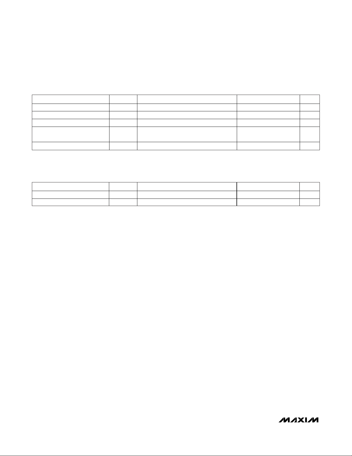
Note 1: All voltages are referenced to ground. Currents entering the IC are specified positive and currents exiting the IC are
negative.
Note 2:I
CC
is specified with the following conditions: SCL and SDA = VCC, RW and RH floating with Update Mode bit = 1.
Note 3: This is the minimum V
CC
voltage that causes NV memory to be recalled.
Note 4: This is the time from V
CC
> V
POR
until initial memory recall is complete.
Note 5: Guaranteed by design.
Note 6: I
2
C interface timing shown is for Fast-Mode (400kHz) operation. This device is also backward-compatible with I2C-
Standard Mode timing.
Note 7: C
B
—total capacitance of one bus line in picofarads.
Note 8: EEPROM write time begins after a STOP condition occurs.
Note 9: Guaranteed by characterization.
I2C AC ELECTRICAL CHARACTERISTICS (See Figure 3) (continued)
(VCC= +2.7V to +5.5V, TA= -40°C to +100°C, timing referenced to V
IL(MAX)
and V
IH(MIN)
.)
NONVOLATILE MEMORY CHARACTERISTICS
(VCC= +2.7V to +5.5V)
PARAMETER SYMBOL CONDITIONS MIN TYP MAX UNITS
EEPROM Write Time t
A0, A1 Setup Time t
A0, A1 Hold Time t
Input Capacitance on
A0, A1, SDA, or SCL
Startup Time t
SU:A
HD:A
C
ST
(Note 8) 10 20 ms
W
Before START 0.6 μs
After STOP 0.6 μs
5 10 pF
I
2 ms
EEPROM Write Cycles TA = +85°C 50,000 Writes
EEPROM Write Cycles TA = +25°C (Note 9) 200,000 Writes
PARAMETER SYMBOL CONDITIONS MIN TYP MAX UNITS
DS1841
Temperature-Controlled, NV, I2C,
Logarithmic Resistor
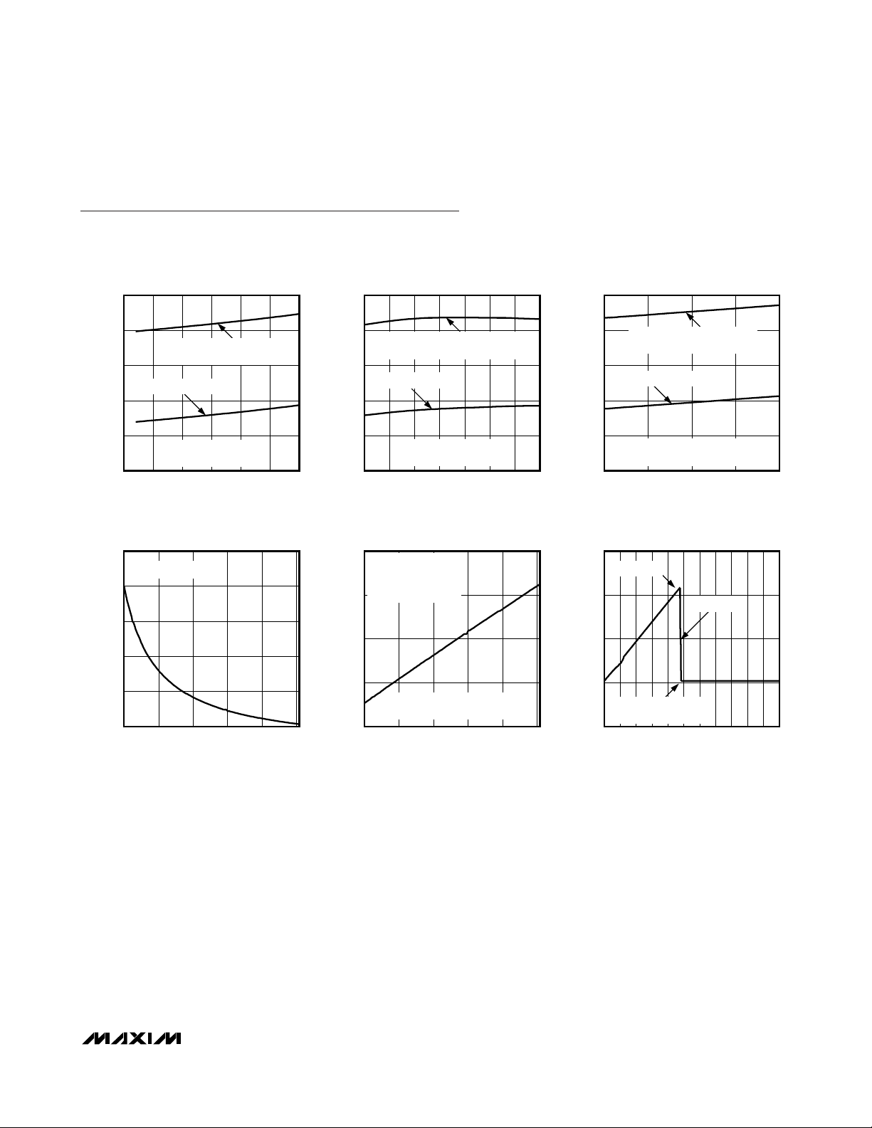
SUPPLY CURRENT
vs. SUPPLY VOLTAGE
DS1841 toc01
SUPPLY VOLTAGE (V)
SUPPLY CURRENT (mA)
5.04.54.03.53.0
50
100
150
200
250
0
2.5 5.5
SDA = SCL = VCC
RH, RH, RW ARE FLOATING
SDA = SCL = V
CC
RGND, RH, RW ARE FLOATING
UPDATE MODE BIT = 0UPDATE MODE BIT = 0
LUT MODE AND LUT ADDER MODE
UPDATE MODE BIT = 1
LUT MODE AND LUT ADDER MODE
UPDATE MODE BIT = 1
SUPPLY CURRENT
vs. TEMPERATURE
DS1841 toc02
TEMPERATURE (°C)
SUPPLY CURRENT (mA)
806040200-20
50
100
150
200
250
0
-40 100
SDA = SCL = VCC
RH, RH, RW ARE FLOATING
SDA = SCL = VCC = 5V
RGND, RH, RW ARE FLOATING
UPDATE MODE BIT = 0UPDATE MODE BIT = 0
LUT MODE AND LUT ADDER MODE
UPDATE MODE BIT = 1
LUT MODE AND LUT ADDER MODE
UPDATE MODE BIT = 1
SUPPLY CURRENT
vs. SCL FREQUENCY
DS1841 toc03
SCL FREQUENCY (kHz)
SUPPLY CURRENT (mA)
300200100
50
100
150
200
250
0
0 400
SDA = SCL = VCC
RH, RH, RW ARE FLOATING
SDA = VCC = 5V
RGND, RH, RW ARE FLOATING
UPDATE MODE BIT = 0UPDATE MODE BIT = 0
LUT MODE AND LUT ADDER MODE
UPDATE MODE BIT = 1
LUT MODE AND LUT ADDER MODE
UPDATE MODE BIT = 1
WIPER RESISTANCE (RW)
vs. SETTING
DS1841 toc04
SETTING (DEC)
WIPER RESISTANCE (kΩ)
125100755025
5
10
15
20
25
0
0
SDA = SCL = VCC = 5VSDA = SCL = VCC = 5V
WIPER CURRENT
vs. WIPER SETTING
DS1841 toc05
WIPE SETTING (DEC)
WIPER CURRENT (mA)
100755025
0.4
0.8
1.2
1.6
0
0 125
RGND = 0V
RW OPEN
FORCE 1.25V ON RH AND
MEASURE CURRENT
RGND = 0V
RW OPEN
FORCE 1.25V ON RH AND
MEASURE CURRENT
VCC = 5V
SDA AND SCL REFERENCED TO 5V
VCC = 5V
SDA AND SCL REFERENCED TO 5V
RW TO RGND RESISTANCE
vs. SUPPLY VOLTAGE
DS1841 toc06
SUPPLY VOLTAGE (V)
RESISTANCE AT RW (kΩ)
5.04.54.03.53.02.52.01.51.00.5
10
20
30
40
0
0 5.5
POR OCCURSPOR OCCURS
IVR IS LOADED
IVR IS LOADED
CONVERSIONS COMPLETE
LUT VALUE LOADED TO WR
CONVERSIONS COMPLETE
LUT VALUE LOADED TO WR
Typical Operating Characteristics
(VCC= +2.7V to +5.5V, TA= +25°C, unless otherwise noted.)
_______________________________________________________________________________________
5
 Loading...