Maxim Integrated Producs DS1372U+, DS1372 Datasheet

General Description
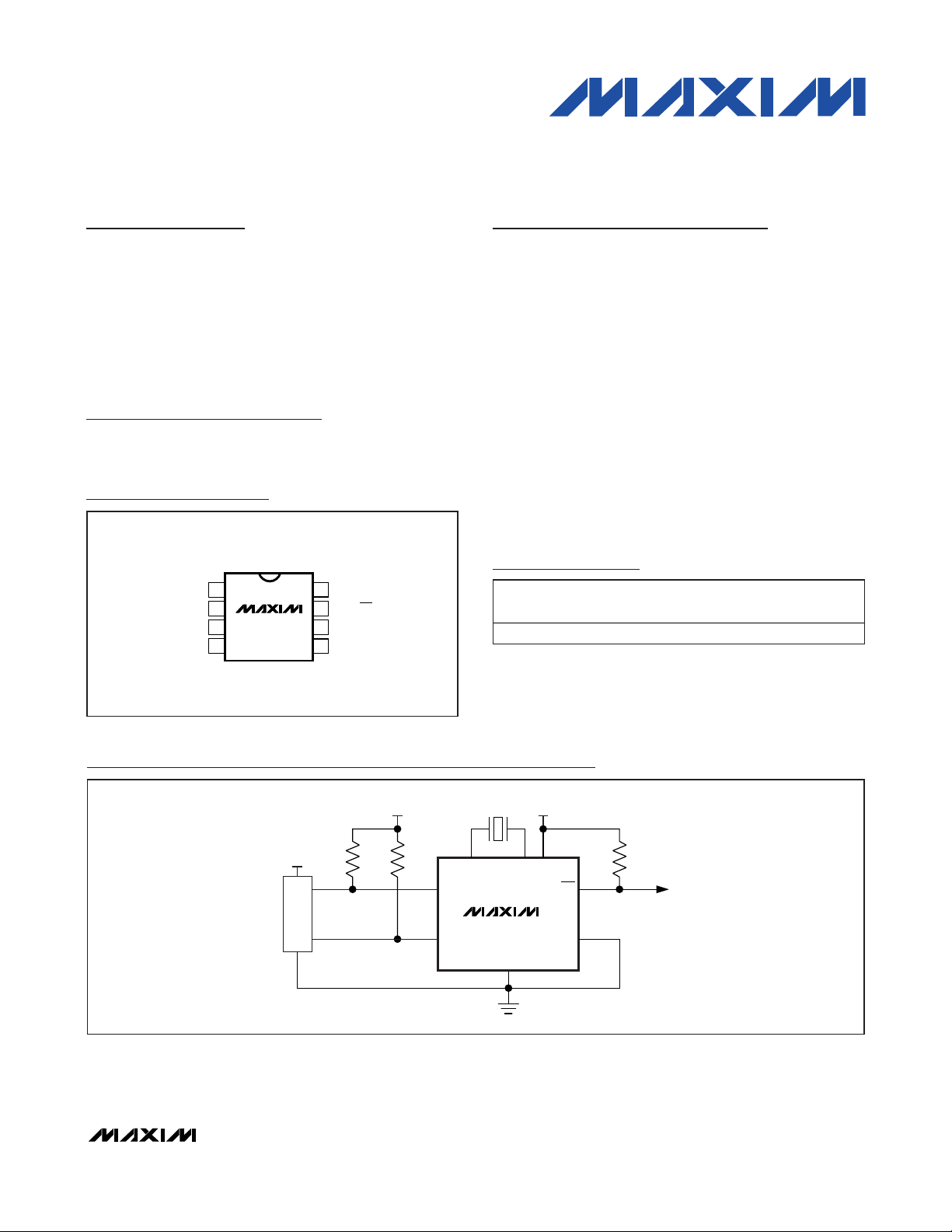
The DS1372 is a 32-bit binary up counter and 24-bit
down counter with a unique 64-bit ID. The counters, ID,
configuration, and status registers are accessed using
an I2C serial interface. The DS1372 includes a
SQW/INT open-drain output that can output either a
square wave at one of four predefined frequencies, or it
can output an active-low signal when the 24-bit down
counter reaches 0.
Applications
Portable Audio and Video Players
Features
♦ Compliant with Microsoft Windows Media®DRM
10 for Portable Devices
♦ 32-Bit Binary Counter
♦ Programmable Alarm
♦ 64-Bit Factory-Programmed ID
♦ Interrupt Output
♦ I
2
C Serial Interface
♦ Two Selectable I
2
C Addresses
♦ 2.4V to 5.5V Operating Voltage Range
♦ 1.3V to 5.5V Timekeeping Operating Range
♦ -40°C to +85°C Operating Temperature Range
♦ 8-Pin µSOP
DS1372
________________________________________________________________
Maxim Integrated Products
1
μ
Pin Configuration
Ordering Information
SCL
SDA
SQW/INT
GND
R
PU
RPU = tR / C
B
R
PU
CPU
V
CC
V
CC
X1 X2 V
CC
CRYSTAL
V
CC
DS1372
AD0
Typical Operating Circuit
Rev 0; 7/07
For pricing, delivery, and ordering information, please contact Maxim Direct at 1-888-629-4642,
or visit Maxim’s website at www.maxim-ic.com.
+
Denotes a lead-free package. This symbol also appears on the
top mark.
Windows Media is a registered trademark of Microsoft Corp.
I2C, 32-Bit, Binary Counter Clock with 64-Bit ID
TOP VIEW
AD0
+
X1
1
X2
2
DS1372
3
4
SOP
8
7
6
5
V
CC
SQW/INT
SCL
SDAGND
PART TEMP RANGE PIN-PACKAGE
DS1372U+ -40°C to +85°C 8 μSOP 1372
TOP
MARK

DS1372
2 _______________________________________________________________________________________
ABSOLUTE MAXIMUM RATINGS
RECOMMENDED DC ELECTRICAL CHARACTERISTICS
(VCC= 2.4V to 5.5V, TA= -40°C to +85°C, unless otherwise noted.) (Note 1)
Stresses beyond those listed under “Absolute Maximum Ratings” may cause permanent damage to the device. These are stress ratings only, and functional
operation of the device at these or any other conditions beyond those indicated in the operational sections of the specifications is not implied. Exposure to
absolute maximum rating conditions for extended periods may affect device reliability.
Voltage Range on Any Pin Relative to Ground…..-0.3V to +6.0V
Continuous Power Dissipation (T
A
= +70°C)
(derate 4.5mW/°C above +70°C) ……………………. ....360mW
Operating Temperature Range
(noncondensing)……. .......................................-40°C to +85°C
Storage Temperature Range…………………….-55°C to +125°C
Soldering Temperature………….......See IPC/JEDEC J-STD-020
specification.
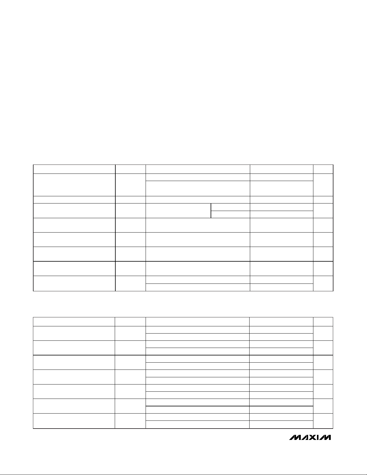
ELECTRICAL CHARACTERISTICS
(VCC= 2.4V to 5.5V, TA= -40°C to +85°C, unless otherwise noted.) (Note 1)
I2C, 32-Bit, Binary Counter Clock with 64-Bit ID
Supply Voltage V
Active Supply Current I
Standby Current
(Oscillator Enabled)
Data Retention
(Oscil lator Disabled)
Input Logic 1
AD0, SCL, SDA
Input Logic 0
AD0, SCL, SDA
Input Leakage
AD0, SCL, SDA, SQW/INT
Output Logic 0 I
PARAMETER SYMBOL CONDITIONS MIN TYP MAX UNITS
Operating voltage range (Notes 2 and 3) 2.4 5.5
Timekeeping operating range
(Notes 2 and 4)
(Note 3) 35 90 μA
EOSC = 0
(Notes 4 and 5)
EOSC = 1 (Note 4) 25 100 nA
(Note 2)
IH
(Note 2) -0.3
IL
SDA, SQW/INT high impedance -1 +1 μA
VOL = 0.4V (VCC > 2.4V), SDA, SQW/INT 3
VOL = 0.2VCC (1.3V < VCC < 2.4V), SQW/INT 0.250
CCA
I
CCS
I
DDR
V
V
I
OL
CC
LI
1.3 5.5
SQW = 32kHz 600 1300
SQW = 0 400 800
0.7 x
V
CC
VCC +
0.3
0.3 x
V
CC
V
nA
V
V
mA
SCL Clock Frequency (Note 6) f
Bus-Free Time Between a STOP
and START Condition
Hold Time (Repeated) START
Condition (Note 7)
Low Period of SCL Clock t
High Period of SCL Clock t
Setup Time for Repeated START
Condition
Data Hold Time (Notes 8 and 9) t
PARAMETER SYMBOL CONDITIONS MIN TYP MAX UNITS
SCL
t
BUF
t
HD:STA
LOW
HIGH
t
SU:STA
HD:DAT
Fast mode 100 400
Standard mode 0.04 100.00
Fast mode 1.3
Standard mode 4.7
Fast mode 0.6
Standard mode 4.0
Fast mode 1.3
Standard mode 4.7
Fast mode 0.6
Standard mode 4.0
Fast mode 0.6
Standard mode 4.7
Fast mode 0 0.9
Standard mode 0
kHz
μs
μs
μs
μs
μs
μs

DS1372
_______________________________________________________________________________________ 3
Note 1: Limits at -40°C are guaranteed by design and not production tested.
Note 2: All voltages are referenced to ground.
Note 3: SCL clocking at maximum frequency = 400kHz.
Note 4: Specified with I
2
C bus inactive, SCL = SDA = VCC.
Note 5: Measured with a 32.768kHz crystal attached to the X1 and X2 pins.
Note 6: The I
2
C minimum operating frequency is imposed by the requirement of timeout period.
Note 7: The first clock pulse is generated after this period.
Note 8: A device must internally provide a hold time of at least 300ns for the SDA signal (referred to as the V
IHMIN
of the SCL sig-
nal) to bridge the undefined region of the falling edge of SCL.
Note 9: The maximum t
HD:DAT
must only be met if the device does not stretch the low period (t
LOW
) of the SCL signal.
Note 10: A fast-mode device can be used in a standard-mode system, but the requirement t
SU:DAT
≥ 250ns must then be met.
This is automatically the case if the device does not stretch the low period of the SCL signal. If such a device does stretch
the low period of the SCL signal, it must output the next data bit to the SDA line t
R(MAX)
+ t
SU:DAT
= 1000 + 250 = 1250ns
before the SCL line is released.
Note 11: C
B
= Total capacitance of one bus line in pF.
Note 12: The parameter t
OSF
is the period of time the oscillator must be stopped for the OSF flag to be set over the voltage range of
2.4V ≤ V
CC
≤ V
CC(MAX)
.
Note 13: The DS1372 can detect any single SCL clock held low longer than T
_TIMEOUT
(MIN). The I2C interface is in reset state and
can receive a new START condition when SCL is held low for at least T
_TIMEOUT
(MAX). Once the part detects this condi-
tion the SDA output is released. The oscillator must be running for this function to work.
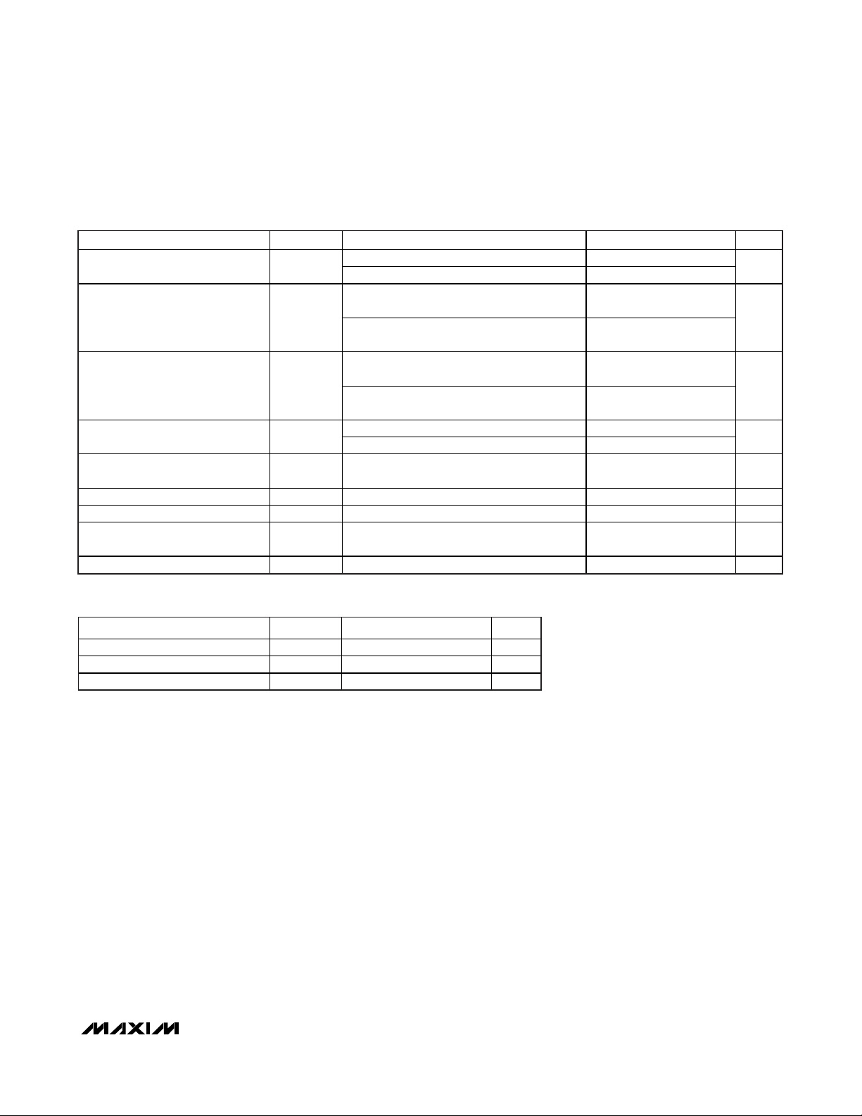
ELECTRICAL CHARACTERISTICS (continued)
(VCC= 2.4V to 5.5V, TA= -40°C to +85°C, unless otherwise noted.) (Note 1)
CRYSTAL SPECIFICATIONS
PARAMETER SYMBOL MIN TYP MAX UNITS
Nominal Frequency f
O
32.768 kHz
Capacitive Load C
L
12.5 pF
Equivalent Series Resistance ESR 50 k
I2C, 32-Bit, Binary Counter Clock with 64-Bit ID
Data Setup Time (Note 10) t
Rise Time of SDA and SCL
Signals (Note 11)
Fall Time of SDA and SCL Signals
(Note 11)
Setup Time for STOP Condition t
Capacitive Load for Each Bus
Line (Note 11)
I/O Capacitance C
SCL Spike Suppresion TSP 30 ns
Oscillator Stop Flag (OSF) Delay
(Note 12)
Timeout Interval (Note 13) T
PARAMETER SYMBOL CONDITIONS MIN TYP MAX UNITS
SU:DAT
t
R
t
SU:STO
C
I/O
t
OSF
_TIMEOUT
Fast mode 100
Standard mode 250
Fast mode
Standard mode
Fast mode
F
Standard mode
20 +
0.1C
20 +
0.1C
20 +
0.1C
20 +
0.1C
300
B
1000
B
300
B
300
B
Fast mode 0.6
Standard mode 4.0
400 pF
B
10 pF
100 ms
25 35 ms
ns
ns
ns
μs

DS1372
4 _______________________________________________________________________________________
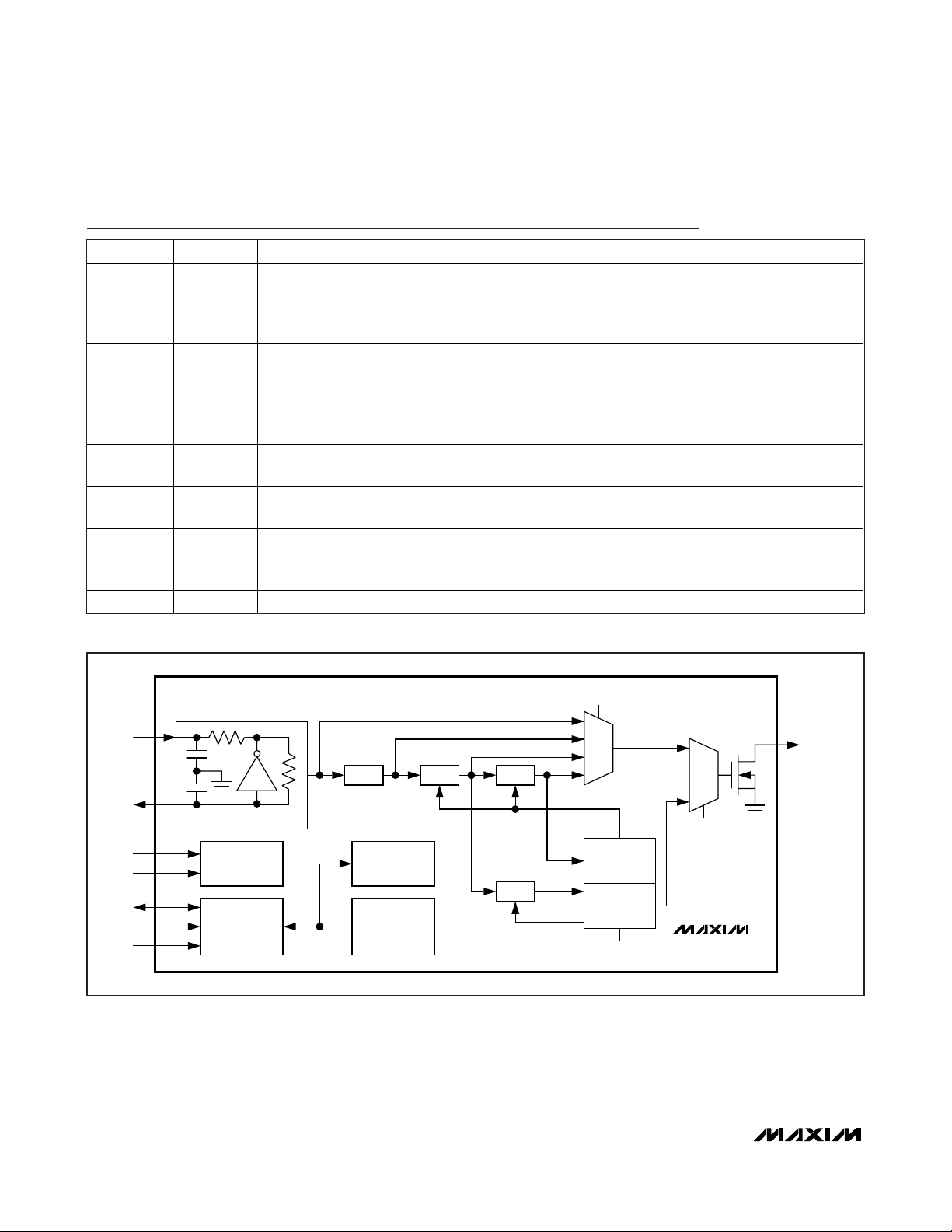
Pin Description
Figure 1. Block Diagram
I2C, 32-Bit, Binary Counter Clock with 64-Bit ID
PIN NAME FUNCTION
Connections for Standard 32.768kHz Quartz Crystal. The internal oscillator circuitry is designed for
1, 2 X1, X2
3 AD0
4 GND Ground
5 SDA
6 SCL
7 SQW/INT
8 VCC DC Power Pin. This pin should be decoupled using a 0.1μF or 1.0μF capacitor.
operation with a crystal having a 12.5pF specified load capacitance (C
oscillator and can optionally be connected to an external 32.768kHz oscillator. The output of the
internal oscillator, pin X2, is floated if an external oscillator is connected to pin X1.
Slave Address Input. This pin is the slave address input for the I
access multiple devices on the same bus. To select the device, the address value on the pin
must match the corresponding bit in the device addresses. This pin can be connected to V
ground or be driven to a log ic-high or logic-low leve l.
Serial Data Input/Output. This pin is the data input/output for the I
open drain and requires an external pullup resistor.
Serial Clock Input. This pin is the clock input for the I
2
C serial interface and is used to synchronize
data movement on the serial interface.
Square Wave or Active-Low Interrupt Open-Drain Output. This pin is used to output the square wave
or alarm interrupt signal. The function of this pin is selected by the state of the INTCN control bit.
Thi s pin is open drain and requires an e xternal pul lup resistor.
). Pin X1 is the input to the
L
2
C serial interface and is used to
2
C serial interface. The SDA pin is
CC
or
X1
V
GND
SDA
SCL
AD0
X2
CC
OSCILLATOR
POWER
I2C
INTERFACE
÷4
CONTROL/
64-BIT ID
STATUS
ROM
RS[2:1]
32,768HzDIVIDER CHAIN
8192Hz
4096Hz
÷2
÷4096
÷4096
1Hz
1Hz
CLR
SQW
MUX
32-BIT
COUNTER
24-BIT ALARM
COUNTER
ACE
AF
MUX
INTCN
DS1372
SQW/INT
N
 Loading...