General Description
The DS1124 is an 8-bit programmable timing element
similar in function to the DS1021-25. The 256-delay
intervals are programmed by using a 3-wire serial interface. With a 0.25ns step size, the DS1124 can provide
a delay time from 20ns up to 84ns with an integral nonlinearity of ±3ns.
Applications
LCD Televisions
Telecommunications
Digital Test Equipment
Digital Video Projection
Signal Generators and Analyzers
Features
♦ 0.25ns Step Size
♦ Leading- and Trailing-Edge Accuracy
♦ CMOS/TTL Compatible
♦ Can Delay Signals by a Full Period or More
♦ 3-Wire Serial Programming Interface
♦ Single 5.0V Power Supply
♦ 10-pin µSOP Package
DS1124
5.0V 8-Bit Programmable
Timing Element
Rev 0; 7/07
+
Denotes a lead-free package.
Ordering Information
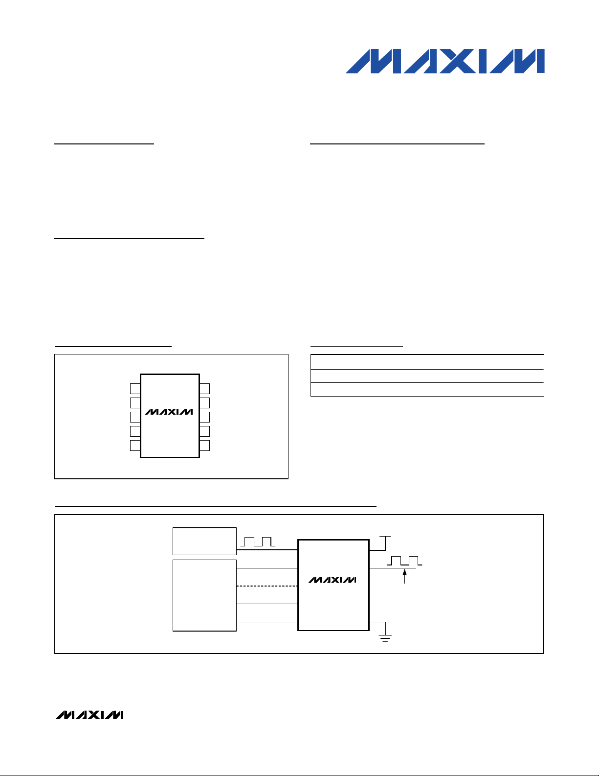
Pin Configuration
GND
OUT
V
CC
E
V
CC
IN
Q
CLK
D
MICROPROCESSOR
SYSTEM CLOCK
OPTIONAL
VARIABLE DELAY
DS1124
Typical Operating Circuit
________________________________________________________________
Maxim Integrated Products
1
For pricing, delivery, and ordering information, please contact Maxim Direct at 1-888-629-4642,
or visit Maxim’s website at www.maxim-ic.com.
TOP VIEW
+
IN
1
E
2
Q
3
DS1124
4
5
10
V
CC
V
9
CC
D
8
CLKGND
7
OUTGND
6
PART TEMP RANGE PIN-PACKAGE
DS1124U-25+ -40°C to +85°C 10 μSOP
DS1124U-25+T -40°C to +85°C 10 μSOP (Tape-and-Reel)
µSOP

ABSOLUTE MAXIMUM RATINGS
RECOMMENDED OPERATING CONDITIONS
(TA= -40°C to +85°C)
Stresses beyond those listed under “Absolute Maximum Ratings” may cause permanent damage to the device. These are stress ratings only, and functional
operation of the device at these or any other conditions beyond those indicated in the operational sections of the specifications is not implied. Exposure to
absolute maximum rating conditions for extended periods may affect device reliability.
Voltage Range on VCCPin Relative to Ground .....-0.5V to +6.0V
Voltage Range on IN, E, D, and CLK
Relative to Ground* ................................-0.5V to (V
CC
+ 0.5V)
Operating Temperature Range ...........................-40°C to +85°C
Storage Temperature Range .............................-55°C to +125°C
Short-Circuit Output Current ..........................50mA for 1 second
Soldering Temperature...................See J-STD-020 Specification
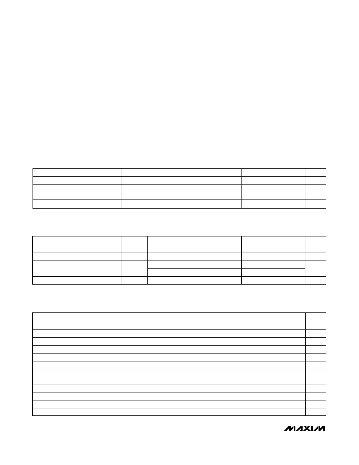
DC ELECTRICAL CHARACTERISTICS
(VCC= +4.75V to +5.25V, TA= -40°C to +85°C, unless otherwise noted.)
AC ELECTRICAL CHARACTERISTICS
(VCC= +4.75V to +5.25V, TA= -40°C to +85°C, unless otherwise noted.)
DS1124
5.0V 8-Bit Programmable
Timing Element
2 _______________________________________________________________________________________
*
Not to exceed +6.0V.
Supply Voltage V
Input Logic 1 V
Input Logic 0 V
PARAMETER SYMBOL CONDITIONS MIN TYP MAX UNITS
(Note 1) 4.75 5.25 V
CC
IH
IL
Active Current I
High-Level Output Current IOH V
Low-Leve l Output Current I
Input Leakage IL -1.0 +1.0 μA
PARAMETER SYMBOL CONDITIONS MIN TYP MAX UNITS
15 30 mA
CCA
= min, V
CC
Q pin, V
OL
OUT pin, V
2.2
-0.3 +0.8 V
= 2.3V -1.0 mA
OH
CC
CC
= min, V
= min, V
= 0.5V 4.0
OL
= 0.5V 8.0
OL
V
+
CC
0.3
V
mA
PARAMETER SYMBOL CONDITIONS MIN TYP MAX UNITS
Serial Clock Frequency f
Input Pulse Width (E, CLK) tEW, tCW 50 ns
Data Setup to C loc k t
Data Hold from Clock t
Data Setup to Enable t
Data Hold to Enable t
Enable Setup to Clock tES 0 ns
Enable Ho ld from Clock tEH 30 ns
E to Q Valid t
E to Q High Impedance t
CLK to Q Valid t
CLK to Q Invalid t
10 MHz
CLK
30 ns
DSC
0 ns
DHC
30 ns
DSE
0 ns
DHE
50 ns
EQV
0 50 ns
EQZ
50 ns
CQV
0 ns
CQX

DS1124
5.0V 8-Bit Programmable
Timing Element
_______________________________________________________________________________________ 3
Note 1: All voltages are referenced to ground.
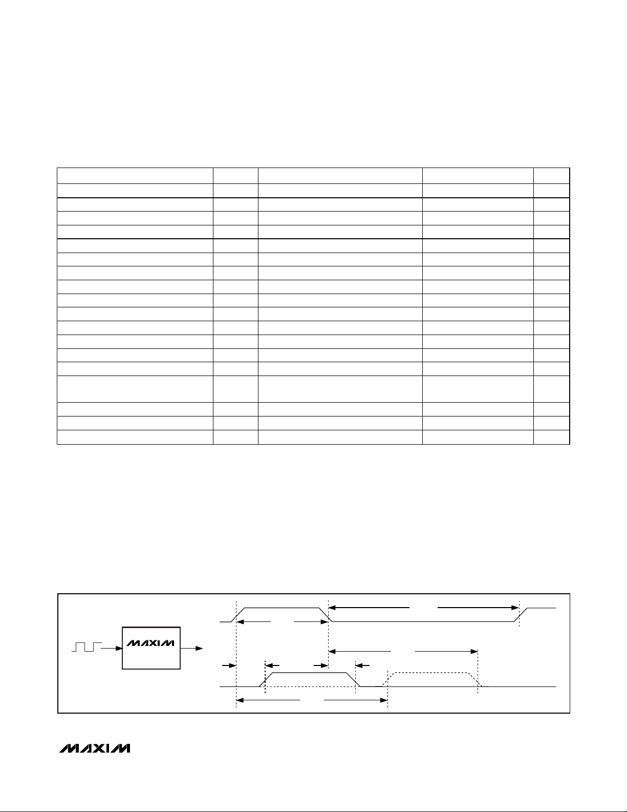
Note 2: Measured from rising edge of the input to the rising edge of the output. The programmed delay, t
D
, can be programmed
with values from 0 to 255. See Figure 1.
Note 3: See the
Integral Nonlinearity
section and Figure 6.
Note 4: This is the minimum allowable interval between transitions on the input to ensure accurate device operation. This parameter
can be violated but timing accuracy may be impaired and ultimately very narrow pulse widths will result in no output from
the device. See Figure 1.
Note 5: When a 50% duty cycle input clock is used, this defines the highest usable clock frequency. When asymmetrical clock
inputs are used, the maximum usable clock frequency must be reduced to conform to the minimum input pulse-width
requirement. See Figure 1.
Note 6: Faster rise and fall times give the greatest accuracy in measured delay. Slow edges (outside the specification maximum)
can result in erratic operations.
AC ELECTRICAL CHARACTERISTICS (continued)
(VCC= +4.75V to +5.25V, TA= -40°C to +85°C, unless otherwise noted.)
Figure 1. Delay Timing Diagram
E to Delay Val id t
E to Delay Invalid t
Power-Up Time tPU 100 ms
Delay Step Size t
Step 0 Delay TD0 (Note 2) 17 20 23 ns
Step 0 Delay Initial Accuracy VCC = 5V, TA = +25°C -0.6 +0.6 ns
Step 0 Voltage Variation -0.4 +0.4 ns
Step 0 Temperature Variation 0°C to +70°C -1 +1 ns
Step 0 Temperature Variation -40°C to +85°C -1 +1 ns
Step 255 Delay T
Step 255 Delay Initial Accuracy VCC = 5V, TA = +25°C -0.6 +0.6 ns
Step 255 Voltage Variat ion -0.4 +0.4 ns
Step 255 Temperature Variation 0°C to +70°C -3 +3 ns
Step 255 Temperature Variation -40°C to +85°C -5 +5 ns
Integral Nonlinearity
(Deviation from Straight Line)
Minimum Input Pulse Width tWI (Note 4) 40 ns
Minimum Input Period t
Input Ri se and Fall Times tR, tF (Note 6) 0 1 μs
PARAMETER SYMBOL CONDITIONS MIN TYP MAX UNITS
50 μs
EDV
0 ns
EDX
TA= +25°C -0.75 +0.25 +1 ns
STEP
(Note 2) 77 83.75 88 ns
D255
TA= +25°C (Note 3) -2 0 +2 ns
t
ERR
(Note 5) 80 ns
PER
t
WI
t
WI
t
D
D0
t
D0
t
D
IN
DS1124
TIMING REFERENCED TO 1.5V.
IN
OUT
t
OUT
 Loading...