Maxim Integrated Producs DS1081LE+T, DS1081 Datasheet

General Description
The DS1081L is a spread-spectrum clock modulator IC
that reduces EMI in high clock-frequency-based, digital
electronic equipment.
Using an integrated phase-locked loop (PLL), the
DS1081L accepts an input clock signal in the range of
20MHz to 134MHz and delivers a spread-spectrum modulated output clock signal. The PLL modulates, or dithers,
the output clock about the center input frequency at a
pin-selectable magnitude and dither rate, allowing direct
EMI control and optimization. In addition, through an
enable pin the dithering can be enabled or disabled for
easy comparison of system performance during EMI testing. This same input pin also allows the DS1081L output
to be tri-stated.
By dithering the system clock, all the address, data,
and timing signals generated from this signal are also
dithered so that the measured EMI at the fundamental
and harmonic frequencies is greatly reduced. This is
accomplished without changing clock rise/fall times or
adding the space, weight, design time, and cost associated with mechanical shielding.
The DS1081L is provided in an 8-pin TSSOP package
and operates over a full automotive temperature range
of -40°C to +125°C.
Applications
LCD Panels for TVs, Desktop Monitors, and
Notebook and Tablet PCs
Automotive Telematics and Infotainment
Printers
Features
♦ Modulates a 20MHz to 134MHz Clock with Center
Spread-Spectrum Dithering
♦ Selectable Spread-Spectrum Modulation
Magnitudes of:
±0.5%
±1.0%
±1.5%
±2.0%
♦ Low 75ps Cycle-to-Cycle Jitter
♦ Spread-Spectrum Disable Mode
♦ Pin Compatible with Alliance/PulseCore
Semiconductor P2040 Series Devices
♦ Clock Output Disable
♦ Low Cost
♦ Low Power Consumption
♦ 3.3V Single Voltage Supply
♦ -40°C to +125°C Temperature Range
♦ Small 8-Pin TSSOP Package
DS1081L
20MHz to 134MHz Spread-Spectrum
Clock Modulator for LCD Panels
______________________________________________
Maxim Integrated Products
1
Rev 0; 4/07
For pricing, delivery, and ordering information, please contact Maxim/Dallas Direct! at
1-888-629-4642, or visit Maxim’s website at www.maxim-ic.com.
+
Denotes lead-free package.
T
Denotes tape-and-reel.
Ordering Information
PART TEMP RANGE PIN-PACKAGE
DS1081LE+ -40°C to +125°C 8 TSSOP
DS1081LE+T -40°C to +125°C 8 TSSOP
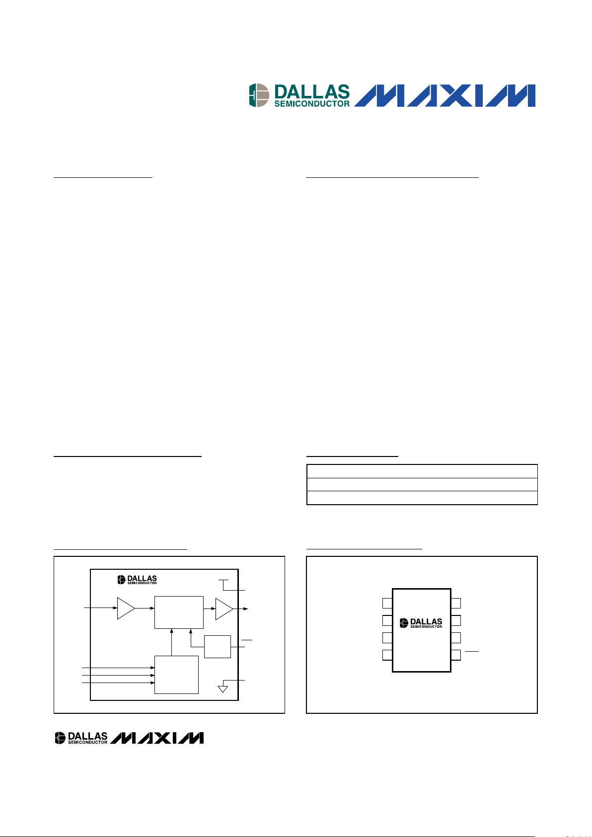
Block Diagram
GND
SSO
PLL WITH CENTER-
DITHERED
SPREAD
SPECTRUM
CONFIGURATION
DECODE AND
CONTROL
SMSEL1
CLKIN
SMSEL2
f
SSO
= 20MHz to
134MHz (DITHERED)
V
CC
V
CC
fIN = 20MHz TO
134MHz
DS1081L
CRSEL
SSEN
ENABLE
LOGIC
Pin Configuration and Typical Operating Circuit appear at
end of data sheet.
SSO
GND
1
2
8
7 CRSELSMSEL1
SMSEL2
CLKIN
TSSOP
(4.40mm)
TOP VIEW
3
4
6
5
DS1081L
V
CC
SSEN
Pin Configuration

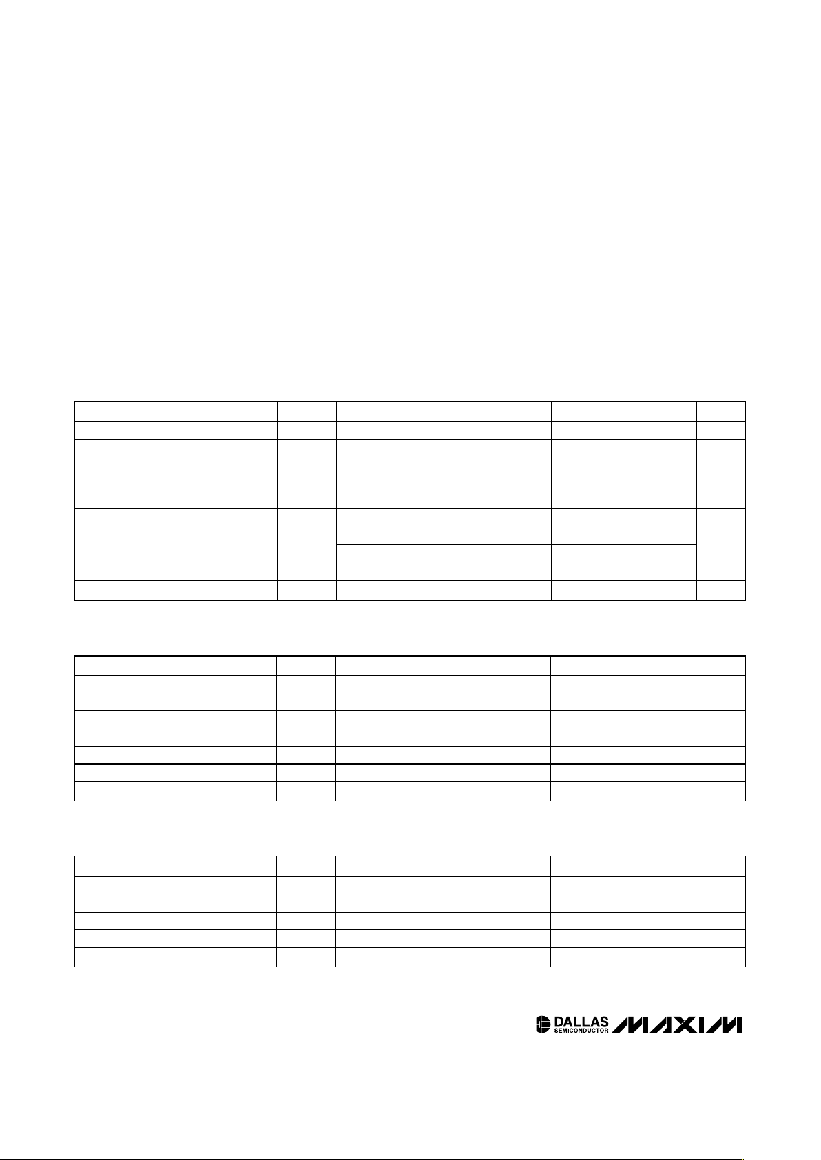
ABSOLUTE MAXIMUM RATINGS
RECOMMENDED OPERATING CONDITIONS
(TA= -40°C to +125°C, unless otherwise noted.)
Stresses beyond those listed under “Absolute Maximum Ratings” may cause permanent damage to the device. These are stress ratings only, and functional
operation of the device at these or any other conditions beyond those indicated in the operational sections of the specifications is not implied. Exposure to
absolute maximum rating conditions for extended periods may affect device reliability.
Voltage Range on VCCRelative to GND .............-0.5V to +3.63V
Voltage Range on Any Lead Relative
to GND ................-0.5V to (V
CC
+ 0.5V), not to exceed +3.63V
Operating Temperature Range .........................-40°C to +125°C
Storage Temperature Range .............................-55°C to +125°C
Soldering Temperature...................See J-STD-020 Specification
PARAMETER SYMBOL CONDITIONS MIN TYP MAX UNITS
Supply Voltage VCC (Note 1) 3.0 3.6 V
Input Logic 1 V
IH
0.8 x
V
CC
VCC +
0.3
V
Input Logic 0 VIL -0.3
0.2 x
V
CC
V
Input Logic Float (SSEN, CRSEL) V
FLOAT
0V < VIN < VCC ±1 μA
SSO < 80MHz 15
SSO Load C
L
80MHz SSO < 134MHz 7
pF
CLKIN Frequency fIN 20 134 MHz
CLKIN Duty Cycle f
INDC
40 60 %
DC ELECTRICAL CHARACTERISTICS
(VCC= +3.0V to +3.6V, TA= -40°C to +125°C, unless otherwise noted.)
PARAMETER SYMBOL CONDITIONS MIN TYP MAX UNITS
Supply Current I
CC
CL = 7pF
f
IN
= 134MHz
15 mA
SMSEL1/SMSEL2/CLKIN Input Leakage I
IL:1
0V < VIN < VCC -1 +1 μA
CRSEL/SSEN Input Leakage I
IL:2
0V < VIN < VCC -100 +100 μA
Output Leakage (SSO) I
OZ
SSEN = float -1 +1 μA
Low-Leve l Output Voltage (SSO) VOL IOL = 4mA 0.4 V
High-Level Output Voltage (SSO) VOH IOH = -4mA 2.4 V
AC ELECTRICAL CHARACTERISTICS
(VCC= +3.0V to +3.6V, TA= -40°C to +125°C, unless otherwise noted.)
PARAMETER SYMBOL CONDITIONS MIN TYP MAX UNITS
SSO Duty Cycle f
SSODC
Measured at VCC/2 40 60 %
SSO Ri se Time tR CL = 7pF 1 ns
SSO Fal l T ime tF CL = 7pF 1 ns
Peak Cycle-to-Cycle Jitter tJ TA = -40°C to +85°C, 10,000 cyc les 75 ps
Power-Up Time t
POR
(Note 2) 50 m s
DS1081L
20MHz to 134MHz Spread-Spectrum
Clock Modulator for LCD Panels
2 _____________________________________________________________________
Note 1: All voltages referenced to ground. Currents into the IC are positive and out of the IC are negative.
Note 2: Time between power applied to device and stable output.
 Loading...