

Page 1
For pricing, delivery, and
ordering information, please contact Maxim Direct
at 1-888-629-4642, or visit Maxim’s website at www.maxim
integrated
.com.
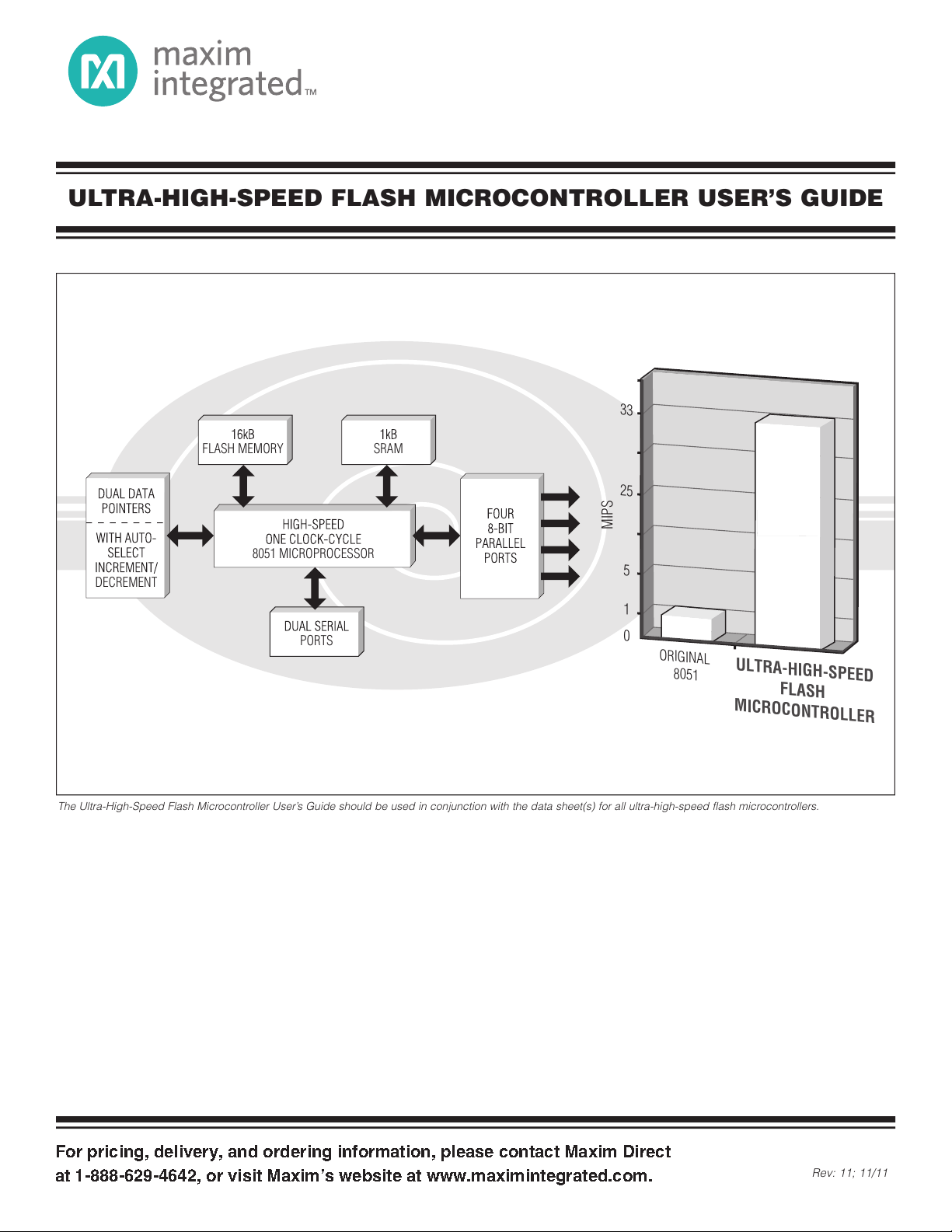
DECREMENT
PORTS
8051 MICROPROCESSOR
FLASH MEMORY SRAM
1
5
25
0
33
ULTRA-HIGH-SPEED
FLASH
MICROCONTROLLER
ORIGINAL
8051
MIPS
ULTRA-HIGH-SPEED FLASH MICROCONTROLLER USER’S GUIDE
The Ultra-High-Speed Flash Microcontroller User’s Guide should be used in conjunction with the data sheet(s) for all ultra-high-speed flash microcontrollers.
Rev: 11; 11/11
Page 2

Ultra-High-Speed Flash
REVI S ION
NUMBER
REVI S ION
DATE
SECTION
NUMBER
DESCRIPTION
PAGES
CHANGED
0 1/01 — Init i a l relea se. —
1 10/02 — Corrected some t ypo s.
2 12/02 — Changed title to refle ct “ f las h ” and removed “DS89C 42 0 ” referenc e. Al l
3 8/03 — Made documen t un iver s a l to a l l Dal l a s u ltr a-h igh-speed mi cro co ntro l lers. Al l
4 Clarif i ed t hat t h e C T M bit is c leared in stop mode. 14
5 Corrected cycle time s for ADDC A, R n instr uc t io n . 50
4 2/04
15 In the C o m ma nd Summar ies secti o n , c larifi ed t ha t PMR SFR i s not disp la yed i n ROM loader. 133
5 8/04 4 Added FCNTL and FDATA to the Specia l-Fu n ct i o n Regis t er Lo ca t io n s tabl e. 14, 15
6 12/04 15 Changed the ACK /N A K re sp on ses in th e Co mmand Summar ie s sec t io n . 136
15
In the Com ma nd Summ ar ie s se c t i o n , c l ar ified tha t th e boot loader K co m ma nd does not erase t h e opt ion
control regi ster, whic h co ntr o l s the defaul t state o f t h e en ab le watchdog tim er bit.
136
15
Remo ved infor mat ion pertain ing to the paral lel programming m ode and inst e ad referred interest ed partie s to
contact microcon tro l ler t ec h n i c a l sup port directl y for more informa t io n .
138
7 10/05
4 Added Rev i sio n ID SFR. 14, 15, 26
12 Cl ari f i ed t he sele c t i o n of the sh ift c lo ck frequenc y for Mode 0 (fir st paragraph, last sent en c e). 116
8 3/07
14
In Instr uct ion Set Deta i l s for the D at a Tr an sf er tab le secti o n , changed "=" to " " for XCH A, Rn ; XCH a, direct;
XCH A, @R i ; and XCHD A, @R i; and changed ORLC, bit (72h) D7 from 1 to 0 in the Bo o lea n Variab le
Manipu l a t ion tab le sect i o n ; ch a nged the i n structi o n code for JZ rel (60h) D7 from 1 to 0 and D6 and D5 from
0 to 1 and for JNZ rel (70h) D7 from 1 to 0 and D6, D5, and D4 from 0 to 1; ch anged the JNB bi t, re l (30h) D5
from 0 to 1 and CJ NE A, d irect, r e l (B5 h) D6 from 0 to 1.
128, 12 9,
130
9 6/07 4 Corrected bi t na m e headings f or the R MS[2:0] tab le . 32
10 3/08 4 Corrected formatting errors. 23, 24
11 11/11 4 Corrected the T i m er 1 a nd 0 bit d e scr iptions for the CKMOD regist er ( swapped 1 and 0 for respecti ve t im er s) 4–21
Microcontroller User’s Guide
REVISION HISTORY
Maxim cannot assume responsibility for use of any circuitry other than circuitry entirely embodied in a Maxim product. No circuit patent licenses are implied. Maxim reserves the right to change the
circuitry and specifications without notice at any time.
Maxim Integrated Products, 120 San Gabriel Drive, Sunnyvale, CA 94086 408-737-7600 _______________________________________________________ 1
© 2011 Maxim Integrated Products is a registered trademark of Maxim Integrated Products, Inc.
Page 3

Ultra-High-Speed Flash
Microcontroller User’s Guide
SECTION 1: INTRODUCTION
Maxim’s ultra-high-speed flash microcontroller is an 8051-compatible microcontroller that provides improved performance and power
consumption when compared to the original 8051 version. It retains instruction set and object code compatibility with the 8051, yet performs the same operations in fewer clock cycles. Consequently, greater throughput is possible for the same crystal speed. As an alternative, the device can be run at a reduced frequency to save power. The more efficient design allows a much slower crystal speed to
get the same results as an original 8051, using much less power.
The fundamental innovation of the ultra-high-speed flash microcontroller is the use of only one clock per instruction cycle compared
with 12 for the original 8051. This results in up to 12 times improvement in performance over the original 8051 architecture and up to
four times improvement over other Maxim high-speed microcontrollers. The device provides several peripherals and features in addition to all of the standard features of an 80C32. These include 16kB/32kB/64kB of on-chip flash memory, 1kB of on-chip RAM, four 8-bit
I/O ports, three 16-bit timer/counters, two on-chip UARTs, dual data pointers, an on-chip watchdog timer, five levels of interrupt priority,
and a crystal multiplier. The device provides 256 bytes of RAM for variables and stack; 128 bytes can be reached using direct or indirect
addressing, or using indirect addressing only.
In addition to improved efficiency, it can operate at a maximum clock rate of 33MHz. Combined with the 12 times performance, this
allows for a maximum performance of 33 million instructions per second (MIPS). This level of computing power is comparable to many
16-bit processors, but without the added expense and complexity if implementing a 16-bit interface.
The device incorporates a power-management mode that allows the device to dynamically vary the internal clock speed from 1 clock
per cycle (default) to 1024 clocks per cycle. Because power consumption is directly proportional to clock speed, the device can reduce
its operating frequency during periods of little switchback. This greatly reduces power consumption. The switchback feature allows the
device to quickly return to highest speed operation upon receipt of an interrupt or serial port activity, allowing the device to respond to
external events while in power-management mode.
Maxim Integrated
1-1
Page 4

Ultra-High-Speed Flash
Microcontroller User’s Guide
SECTION 2: ORDERING INFORMATION
The ultra-high-speed flash microcontroller family follows the part numbering convention shown below. Note that not all combinations of
devices may be currently available. Contact a Maxim sales office for up-to-date details.
DS89C420-QCL
SPEED: L 33MHz
TEMPERATURE: C 0°C to +70°C
N -40°C to+85°C
M PDIP
PACKAGE: Q PLCC
E Thin Quad Flat Pack (TQFP)
OPERATING VOLTAGE: 0 +5V
MEMORY TYPE: 9 Flash
Maxim Integrated
2-1
Page 5

Ultra-High-Speed Flash
Microcontroller User’s Guide
SECTION 3: ARCHITECTURE
This section contains the following information:
ALU . . . . . . . . . . . . . . . . . . . . . . . . . . . . . . . . . . . . . . . . . . . . . . . . . . . . . . . . . . . . . . . . . . . . . . . . .3-2
Special-Function Registers . . . . . . . . . . . . . . . . . . . . . . . . . . . . . . . . . . . . . . . . . . . . . . . . . . . . . . .3-2
Accumulator . . . . . . . . . . . . . . . . . . . . . . . . . . . . . . . . . . . . . . . . . . . . . . . . . . . . . . . . . . . . . .3-2
B Register . . . . . . . . . . . . . . . . . . . . . . . . . . . . . . . . . . . . . . . . . . . . . . . . . . . . . . . . . . . . . . . .3-2
Program Status Word . . . . . . . . . . . . . . . . . . . . . . . . . . . . . . . . . . . . . . . . . . . . . . . . . . . . . . .3-2
Data Pointer(s) . . . . . . . . . . . . . . . . . . . . . . . . . . . . . . . . . . . . . . . . . . . . . . . . . . . . . . . . . . . .3-2
Stack Pointer . . . . . . . . . . . . . . . . . . . . . . . . . . . . . . . . . . . . . . . . . . . . . . . . . . . . . . . . . . . . .3-2
I/O Ports . . . . . . . . . . . . . . . . . . . . . . . . . . . . . . . . . . . . . . . . . . . . . . . . . . . . . . . . . . . . . . . . .3-2
Timer/Counters . . . . . . . . . . . . . . . . . . . . . . . . . . . . . . . . . . . . . . . . . . . . . . . . . . . . . . . . . . . .3-2
UARTs . . . . . . . . . . . . . . . . . . . . . . . . . . . . . . . . . . . . . . . . . . . . . . . . . . . . . . . . . . . . . . . . . . .3-2
Scratchpad Registers (RAM) . . . . . . . . . . . . . . . . . . . . . . . . . . . . . . . . . . . . . . . . . . . . . . . . . . . . .3-3
Stack . . . . . . . . . . . . . . . . . . . . . . . . . . . . . . . . . . . . . . . . . . . . . . . . . . . . . . . . . . . . . . . . . . . .3-3
Working Registers . . . . . . . . . . . . . . . . . . . . . . . . . . . . . . . . . . . . . . . . . . . . . . . . . . . . . . . . .3-3
Program Counter . . . . . . . . . . . . . . . . . . . . . . . . . . . . . . . . . . . . . . . . . . . . . . . . . . . . . . . . . .3-3
Address/Data Bus . . . . . . . . . . . . . . . . . . . . . . . . . . . . . . . . . . . . . . . . . . . . . . . . . . . . . . . . .3-3
Watchdog Timer . . . . . . . . . . . . . . . . . . . . . . . . . . . . . . . . . . . . . . . . . . . . . . . . . . . . . . . . . . .3-3
Power Monitor . . . . . . . . . . . . . . . . . . . . . . . . . . . . . . . . . . . . . . . . . . . . . . . . . . . . . . . . . . . . .3-3
Interrupts . . . . . . . . . . . . . . . . . . . . . . . . . . . . . . . . . . . . . . . . . . . . . . . . . . . . . . . . . . . . . . . .3-3
Timing Control . . . . . . . . . . . . . . . . . . . . . . . . . . . . . . . . . . . . . . . . . . . . . . . . . . . . . . . . . . . .3-3
Flash Memory . . . . . . . . . . . . . . . . . . . . . . . . . . . . . . . . . . . . . . . . . . . . . . . . . . . . . . . . . . . . . . . . .3-4
3-1
Maxim Integrated
Page 6

Ultra-High-Speed Flash
Microcontroller User’s Guide
SECTION 3: ARCHITECTURE
The architecture is based on the industry-standard 87C52 and executes the standard 8051 instruction set. The core is an accumulator-based architecture using internal registers for data storage and peripheral control. This section provides a brief description of each
architecture feature. Details concerning the programming model, instruction set, and register description are provided in Section 4.
ALU
The ALU is responsible for math functions, comparisons, and general decision making. The ALU is not used explicitly by software.
Instruction decoding prepares the ALU automatically and passes it the appropriate data. The ALU primarily uses two special-function
registers (SFRs) as the source and destination for all operations. These are the accumulator and B register. The ALU also provides status information in the program status register. The SFRs are described in the following pages.
Special-Function Registers
All peripherals and operations that are not explicitly controlled by instructions are controlled through SFRs. All SFRs are described in
Section 4. The most commonly used registers that are basic to the architecture are also described in the following pages.
Accumulator
The accumulator is a source and destination for many operations involving math, data movement, and decisions. Although it can be
bypassed, most high-speed instructions require the use of the accumulator (A or ACC) as one argument.
B Register
The B register is used as the second 8-bit argument in multiply and divide operations. When not used for these purposes, the B register can be used as a general-purpose register.
Program Status Word
The program status word holds a selection of bit flags that include the carry flag, auxiliary carry flag, general-purpose flag, register
bank select, overflow flag, and parity flag.
Data Pointer(s)
The data pointers (DPTR and DPTR1) are used to assign a memory address for the MOVX instructions. This address can point to a
data memory location, either on- or off-chip, or a memory-mapped peripheral. When moving data from one memory area to another or
from memory to a memory-mapped peripheral, a pointer is needed for both the source and destination. The user can select the active
pointer through a dedicated SFR bit (Sel = DPS.0), or can activate an automatic toggling feature for altering the pointer selection (TSL
= DPS.5). An additional feature, if selected, provides automatic incrementing or decrementing of the current DPTR.
Stack Pointer
The stack pointer denotes the register location at the top of the stack, which is the last used value. The user can place the stack anywhere in the scratchpad RAM by setting the stack pointer to the desired location, although the lower bytes are normally used for working registers.
I/O Ports
Four 8-bit I/O ports are available. Each I/O port is represented by an SFR location, and can be written or read. The I/O port has a latch
that contains the value written by software. In general, software reads the state of external pins during a read operation.
Timer/Counters
Three 16-bit timer/counters are available. Each timer is contained in two SFR locations that can be written or read by software. The
timers are controlled by other SFRs described in Section 4.
UARTs
The two UARTs are controlled and accessed by SFRs. Each UART has an address that is used to read and write the UART. The same
address is used for both read and write operations, which are distinguished by the instruction. Each UART is controlled by its own SFR
control register.
Maxim Integrated
Page 7

Ultra-High-Speed Flash
Microcontroller User’s Guide
Scratchpad Registers (RAM)
The high-speed core provides 256 bytes of scratchpad RAM for general-purpose data and variable storage. The first 128 bytes are
directly available to software. The second 128 are available through indirect addressing. Selected portions of this RAM have other
optional functions.
Stack
The stack is a RAM area that stores return address information during calls and interrupts. The user can also place variables on the
stack when necessary. The stack pointer designates the RAM location that is the top of the stack. Thus, depending on the value of the
stack pointer, the stack can be located anywhere in the 256 bytes of RAM. A common location would be in the upper 128 bytes of
RAM, as these locations are accessible through indirect addressing only.
Working Registers
The first 32 bytes of the scratchpad RAM can be used as four banks of eight working registers for high-speed data movement. Using
four banks, software can quickly change context by changing to a different bank. In addition to the accumulator, the working registers
are commonly used as data source or destination. Some of the working registers can also be used as pointers to other RAM locations
(indirect addressing).
Program Counter
The program counter (PC) is a 16-bit value that designates the next program address to be fetched. On-chip hardware automatically
increments the PC value to move to the next program memory location.
Address/Data Bus
The device addresses a 64kB program and 64kB data memory area that resides in a combination of internal and external memory. When
external memory is accessed, ports 0 and 2 are used as a multiplexed address and data bus. Three external memory bus structures
are supported. The nonpage mode (traditional 8051) bus structure provides the address MSB on port 2 and multiplexes port 0 between
address LSB and data. The page mode 1 bus structure uses port 0 exclusively for data and multiplexes port 2 between address MSB
and address LSB. The page mode 2 bus structure uses port 0 exclusively for address LSB and multiplexes port 2 between address MSB
and data. These addressing modes are detailed later.
Watchdog Timer
The watchdog timer provides a supervisory function for applications that cannot afford to run out of control. The watchdog timer is a
programmable, free-running timer. If allowed to reach the termination of its count, if enabled, the watchdog resets the CPU software
must prevent this by clearing or resetting the watchdog prior to its timeout.
Power Monitor
A bandgap reference and analog circuitry are incorporated to monitor the power-supply conditions. When VCCbegins to drop out of
tolerance, the power monitor issues an optional early warning power-fail interrupt. If power continues to fall, the power monitor invokes
a reset condition. This remains until power returns to normal operating voltage. The power monitor also functions on power-up, holding the microcontroller in a reset state until power is stable.
Interrupts
The device is capable of evaluating 13 interrupt sources simultaneously. Each interrupt has an associated interrupt vector, flag, priority, and enable. These interrupts can be globally enabled or disabled.
Timing Control
The microcontroller provides an on-chip oscillator for use with an external crystal. This can be bypassed by injecting a clock source
into the XTAL1 pin. The clock source is used to create machine cycle timing (four clocks), ALE, PSEN, watchdog, timer, and serial baudrate timing. In addition, an on-chip ring oscillator can be used to provide an approximately 10MHz clock source. A frequency multiplier feature is included, which can be selected by SFR control to multiply the input clock source by either two or four. This allows lower
frequency (and cost) crystals to be used while still allowing internal operation up to the full 33MHz limit.
3-3
Maxim Integrated
Page 8

Ultra-High-Speed Flash
Microcontroller User’s Guide
Flash Memory
On-chip program memory is implemented in flash memory. This can be programmed in-system with the standard 5V VCCsupply
through a serial port (in-system) using a built-in program memory loader, or by a standard flash or EPROM programmer. Full programming details are given in Section 15.
A memory management unit (MMU) and other hardware supports any of the three programming methods. The MMU controls program
and data memory access, and provides sequencing and timing controls for programming of the on-chip program memory
also a separate security flash block that is used to support a standard three-level lock, a 64-byte encryption array, and other flash
options.
The full on-chip program memory range can be fetched by the processor automatically. Reset routines and all interrupt vectors are
located in the lower 128 bytes of the on-chip program memory area.
. There is
Maxim Integrated
Page 9

Ultra-High-Speed Flash
Microcontroller User’s Guide
SECTION 4: PROGRAMMING MODEL
This section contains the following information:
Memory Organization . . . . . . . . . . . . . . . . . . . . . . . . . . . . . . . . . . . . . . . . . . . . . . . . . . . . . . . . . . .4-5
Memory Map . . . . . . . . . . . . . . . . . . . . . . . . . . . . . . . . . . . . . . . . . . . . . . . . . . . . . . . . . . . . . . . . .4-5
Register Map . . . . . . . . . . . . . . . . . . . . . . . . . . . . . . . . . . . . . . . . . . . . . . . . . . . . . . . . . . . . . . . . .4-5
Bit Addressable Locations . . . . . . . . . . . . . . . . . . . . . . . . . . . . . . . . . . . . . . . . . . . . . . . . . . . . . . .4-7
Working Registers . . . . . . . . . . . . . . . . . . . . . . . . . . . . . . . . . . . . . . . . . . . . . . . . . . . . . . . . . . . . .4-7
Stack . . . . . . . . . . . . . . . . . . . . . . . . . . . . . . . . . . . . . . . . . . . . . . . . . . . . . . . . . . . . . . . . . . . . . . . .4-7
Addressing Modes . . . . . . . . . . . . . . . . . . . . . . . . . . . . . . . . . . . . . . . . . . . . . . . . . . . . . . . . . . . . .4-7
Register Addressing . . . . . . . . . . . . . . . . . . . . . . . . . . . . . . . . . . . . . . . . . . . . . . . . . . . . . . . .4-8
Direct Addressing . . . . . . . . . . . . . . . . . . . . . . . . . . . . . . . . . . . . . . . . . . . . . . . . . . . . . . . . . .4-8
Register Indirect Addressing . . . . . . . . . . . . . . . . . . . . . . . . . . . . . . . . . . . . . . . . . . . . . . . . .4-8
Immediate Addressing . . . . . . . . . . . . . . . . . . . . . . . . . . . . . . . . . . . . . . . . . . . . . . . . . . . . . .4-9
Register Indirect with Displacement . . . . . . . . . . . . . . . . . . . . . . . . . . . . . . . . . . . . . . . . . . .4-9
Relative Addressing . . . . . . . . . . . . . . . . . . . . . . . . . . . . . . . . . . . . . . . . . . . . . . . . . . . . . . . .4-9
Page Addressing . . . . . . . . . . . . . . . . . . . . . . . . . . . . . . . . . . . . . . . . . . . . . . . . . . . . . . . . . .4-9
Extended Addressing . . . . . . . . . . . . . . . . . . . . . . . . . . . . . . . . . . . . . . . . . . . . . . . . . . . . . . .4-9
Program Status Flags . . . . . . . . . . . . . . . . . . . . . . . . . . . . . . . . . . . . . . . . . . . . . . . . . . . . . . . . . . .4-10
Special-Function Register Locations . . . . . . . . . . . . . . . . . . . . . . . . . . . . . . . . . . . . . . . . . . . . . . .4-10
Special-Function Registers . . . . . . . . . . . . . . . . . . . . . . . . . . . . . . . . . . . . . . . . . . . . . . . . . . . . . . .4-13
Port 0 (P0) . . . . . . . . . . . . . . . . . . . . . . . . . . . . . . . . . . . . . . . . . . . . . . . . . . . . . . . . . . . . . . .4-13
Stack Pointer (SP) . . . . . . . . . . . . . . . . . . . . . . . . . . . . . . . . . . . . . . . . . . . . . . . . . . . . . . . . . .4-13
Data Pointer Low 0 (DPL) . . . . . . . . . . . . . . . . . . . . . . . . . . . . . . . . . . . . . . . . . . . . . . . . . . . .4-13
Data Pointer High 0 (DPH) . . . . . . . . . . . . . . . . . . . . . . . . . . . . . . . . . . . . . . . . . . . . . . . . . . .4-14
Data Pointer Low 1 (DPL1) . . . . . . . . . . . . . . . . . . . . . . . . . . . . . . . . . . . . . . . . . . . . . . . . . . .4-14
Data Pointer High 1 (DPH1) . . . . . . . . . . . . . . . . . . . . . . . . . . . . . . . . . . . . . . . . . . . . . . . . . .4-14
Data Pointer Select (DPS) . . . . . . . . . . . . . . . . . . . . . . . . . . . . . . . . . . . . . . . . . . . . . . . . . . .4-14
Power Control (PCON) . . . . . . . . . . . . . . . . . . . . . . . . . . . . . . . . . . . . . . . . . . . . . . . . . . . . . .4-15
Timer/Counter Control (TCON) . . . . . . . . . . . . . . . . . . . . . . . . . . . . . . . . . . . . . . . . . . . . . . . .4-16
4-1
Maxim Integrated
Page 10

Ultra-High-Speed Flash
Microcontroller User’s Guide
Timer Mode Control (TMOD) . . . . . . . . . . . . . . . . . . . . . . . . . . . . . . . . . . . . . . . . . . . . . . . . .4-17
Timer 0 LSB (TL0) . . . . . . . . . . . . . . . . . . . . . . . . . . . . . . . . . . . . . . . . . . . . . . . . . . . . . . . . .4-17
Timer 1 LSB (TL1) . . . . . . . . . . . . . . . . . . . . . . . . . . . . . . . . . . . . . . . . . . . . . . . . . . . . . . . . .4-18
Timer 0 MSB (TH0) . . . . . . . . . . . . . . . . . . . . . . . . . . . . . . . . . . . . . . . . . . . . . . . . . . . . . . . .4-18
Timer 1 MSB (TH1) . . . . . . . . . . . . . . . . . . . . . . . . . . . . . . . . . . . . . . . . . . . . . . . . . . . . . . . . .4-18
Clock Control (CKCON) . . . . . . . . . . . . . . . . . . . . . . . . . . . . . . . . . . . . . . . . . . . . . . . . . . . . .4-18
Port 1 (P1) . . . . . . . . . . . . . . . . . . . . . . . . . . . . . . . . . . . . . . . . . . . . . . . . . . . . . . . . . . . . . . .4-20
External Interrupt Flag (EXIF) . . . . . . . . . . . . . . . . . . . . . . . . . . . . . . . . . . . . . . . . . . . . . . . . .4-20
Timer and Serial Port Clock Mode Register (CKMOD) . . . . . . . . . . . . . . . . . . . . . . . . . . . . .4-21
Serial Port 0 Control (SCON0) . . . . . . . . . . . . . . . . . . . . . . . . . . . . . . . . . . . . . . . . . . . . . . . .4-22
Serial Data Buffer 0 (SBUF0) . . . . . . . . . . . . . . . . . . . . . . . . . . . . . . . . . . . . . . . . . . . . . . . . .4-23
Revision ID (RID) . . . . . . . . . . . . . . . . . . . . . . . . . . . . . . . . . . . . . . . . . . . . . . . . . . . . . . . . . .4-23
Address Control (ACON) . . . . . . . . . . . . . . . . . . . . . . . . . . . . . . . . . . . . . . . . . . . . . . . . . . . .4-23
Port 2 (P2) . . . . . . . . . . . . . . . . . . . . . . . . . . . . . . . . . . . . . . . . . . . . . . . . . . . . . . . . . . . . . . .4-24
Interrupt Enable (IE) . . . . . . . . . . . . . . . . . . . . . . . . . . . . . . . . . . . . . . . . . . . . . . . . . . . . . . . .4-24
Slave Address Register 0 (SADDR0) . . . . . . . . . . . . . . . . . . . . . . . . . . . . . . . . . . . . . . . . . . .4-25
Slave Address Register 1 (SADDR1) . . . . . . . . . . . . . . . . . . . . . . . . . . . . . . . . . . . . . . . . . . .4-25
Port 3 (P3) . . . . . . . . . . . . . . . . . . . . . . . . . . . . . . . . . . . . . . . . . . . . . . . . . . . . . . . . . . . . . . .4-25
Interrupt Priority 1 (IP1) . . . . . . . . . . . . . . . . . . . . . . . . . . . . . . . . . . . . . . . . . . . . . . . . . . . . .4-26
Interrupt Priority 0 (IP0) . . . . . . . . . . . . . . . . . . . . . . . . . . . . . . . . . . . . . . . . . . . . . . . . . . . . .4-27
Slave Address Mask Enable Register 0 (SADEN0) . . . . . . . . . . . . . . . . . . . . . . . . . . . . . . . .4-27
Slave Address Mask Enable Register 1 (SADEN1) . . . . . . . . . . . . . . . . . . . . . . . . . . . . . . . .4-28
Serial Port 1 Control (SCON1) . . . . . . . . . . . . . . . . . . . . . . . . . . . . . . . . . . . . . . . . . . . . . . . .4-28
Serial Data Buffer 1 (SBUF1) . . . . . . . . . . . . . . . . . . . . . . . . . . . . . . . . . . . . . . . . . . . . . . . . .4-29
ROM Size Select (ROMSIZE) . . . . . . . . . . . . . . . . . . . . . . . . . . . . . . . . . . . . . . . . . . . . . . . . .4-29
Power Management Register (PMR) . . . . . . . . . . . . . . . . . . . . . . . . . . . . . . . . . . . . . . . . . . .4-30
Status Register (STATUS) . . . . . . . . . . . . . . . . . . . . . . . . . . . . . . . . . . . . . . . . . . . . . . . . . . . .4-32
Timed Access Register (TA) . . . . . . . . . . . . . . . . . . . . . . . . . . . . . . . . . . . . . . . . . . . . . . . . . .4-32
Timer 2 Control (T2CON) . . . . . . . . . . . . . . . . . . . . . . . . . . . . . . . . . . . . . . . . . . . . . . . . . . . .4-33
Timer 2 Mode (T2MOD) . . . . . . . . . . . . . . . . . . . . . . . . . . . . . . . . . . . . . . . . . . . . . . . . . . . . .4-34
Timer 2 Capture LSB (RCAP2L) . . . . . . . . . . . . . . . . . . . . . . . . . . . . . . . . . . . . . . . . . . . . . . .4-34
Maxim Integrated
4-2
Page 11

Ultra-High-Speed Flash
Microcontroller User’s Guide
Timer 2 Capture LSB (RCAP2H) . . . . . . . . . . . . . . . . . . . . . . . . . . . . . . . . . . . . . . . . . . . . . .4-34
Timer 2 LSB (TL2) . . . . . . . . . . . . . . . . . . . . . . . . . . . . . . . . . . . . . . . . . . . . . . . . . . . . . . . . .4-35
Timer 2 MSB (TH2) . . . . . . . . . . . . . . . . . . . . . . . . . . . . . . . . . . . . . . . . . . . . . . . . . . . . . . . . .4-35
Program Status Word (PSW) . . . . . . . . . . . . . . . . . . . . . . . . . . . . . . . . . . . . . . . . . . . . . . . . .4-35
Watchdog Control (WDCON) . . . . . . . . . . . . . . . . . . . . . . . . . . . . . . . . . . . . . . . . . . . . . . . . .4-36
Accumulator (A or ACC) . . . . . . . . . . . . . . . . . . . . . . . . . . . . . . . . . . . . . . . . . . . . . . . . . . . .4-37
Extended Interrupt Enable (EIE) . . . . . . . . . . . . . . . . . . . . . . . . . . . . . . . . . . . . . . . . . . . . . .4-37
B Register (B) . . . . . . . . . . . . . . . . . . . . . . . . . . . . . . . . . . . . . . . . . . . . . . . . . . . . . . . . . . . . .4-38
Extended Interrupt Priority 1 (EIP1) . . . . . . . . . . . . . . . . . . . . . . . . . . . . . . . . . . . . . . . . . . . .4-38
Extended Interrupt Priority 0 (EIP0) . . . . . . . . . . . . . . . . . . . . . . . . . . . . . . . . . . . . . . . . . . . .4-39
LIST OF FIGURES
Figure 4-1. Memory Map . . . . . . . . . . . . . . . . . . . . . . . . . . . . . . . . . . . . . . . . . . . . . . . . . . . . . . . .4-6
Figure 4-2. Register Map . . . . . . . . . . . . . . . . . . . . . . . . . . . . . . . . . . . . . . . . . . . . . . . . . . . . . . . .4-6
Figure 4-3. Scratchpad Register Addressing . . . . . . . . . . . . . . . . . . . . . . . . . . . . . . . . . . . . . . . .4-6
4-3
Maxim Integrated
Page 12

Ultra-High-Speed Flash
Microcontroller User’s Guide
LIST OF TABLES
Table 4-1. Instructions that Affect Flag Settings . . . . . . . . . . . . . . . . . . . . . . . . . . . . . . . . . . . . . .4-10
Table 4-2. Special-Function Register Locations . . . . . . . . . . . . . . . . . . . . . . . . . . . . . . . . . . . . . .4-11
Table 4-3. Special-Function Register Reset Values . . . . . . . . . . . . . . . . . . . . . . . . . . . . . . . . . . . .4-12
Table 4-4. Port 0 Function . . . . . . . . . . . . . . . . . . . . . . . . . . . . . . . . . . . . . . . . . . . . . . . . . . . . . . .4-13
Table 4-5. Timer 1 Mode Selection . . . . . . . . . . . . . . . . . . . . . . . . . . . . . . . . . . . . . . . . . . . . . . . . .4-17
Table 4-6. Timer 0 Mode Selection . . . . . . . . . . . . . . . . . . . . . . . . . . . . . . . . . . . . . . . . . . . . . . . . .4-17
Table 4-7. Watchdog Interrupt Flag Timeout Periods (in Oscillator Clocks) . . . . . . . . . . . . . . . . .4-18
Table 4-8. Timer Operation (in Oscillator Clocks) . . . . . . . . . . . . . . . . . . . . . . . . . . . . . . . . . . . . .4-19
Table 4-9. MOVX Instruction . . . . . . . . . . . . . . . . . . . . . . . . . . . . . . . . . . . . . . . . . . . . . . . . . . . . . .4-19
Table 4-10. Serial Port Mode Functions . . . . . . . . . . . . . . . . . . . . . . . . . . . . . . . . . . . . . . . . . . . . .4-22
Table 4-11. Memory Access Cycle . . . . . . . . . . . . . . . . . . . . . . . . . . . . . . . . . . . . . . . . . . . . . . . .4-23
Table 4-12. Port 2 Functions . . . . . . . . . . . . . . . . . . . . . . . . . . . . . . . . . . . . . . . . . . . . . . . . . . . . . .4-24
Table 4-13. Most Significant Priority Select Bit Levels . . . . . . . . . . . . . . . . . . . . . . . . . . . . . . . . . .4-26
Table 4-14. Least Significant Priority Select Bit Levels . . . . . . . . . . . . . . . . . . . . . . . . . . . . . . . . .4-27
Table 4-15. Serial Port 1 Modes and Functions . . . . . . . . . . . . . . . . . . . . . . . . . . . . . . . . . . . . . . .4-28
Table 4-16. On-Chip ROM Address . . . . . . . . . . . . . . . . . . . . . . . . . . . . . . . . . . . . . . . . . . . . . . . .4-30
Table 4-17. Serial Port Operation (in Oscillator Clocks) . . . . . . . . . . . . . . . . . . . . . . . . . . . . . . . .4-31
Table 4-18. Data Memory Access . . . . . . . . . . . . . . . . . . . . . . . . . . . . . . . . . . . . . . . . . . . . . . . . .4-31
Table 4-19. Register Bank Addresses . . . . . . . . . . . . . . . . . . . . . . . . . . . . . . . . . . . . . . . . . . . . . .4-35
Table 4-20. Most Significant Priority Select Bit Levels . . . . . . . . . . . . . . . . . . . . . . . . . . . . . . . . . .4-38
Table 4-21. Least Significant Priority Select Bit Levels . . . . . . . . . . . . . . . . . . . . . . . . . . . . . . . . .4-39
Maxim Integrated
4-4
Page 13

Ultra-High-Speed Flash
Microcontroller User’s Guide
SECTION 4: PROGRAMMING MODEL
This section provides a programmer’s overview of the ultra-high-speed microcontroller core. It includes information on the memory
map, on-chip RAM, SFRs, and instruction set. The programming model of the ultra-high-speed microcontroller is very similar to that of
the industry-standard 80C52. The memory map is identical. It uses the same instruction set, with improved instruction timing. Several
new SFRs have been added.
Memory Organization
The ultra-high-speed flash microcontroller, like the 8052, uses several distinct memory areas. These areas include registers, program
memory, and data memory. Registers serve to control on-chip peripherals and as RAM. Note that registers (on-chip RAM) are separate from data memory. Registers are divided into three categories including directly addressed on-chip RAM, indirectly addressed onchip RAM, and SFRs. The program and data memory areas are discussed in the Memory Map section. The registers are discussed in
the Register Map section.
Memory Map
The ultra-high-speed microcontroller uses a memory-addressing scheme that separates program memory from data memory. Each
area is 64kB beginning at address 0000h and ending at FFFFh, as shown in Figure 4-1. The program and data segments can overlap
since they are accessed in different ways. Program memory is fetched by the microcontroller automatically. These addresses are never
written by software. In fact, there are no instructions that allow the program area to be written. There is one instruction (MOVC) that is
used to explicitly read the program area. This is commonly used to read lookup tables. The data memory area is accessed explicitly
using the MOVX instruction. This instruction provides multiple ways of specifying the target address. It is used to access the 64kB of
data memory.
The address and data range of devices with on-chip program and data memory overlap the 64k memory space. When on-chip memory is enabled, accessing memory in the on-chip range causes the device to access internal memory. Memory accesses beyond the
internal range are addressed externally through ports 0 and 2.
The ROMSIZE feature allows software to dynamically configure the maximum address of on-chip program memory. This allows the
device to act as a bootstrap loader for an external flash or nonvolatile SRAM. Secondly, this method can also be used to increase the
amount of available program memory from 64kB to 80kB without bank switching. For more information on this feature, see Section 6.
Pr
ogram and data memory can also be increased beyond the 64kB limit using bank-switching techniques. This is described in
Application Note 81: Memory Expansion with the High-Speed Microcontroller Family.
Register Map
The register map is illustrated in Figure 4-2. It is entirely separate from the program and data memory areas mentioned above. A separate class of instructions is used to access the registers. There are 256 potential register location values. In practice, the ultra-highspeed microcontroller has 256 bytes of scratchpad RAM and up to 128 SFRs. This is possible since the upper 128 scratchpad RAM
locations can only be accessed indirectly. That is, the contents of a working register (R0 or R1) or the stack pointer designates the RAM
location. A direct reference to one of the lower 128 addresses (0h-7Fh) accesses the scratchpad RAM. A direct reference to one of the upper
128 addresses (80h-FFh) must be an SFR access. In contrast, indirect references can access the entire scratchpad RAM range (0h-FFh).
Scratchpad RAM is available for general-purpose data storage. It is commonly used in place of off-chip RAM when the total data contents are small. When off-chip RAM is needed, the scratchpad area still provides the fastest general-purpose access. Within the 256
bytes of RAM, there are several special purpose areas. These are described as follows:
4-5
Maxim Integrated
Page 14
Ultra-High-Speed Flash
FFh
7Fh
FFh
7Fh
255
128
INDIRECT
RAM
DIRECT
RAM
DIRECT
SPECIAL
FUNCTION
REGISTERS
0000h
FFFFh 64k
PROGRAM
MEMORY
DATA
MEMORY
0000h
INDIRECT RAM
FFh
7Fh
DIRECT RAM
BANK 3
2Fh
7F 7E 7D 7C 7B 7A 79 78
77 76 75 74 73 72 71 70
6F 6E 6D 6C 6B 6A 69 68
67 66 65 64 63 62 61 60
5F 5E 5D 5C 5B 5A 59 58
57 56 55 54 53 52 51 50
4F 4E 4D 4C 4B 4A 49 48
47 46 45 44 43 42 41 40
3F 3E 3D 3C 3B 3A 39 38
37 36 35 34 333 32 31 30
2F 2E 2D 2C 2B 2A 29 28
27 26 25 24 23 22 21 20
1F 1E 1D 1C 1B 1A 19 18
17 16 15 14 13 12 11 10
0F 0E 0D 0C 0B 0A 09 08
07 06 05 04 03 02 01 00
2Eh
2Dh
2Ch
2Bh
2Ah
29h
28h
27h
26h
25h
24h
23h
22h
21h
20h
1Fh
18h
17h
10h
0Fh
08h
07h
00h
BANK 2
BANK 1
BANK 0
MSB LSB
Microcontroller User’s Guide
Figure 4-1. Memory Map
Figure 4-3. Scratchpad Register Addressing
Maxim Integrated
Figure 4-2. Register Map
4-6
Page 15

Ultra-High-Speed Flash
Microcontroller User’s Guide
Bit Addressable Locations
In addition to direct register access, some individual bits are also accessible. These are individually addressable bits in both the RAM
and SFR area. In the scratchpad RAM area, registers 20h to 2Fh are bit addressable. This provides 128 (16 x 8) individual bits available to software. A bit access is distinguished from a full register access by the type of instruction. Addressing modes are discussed
later in this section. In the SFR area, any register location ending in a 0 or 8 is bit addressable. Figure 4-3 shows details of the on-chip
RAM addressing, including the locations of individual RAM bits.
Working Registers
As part of the lower 128 bytes of RAM, there are four banks of working registers (8 bytes each). The working registers are general-purpose
RAM locations that can be addressed in a special way. They are designated R0 through R7. Since there are four banks, the currently
selected bank is used by any instruction using R0–R7. This allows software to change context by simply switching banks. This is controlled through the program status word register in the next SFR area. The working registers also allow their contents to be used for
indirect addressing of the upper 128 bytes of RAM. Thus, an instruction can designate the value stored in R0 (for example) to address
the upper RAM. This value might be the result of another calculation.
Stack
Another use of the scratchpad area is for the programmer’s stack. This area is selected using the stack pointer (SP;81h) SFR. Whenever
a call or interrupt is invoked, the return address is placed on the stack. It also is available to the programmer for variables, etc. Since
the stack can be moved, there is no fixed location within the RAM designated as stack. The stack pointer defaults to 07h upon reset.
The user can then move it as needed. A convenient location would be the upper RAM area (>7Fh), since this is only available indirectly. The SP points to the last used value. Therefore, the next value placed on the stack is put at SP + 1. Each PUSH or CALL increments the SP by the appropriate value. Each POP or RET decrements as well.
Addressing Modes
The DS89C420 uses the standard 8051 instruction set that is supported by a wide range of third-party assemblers and compilers. Like
the 8051, the DS89C420 uses three memory areas. These are program memory, data memory, and registers. The program and data
areas are 64kB each. They extend from 0000h to FFFFh. The register areas are located between 00h and FFh, but do not overlap with
the program and data segments. This is because the ultra-high-speed flash microcontroller uses different modes of addressing to
reach each memory segment. These modes are described below.
Program memory is the area from which all instructions are fetched. It is inherently read only. This is because the 8051 instruction set
provides no instructions that write to this area. Read/write access is for data memory and registers only. No special action is required
to fetch from program memory. Each instruction fetch is performed automatically by the on-chip CPU. In versions that contain on-chip
memory, the hardware decides whether the fetch is on-chip or off-chip based on the address. Explicit addressing modes are needed
for the data memory and register areas. These modes determine which register area is accessed or if off-chip data memory is used.
The ultra-high-speed microcontroller supports eight addressing modes:
• Register addressing
• Direct addressing
• Register indirect addressing
• Immediate addressing
• Register indirect addressing with displacement
• Relative addressing
• Page addressing
• Extended addressing
Five of the eight addressing modes are used to address operands. The remainder are used for program control and branching. When
writing assembly language instructions that use arguments, the convention is “destination, source.” Each mode of addressing is summarized on the following pages. Note that many instructions (such as ADD) have multiple-addressing modes available.
4-7
Maxim Integrated
Page 16

Ultra-High-Speed Flash
Microcontroller User’s Guide
Register Addressing
Register addressing is used for operands that are located in one of the eight working registers (R7–R0). The eight working registers
can be located in one of four working register banks found in the lower 32 bytes of scratchpad RAM, as determined by the current register bank-select bits. A register bank is selected using two bits in the program status word (PSW;D0h). This addressing mode is powerful, since it uses the active bank without knowing which bank is selected. Thus, one instruction can have multiple uses by simply
switching banks. Register addressing is also a high-speed instruction, requiring only one machine cycle. Two examples of register
addressing are provided below:
ADD A, R4 ;Add register R4 to Accumulator
INC R2 ;Increment the value in register R2
In the first case, the value in R4 is the source of the operation. In the latter, R2 is the destination. These instructions do not consider
the absolute address of the register. They act on whichever bank has been selected.
Any working register can also be accessed by direct addressing. In order to do this, the absolute address must be specified.
Direct Addressing
Direct addressing is the mode used to access the entire lower 128 bytes of scratchpad RAM and the SFR area. It is commonly used
to move the value in one register to another. Two examples are shown below:
MOV 72h, 74h ;Move the value in register 74 to
;register 72.
MOV 90h, 20h ;Move the value in register 20 to
;the SFR at 90h (Port 1)
Note that there is no instruction difference between a RAM access and an SFR access. The SFRs are register locations above 7Fh.
Direct addressing also extends to bit addressing. There is a group of instructions that explicitly use bits. The addr
vided to such an instruction is the bit location, rather than the register address. Registers between 20h and 2Fh contain bits that are
individually addr
SETB 00h ;Set bit 00 in the RAM. This is the
MOV C, 0B7h ;Move the contents of bit B7 to the
essable. SFRs that end in 0 or 8 are bit addressable. An example of direct bit addressing is as follows:
;LSb of the register at address 20h
;as shown earlier in this section.
;Carry flag. Bit B7 is the MSb of
;register B0 (Port 3).
ess information pro-
Register Indirect Addressing
This mode is used to access the scratchpad RAM locations above 7Fh. It can also be used to reach the lower RAM (0h–7Fh), if needed. The address is supplied by the contents of the working register specified in the instruction. Thus, one instruction can be used to
reach many values by altering the contents of the designated working register. Note that, in general, only R0 and R1 can be used as
pointers. An example of register indirect addressing follows:
ANL A, @R0 ;Logical AND the Accumulator
;with the contents of the register
;pointed to by the value stored in R0.
This mode is also used for stack manipulation. This is because all stack references are directed by the value in the stack pointer register. The push and pop instructions use this method of addressing. An example is as follows:
PUSH A ;Saves the contents of the
;accumulator on the stack.
Register indirect addressing is used for all off-chip data memory accesses. These involve the MOVX instruction. The pointer registers
can be R0, R1, DPTR0 and DPTR1. Both R0 and R1 reside in the working register ar
reference a 256-byte area of off-chip data memory. When using this type of addressing, the upper addr
value in the port 2 latch. This value must be selected by software prior to the MOVX instruction. An example is as follows:
MOVX @R0, A ;Write the value in the accumulator
;to the address pointed to by R0 in
;the page pointed to by P2.
Maxim Integrated
ea of the scratchpad RAM. They can be used to
ess byte is supplied by the
4-8
Page 17

Ultra-High-Speed Flash
Microcontroller User’s Guide
The 16-bit data pointers (DPTRs) can be used as an absolute off-chip reference. This gives access to the entire 64kB data memory
map. An example is as follows:
MOVX @DPTR, A ;Write the value in the accumulator
;to the address referenced by the
;selected data pointer.
Immediate Addressing
Immediate addressing is used when one of the operands is predetermined and coded into the software. This mode is commonly used
to initialize SFRs and to mask particular bits without affecting others. An example is as follows:
ORL A, #40h ;Logical OR the Accumulator with 40h.
Register Indirect with Displacement
Register indirect addressing with displacement is used to access data in lookup tables in program memory space. The location is created using a base address with an index. The base address can be either the PC or the DPTR. The index is the accumulator. The result
is stored in the accumulator. An example is as follows:
MOVC A, @A +DPTR ;Load the accumulator with the contents
of program memory
;pointed to by the contents of the DPTR
plus the value in
;the accumulator.
Relative Addressing
Relative addressing is used to determine a destination address for the conditional branch. Each of these instructions includes an 8-bit
value that contains a two’s complement address offset (-127 to +128), which is added to the PC to determine the destination address.
This destination is branched to when the tested condition is true. The PC points to the program memory location immediately following the branch instruction when the offset is added. If the tested condition is not true, the next instruction is performed. An example is
as follows:
JZ $–20 ;Branch to the location (PC+2)–20
;if the contents of the accumulator = 0.
Page Addressing
Page addressing is used by the branching instructions to specify a destination address within the same 2kB block as the next contiguous instruction. The full 16-bit address is calculated by taking the five highest-order bits for the next instruction (PC + 2) and
concatenating them with the lowest order 11-bit field contained in the current instruction. An example is as follows:
0870h ACALL 100h ;Call to the subroutine at address 100h
plus the
;current page address.
In this example, the current page address is 800h, so the destination address is 900h.
Extended Addressing
Extended addressing is used by the branching instructions to specify a 16-bit destination address within the 64kB address space. The
destination address is fixed in the software as an absolute value. An example is as follows:
LJMP 0F732h ;Jump to address 0F732h.
4-9
Maxim Integrated
Page 18

Ultra-High-Speed Flash
INSTRUC TION FLAGS INSTRUCTION FLAGS
C OV AC C OV AC
ADD X X X CLR C 0
ADDC X X X C PL C X
SUBB X X X ANL C , bit X
MUL 0 X ANL C, bit X
DIV 0 X ORL C, bit X
DA X ORL C, bit X
RRC X MOV C, bit X
RLC X CJNE X
SETB C 1 — —
Microcontroller User’s Guide
Program Status Flags
All program status flags are contained in the program status word at SFR location D0h. It contains flags that reflect the status of the CPU
and the result of selected operations. The flags are summarized below. The following table shows the instructions that affect each flag.
Bit Description*:
PSW.7 C
Carry Set when the previous operation resulted in a carry (during addition) or a borrow (during subtraction). Otherwise
cleared.
PSW.6 AC
Auxiliary Carry Set when the previous operation resulted in a carry (during addition) or a borrow (during subtraction) from the
high-order nibble. Otherwise cleared.
PSW.2 OV
Overflow For addition, OV is set when a carry is generated into a high order bit (bit 6 or bit 7), but not a carry out of the
same high-order bit. For subtraction, OV is set if a borrow is needed into a high order bit (bit 6 or bit 7), but not
into the other high-order bit. For multiplication, OV is set when the product exceeds FFh. For division, OV is
always cleared.
PSW.0 P
Parity Set to logic 1 to indicate an odd number of ones in the accumulator (odd parity). Cleared for an even number of
ones. This produces even parity.
*All of these bits are cleared to a logic 0 for all resets.
Table 4-1. Instructions that Affect Flag Settings
Note: X indicates the modification is according to the result of the instruction.
Special-Function Register Locations
The ultra-high-speed flash microcontroller, like the 8051, uses SFRs to control peripherals and modes. In many cases, an SFR controls
individual functions or report status on individual functions. The SFRs reside in register locations 80h–FFh and are reached using direct
addressing. SFRs that end in 0 or 8 are bit addressable.
All standard SFR locations from the original 8051 are duplicated, with several additions. Tables are provided to illustrate the locations
of the SFRs and the default reset conditions of all SFR bits. Detailed descriptions of each SFR follow.
Maxim Integrated
4-10
Page 19
REGISTER ADDRESS BIT 7 BIT 6 BIT 5 BIT 4 BIT 3 BIT 2 BIT 1 BIT 0
P0 80h P0.7 P0.6 P0.5 P0.4 P0.3 P0.2 P0.1 P0.0
SP 81h
DPL 82h
DPH 83h
DPL1 84h
DPH1 85h
DPS 86h ID1 ID0 TSL AID — — — SEL
PCON 87h SMOD_0 SMOD0 OFDF OFDE GF1 GF0 STOP IDLE
TCON 88h TF1 TR1 TF0 TR0 IE1 IT1 IE0 IT0
TMOD 89h GATE C/T M1 M0 GATE C/T M1 M0
TL0 8Ah
TL1 8Bh
TH0 8Ch
TH1 8Dh
CKCON 8Eh WD1 WD0 T2M T1M T0M MD2 MD1 MD0
P1 90h P1.7 P1.6 P1.5 P1.4 P1.3 P1.2 P1.1 P1.0
EXIF 91h IE5 IE4 IE3 IE2 CKRY RGMD RGSL BGS
CKMOD 96h T2MH T1MH T0MH
SCON0 98h SM0/FE_0 SM1_0 SM2_0 REN_0 TB8_0 RB8_0 TI_0 RI_0
SBUF0 99h
RID 9Ah
ACON 9Dh PAGEE PAGES1 PAGES0
P2 A0h P2.7 P2.6 P2.5 P2.4 P2.3 P2.2 P2.1 P2.0
IE A8h EA ES1 ET2 ES0 ET1 EX1 ET0 EX0
SADDR0 A9h
SADDR1 AAh
P3 B0h P3.7 P3.6 P3.5 P3.4 P3.3 P3.2 P3.1 P3.0
IP1 B1h — MPS1 MPT2 MPS0 MPT1 MPX1 MPT0 MPX0
IP0 B8h — LPS1 LPT2 LPS0 LPT1 LPX1 LPT0 LPX0
SADEN0 B9h
SADEN1 BAh
SCON1 C0h SM0/FE_1 SM1_1 SM2_1 REN_1 TB8_1 RB8_1 TI_1 RI_1
SBUF1 C1h
ROMSIZE C2h PRAME RMS2 RMS1 RMS0
PMR C4h CD1 CD0 SWB CTM 4X/
2X
ALEON DME1 DME0
STATUS C5h PIS2 PIS1 PIS0 — SPTA1 SPRA1 SPTA0 SPRA0
TA C7h
T2CON C8h TF2 EXF2 RCLK TCLK EXEN2 TR2 C/
T2
CP/
RL2
T2MOD C9h — — — — — — T2OE DCEN
RCAP2L CAh
RCAP2H CBh
TL2 CCh
TH2 CDh
PSW D0h CY AC F0 RS1 RS0 OV F1 P
FCNTL D5h
FBUSY
FERR FC3 FC2 FC1 FC0
FDATA D6h
WDCON D8h SMOD_1 POR EPFI PFI WDIF WTRF EWT RWT
ACC E0h
EIE E8h — — — EWDI EX5 EX4 EX3 EX2
B F0h
EIP1 F1h MPWDI MPX5 MPX4 MPX3 MPX2
EIP0 F8h — — — LPWDI LPX5 LPX4 LPX3 LPX2
Ultra-High-Speed Flash
Microcontroller User’s Guide
Table 4-2. Special-Function Register Locations
Note: Shaded bits are timed-access protected.
4-11
Maxim Integrated
Page 20

Ultra-High-Speed Flash
REGISTER ADDRESS BIT 7 BIT 6 BIT 5 BIT 4 BIT 3 BIT 2 BIT 1 BIT 0
P0 80h 1 1 1 1 1 1 1 1
SP 81h 0 0 0 0 0 1 1 1
DPL 82h 0 0 0 0 0 0 0 0
DPH 83h 0 0 0 0 0 0 0 0
DPL1 84h 0 0 0 0 0 0 0 0
DPH1 85h 0 0 0 0 0 0 0 0
DPS 86h 0 0 0 0 0 1 0 0
PCON 87h 0 0 Special Special 0 0 0 0
TCON 88h 0 0 0 0 0 0 0 0
TMOD 89h 0 0 0 0 0 0 0 0
TL0 8Ah 0 0 0 0 0 0 0 0
TL1 8Bh 0 0 0 0 0 0 0 0
TH0 8Ch 0 0 0 0 0 0 0 0
TH1 8Dh 0 0 0 0 0 0 0 0
CKCON 8Eh 0 0 0 0 0 0 0 1
P1 90h 1 1 1 1 1 1 1 1
EXIF 91h 0 0 0 0 Special Special Special 0
CKMOD 96h 1 1 0 0 0 1 1 1
SCON0 98h 0 0 0 0 0 0 0 0
SBUF0 99h 0 0 0 0 0 0 0 0
RID 9Ah Special Special Special Special S pecial Special Special Special
ACON 9Dh 0 0 0 1 1 1 1 1
P2 A0h 1 1 1 1 1 1 1 1
IE A8h 0 0 0 0 0 0 0 0
SADDR0 A9h 0 0 0 0 0 0 0 0
SADDR1 AAh 0 0 0 0 0 0 0 0
P3 B0h 1 1 1 1 1 1 1 1
IP1 B1h 1 0 0 0 0 0 0 0
IP0 B8h 1 0 0 0 0 0 0 0
SADEN0 B9h 0 0 0 0 0 0 0 0
SADEN1 BAh 0 0 0 0 0 0 0 0
SCON1 C0h 0 0 0 0 0 0 0 0
SBUF1 C1h 0 0 0 0 0 0 0 0
ROMSIZE C2h 1 1 1 1 0 1 0 1
PMR C4h 1 0 0 0 0 0 0 0
STATUS C5h 0 0 0 1 0 0 0 0
TA C7h 1 1 1 1 1 1 1 1
T2CON C8h 0 0 0 0 0 0 0 0
T2MOD C9h 1 1 1 1 1 1 0 0
RCAP2L CAh 0 0 0 0 0 0 0 0
RCAP2H CBh 0 0 0 0 0 0 0 0
TL2 CCh 0 0 0 0 0 0 0 0
TH2 CDh 0 0 0 0 0 0 0 0
PSW D0h 0 0 0 0 0 0 0 0
FCNTL D5h 1 0 1 1 0 0 0 0
FDATA D6h 0 0 0 0 0 0 0 0
WDCON D8h 0 Special 0 Special 0 Special Special 0
ACC E0h 0 0 0 0 0 0 0 0
EIE E8h 1 1 1 0 0 0 0 0
B F0h 0 0 0 0 0 0 0 0
EIP1 F1h 1 1 1 0 0 0 0 0
EIP0 F8h 1 1 1 0 0 0 0 0
Microcontroller User’s Guide
Table 4-3. Special-Function Register Reset Values
Maxim Integrated
4-12
Page 21
76543210
SFR 82h DPL.7 DPL.6 DPL.5 DPL.4 DPL.3 DPL.2 DPL.1 DPL.0
RW-0 RW-0 RW-0 RW-0 RW-0 RW-0 RW-0 RW-0
76543210
SFR 81h SP.7 SP.6 SP.5 SP.4 SP.3 SP.2 SP.1 SP.0
RW-0 RW-0 RW-0 RW-0 RW-0 RW-1 RW-1 RW-1
76543210
SFR 80h P0.7 P0.6 P0.5 P0.4 P0.3 P0.2 P0.1 P0.0
RW-1 RW-1 RW-1 RW-1 RW-1 RW-1 RW-1 RW-1
PAGEE PAGES PORT 0 FUNCTION
0 XX General-Purpose I/O (code execution < ROMSIZE.2-0)
0 XX Multiplexed Address LSB / Data (code execution > ROMSIZE.2-0)
1 00, 01, 10 Data
1 11 Address LSB
Ultra-High-Speed Flash
Microcontroller User’s Guide
Special-Function Registers
Most of the unique features of the ultra-high-speed microcontroller family are controlled by bits in SFRs located in unused locations in the 8051 SFR map. This allows for increased functionality while maintaining complete instruction set compatibility.
The description for each bit indicates its read and write access, as well as its state after a power-on reset.
Port 0 (P0)
R = Unrestricted read, W = Unrestricted write, -n = Value after reset
P0.7–0
Bits 7–0
Port 0. This port functions according to the table below where PAGEE = ACON.7 and PAGES =
ACON.6-5.
Table 4-4. Port 0 Function
When serving as general-purpose I/O (GPIO), the por
a 1 to one of the bits of this register configures the associated port 0 pin as an input. All read operations, with the exception of read-modify-write instructions, leave the port latch unchanged. During
external memory addressing and data memory write cycles, the port has high-and-low drive capability. During external memory data read cycles, the port is held in a high-impedance state.
Stack Pointer (SP)
R = Unrestricted read, W = Unrestricted write, -n = Value after reset
SP.7–0
Bits 7–0
Stack Pointer. This stack pointer is written by software to identify the location where the stack
begins. The stack pointer is incremented before every PUSH operation and is decremented following every POP operation. This register defaults to 07h after reset.
t is open-drain and requires pullups. Writing
Data Pointer Low 0 (DPL)
R = Unrestricted read, W = Unrestricted write, -n = Value after reset
DPL.7–0
Bits 7–0
4-13
Data Pointer LOW 0. This register is the low byte of the standard 80C32 16-bit data pointer. DPL
and DPH are used to point to nonscratchpad data RAM.
Maxim Integrated
Page 22

76543210
SFR 86h ID1 ID0 TSL AID — — — SEL
RW-0 RW-0 RW-0 R-0 R-0 R-1 R-0 RW-0
76543210
SFR 85h DPH1.7 DPH1.6 DPH1.5 DPH1.4 DPH1.3 DPH1.2 DPH1.1 DPH1.0
RW-0 RW-0 RW-0 RW-0 RW-0 RW-0 RW-0 RW-0
76543210
SFR 84h DPL1.7 DPL1.6 DPL1.5 DPL1.4 DPL1.3 DPL1.2 DPL1.1 DL1H.0
RW-0 RW-0 RW-0 RW-0 RW-0 RW-0 RW-0 RW-0
Data Pointer High 0 (DPH)
7 6543210
SFR 83h DPH.7 DPH.6 DPH.5 DPH.4 DPH.3 DPH.2 DPH.1 DPH.0
RW-0 RW-0 RW-0 RW-0 RW-0 RW-0 RW-0 RW-0
R = Unrestricted read, W = Unrestricted write, -n = Value after reset
Ultra-High-Speed Flash
Microcontroller User’s Guide
DPH.7–0
Bits 7–0
Data Pointer High 0. This register is the high byte of the standard 80C32 16-bit data pointer. DPL
and DPH are used to point to nonscratchpad data RAM.
Data Pointer Low 1 (DPL1)
R = Unrestricted read, W = Unrestricted write, -n = Value after reset
DPL1.7–0
Bits 7–0
Data Pointer Low 1. This register is the low byte of the auxiliary 16-bit data pointer. When the SEL
bit (DPS.0) is set, DPL1 and DPH1 are used in place of DPL and DPH during DPTR operations.
Data Pointer High 1 (DPH1)
R = Unrestricted read, W = Unrestricted write, -n = Value after reset
DPH1.7–0
Bits 7–0
Data Pointer Low 1. This register is the high byte of the auxiliary 16-bit data pointer. When the SEL
bit (DPS.0) is set, DPL1 and DPH1 are used in place of DPL and DPH during DPTR operations.
Data Pointer Select (DPS)
R = Unrestricted read, W = Unrestricted write, -n = Value after reset
ID1
Bit 7
ID0
Bit 6
Maxim Integrated
Increment/Decrement Select for DPTR1. This bit determines the effect of the INC DPTR instruction on DPTR1 when selected (SEL = 1) as the active data pointer.
0 = INC DPTR increments DPTR1 (default)
1 = INC DPTR decrements DPTR1
Increment/Decrement Select for DPTR. This bit determines the effect of the INC DPTR instruction on DPTR when selected (SEL = 0) as the active data pointer
0 = INC DPTR increments DPTR (default)
1 = INC DPTR decrements DPTR
.
4-14
Page 23

76543210
SFR 87h SMOD_0 SMOD0 OFDF OFDE GF1 GF0 STOP IDLE
RW-0 RW-0 RW-0* RW-0* RW-0 RW-0 RW-0 RW-0
Ultra-High-Speed Flash
Microcontroller User’s Guide
TSL
Bit 5
AID
Bit 4
Bits 3, 2, 1
SEL
Bit 0
Power Control (PCON)
Toggle Select. When clear (= 0), DPTR-related instructions do not affect the SEL bit. When set
(= 1), the SEL bit is toggled following execution of any of the below DPTR-related instructions:
INC DPTR
MOV DPTR, #data16
MOVC A, @A+DPTR
MOVX A, @DPTR
MOVX @DPTR, A
Autoincrement/Decrement Enable. When set, the active data pointer is automatically incremented or decr
DPTR-related instructions:
MOVC A, @A+DPTR
MOVX A, @DPTR
MOVX @DPTR, A
Reserved. These bits read 010b.
Data Pointer Select. This bit selects the active data pointer.
0 = Instructions that use the DPTR use DPL and DPH.
1 = Instructions that use the DPTR use DPL1 and DPH1.
emented (as determined by ID1, ID0 bit settings) following execution of any of the below
R = Unrestricted read, W = Unrestricted write, -n = Value after reset, * = See description
SMOD_0
Bit 7
SMOD0
Bit 6
OFDF
Bit 5
OFDE
Bit 4
GF1
Bit 3
GF0
Bit 2
Serial Port 0 Baud Rate Doubler Enable. This bit enables/disables the serial baud rate doubling
function for Serial Port 0.
0 = Serial Port 0 baud rate is that defined by baud rate generation equation.
1 = Serial Port 0 baud rate is double that defined by baud rate generation equation.
Framing Error Detection Enable. When clear (= 0), SCON1.7 and SCON0.7 serve as mode select
bit SM0 for the r
Framing Error has been detected.
Oscillator Fail Detect Flag. When OFDE = 1, this flag will be set if a reset condition is generated
due to oscillator failure. This bit is cleared on a power-on reset and is unchanged by other reset
sources. This bit must be clear
Oscillator Fail Detect Enable. When set (= 1), the oscillator fail detect circuitry and flag generation are enabled. An oscillator fail detection occurs if the crystal oscillator falls below ~20kHz. An
oscillator fail detection does not occur if the oscillator is halted through softwar
bit (PCON.1) or when running from the internal ring oscillator source. When clear (= 0), the oscillator fail detect circuitry is disabled.
General-Purpose User Flag 1. This is a general-purpose flag for software control.
General-Purpose User Flag 0. This is a general-purpose flag for software contr
espective serial ports. When set (= 1), SCON1.7 and SCON0.7 report whether a
ed by software.
e setting of the STOP
ol.
4-15
Maxim Integrated
Page 24

Ultra-High-Speed Flash
7 6 5 4 3 2 1 0
SFR 88h TF1 TR1 TF0 TR0 IE1 IT1 IE0 IT0
RW-0 RW-0 RW-0 RW-0 RW-0 RW-0 RW-0 RW-0
Microcontroller User’s Guide
STOP
Bit 1
IDLE
Bit 0
Stop Mode Select. Setting this bit stops program execution, halts the CPU oscillator and internal
timers, and places the CPU in a low-power mode. This bit always be reads as a 0. Setting this bit
causes the CTM bit (PMR.4) to be cleared. Setting both the STOP bit and the IDLE bit causes the
device to enter stop mode; however, doing this is not advised.
Idle Mode Select. Setting this bit stops program execution but leaves the CPU oscillator, timers,
serial ports, and interrupts active. This bit is always read as a 0. Setting both the STOP bit and the
IDLE bit causes the device to enter stop mode; however, doing this is not advised.
Timer/Counter Control (TCON)
R = Unrestricted read, W = Unrestricted write, -n = Value after reset
TF1
Bit 7
TR1
Bit 6
TF0
Bit 5
TR0
Bit 4
IE1
Bit 3
IT1
Bit 2
IE0
Bit 1
IT0
Bit 0
Timer 1 Overflow Flag. This bit indicates when Timer 1 overflows its maximum count as defined
by the current mode. This bit can be cleared by software and is automatically cleared when the
CPU vectors to the Timer 1 interrupt service routine.
0 = No Timer 1 overflow has been detected.
1 = Timer 1 has overflowed its maximum count.
Timer 1 Run Control. This bit enables/disables the operation of Timer 1.
0 = Timer 1 is halted.
1 = Timer 1 is enabled.
Timer 0 Overflow Flag. This bit indicates when Timer 0 overflows its maximum count as defined
by the current mode. This bit can be cleared by software and is automatically cleared when the
CPU vectors to the Timer 0 interrupt service routine or by software.
0 = No Timer 0 overflow has been detected.
1 = Timer 0 has overflowed its maximum count.
Timer 0 Run Control. This bit enables/disables the operation of Timer 0.
0 = Timer 0 is halted.
1 = Timer 0 is enabled.
Interrupt 1 Edge Detect. This bit is set when an edge/level of the type defined by IT1 is detected.
If IT1 = 1, this bit r
service routine. If IT1 = 0, this bit inversely reflects the state of the INT1 pin.
Interrupt 1 Type Select. This bit selects whether the INT1 pin detects edge- or level-triggered
interrupts.
0 = INT1 is level triggered.
1
= INT1 is edge triggered.
Interrupt 0 Edge Detect. This bit is set when an edge/level of the type defined by IT0 is detected.
If IT0 = 1, this bit remains set until cleared in softwar
service routine. If IT0 = 0, this bit inversely reflects the state of the INT0 pin.
Interrupt 0 Type Select. This bit selects whether the INT0 pin detects edge- or level-triggered
interrupts.
0 = INT0 is level triggered.
1 = INT0 is edge triggered.
emains set until cleared in software or until the start of the External Interrupt 1
e or until the start of the External Interrupt 0
Maxim Integrated
4-16
Page 25
M1
M0
MODE
0 0 Mode 0: 8 bits with 5-bit prescale
0 1 Mode 1: 16 bits
1 0 Mode 2: 8 bits with autoreload
1 1 Mode 3: Timer 0 is two 8-bit counters
7 6 5 4 3 2 1 0
SFR 8Ah TL0.7 TL0.6 TL0.5 TL0.4 TL0.3 TL0.2 TL0.1 TL0.0
RW-0 RW-0 RW-0 RW-0 RW-0 RW-0 RW-0 RW-0
7 6 5 4 3 2 1 0
SFR 89h GATE C/T M1 M0 GATE C/T M1 M0
RW-0 RW-0 RW-0 RW-0 RW-0 RW-0 RW-0 RW-0
M1
M0
MODE
0
0 Mode 0: 8 bits with 5-bit prescale
0 1 Mode 1: 16 bits
1
0 Mode 2: 8 bits with autoreload
1
1 Mode 3: Timer 1 is halted, but holds its count
Ultra-High-Speed Flash
Microcontroller User’s Guide
Timer Mode Control (TMOD)
R = Unrestricted read, W = Unrestricted write, -n = Value after reset
GATE
Bit 7
C/T
Bit 6
M1, M0
Bits 5, 4
GATE
Bit 3
C/T
Bit 2
M1, M0
Bits 1, 0
Timer 1 Gate Control. This bit enables/disables the ability of Timer 1 to increment.
0 = Timer 1 clocks when TR1 = 1, regardless of the state of INT.
1 = Timer 1 clocks only when TR1 = 1 and INT1 = 1.
Timer 1 Counter/Timer Select.
0 = Timer 1 is incremented by internal clocks.
1 = Timer 1 is incremented by pulses on T1 when TR1 (TCON.6) is 1.
Timer 1 Mode Select. These bits select the operating mode of Timer 1.
Table 4-5. Timer 1 Mode Selection
Timer 0 Gate Control. This bit enables/disables the ability of Timer 0 to increment.
0 = Timer 0 clocks when TR0 = 1, regardless of the state of INT0.
1 = Timer 0 clocks only when TR0 = 1 and INT0 = 1.
Timer 0 Counter/Timer Select.
0 = Timer incremented by internal clocks.
1 = Timer 1 is incremented by pulses on T0 when TR0 (TCON.4) is 1.
Timer 0 Mode Select. These bits select the operating mode of Timer 0. When Timer 0 is in mode
3, TL0 is star
then provided by the Timer 1 mode selection.
ted/stopped by TR0 and TH0 is started/stopped by TR1. Run control from Timer 1 is
Table 4-6. Timer 0 Mode Selection
Timer 0 LSB (TL0)
R = Unrestricted read, W = Unrestricted write, -n = Value after reset
TL0.7–0
Bits 7–0
4-17
Timer 0 LSB. This register contains the least significant byte of Timer 0.
Maxim Integrated
Page 26

76543210
SFR 8Eh WD1 WD0 T2M T1M T0M MD2 MD1 MD0
RW-0 RW-0 RW-0 RW-0 RW-0 RW-0 RW-0 RW-1
4X/2X CD1:0 WD1 :0 = 00 W D1:0 = 01 WD1:0 = 10 WD1:0 = 11
1 00 2
15
2
18
2
21
2
24
0 00 2
16
2
19
2
22
2
25
X 01 2
17
2
20
2
23
2
26
X 10 2
17
2
20
2
23
2
26
X 11 2
27
2
30
2
33
2
36
7 6 5 4 3 2 1 0
SFR 8Dh TH1.7 TH1.6 TH1.5 TH1.4 TH1.3 TH1.2 TH1.1 TH1.0
RW-0 RW-0 RW-0 RW-0 RW-0 RW-0 RW-0 RW-0
7 6 5 4 3 2 1 0
SFR 8Ch TH0.7 TH0.6 TH0.5 TH0.4 TH0.3 TH0.2 TH0.1 TH0.0
RW-0 RW-0 RW-0 RW-0 RW-0 RW-0 RW-0 RW-0
Timer 1 LSB (TL1)
7 6 5 4 3 2 1 0
SFR 8Bh TL1.7 TL1.6 TL1.5 TL1.4 TL1.3 TL1.2 TL1.1 TL1.0
RW-0 RW-0 RW-0 RW-0 RW-0 RW-0 RW-0 RW-0
R = Unrestricted read, W = Unrestricted write, -n = Value after reset
Ultra-High-Speed Flash
Microcontroller User’s Guide
TL1.7–0
Timer 1 LSB. This register contains the least significant byte of Timer 1.
Bits 7–0
Timer 0 MSB (TH0)
R = Unrestricted read, W = Unrestricted write, -n = Value after reset
TH0.7–0
Timer 0 MSB. This register contains the most significant byte of Timer 0.
Bits 7–0
Timer 1 MSB (TH1)
R = Unrestricted read, W = Unrestricted write, -n = Value after reset
TH1.7–0
Timer 1 MSB. This register contains the most significant byte of Timer 1.
Bits 7–0
Clock Control (CKCON)
R = Unrestricted read, W = Unrestricted write, -n = Value after reset
WD1, WD0
Bits 7, 6
Watchdog Timer Mode Select 1-0. These bits determine the watchdog timer timeout period for
the watchdog timer. The timer divides the crystal (or external oscillator) frequency by a programmable value as shown on the next page. The divider value is expressed in crystal (oscillator)
cycles. The settings of the system clock control bits 4X/2X (PMR.3) and CD1:0 (PMR.7-6) affect the
clock input to the watchdog timer and therefore its timeout period as shown below. All watchdog
timer reset timeouts follow the setting of the interrupt flag by 512 system clocks.
Table 4-7. Watchdog Interrupt Flag Timeout Periods (in Oscillator Clocks)
Maxim Integrated
4-18
Page 27
MD2, MD1, MD0 STRETCH VALUE MOVX DURATION
000 0 2 machine cycles
001 1
3 machine cycles
(default)
010 2 4 machine cycles
011 3 5 machine cycles
100 4 9 machine cycles
101 5 10 machine cycles
110 6 11 machine cycles
111 7 12 machine cycles
OSCILLATOR CLOCKS
PER TIMER (0, 1, 2) CLOCK
TxMH, TxM =
OSCILLATOR CLOCKS PER
TIMER 2 CLOCK (BAUD RATE GEN)
T2MH, T2M =
4X/2X CD1:0
00 01 1X XX
1 00 12 1 0.25 2
0 00 12 2 0.5 2
X 01 12 4 1 2
X 10 12 4 1 2
X 11 3072 1024 1024 2048
Ultra-High-Speed Flash
Microcontroller User’s Guide
T2M
Bit 5
T1M
Bit 4
T0M
Bit 3
MD2, MD1, MD0
Bits 2, 1, 0
Timer 2 Clock Select. This bit controls the input clock that drives Timer 2. This bit has no effect
when the timer is in baud rate generator or clock output modes. See Timer Operation table.
Timer 1 Clock Select. This bit controls the input clock that drives Timer 1. See Timer Operation
table.
Timer 0 Clock Select. This bit contr
ols the input clock that drives Timer 0. See Timer Operation
table.
Table 4-8. Timer Operation (in Oscillator Clocks)
Stretch MOVX Select 2-0. These bits select the time by which external MOVX cycles are to be
stretched. This allows slower memory or peripherals to be accessed without using ports or manual software intervention. The RD or WR strobe is stretched by the specified interval, which is transparent to the software except for the increased time to execute to MOVX instruction. All internal
MOVX instructions are executed at the two machine cycle rate (0 stretch) independent of these bit
settings.
Table 4-9. MOVX Instruction
4-19
Maxim Integrated
Page 28

76543210
SFR 91h IE5 IE4 IE3 IE2 CKRY RGMD RGSL BGS
RW-0 RW-0 RW-0 RW-0 R-* R-* RW-* RT-0
Port 1 (P1)
76543210
SFR 90h
P1.7
INT5
P1.6
INT4
P1.5
INT3
P1.4
INT2
P1.3
TXD1
P1.2
RXD1
P1.1
T2EX
P1.0
T2
RW-1 RW-1 RW-1 RW-1 RW-1 RW-1 RW-1 RW-1
R = Unrestricted read, W = Unrestricted write, -n = Value after reset
Ultra-High-Speed Flash
Microcontroller User’s Guide
P1.7–0
Bits 7–0
General-Purpose I/O Port 1. This register functions as a general-purpose I/O port. In addition, all
the pins have an alternative function listed below. Each of the functions is controlled by several
other SFRs. The associated Port 1 latch bit must contain a logic 1 before the pin can be used in its
alternate function capacity.
INT5
External Interrupt 5. A falling edge on this pin causes an external interrupt 5 if enabled.
Bit 7
INT4
External Interrupt 4. A rising edge on this pin causes an external interrupt 4 if enabled.
Bit 6
INT3
External Interrupt 3. A falling edge on this pin causes an external interrupt 3 if enabled.
Bit 5
INT2
External Interrupt 2. A rising edge on this pin causes an exter
Bit 4
TXD1
Bit 3
RXD1
Bit 2
T2EX
Bit 1
Serial Port 1 Transmit. This pin transmits the serial port 1 data in serial port modes 1, 2, 3 and
emits the synchr
Serial Port 1 Receive. This pin receives the serial port 1 data in serial port modes 1, 2, 3 and is a
bidirectional data transfer pin in serial port mode 0.
Timer 2 Capture/Reload T
ters to be transferred into the captur
reload mode, a 1-to-0 transition on this pin reloads the Timer 2 registers with the value in RCAP2L
and RCAP2H if enabled by EXEN2 (T2CON.3).
T2
Bit 0
Timer 2 External Input. A 1-to-0 transition on this pin causes T
depending on the timer configuration.
External Interrupt Flag (EXIF)
nal interrupt 2 if enabled.
onizing clock in serial port mode 0.
rigger. A 1-to-0 transition on this pin causes the value in the T2 regis-
e registers if enabled by EXEN2 (T2CON.3). When in auto-
imer 2 increment or decrement bit
R = Unrestricted read, W = Unrestricted write, T = Timed-access write only, -n = Value after reset,* = See description.
IE5
Bit 7
IE4
Bit 6
IE3
Bit 5
IE2
Bit 4
Maxim Integrated
External Interrupt 5 Flag. This bit is set when a falling edge is detected on INT5. This bit must be
cleared manually by software. Setting this bit in software causes an interrupt if enabled.
External Interrupt 4 Flag. This bit is set when a rising edge is detected on INT4. This bit must be
cleared manually by software. Setting this bit in software causes an interrupt if enabled.
External Interrupt 3 Flag. This bit is set when a falling edge is detected on INT3. This bit must be
clear
ed manually by software. Setting this bit in software causes an interrupt if enabled.
External Interrupt 2 Flag. This bit is set when a rising edge is detected on INT2. This bit must be
cleared manually by software. Setting this bit in software causes an interrupt if enabled.
4-20
Page 29

7 6 5 4 3 2 1 0
SFR 96h — — T2MH T1MH T0MH — — —
RW-1 RW-1 RW-0 RW-0 RW-0 RW-1 RW-1 RW-1
Ultra-High-Speed Flash
Microcontroller User’s Guide
CKRY
Bit 3
RGMD
Bit 2
RGSL
Bit 1
BGS
Bit 0
Clock Ready. This bit indicates the status of the startup period for the crystal oscillator or crystal
multiplier warm-up period. This bit is cleared after a reset or when exiting STOP mode. It is also
cleared when the clock multiplier is enabled (setting of PMR.4 = 1). Once CKRY is cleared, a
65,536 clock count must take place before CKRY is set and the lockout preventing modification of
CD1:CD0 is removed. Once CKRY is set (= 1), the clock multiplier can then be selected as the
clock source or switchover from the ring oscillator to the crystal oscillator can occur.
Ring Mode Status. This status bit indicates the current clock source for the device. This bit is
cleared to 0 after a power-on reset and unchanged by all other forms of reset.
0 = Device is operating from the external crystal or oscillator.
1 = Device is operating fr
Ring Oscillator Select. When set (= 1), this bit enables operation using the on-chip ring oscillator
as the clock source until the oscillator warm-up period has completed (CKRY = 1). Using the ring
oscillator to resume from stop mode allows almost instantaneous startup. This bit is cleared to 0
after a power-on reset and unchanged by all other forms of reset.
0
= Device operation is held until completion of the crystal oscillator warm-up delay period.
1 = The device begins operating from the ring oscillator and switch over to the crystal oscillator
upon completion of the warm-up delay period.
Bandgap Select. This bit enables/disables the bandgap reference during stop mode. Disabling
the bandgap reference provides significant power savings in stop mode but sacrifices the ability
to perform a power-fail interrupt or power-fail reset while stopped. This bit can only be modified with
a timed access procedure.
0 = The bandgap reference is disabled in stop mode but functions during normal operation.
1 = The bandgap reference operates in stop mode.
om the ring oscillator.
Timer and Serial Port Clock Mode Register (CKMOD)
R = Unrestricted read, W = Unrestricted write, -n = Value after reset
Bits 7, 6
T2MH
Bit 5
T1MH
Bit 4
T0MH
Bit 3
Bits 2–0
Reserved.
Timer 2 Clock Mode High-Speed Select. When set (= 1), the system clock is used as the input
clock for Timer 2, and the T2M bit (CKCON.5) setting is ignored. When clear (= 0), the input clock
for Timer 2 is selected using the T2M bit.
Timer 1 Clock Mode High-Speed Select. When set (= 1), the system clock is used as the input
clock for Timer 1, and the T1M bit (CKCON.4) setting is ignored. When clear (= 0), the input clock
for Timer 1 is selected using the T1M bit.
Timer 0 Clock Mode High-Speed Select. When set (= 1), the system clock is used as the input
clock for Timer 0, and the T0M bit (CKCON.3) setting is ignored. When clear (= 0), the input clock
for Timer 0 is selected using the T0M bit.
Reserved. Read data is 1.
4-21
Maxim Integrated
Page 30

Serial Port 0 Control (SCON0)
7 6 5 4 3 2 1 0
SFR 98h SM0/FE_0 SM1_0 SM2_0 REN_0 TB8_0 RB8_0 TI_0 RI_0
RW-0 RW-0 RW-0 RW-0 RW-0 RW-0 RW-0 RW-0
SM0 SM1 SM2 MO DE F U N C TION LENG TH (BITS) PERIOD
0 0 0 0 Synchronous 8 See PMR register
0 0 1 0 Synchronous 8 See PMR register
0 1 X 1 Asynchronous 10 Timer 1 or 2 baud rate equation
1 0 0 2 Asynchronous 11 See P MR register
1 0 1 2
Asynchronous with multiprocessor
communication
11 See PMR register
1 1 0 3 Asynchronous 11 Timer 1 or 2 baud rate equation
1 1 1 3
Asynchronous with multiprocessor
communication
11 Timer 1 or 2 baud rate equation
R = Unrestricted read, W = Unrestricted write, -n = Value after reset
Ultra-High-Speed Flash
Microcontroller User’s Guide
SM0–2
Bits 7, 6, 5
Serial Port Mode. These bits control the mode of serial port 0. In addition the SM0 and SM2_0 bits
have secondary functions as shown.
Table 4-10. Serial Port Mode Functions
SM0/FE_0
Bit 7
SM1_0
Bit 6
SM2_0
Bit 5
REN_0
Bit 4
TB8_0
Bit 3
RB8_0
Bit 2
TI_0
Bit 1
Maxim Integrated
Framing Error Flag. When SMOD0 (PCON.6) = 0, this bit is used as a mode select bit (SM0) for
serial port 0. When SMOD0 (PCON.6) = 1, this bit becomes a framing error (FE) bit, which reports
detection of an invalid stop bit. When used as FE, this bit must be cleared in software. Once the
SMOD0 bit is set, modifications to this bit do not affect the serial port mode settings. Although
accessed from the same register, the data for bits SM0 and FE are stored internally in different
physical locations.
No Alternate Function.
Multiple CPU Communications. The function of this bit is dependent on the serial port 0 mode.
Mode 0: Selects period for synchronous serial port 0 data transfers.
Mode 1: When set, r
eception is ignored (RI_0 is not set) if invalid stop bit received.
Modes 2/3: When this bit is set, multiprocessor communications are enabled in modes 2 and 3.
This prevents the RI_0 bit from being set, and an interrupt being asserted, if the 9th bit received is not 1.
Receiver Enable. This bit enables/disables the serial port 0 receiver shift r
0 = Serial por
t 0 reception disabled.
egister.
1 = Serial port 0 receiver enabled (modes 1, 2, 3). Initiate synchronous reception (mode 0).
9th Transmission Bit State. This bit defines the state of the 9th transmission bit in serial port 0
modes 2 and 3.
9th Received Bit State. This bit identifies that state of the 9th reception bit of r
ial por
t 0 modes 2 and 3. In serial port mode 1, when SM2_0 = 0, RB8_0 is the state of the stop
bit. RB8_0 is not used in mode 0.
Transmitter Interrupt Flag. This bit indicates that data in the serial port 0 buffer has been completely shifted out. In serial port mode 0, TI_0 is set at the end of the 8th data bit. In all other modes,
this bit is set at the end of the last data bit. This bit must be manually cleared by software.
eceived data in ser-
4-22
Page 31

765432 10
SFR 9Ah RID.7 RID.6 RID.5 RID.4 RID.3 RID.2 RID.1 RID.0
R-* R-* R-* R-* R-* R-* R-* R-*
76 54 3 2 1 0
SFR 9Dh PAGEE PAGES1 PAGES0 — — — — —
RT-0 RT-0 RT-0 R-1 R-1 R-1 R-1 R-1
PAGES 1-0
MODE PAGE-HIT PAGE-MISS
00 1 1 2
01 1 2 4
10 1 4 8
11 2 2 4
7 6543210
SFR 99h SBUF0.7 SBUF0.6 SBUF0.5 SBUF0.4 SBUF0.3 SBUF0.2 SBUF0.1 SBUF0.0
RW-0 RW-0 RW-0 RW-0 RW-0 RW-0 RW-0 RW-0
Ultra-High-Speed Flash
Microcontroller User’s Guide
RI_0
Bit 0
Receiver Interrupt Flag. This bit indicates that a byte of data has been received in the serial port
0 buffer. In serial port mode 0, RI_0 is set at the end of the 8th bit. In serial port mode 1, RI_0 is set
after the last sample of the incoming stop bit subject to the state of SM2_0. In modes 2 and 3, RI_0
is set after the last sample of RB8_0. This bit must be manually cleared by software.
Serial Data Buffer 0 (SBUF0)
R = Unrestricted read, W = Unrestricted write, -n = Value after reset
SBUF0.7–0
Bits 7–0
Serial Data Buffer 0. Data for serial port 0 is read from or written to this location. The serial transmit and receive buffers are separate registers, but both are addressed at this location.
Revision ID (RID)
R = Unrestricted read, W = Unrestricted write, -n = Value after reset, * = see description
RID.7–0
Bits 7–0
Revision ID. The revision ID is a read-only value that reflects the current revision ID of the
device.This value is permanently set at manufacturing time and cannot be changed. The RID is
composed of two nibbles representing an alpha and a numeric character. For example, the RID of
the A2 revision contains 10100010b, and the B1 revision contains 10110001b. Any A revision
device of the DS89C420 contains the value FFh.
Address Control (ACON)
R = Unrestricted read, W = Unrestricted write, T = Timed-access write only, -n = Value after reset
PAGEE
Bits 7
PAGES1, PAGES0
Bits 6, 5
Page Mode Enable. When set (= 1), page mode access is enabled for external bus operations as
configured by the page mode select bits PAGES1, PAGES0. When clear (= 0), external bus operations default to the standard 8051 expanded bus configuration.
Page Mode Select. If PAGEE = 1, these bits select the page mode configuration that is followed
for external bus operations. The four possible configurations are summarized in the table below.
Mode 1 results in Port 0 serving as the data bus and Port 2 being the multiplexed address
MSB/LSB. Mode 2 results in Port 0 being used strictly for address LSB and Por
between address MSB and data.
Table 4-11. Memory Access Cycle
Bits 4–0 Reserved. Read data is 1.
t 2 being multiplexed
4-23
Maxim Integrated
Page 32

PAGEE
PAGES PORT2 FUNCTION
0 XX General-Purpose I/0 (code execution < ROMSIZE.2-0)
0 XX Address MSB (code execution > ROMSIZE.2-0)
1
00, 01, 10
Multiplexed Address MSB/LSB
1 11 Multiplexed Address MSB/Data
76543210
SFR A8h EA ES1 ET2 ES0 ET1 EX1 ET0 EX0
RW-0 RW-0 RW-0 RW-0 RW-0 RW-0 RW-0 RW-0
Port 2 (P2)
76543210
SFR A0h P2.7 P2.6 P2.5 P2.4 P2.3 P2.2 P2.1 P2.0
RW-1 RW-1 RW-1 RW-1 RW-1 RW-1 RW-1 RW-1
R = Unrestricted read, W = Unrestricted write, -n = Value after reset
Ultra-High-Speed Flash
Microcontroller User’s Guide
P2.7–0
Bits 7–0
Port 2. This port functions according to the table below where PAGEE = ACON.7 and PAGES =
ACON.6-5.
Table 4-12. Port 2 Functions
Writing a 1 to an SFR bit configures the associated port pin as an input. All read operations, with
the exception of read-modify-write instructions, leave the port latch unchanged. During external
memory addressing and data memory write cycles, the port has high and low drive capability.
During external memory data read cycles, the port is held in a high-impedance state.
Interrupt Enable (IE)
R = Unrestricted read, W = Unrestricted write, -n = Value after reset
EA
Bit 7
ES1
Bit 6
ET2
Bit 5
ES0
Bit 4
ET1
Bit 3
EX1
Bit 2
Global Interrupt Enable. This bit controls the global masking of all interrupts except power-fail
interrupt, which is enabled by the EPFI bit (WDCON.5).
0 = Disable all interrupt sour
1 = Enable all individual interrupt masks. Individual interrupts occur if enabled.
Enable Serial Port 1 Interrupt. This bit controls the masking of the serial port 1 interrupt.
0 = Disable all serial port 1 interrupts.
1 = Enable interrupt requests generated by the RI_1 (SCON1.0) or TI_1 (SCON1.1) flags.
Enable Timer 2 Interrupt. This bit controls the masking of the Timer 2 interrupt.
0 = Disable all Timer 2 interrupts.
1 = Enable interrupt requests generated by the TF2 flag (T2CON.7).
Enable Serial Port 0 Interrupt. This bit contr
0 = Disable all serial port 0 interrupts.
1 = Enable interrupt requests generated by the RI_0 (SCON0.0) or TI_0 (SCON0.1) flags.
Enable Timer 1 Interrupt. This bit controls the masking of the Timer 1 interrupt.
0
= Disable all Timer 1 interrupts.
1
= Enable all interrupt requests generated by the TF1 flag (TCON.7).
Enable External Interrupt 1. This bit controls the masking of external interrupt 1.
0 = Disable external interrupt 1.
1 = Enable all interrupt requests generated by the INT0 pin.
ces. This bit overrides individual interrupt mask settings.
ols the masking of the serial port 0 interrupt.
Maxim Integrated
4-24
Page 33

76543210
SFR B0h
P3.7
RD
P3.6
WR
P3.5
T1
P3.4
T0
P3.3
INT1
P3.2
INT0
P3.1
TXD0
P3.0
RXD0
RW-1 RW-1 RW-1 RW-1 RW-1 RW-1 RW-1 RW-1
76543210
SFR AAh SADDR1.7 SADDR1.6 SADDR1.5 SADDR1.4 SADDR1.3 SADDR1.2 SADDR1.1 SADDR1.0
RW-0 RW-0 RW-0 RW-0 RW-0 RW-0 RW-0 RW-0
76543210
SFR A9h SADDR0.7 SADDR0.6 SADDR0.5 SADDR0.4 SADDR0.3 SADDR0.2 SADDR0.1 SADDR0.0
RW-0 RW-0 RW-0 RW-0 RW-0 RW-0 RW-0 RW-0
Ultra-High-Speed Flash
Microcontroller User’s Guide
ET0
Bit 1
Enable Timer 0 Interrupt. This bit controls the masking of the Timer 0 interrupt.
0 = Disable all Timer 0 interrupts.
1 = Enable all interrupt requests generated by the TF0 flag (TCON.5).
EX0
Bit 0
Enable External Interrupt 0. This bit controls the masking of external interrupt 0.
0 = Disable external interrupt 0.
1 = Enable all interrupt requests generated by the INT0 pin.
Slave Address Register 0 (SADDR0)
R = Unrestricted read, W = Unrestricted write, -n = Value after reset
SADDR0.7–0
Bits 7–0
Slave Address Register 0. This register is programmed with the given or broadcast address
assigned to serial port 0.
Slave Address Register 1 (SADDR1)
R = Unrestricted read, W = Unrestricted write, -n = Value after reset
SADDR1.7–0
Bits 7–0
Slave Address Register 1. This register is programmed with the given or broadcast address
assigned to serial port 1.
Port 3 (P3)
R = Unrestricted read, W = Unrestricted write, -n = Value after reset
P3.7–0
Bits 7–0
RD
Bit 7
WR
Bit 6
T1
Bit 5
T0
Bit 4
INT1
Bit 3
Purpose I/O Port 3. This register functions as a general-purpose I/O port. In addition, all the pins
have an alternative function listed below. Each of the functions is controlled by several other SFRs.
The associated port 3 latch bit must contain a logic 1 before the pin can be used in its alternate
function capacity.
External Data Memory Read Strobe. This pin provides an active-low read strobe to an external
memory device.
External Data Memory Write Strobe. This pin provides an active-low write strobe to an external
memory device.
Timer/Counter External Input. A 1-to-0 transition on this pin incr
Counter External Input. A 1-to-0 transition on this pin increments Timer 0.
External Interrupt 1. A falling edge/low level on this pin causes an exter
ements Timer 1.
nal interrupt 1 if enabled.
4-25
Maxim Integrated
Page 34

Ultra-High-Speed Flash
76543210
SFR B1h — MPS1 MPT2 MPS0 MPT1 MPX1 MPT0 MPX0
R-1 RW-0 RW-0 RW-0 RW-0 RW-0 RW-0 RW-0
MP (IP1.X) LP (IP0.X) PRIORITY LEVEL
0
0 0 (natural priority)
0
11
1
02
1
1 3 (high priority)
Microcontroller User’s Guide
INT0
Bit 2
TXD0
Bit 1
RXD0
Bit 0
External Interrupt 0. A falling edge/low level on this pin causes an external interrupt 0 if enabled.
Serial Port 0 Transmit. This pin transmits the serial port 0 data in serial port modes 1, 2, 3 and
emits the synchronizing clock in serial port mode 0.
Serial Port 0 Receive. This pin receives the serial port 0 data in serial port modes 1, 2, 3 and is a
bidirectional data transfer pin in serial port mode 0.
Interrupt Priority 1 (IP1)
R = Unrestricted read, W = Unrestricted write, -n = Value after reset
IP17.0
Bit 7
MPS1
Bit 6
MPT2
Bit 5
MPS0
Bit 4
MPT1
Bit 3
MPX1
Bit 2
MPT0
Bit 1
MPX0
Bit 0
Reserved. Read data is 1.
Most Significant Priority Select Bit for Serial Port 1 Interrupt. This is the most significant bit of
the bit pair MPS1, LPS1 (IP0.6) that designates priority level for the serial port 1 interrupt.
Most Significant Priority Select Bit for Timer 2 Interrupt. This is the most significant bit of the
bit pair MPT2, LPT2 (IP0.5) that designates priority level for the timer 2 interrupt.
Most Significant Priority Select Bit for Serial Port 0 Interrupt. This is the most significant bit of
the bit pair MPS0, LPS0 (IP0.4) that designates priority level for the serial port 0 interrupt.
Most Significant Priority Select Bit for Timer 1 Interrupt. This is the most significant bit of the
bit pair MPT1, LPT1 (IP0.3) that designates priority level for the timer 1 interrupt.
Most Significant Priority Select Bit for External Interrupt 1. This is the most significant bit of the
bit pair MPX1, LPX1 (IP0.2) that designates priority level for exter
Most Significant Priority Select Bit for Timer 0 Interrupt. This is the most significant bit of the
bit pair MPT0, LPT0 (IP0.1) that designates priority level for the timer 0 interrupt.
Most Significant Priority Select Bit for External Interrupt 0. This is the most significant bit of the
bit pair MPX0, LPX0 (IP0.0) that designates priority level for exter
Interrupt priority level for the above sources is assigned using one bit from register IP1 (B1h) and
one bit from IP0 (B8h). The bit from IP1 serves as the most significant bit and the bit from IP0 serves
as the least significant bit in forming a 2-bit binary number.
Higher priority interrupts, when enabled, take precedence over lower priority sources. The powerfail warning interrupt source is assigned priority level 4.
nal interrupt 1.
nal interrupt 0.
This number represents the priority level.
Table 4-13. Most Significant Priority Select Bit Levels
Maxim Integrated
4-26
Page 35

MP (IP1.X) LP (IP0.X) PRIORITY LEVEL
0 0 0 (natural priority)
011
102
1 1 3 (high priority)
7 6 5 4 3 2 1 0
SFR B9h SADEN0.7 SADE N0.6 SADEN0.5 SADEN0.4 SADEN0.3 SADEN0.2 SADEN0.1 SADEN0.0
RW-0 RW-0 RW-0 RW-0 RW-0 RW-0 RW-0 RW-0
76543210
SFR B8h — LPS1 LPT2 LPS0 LPT1 LPX1 LPT0 LPX0
R-1 RW-0 RW-0 RW-0 RW-0 RW-0 RW-0 RW-0
Ultra-High-Speed Flash
Microcontroller User’s Guide
Interrupt Priority 0 (IP0)
R = Unrestricted read, W = Unrestricted write, -n = Value after reset
IP07.0
Bit 7
LPS1
Bit 6
LPT2
Bit 5
LPS0
Bit 4
LPT1
Bit 3
LPX1
Bit 2
LPT0
Bit 1
LPX0
Bit 0
Reserved. Read data is 1.
Least Significant Priority Select Bit for Serial Port 1 Interrupt. LPS1 is the least significant bit
of the bit pair MPS1 (IP1.6), LPS1 that designates priority level for the serial port 1 interrupt.
Least Significant Priority Select Bit for Timer 2 Interrupt. LPT2 is the least significant bit of the
bit pair MPT2 (IP1.5), LPT2 that designates priority level for the Timer 2 interrupt.
Least Significant Priority Select Bit for Serial Port 0 Interrupt. MPS0 is the least significant bit
of the bit pair MPS0 (IP1.4), LPS0 that designates priority level for the serial por
Least Significant Priority Select Bit for Timer 1 Interrupt. MPT1 is the least significant bit of the
bit pair MPT1 (IP1.3), LPT1 that designates priority level for the Timer 1 interrupt.
Least Significant Priority Select Bit for External Interrupt 1. MPX1 is the least significant bit of
the bit pair MPX1 (IP1.2), LPX1 that designates priority level for external interrupt 1.
Least Significant Priority Select Bit for Timer 0 Interrupt. MPT0 is the least significant bit of the
bit pair MPT0 (IP1.1), LPT0 that designates priority level for the Timer 0 interrupt.
Least Significant Priority Select Bit for External Interrupt 0. MPX0 is the least significant bit of
the bit pair MPX0 (IP1.0), LPX0 that designates priority level for exter
nal interrupt 0.
t 0 interrupt.
Table 4-14. Least Significant Priority Select Bit Levels
Slave Address Mask Enable Register 0 (SADEN0)
R = Unrestricted read, W = Unrestricted write, -n = Value after reset
SADEN0.7–0
Bits 7–0
4-27
Slave Address Mask Enable Register 0. This register functions as a mask when comparing ser-
ial port 0 addresses for automatic address recognition. When a bit in this register is set, the corresponding bit location in the SADDR0 register is exactly compared with the incoming serial port 0
data to determine if a receiver interrupt should be generated. When a bit in this register is cleared,
the corresponding bit in the SADDR0 register becomes a “don’t care” and is not compared against
the incoming data. All incoming data generates a receiver interrupt when this register is cleared.
Maxim Integrated
Page 36

76543210
SFR C0h SM0/FE_1 SM1_1 SM2_1 REN_1 TB8_1 RB8_1 TI_1 RI_1
RW-0 RW-0 RW-0 RW-0 RW-0 RW-0 RW-0 RW-0
SM0 SM1 SM2 MO DE F U N C TION LENG TH (BITS) PERIOD
0 0 0 0 Synchronous 8 See PMR register
0 0 1 0 Synchronous 8 See PMR register
0 1 X 1 Asynchronous 10 Timer 1 or 2 baud rate equation
1 0 0 2 Asynchronous 11 See P MR reg ister
1 0 1 2
Asynchronous with multiprocessor
communication
11 See PMR register
1 1 0 3 Asynchronous 11 Timer 1 or 2 baud rate equation
1 1 1 3
Asynchronous with multiprocessor
communication
11 Timer 1 or 2 baud rate equation
Slave Address Mask Enable Register 1 (SADEN1)
7 6 5 4 3 2 1 0
SFR BAh SADEN1.7 SADEN1.6 SADEN1.5 SADEN1.4 SADEN1.3 SADEN1.2 SADEN1.1 SADEN1.0
RW-0 RW-0 RW-0 RW-0 RW-0 RW-0 RW-0 RW-0
R = Unrestricted read, W = Unrestricted write, -n = Value after reset
Ultra-High-Speed Flash
Microcontroller User’s Guide
SADEN1.7–0
Bits 7–0
Slave Address Mask Enable Register 1. This register functions as a mask when comparing serial port 1 addresses for automatic address recognition. When a bit in this register is set, the corresponding bit location in the SADDR1 register is exactly compared with the incoming serial port 1
data to determine if a receiver interrupt should be generated. When a bit in this register is cleared,
the corresponding bit in the SADDR1 register becomes a “don’t care” and is not compared against
the incoming data. All incoming data generates a receiver interrupt when this register is cleared.
Serial Port 1 Control (SCON1)
R = Unrestricted read, W = Unrestricted write, -n = Value after reset
SM0–2
Bits 7, 6, 5
Serial Port 1 Mode. These bits control the mode of serial port 1 as shown in the following table. In
addition, the SM0 and SM2 bits have secondary functions as shown.
Table 4-15. Serial Port 1 Modes and Functions
SM0/FE_1
Bit 7
Framing Error Flag. When SMOD0 (PCON.6) = 0, this bit is used as a mode select bit (SM0) for
serial port 1. When SMOD0 (PCON.6) = 1, this bit becomes a framing error (FE) bit, which reports
detection of an invalid stop bit. When used as FE, this bit must be cleared in software. Once the
SMOD0 bit is set, modifications to this bit do not affect the serial port mode settings. Although
accessed from the same register, the data for bits SM0 and FE are stored internally in different
physical locations.
SM1_1
No Alternate Function.
Bit 6
Maxim Integrated
4-28
Page 37

76543210
SFR C2h — — — — PRAME RMS2 RMS1 RMS0
R-1 R-1 R-1 R-1 RT-0 RT-1 RT-0 RT-1
76543210
SFR C1h SBUF1.7 SBUF1.6 SBUF1.5 SBUF1.4 SBUF1.3 SBUF1.2 SBUF1.1 SBUF1.0
RW-0 RW-0 RW-0 RW-0 RW-0 RW-0 RW-0 RW-0
Ultra-High-Speed Flash
Microcontroller User’s Guide
SM2_1
Bit 5
REN_1
Bit 4
TB8_1
Bit 3
RB8_1
Bit 2
TI_1
Bit 1
RI_1
Serial Data Buffer 1 (SBUF1)
Multiple CPU Communications. The function of this bit is dependent on the serial port 1 mode.
Mode 0: Selects period for synchronous port 1 data transfers.
Mode 1: When this bit is set, reception is ignored (RI_1 is not set) if invalid stop bit received.
Modes 2/3: When this bit is set, multiprocessor communications are enabled in mode 2 and 3. This
prevents RI_1 from being set, and an interrupt being asserted, if the 9th bit received is not 1.
Receive Enable. This bit enables/disables the serial port 1 receiver shift register.
0 = Serial por
1 = Serial port 1 receiver enabled (modes 1, 2, 3). Initiate synchronous reception (mode 0).
9th Transmission Bit State. This bit defines the state of the 9th transmission bit in serial port 1
modes 2 and 3.
9th Received Bit State. This bit identifies the state for the 9th reception bit received data in serial
por
t 1 modes 2 and 3. In serial por
RB8_1 is not used in mode 0.
Transmitter Interrupt Flag. This bit indicates that data in the serial port 1 buffer has been completely shifted out. In serial port mode 0, TI_1 is set at the end of the 8th data bit. In all other modes,
this bit is set at the end of the last data bit. This bit must be manually cleared by software.
Receiver Interrupt Flag. This bit indicates that a byte of data has been received in the serial Bit 0
port 1 buffer. In serial por
is set after the last sample of the incoming stop bit subject to the state of SM2_1. In modes 2 and
3, RI_1 is set after the last sample of RB8_1. This bit must be manually cleared by software.
t 1 reception disabled.
t mode 1, when SM2_1 = 0, RB8_1 is the state of the stop bit.
t mode 1, RI_1 is set at the end of the 8th bit. In serial port mode 1, RI_1
R = Unrestricted read, W = Unrestricted write, -n = Value after reset
SBUF1.7–0
Bits 7–0
Serial Data Buffer 1. Data for serial port 1 is read from or written to this location. The serial transmit and receive buffers are separate registers, but both are addressed at this location.
ROM Size Select (ROMSIZE)
R = Unrestricted read, W = Unrestricted write, T = Timed-access write only, -n = Value after reset
Bits 7–4
PRAME
Bit 3
These bits are reserved. Read data is 1.
Program RAM Enable. When set (= 1), the internal 1k RAM is mapped as internal program space
between addresses 0400h–07FFh. All program fetches and MOVC accesses are directed to this
1k RAM. When serving as program memory, the RAM continues to be accessible as MOVX data
space (if DME0 = 1). The 1k RAM is not accessible as program space when EA = 0. When clear
(= 0), the internal 1k RAM is not accessible as program space.
4-29
Maxim Integrated
Page 38

Ultra-High-Speed Flash
RMS2 RMS1 RMS0 MAXIMUM ON-CH IP ROM ADDRESS
0 0 0 0kB/Disable on- chip RO M
0 0 1 1kB/03FFh
0 1 0 2kB/07FFh
0 1 1 4kB/0FFFh
1 0 0 8kB/1FFFh
1 0 1 16kB/3FFFh (DS8 9C420 /430 default)
1 1 0 32kB/7FFFh (DS8 9C440 default)
1 1 1 64kB/FFFFh (DS8 9C450 default)
CD1,
CD0
CLOCK FUNCTION
00
Crystal multiplier (4X or 2X mode as determined by PMR.3)
01 Reserved (forced into divide-by-1 mode if set)
10 Divide-by-1 (default state)
11 Divide-by-1024
7 6 5 4 3 2 1 0
SFR C4h CD1 CD 0 SWB CTM 4X/2X ALEON DME1 DME0
RW*-1 RW*-0 RW-0 RW*-0 RW*-0 RW-0 RW-0 RW-0
Microcontroller User’s Guide
RMS2–0
Bits 2–0
ROM Memory Size Select 2-0. This register is used to select the maximum on-chip decoded
address. Care must be taken that the memory location of the current program counter is valid both
before and after modification. These bits can only be modified using a timed-access procedure. The
EA pin overrides the function of these bits when asserted, forcing the device to access external program memor
y only. Configuring this register to a setting that exceeds the maximum amount of internal memory can corrupt device operation. These bits default on reset to the maximum amount of
internal program memory (i.e., 16k for DS89C420).
Table 4-16. On-Chip ROM Address
Power Management Register (PMR)
R = Unrestricted read, W = Unrestricted write, -n = Value after reset, * = See description
CD1, CD0
Bits 7, 6
Clock Divide Control 1-0. These bits select the number of crystal oscillator clocks required to generate one machine cycle. Switching between modes requires a transition through the default
divide-by-1 mode (CD1, CD0 = 10b). Attempts to perform an invalid transition are ignored. For
example, going from the crystal multiplier 2X mode to the divide-by-1024 mode would require first
switching from the 2X crystal multiplier mode to the divide-by-1 mode, followed by the switch from
the divide-by-1 to the divide-by-1024 mode. These bits cannot be modified when running from the
internal ring oscillator (RGMD = 1). The divide-by-1024 setting (CD1,CD0 = 11b) cannot be selected
when switchback is enabled (SWB = 1) and a switchback source (serial port or external interrupt)
is active.
The setting of these bits affects timer and serial port operation. Tables located in the SFR decription for
CKCON (8Eh) detail the respective operational dependencies on these bits.
Maxim Integrated
4-30
Page 39

DME1
DME0
DATA MEMORY
ADDRESS
RANGE
MEMORY ACCESS
0 0 0000h–FFFFh External Data Memory (default)
X1
0000h–03FFh
0400h–FFFFh
Internal SRAM Data Memory
External Data Memory
1 0 Reserved Reserved
CLOCK (MODE 0) CLOCK (MODE 2)
4X/2X CD1:0
SM2 = 0 SM2 = 1
SMOD = 0
SMOD = 1
1 00 3 1 64 32
0 00 6 2 64 32
X 01 12 4 64 32
X 10 12 4 64 32
X 11 3072 1024 16384 8192
Ultra-High-Speed Flash
Microcontroller User’s Guide
Table 4-17. Serial Port Operation (in Oscillator Clocks)
SWB
Bit 5
CTM
Bit 4
4X/2X
Bit 3
ALEON
Bit 2
DME1, DME0
Bits 1, 0
Switchback Enable. This bit allows an enabled external interrupt or serial port activity to force the
clock divide control bits to the divide-by-1 state (01b). Upon acknowledgement of an external interrupt source, the device switches modes in order to service the interrupt. Note that this means that
an external interrupt must actually be recognized (i.e., be enabled and not masked by higher priority interrupts) for the switchback to occur. For serial port reception, the switch occurs at the start
of the instructions following the falling edge of the start bit.
Crystal Multiplier Enable. This bit enables (= 1) or disables (= 0) the crystal multiplier function.
When set (= 1), the CKRY bit (EXIF.3) is cleared and the multiplier circuitry begins a stabilization
warm-up period to provide the clock multiplication factor specified by the 4X/2X bit (PMR.3). Upon
completion of the warm-up delay, the CKRY bit is set and the user can then modify CD1,CD0
(PMR.7, PMR.6) to select the cr
ystal multiplier clock output. When clear (= 0), the crystal multipler
circuitry is disabled to conserve power. The CTM bit cannot be changed unless CD1,CD0 = 10b
and RGMD (EXIF.2) is cleared to 0. This bit is automatically clear
ed to 0 when the processor enters
stop mode.
Clock Multiplier Selection. This bit selects the clock multiplication factor as shown. 4X/2X = 0.
The frequency multiplier is set to two times the incoming clock by 4X/2X = 0. 4X/2X = 1 sets the
frequency multiplier to 4 times the incoming clock. This bit can only be altered when the crystal
multiplier enable bit (CTM) is cleared. Therefore, it must be set for the desired multiplication factor
prior to setting the CTM bit.
ALE Enable. When set (= 1), this bit enables the ALE signal output during on-chip program and
data memory accesses. When clear (= 0), the ALE signal output is disabled during on-chip program
and data memor
y accesses. External memory access automatically enables ALE independent of
the state of ALEON.
Data Memory Enable 1-0. These bits deter
of data memory. Two memory configurations are supported to allow either exter
mine the functional relationship of the first 1024 bytes
nal data memory
access through the expanded bus of port 0 and port 2, or internal SRAM data memory access.
Note these bits are cleared after a r
eset, so access to the internal SRAM is prohibited until these
bits are modified.
Table 4-18. Data Memory Access
4-31
Maxim Integrated
Page 40

PIS2-0 INTERRUPT PRIORITY LEVEL
000 No interrupt in progress
001 Level 0 interrupt in progress
010 Level 1 interrupt in progress
011 Level 2 interrupt in progress
100 Level 3 interrupt in progress
101 Power-fail warning interrupt in progress
76543210
SFR C7h TA.7 TA.6 TA.5 TA.4 TA.3 TA.2 TA.1 TA.0
W-1 W-1 W-1 W-1 W-1 W-1 W-1 W-1
Status Register (STATUS)
76543210
SFR C5 PIS2 PIS1 PIS0 — SPTA1 SPRA1 SPTA0 SPRA0
R-0 R-0 R-0 R-1 R-0 R-0 R-0 R-0
R = Unrestricted read, W = Unrestricted write, -n = Value after reset
Ultra-High-Speed Flash
Microcontroller User’s Guide
PIS2-0
Bit 7, 6, 5
Bit 4
SPTA1
Bit 3
SPRA1
Bit 2
SPTA0
Bit 1
SPRA0
Bit 0
Priority Interrupt Status Bits 2-0. These bits indicate the level of interrupt that is currently being
serviced. (Interrupt levels 0-3 are associated with interrupt sources using the MP,LP bits found in
the IP1 and IP0 SFRS.)
This bit is reserved and reads a logic 1.
Serial Port 1 Transmit Activity Monitor. When set, this bit indicates that data is currently being
transmitted by serial port 1. It is cleared when the internal hardware sets the TI_1 bit. Do not alter
the clock divide control bits (PMR.7-6) while this bit is set or serial port data can be lost.
Serial Port 1 Receive Activity Monitor. When set, this bit indicates that data is currently being
received by serial port 1. It is clear
clock divide control bits (PMR.7-6) while this bit is set or serial port data can be lost.
Serial Port 0 Transmit Activity Monitor. When set, this bit indicates that data is currently being
transmitted by serial por
the clock divide control bits (PMR.7-6) while this bit is set or serial port data can be lost.
Serial Port 0 Receive Activity Monitor. When set, this bit indicates that data is currently being
received by serial por
clock divide control bits (PMR.7-6) while this bit is set or serial port data can be lost.
t 0. It is cleared when the internal hardware sets the TI_1 bit. Do not alter
t 0. It is cleared when the internal hardware sets the RI_1 bit. Do not alter the
ed when the internal hardware sets the RI_1 bit. Do not alter the
Timed Access Register (TA)
W = Unrestricted write, -n = Value after reset
TA.7–0
Bits 7–0
Maxim Integrated
Timed Access. Correctly accessing this register permits modification of timed access protected
bits. Write AAh to this register first, followed within 3 cycles by writing 55h. Timed access protected
bits can then be modified for a period of 3 cycles measured from the writing of the 55h.
4-32
Page 41

7 6543210
SFR C8h TF2 EXF2 RCLK TCLK EXEN2 TR2 C/T2 CP/RL2
RW-0 RW-0 RW-0 RW-0 RW-0 RW-0 RW-0 RW-0
CP/RL2
EXEN2
DCEN
RESULT
1 0 X Negative transitions on P1.1 do not affect this bit.
1 1 X Negative transitions on P1.1 set this bit.
0 0 0 Negative transitions on P1.1 do not affect this bit.
0 1 0 Negative transitions on P1.1 set this bit.
0X1
Bit toggles whenever Timer 2 underflows/overflows
and can be used as a 17th bit of resolution. In this
mode, EXF2 does not cause an interrupt.
Ultra-High-Speed Flash
Microcontroller User’s Guide
Timer 2 Control (T2CON)
R = Unrestricted read, W = Unrestricted write, -n = Value after reset
TF2
Bit 7
EXF2
Bit 6
RCLK
Bit 5
TCLK
Bit 4
EXEN2
Bit 3
TR2
Bit 2
C/T2
Bit 1
Timer 2 Overflow Flag. This flag is set when Timer 2 overflows from FFFFh or the count equal to
the capture register in down count mode. It must be cleared by software. TF2 is only set if
RCLKand TCLK are both cleared to 0.
Timer 2 External Flag. A negative transition on the T2EX pin (P1.1) or timer 2 underflow/overflow
causes this flag to set based on the CP/RL2 (T2CON.0), EXEN2 (T2CON.3), and DCEN (T2MOD.0)
bits (see the following table). If set by a negative transition, this flag must be cleared to 0 by software. Setting this bit in software or detection of a negative transition on the T2EX pin forces a timer
interrupt if enabled.
Receive Clock Flag. This bit determines the serial port 0 time base when receiving data in serial
modes 1 or 3. Setting this bit forces Timer 2 into baud-rate generation mode. The timer operates
from a divide-by-2 of the external clock.
0 = Timer 1 overflow is used to determine receiver baud rate for serial port 0.
1 = Timer 2 overflow is used to determine receiver baud rate for serial port 0.
Transmit Clock Flag. This bit determines the serial port 0 time base when transmitting data in serial modes 1 or 3. Setting this bit for
ces Timer 2 into baud rate generation mode. The timer operates
from a divide-by-2 of the external clock.
0 = Timer 1 overflow is used to determine transmitter baud rate for serial port 0.
1 = Timer 2 overflow is used to determine transmitter baud rate for serial port 0.
T
imer 2 External Enable. This bit enables the capture/reload function on the T2EX pin if Timer 2
is not generating baud rates for the serial por
t.
0 = Timer 2 ignores all external events at T2EX.
1 = Timer 2 captures or reload a value if a negative transition is detected on the T2EX pin.
Timer 2 Run Control. This bit enables/disables the operation of Timer 2. Halting this timer preser
the curr
ent count in TH2, TL2.
ves
0 = Timer 2 is halted.
1 = Timer 2 is enabled.
Counter/Timer Select. This bit determines whether Timer 2 functions as a timer or counter.
Independent of this bit, Timer 2 runs at 2 clocks per tick when used in either baud-rate generator
or clock-output mode.
0 = Timer 2 function as a timer
1 = T
imer 2 counts negative transitions on the T2 pin (P1.0).
.
4-33
Maxim Integrated
Page 42

Ultra-High-Speed Flash
DCEN T2EX DIRECTION
11Up
1 0 Down
0XUp
76543210
SFR CBh
RCAP2H.7 RCAP2H.6 RCAP2H.5 RCAP2H.4 RCAP2H.3 RCAP2H.2 RCAP2H.1 RCAP2H.0
RW-0 RW-0 RW-0 RW-0 RW-0 RW-0 RW-0 RW-0
76543210
SFR CAh RCAP2L.7 RCAP2L.6 RCAP2L.5 RCAP2L.4 RCAP2L.3 RCAP2L.2 RCAP2L.1 RCAP2L.0
RW-0 RW-0 RW-0 RW-0 RW-0 RW-0 RW-0 RW-0
76543210
SFR C9h — — — — — — T2OE DCEN
R-1 R-1 R-1 R-1 R-1 R-1 RW-0 RW-0
Microcontroller User’s Guide
CP/RL2
Bit 0
Capture/Reload Select. This bit determines whether the capture or reload function is used for
Timer 2. When set (= 1), Timer 2 captures occur when a falling edge is detected on T2EX(P1.1) if
EXEN2 = 1. When clear (= 0), Timer 2 functions in an autoreload mode. An autoreload occurs following each overflow if RCLK or TCLK is set or if a falling edge is detected on T2EX if EXEN2 = 1.
0 = Autoreloads occur when Timer 2 overflows or a falling edge is detected on T2EX if EXEN2 = 1.
1 = Timer 2 captures occur when a falling edge is detected on T2EX if EXEN2 = 1.
Timer 2 Mode (T2MOD)
R = Unrestricted read, W = Unrestricted write, -n = Value after reset
T2MOD 7–2
Bits 7–2
T2OE
Bit 1
DCEN
Bit 0
Reserved. Read data is 1.
Timer 2 Output Enable. This bit enables/disables the clock output function of the T2 pin (P1.0).
When set (= 1), Timer 2 drives the T2 pin with a clock output if C/(T2CON.1) = 0. For this setting,
Timer 2 rollovers do not cause interrupts. When clear (= 0), the T2 pin functions as either a standard
port pin or as a counter input for Timer 2.
Down Count Enable. This bit, in conjunction with the T2EX (P1.1) pin, controls the direction that
Timer 2 counts in 16-bit autoreload mode.
Timer 2 Capture LSB (RCAP2L)
R = Unrestricted read, W = Unrestricted write, -n = Value after reset
RCAP2L.7–0
Bits 7–0
Timer 2 Capture LSB. This register is used to capture the TL2 value when Timer 2 is configured
in capture mode. RCAP2L is also used as the LSB of a 16-bit reload value when Timer 2 is configured
in autoreload mode.
Timer 2 Capture LSB (RCAP2H)
R = Unrestricted read, W = Unrestricted write, -n = Value after reset
RCAP2H.7–0
Bits 7–0
Timer 2 Capture MSB. This register is used to capture the TH2 value when Timer 2 is configured
in capture mode. RCAP2H is also used as the MSB of a 16-bit reload value when Timer 2 is configured in autoreload mode.
Maxim Integrated
4-34
Page 43

76 5 4 3 2 1 0
SFR D0h CY AC F0 RS1 RS0 OV F1 PARITY
RW-0 RW-0 RW-0 RW-0 RW-0 RW-0 RW-0 RW-0
RS1 RS0
REGISTER BANK
ADDRESS
0 0 0 00h – 07h
0 1 1 08h – 0Fh
1 0 2 10h – 17h
1 1 3 18h – 1Fh
76543210
SFR CDh TH2.7 TH2.6 TH2.5 TH2.4 TH2.3 TH2.2 TH2.1 TH2.0
RW-0 RW-0 RW-0 RW-0 RW-0 RW-0 RW-0 RW-0
7 6543210
SFR CCh TL2.7 TL2.6 TL2.5 TL2.4 TL2.3 TL2.2 TL2.1 TL2.0
RW-0 RW-0 RW-0 RW-0 RW-0 RW-0 RW-0 RW-0
Ultra-High-Speed Flash
Microcontroller User’s Guide
Timer 2 LSB (TL2)
R = Unrestricted read, W = Unrestricted write, -n = Value after reset
TL2.7–0
Bits 7–0
Timer 2 LSB. This register contains the least significant byte of Timer 2.
Timer 2 MSB (TH2)
R = Unrestricted read, W = Unrestricted write, -n = Value after reset
TH2.7–0
Bits 7–0
Timer 2 MSB. This register contains the most significant byte of Timer 2.
Program Status Word (PSW)
R = Unrestricted read, W = Unrestricted write, -n = Value after reset
CY
Bit 7
AC
Bit 6
F0
Bit 5
RS1, RS0
Bits 4-3
Carry Flag. This bit is set if the last arithmetic operation resulted in a carry (during addition) or a
borrow (during subtraction). Otherwise, it is cleared to 0 by all arithmetic operations.
Auxiliary Carry Flag. This bit is set to 1 if the last arithmetic operation resulted in a carry into (during addition) or a borrow (during subtraction) from the high-order nibble. Otherwise, it is cleared to
0 by all arithmetic operations.
User Flag 0. This is a bit-addressable, general-purpose flag for software control.
Register Bank Select 1–0. These bits select which register bank is addressed during register
accesses.
Table 4-19. Register Bank Addresses
OV
Bit 2
F1
Bit 1
PARITY
Bit 0
4-35
Overflow Flag. This bit is set to 1 if the last arithmetic operation resulted in a carry (addition), bor-
row (subtraction), or overflow (multiplication or division). Otherwise it is cleared to 0 by all arithmetic operations.
User Flag 1. This is a bit-addressable, general-purpose flag for software control.
Parity Flag. This bit is set to 1 if the module-2 sum of the 8 bits of the accumulator is 1 (odd parity)
and clear
ed to 0 on even parity.
Maxim Integrated
Page 44

Ultra-High-Speed Flash
76543210
SFR D8h SMOD_1 POR EPFI PFI WDIF WTRF EWT RWT
RW-0 RT-* RW-0 RW-* RT-0 RW-* RT-* RT-0
Microcontroller User’s Guide
Watchdog Control (WDCON)
R = Unrestricted read, W = Unrestricted write, T = Timed-access write only, -n = Value after reset, * = see description
SMOD_1
Bit 7
POR
Bit 6
EPFI
Bit 5
PFI
Bit 4
WDIF
Bit 3
WTRF
Bit 2
EWT
Bit 1
Serial Modification. This bit controls the doubling of the serial port 1 baud rate in modes 1, 2, and 3.
0 = Serial port 1 baud rate operates at normal speed.
1 = Serial port 1 baud rate is doubled.
Power-On Reset Flag. This bit indicates whether the last reset was a power-on reset. This bit is typically interrogated following a reset to determine if the reset was caused by a power-on reset. It must
be cleared by a timed access write before the next reset of any kind or user software may erroneously
deter
mine that another power-on reset has occurred. This bit is set following a power-on reset and
unaffected by all other resets. This bit automatically cleared when the ROM loader is invoked.
0 = Last reset was from a source other than a power-on reset.
1 = Last reset was a power-on reset.
Enable Power-Fail Interrupt. This bit enables/disables the ability of the internal bandgap reference to generate a power
mode, both this bit and the bandgap Select bit, BGS (EXIF.0), must be set to enable the power-fail
interrupt.
0 = Power-fail interrupt disabled.
1 = Power-fail interrupt enabled during normal operation. Power-fail interrupt enabled in stop mode
if BGS is set.
Power-Fail Interrupt Flag. When set, this bit indicates that a power-fail interrupt has occurred. This
bit must be clear
generated. Setting this bit in software generates a power-fail interrupt, if enabled. This bit is automatically cleared when the ROM loader is invoked.
Watchdog Interrupt Flag. This bit indicates if a watchdog timer event has occurred. The timeout
period of the watchdog timer is contr
The Watchdog Timer Interrupt Enable bit, EWDI (EIE.4), and Enable Watchdog Timer Reset bit, EWT
(WDCON.1), determine what action is taken. This bit must be cleared in software before exiting the
interrupt service r
watchdog interrupt if enabled. This bit can only be modified using a Timed Access Procedure.
Watchdog Timer Reset Flag. When set, this bit indicates that a watchdog timer reset has occurred.
It is typically interrogated to determine if a reset was caused by watchdog timer reset. It is cleared
by a power-on reset but otherwise must be cleared by software before the next reset of any kind or
softwar
e can erroneously determine that a watchdog timer reset has occurred. Setting this bit in software does not generate a watchdog timer reset. If the EWT bit is cleared, the watchdog timer has
no effect on this bit. This bit is automatically cleared when the ROM loader is invoked.
Enable Watchdog Timer Reset. This bit enables/disables the generation of a watchdog timer
reset 512 system clocks after the occurrence of a watchdog timeout. This bit can only be modified
using a Timed Access Procedure and is unaffected by all other resets. The default power-on reset
state of EWT is determined by Option Control Register bit 3 (OCR.3) located in flash memory
bit will automatically be cleared when the ROM loader is invoked.
0 = A watchdog reset is not generated after a watchdog timeout
1 = A watchdog reset is generated 512 system clocks after a watchdog timeout unless RWT is
strobed or EWT is cleared.
ed in software before exiting the interrupt service routine, or another interrupt is
outine or another interrupt is generated. Setting this bit in software generates a
-fail interrupt when V
olled by the Watchdog Timer Mode Select bits (CKCON.7-6).
falls below approximately 4.5V. While in stop
CC
. This
Maxim Integrated
4-36
Page 45

76543210
SFR E8h — — — EWDI EX5 EX4 EX3 EX2
R-1 R-1 R-1 RW-0 RW-0 RW-0 RW-0 RW-0
76543210
SFR E0h ACC.7 ACC.6 ACC.5 ACC.4 ACC.3 ACC.2 ACC.1 ACC.0
RW-0 RW-0 RW-0 RW-0 RW-0 RW-0 RW-0 RW-0
Ultra-High-Speed Flash
Microcontroller User’s Guide
RWT
Bit 0
Reset Watchdog Timer. Setting this bit resets the watchdog timer count. This bit must be set using
a Timed Access procedure before the watchdog timer expires, or a watchdog timer reset and/or
interrupt is generated if enabled. The timeout period is defined by the Watchdog Timer Mode
Select bits (CKCON.7-6). This bit is always 0 when read.
Accumulator (A or ACC)
R = Unrestricted read, W = Unrestricted write, -n = Value after reset
ACC.7–0
Bits 7–0
Accumulator. This register serves as the accumulator for arithmetic operations.
Extended Interrupt Enable (EIE)
R = Unrestricted read, W = Unrestricted write, -n = Value after reset
Bits 7–5
EWDI
Bit 4
EX5
Bit 3
EX4
Bit 2
EX3
Bit 1
EX2
Bit 0
Reserved. Read data is 1.
Watchdog Interrupt Enable. This bit enables/disables the watchdog interrupt.
0 = Disable the watchdog interrupt.
1 = Enable interrupt requests generated by the watchdog timer.
External Interrupt 5 Enable. This bit enables/disables external interrupt 5.
0 = Disable external interrupt 5.
1 = Enable interrupt requests generated by the INT5 pin.
External Interrupt 4 Enable. This bit enables/disables external interrupt 4.
0
= Disable external interrupt 4.
1 = Enable interrupt requests generated by the INT4 pin.
External Interrupt 3 Enable. This bit enables/disables external interrupt 3.
0
= Disable external interrupt 3.
1 = Enable interrupt requests generated by the INT3 pin.
External Interrupt 2 Enable. This bit enables/disables external interrupt 2.
0 = Disable exter
1 = Enable interrupt requests generated by the INT2 pin.
nal interrupt 2.
4-37
Maxim Integrated
Page 46

76543210
SFR F1h — — — MPWDI MPX5 MPX4 MPX3 MPX2
R-1 R-1 R-1 RW-0 RW-0 RW-0 RW-0 RW-0
MP (EIP1.x) LP (EIP0.x) PRIORITY LEVEL
0 0 0 (natural priority)
011
102
1 1 3 (high priority)
B Register (B)
76543210
SFR F0h B.7 B.6 B.5 B.4 B.3 B.2 B.1 B.0
RW-0 RW-0 RW-0 RW-0 RW-0 RW-0 RW-0 RW-0
R = Unrestricted read, W = Unrestricted write, -n = Value after reset
Ultra-High-Speed Flash
Microcontroller User’s Guide
B.7–0
Bits 7–0
B Register. This register serves as a second accumulator for certain arithmetic operations.
Extended Interrupt Priority 1 (EIP1)
R = Unrestricted read, W = Unrestricted write, -n = Value after reset
Bits 7–5
MPWDI
Bit 4
MPX5
Bit 3
MPX4
Bit 2
MPX3
Bit 1
MPX2
Bit 0
Reserved. Read data is 1.
Most significant priority select bit for watchdog interrupt. Most significant bit of the bit pair
MPWDI, LPWDI (EIP0.4) that designates priority level for the watchdog interrupt.
Most significant priority select bit for external interrupt 5. Most significant bit of the bit pair
MPX5, LPX5 (EIP0.3) that designates priority level for exter
Most significant priority select bit for external interrupt 4. Most significant bit of the bit pair
MPX4, LPX4 (EIP0.2) that designates priority level for external interrupt 4.
Most significant priority select bit for external interrupt 3. Most significant bit of the bit pair
MPX3, LPX3 (EIP0.1) that designates priority level for external interrupt 3.
Most significant priority select bit for external interrupt 2. Most significant bit of the bit pair
MPX2, LPX2 (EIP0.0) that designates priority level for external interrupt 2.
Interrupt priority level for the above sour
one bit from EIP0 (F8h). The bit from EIP1 serves as the most significant bit and the bit from EIP0
serves as the least significant bit, in forming a 2-bit binar
ority level. Higher priority interrupts, when enabled, take precedence over lower priority sources.
The power-fail warning interrupt source is assigned Priority Level 4.
nal interrupt 5.
ces is assigned using one bit from register EIP1 (F1h) and
y number. This number represents the pri-
Table 4-20. Most Significant Priority Select Bit Levels
Maxim Integrated
4-38
Page 47

7 6 5 4 3 2 1 0
SFR F8h — — — LPWDI LPX5 LPX4 LPX3 LPX2
R-1 R-1 R-1 RW-0 RW-0 RW-0 RW-0 RW-0
MP (IP1.X) LP (IP0.X) PRIORITY LEVEL
0 0 0 (natural priority)
011
102
1 1 3 (high priority)
Ultra-High-Speed Flash
Microcontroller User’s Guide
Extended Interrupt Priority 0 (EIP0)
R = Unrestricted read, W = Unrestricted write, -n = Value after reset
Bits 7–5
LPWDI
Bit 4
LPX5
Bit 3
LPX4
Bit 2
LPX3
Bit 1
LPX2
Bit 0
Reserved. Read data is 1.
Least significant priority select bit for watchdog interrupt. This is the least significant bit of the
bit pair MPWDI (EIP1.4), LPWDI that designates priority level for the watchdog interrupt.
Least significant priority select bit for external interrupt 5. This is the least significant bit of the
bit pair MPX5 (EIP1.3), LPX5 that designates priority level for exter
Least significant priority select bit for external interrupt 4. This is the least significant bit of the
bit pair MPX4 (EIP1.2), LPX4 that designates priority level for external interrupt 4.
Least significant priority select bit for external interrupt 3. This is the least significant bit of the
bit pair MPX3 (EIP1.1), LPX3 that designates priority level for external interrupt 3.
Least significant priority select bit for external interrupt 2. This is the least significant bit of the
bit pair MPX2 (EIP1.0), LPX2 that designates priority level for external interrupt 2.
nal interrupt 5.
Table 4-21. Least Significant Priority Select Bit Levels
4-39
Maxim Integrated
Page 48

Ultra-High-Speed Flash
Microcontroller User’s Guide
SECTION 5: CPU TIMING
This section contains the following information:
Oscillator . . . . . . . . . . . . . . . . . . . . . . . . . . . . . . . . . . . . . . . . . . . . . . . . . . . . . . . . . . . . . . . . . . . . .5-3
XTAL1 . . . . . . . . . . . . . . . . . . . . . . . . . . . . . . . . . . . . . . . . . . . . . . . . . . . . . . . . . . . . . . . . . . . . . . .5-3
XTAL2 . . . . . . . . . . . . . . . . . . . . . . . . . . . . . . . . . . . . . . . . . . . . . . . . . . . . . . . . . . . . . . . . . . . . . . .5-3
Oscillator Characteristics . . . . . . . . . . . . . . . . . . . . . . . . . . . . . . . . . . . . . . . . . . . . . . . . . . . . . . . .5-3
Crystal Selection . . . . . . . . . . . . . . . . . . . . . . . . . . . . . . . . . . . . . . . . . . . . . . . . . . . . . . . . . . . . . . .5-3
System Clock Divide Control . . . . . . . . . . . . . . . . . . . . . . . . . . . . . . . . . . . . . . . . . . . . . . . . . . . . .5-4
Instruction Timing . . . . . . . . . . . . . . . . . . . . . . . . . . . . . . . . . . . . . . . . . . . . . . . . . . . . . . . . . . . . . .5-5
Single-Byte Instructions . . . . . . . . . . . . . . . . . . . . . . . . . . . . . . . . . . . . . . . . . . . . . . . . . . . . .5-5
2-Byte Instructions . . . . . . . . . . . . . . . . . . . . . . . . . . . . . . . . . . . . . . . . . . . . . . . . . . . . . . . . .5-6
3-Byte Instructions . . . . . . . . . . . . . . . . . . . . . . . . . . . . . . . . . . . . . . . . . . . . . . . . . . . . . . . . .5-6
Nonpage Mode External Timing . . . . . . . . . . . . . . . . . . . . . . . . . . . . . . . . . . . . . . . . . . . . . . . . . .5-7
Page Mode 1 External Timing—Pages 1:0 = 10b (Four Cycles) . . . . . . . . . . . . . . . . . . . . . . . . . .5-9
Page Mode 1 External Timing—Pages 1:0 = 01b (Two Cycles) . . . . . . . . . . . . . . . . . . . . . . . . . .5-12
Page Mode 1 External Timing—Pages 1:0 = 00b (One Cycle) . . . . . . . . . . . . . . . . . . . . . . . . . . .5-13
Page Mode 2 External Timing—Pages 1:0 = 11b . . . . . . . . . . . . . . . . . . . . . . . . . . . . . . . . . . . .5-15
Comparison to the 8051 . . . . . . . . . . . . . . . . . . . . . . . . . . . . . . . . . . . . . . . . . . . . . . . . . . . . . . . . .5-16
5-1
Maxim Integrated
Page 49

Ultra-High-Speed Flash
Microcontroller User’s Guide
LIST OF FIGURES
Figure 5-1. Crystal Connection . . . . . . . . . . . . . . . . . . . . . . . . . . . . . . . . . . . . . . . . . . . . . . . . . . . .5-3
Figure 5-2. Clock Source Input . . . . . . . . . . . . . . . . . . . . . . . . . . . . . . . . . . . . . . . . . . . . . . . . . . .5-3
Figure 5-3. System Clock Sources . . . . . . . . . . . . . . . . . . . . . . . . . . . . . . . . . . . . . . . . . . . . . . . . .5-4
Figure 5-4. Instruction Memory Cycle Determination . . . . . . . . . . . . . . . . . . . . . . . . . . . . . . . . . .5-5
Figure 5-5. Nonpage Mode: DA A – RRC A . . . . . . . . . . . . . . . . . . . . . . . . . . . . . . . . . . . . . . . . . .5-7
Figure 5-6. Nonpage Mode: INC Direct (Two Cycles) – INC Direct (Three Cycles) . . . . . . . . . . .5-7
Figure 5-7. Nonpage Mode: ACALL – NOP . . . . . . . . . . . . . . . . . . . . . . . . . . . . . . . . . . . . . . . . . .5-8
Figure 5-8. Nonpage Mode: RET – NOP . . . . . . . . . . . . . . . . . . . . . . . . . . . . . . . . . . . . . . . . . . . .5-8
Figure 5-9. Four-Cycle Page Mode 1: (Page Miss) – DA A – RRC A . . . . . . . . . . . . . . . . . . . . . .5-9
Figure 5-10. Nonpage Mode: DA A – (Page Miss) – RRC A . . . . . . . . . . . . . . . . . . . . . . . . . . . . .5-9
Figure 5-11. Four-Cycle Page Mode 1: INC Direct (Two Cycles) – INC Direct (Three Cycles) . . .5-10
Figure 5-12. Four-Cycle Page Mode: ACALL – (Page Miss) . . . . . . . . . . . . . . . . . . . . . . . . . . . . .5-10
Figure 5-13. Four-Cycle Page Mode 1: RET . . . . . . . . . . . . . . . . . . . . . . . . . . . . . . . . . . . . . . . . .5-11
Figure 5-14. Four-Cycle Page Mode 1: RET – (Page Miss) . . . . . . . . . . . . . . . . . . . . . . . . . . . . . .5-11
Figure 5-15. Two-Cycle Page Mode 1: (Page Miss) – CLR C – RRC A – XCH A, @R0 . . . . . . . .5-12
Figure 5-16. Two-Cycle Page Mode 1: (Page Miss) – LJMP ADDR16 – (Page Miss) . . . . . . . . . .5-12
Figure 5-17. One-Cycle Page Mode 1: (Page Miss) – CLR C – MUL AB – DA A – NOP . . . . . . .5-13
Figure 5-18. One-Cycle Page Mode 1: (Page Miss) – ORL Direct, A (Two Cycles) – ORL,
A (Three Cycles) – NOP . . . . . . . . . . . . . . . . . . . . . . . . . . . . . . . . . . . . . . . . . . . . . . .5-13
Figure 5-19. One-Cycle Page Mode 1: (Page Miss) – JBC Bit, Rel (Four Cycles)) – RET –
(Page Miss)– MOV Direct, Data . . . . . . . . . . . . . . . . . . . . . . . . . . . . . . . . . . . . . . . . .5-14
Figure 5-20. One-Cycle Page Mode 1: (Page Miss) – JBC Bit, Rel (Five Cycles) –
(Page Miss) – RET – MOV Direct, Data . . . . . . . . . . . . . . . . . . . . . . . . . . . . . . . . . . .5-14
Figure 5-21. Page Mode 2: (Page Miss) – CLR C – RRC A – XCH A, @R0 . . . . . . . . . . . . . . . . .5-15
Figure 5-22. Page Mode 2: (Page Miss) – LJMP Addr16 – (Page Miss) . . . . . . . . . . . . . . . . . . . .5-15
LIST OF TABLES
Table 5-1. Instruction Timing Comparison . . . . . . . . . . . . . . . . . . . . . . . . . . . . . . . . . . . . . . . . . . .5-16
Table 5-2. Instruction Speed Summary . . . . . . . . . . . . . . . . . . . . . . . . . . . . . . . . . . . . . . . . . . . . .5-20
Maxim Integrated
5-2
Page 50

XTAL1
XTAL2
18pF18pF
ULTRA-HIGH-SPEED
MICROCONTROLLER
TO INTERNAL
CIRCUITS
XTAL1
XTAL2
ULTRA-HIGH-SPEED
MICROCONTROLLER
TO INTERNAL
CIRCUITS
CLOCK
OSCILLATOR
Ultra-High-Speed Flash
Microcontroller User’s Guide
SECTION 5: CPU TIMING
The timing of the ultra-high-speed microcontroller is the area with the greatest departure from the original 8051 series. This section
explains the timing and compares it to the original 8051.
Oscillator
The ultra-high-speed microcontroller provides an on-chip oscillator circuit that can be driven by an external crystal or by an off-chip
TTL clock source. The oscillator circuit provides the internal clocking signals to the on-chip CPU and I/O circuits. In many designs, a
crystal is the preferred clock source. Figure 5-1 shows the required connections for a crystal and typical capacitor values. Some
designs may prefer using an off-chip clock oscillator as the primary clock source. This configuration is illustrated in Figure 5-2. When
using an off-chip oscillator, the duty cycle becomes important. As near as possible, a 50% duty cycle should be supplied.
XTAL1
This pin is the input to an inverting high-gain amplifier. It also serves as the input for an off-chip oscillator. Note that, when using an offchip oscillator, XTAL2 is left unconnected.
XTAL2
This pin is the output of the crystal amplifier. It can be used to distribute the clock to other devices on the same board. If using a crystal, the loading on this pin should be kept to a minimum, especially capacitive loading.
Oscillator Characteristics
The ultra-high-speed microcontroller was designed to operate with a parallel resonant AT-cut crystal. The crystal should resonate at the
desired frequency in its primary or fundamental mode. The oscillator employs a high-gain amplifier to assure a clean waveform at high
frequency. Due to the high-performance nature of the product, both clock edges are used for internal timing. Therefore, the duty cycle
of the clock source is of importance. A crystal circuit balances itself automatically. Thus crystal users do not need to take extra precautions concerning duty cycle.
Crystal Selection
The ultra-high-speed microcontroller family was designed to operate with fundamental mode crystals for improved stability. Although
most high-speed (i.e., greater than 25MHz) crystals operate from their third overtone, fundamental mode crystals are available from
most major crystal suppliers. Designers are cautioned to ensure that high-speed crystals being specified for use in their application
do operate at the rated frequency in their fundamental mode. The use of a third overtone crystal will typically result in oscillation rates
at one-third the desired speed.
Figure 5-1. Crystal Connection
5-3
Figure 5-2. Clock Source Input
Maxim Integrated
Page 51

Ultra-High-Speed Flash
RING
OSCILLATOR
RING
ENABLE
CRYSTAL
OSCILLATOR
SYSTEM
CLOCK
SELECTOR
CLOCK
MULTIPLIER
MUX
00
01, 10
11
4X / 2X
CTM
CD1
CD0
DIVIDE 1024
Microcontroller User’s Guide
System Clock Divide Control
The ultra-high-speed microcontroller provides the ability to speed up or slow down the system clock that is used internally by the CPU.
The system clock divide ratio can be configured to 0.25 (4X multiply mode), 0.5 (2X multiply mode), 1 (default), or 1024 (power man-
agement mode) and is controlled by the CD1:0 bits (PMR.7, PMR.6).
To use the crystal multiply mode, the multiplier circuit must be prompted to warmup in the desired 4X or 2X configuration. The 4X/2X
bit defines the crystal multiplying factor. This bit can be altered only fr
disabled (CTM = 0). Once the 4X/2X bit has been configured as desired, setting the CTM bit (PMR.4) initiates the crystal multiplier
warmup period. The CTM bit can only be altered when the CD1:0 bits are set to divide-by-1 mode and the RGMD bit is cleared to 0.
During the multiplier warmup period, the CKRY bit remains clear
crystal multiplier circuit has completed the warmup and is ready for use, the CKRY (EXIF.3) bit set to a logic 1. At this point, the CD1:0
bits can be modified to select the multiplier output for use as the internal system clock. Specifics of hardware restrictions associated
with the use of the 4X/2X CTM, CKRY, CD1, and CD0 bits are outlined in the SFR descriptions. The prescribed sequence for selecting
the cr
ystal multiplier is as follows:
1) Ensure that the current clock mode is set to divide-by-1 (CD1:0 = 10b) and that RGMD (EXIF.2) = 0.
2) Clear the CTM bit.
3) Put the 4X/2X bit in the desired state.
4)
Set the CTM bit.
5) Poll for the CKRY (EXIF.3) bit to be set (= 1). This takes ~65536 external clock cycles.
6) Set CD1:0 = 00b. The frequency multiplier is engaged on the memory cycle following the writing of these bits.
An additional cir
cuit provides a divide-by-1024 clock source that can be selected as the internal system clock. When programmed to
the divide-by-1024 mode, the user may wish to set the switchback bit (PMR.5: SWB) to force the clock divide contr
ly back to the divide-by-1 mode whenever the system detects an externally enabled interrupt or an incoming serial port start bit. This
automatic switchback is only enabled during divide-by-1024 mode, and all other clock control settings are unaffected by interrupts and
serial port activity. The power management mode is detailed further in Section 7 (Power Management).
It is impor
tant to remember that changing the system clock frequency affects all aspects of system operation, including timers and serial port baud rates. These effects are detailed in Section 11 (Programmable Timers) and Section 12 (Serial I/O). The following diagram
illustrates the system clock control function.
om the divide-by-1 (default) mode, while the crystal multiplier is
ed and the CD1:0 clock control bits cannot be set to 00b. When the
ol bits automatical-
Figure 5-3. System Clock Sources
Maxim Integrated
5-4
Page 52
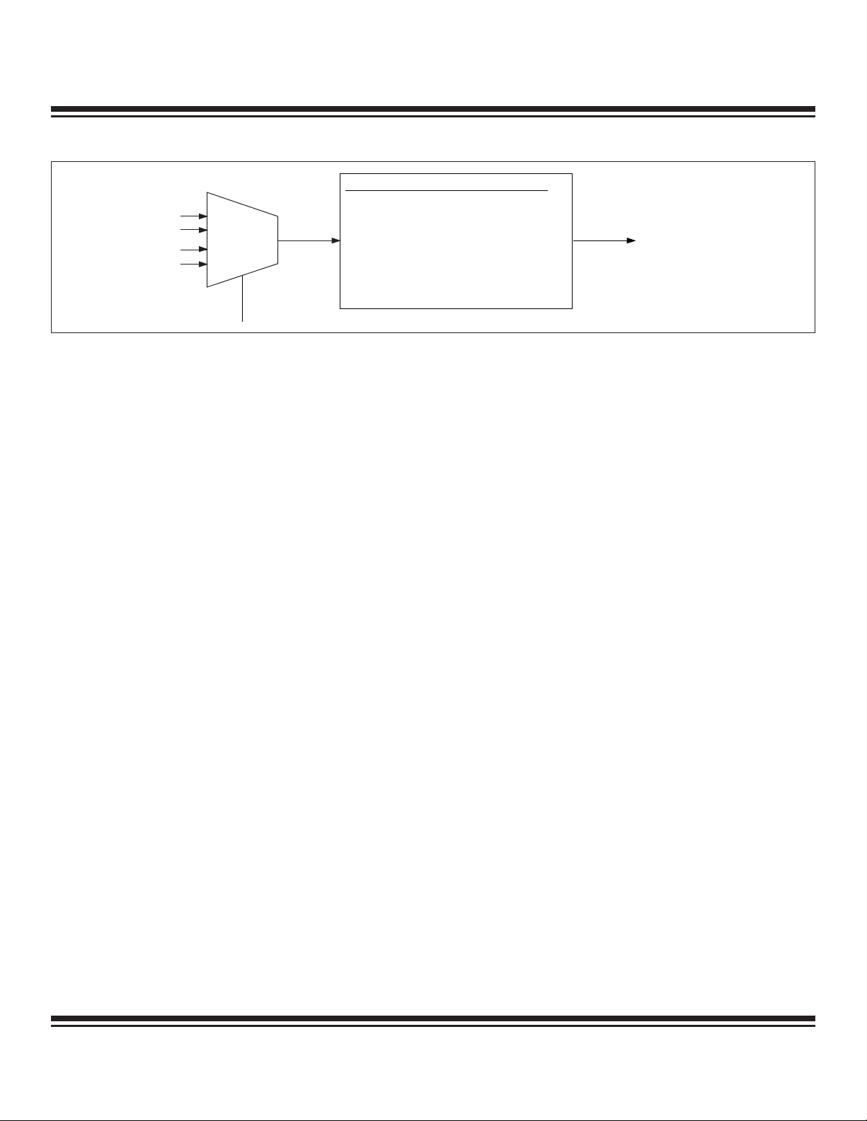
SYSTEM
CLOCK
MEMORY
CYCLE
MUX
EXECUTION
INTERNAL
EXTERNAL
NON PAGE
PAGE MODE 1 (1-CYCLE)
PAGE MODE 1 (2-CYCLE)
PAGE MODE 1 (3-CYCLE)
PAGE MODE 2
MEMORY CYCLE
SYSCLK/1
SYSCLK/4
SYSCLK/1
SYSCLK/2
SYSCLK/4
SYSCLK/2 (PROG)
SYSCLK/4 (DATA)
00
01, 10
11
Ultra-High-Speed Flash
Microcontroller User’s Guide
Figure 5-4. Instruction Memory Cycle Determination
Instruction Timing
The ultra-high-speed microcontroller executes the industry standard 8051 instruction set. Each instruction requires a minimum of one
memory cycle of execution time, and may require as many as ten memory cycles (DIV AB only). The number of memory cycles required
to execute any given 8051 instruction is documented at the end of this section and can be found in Section 14 (Instruction Set Details).
A memory cycle is the basic timing unit for the ultra-high-speed microcontroller. If internal program code is being executed, a memory cycle always consists of one system clock. If external program code is being executed, a memory cycle is then composed of 1, 2,
or 4 system clocks, as defined by the external bus configuration (non page mode, page mode 1, or page mode 2).
Calculating the number of external crystal or oscillator clock periods (t
user has configured the system clock as a function of the external clock. The system clock control function was covered earlier in the
section. As an example, if the crystal multiplier is used to generate a system clock frequency four times the frequency of the external
clock source, a nonpaged mode external memory cycle would consist of one external clock.
All instructions are coded within an 8-bit field called an op code. This single byte must be fetched from program memory. The CPU
decodes the op code to determine what action the microcontroller must take or whether additional information is needed from memory. If no other memory is needed, then only 1 byte was required. Thus, the instruction is called a 1-byte instruction. In some cases,
more data is needed. These are 2- or 3-byte instructions.
) per memory cycle additionally depends upon how the
CLCL
Single-Byte Instructions
A single-byte instruction can require anywhere between one and ten memory cycles to execute. When the execution cycle count
exceeds the byte count, the program counter must stall until instruction execution is completed. All MOVX data memory access instructions have a single-byte op code, but require more memory cycles so that data may be accessed. The MOVX instruction timing is covered in Section 6 (Memory Access). Following are examples of single byte instructions, each requiring a different number of execution
cycles:
OPCODE NO. OF CYCLES
RRC A 13h 1
DA A D4h 2
RET 22h 3
MUL AB A4h 9
DIV AB 84h 10
Maxim Integrated
5-5
Page 53

Ultra-High-Speed Flash
Microcontroller User’s Guide
2-Byte Instructions
All 2-byte instructions require a minimum of two cycles, since fetching each byte requires a separate memory access. The first byte is
the instruction op code that is decoded by the CPU. The second byte is normally an operand, or it can specify the location of the
operand. For example, “ADD A, direct” is a 2-byte, two-cycle instruction where the second byte specifies the direct address location
of the operand. Due to internal access restrictions, certain direct addressing instructions require one extra memory cycle when operating on the PSW, SP, DPS, IE, EIE, IP0, IP1, EIP0, or EIP1 register. Following are examples of these and other 2-byte instructions:
OPCODE OPERAND/LOCATION NO. OF CYCLES
ADD A, direct 25h <addr7-0> 2
ADD A, #data 24h <data7-0> 2
SJMP rel 80h <addr7-0> 3
ANL direct, A 52h <addr7-0> 2 or 3
ORL direct, A 42h <addr7-0> 2 or 3
DJNZ Rn, direct D8h-DFh <addr7-0> 4
3-Byte Instructions
Three-byte instructions require a minimum of three cycles since each byte fetch requires one memory cycle. The first byte, the opcode,
instructs the CPU on how to handle the next two bytes. Most 3-byte instructions involve comparison or branching, but not all. Just like
the 2-byte instructions, certain 3-byte instructions may require 1 extra memory cycle when operating on the PSW, SP, DPS, IE, EIE, IP0,
IP1, EIP0, or EIP1 register. Following are examples of 3-byte instructions.
OPCODE OPERAND(s)/LOCATION(s) NO. Of CYCLES
LJMP addr16 02h <addr15-8><addr7-0> 3
MOV dptr, #data16 90h <data15-8><data7-0> 3
MOV direct, direct 85h <addr7-0><addr7-0> 3 or 4
JBC bit, rel 10h <addr7-0><addr7-0> 4 or 5
DJNZ direct, rel D5h <addr7-0><addr7-0> 5
Maxim Integrated
5-6
Page 54

SYSCLK
ALE
PSEN
PORT 2
PORT 0
LSBLSB LSB
INC DPL
LSB LSB058205 86 E0 E0
MSB ADDRESS
INC DPS
SYSCLK
ALE
PSEN
PORT 2
PORT 0
MSB ADDRESS
LSB LSB
DA A RRC A
LSB LSBD4 13 13
MSB ADDRESS
Ultra-High-Speed Flash
Microcontroller User’s Guide
Nonpage Mode External Timing
The ultra-high-speed flash microcontroller defaults to a nonpage mode external memory interface. The nonpage mode bus structure
requires four system clock cycles per memory cycle. In the nonpage mode, the ALE signal latches the address LSB on each program
fetch. When the cycle count of an instruction exceeds the byte count, “dummy” fetches are performed each cycle until instruction execution is complete. Figures 5-5 to 5-8 demonstrate the basic timing for nonpage mode instruction execution.
Figure 5-5 shows the execution of the DA A instruction (1 byte, two cycles) followed by execution of the RRC A (1 byte, one cycle)
instruction. When a code fetch is made from a different 256-byte page, the new address MSB is presented on port 2.
Figure 5-6 shows the execution of the INC direct instruction (2 bytes) for the cases where an extra memory cycle is not (INC DPL) and
is (INC DPS) required.
Figure 5-5. Nonpage Mode: DA A – RRC A
Figure 5-6. Nonpage Mode: INC Direct (Two Cycles) – INC Direct (Three Cycles)
5-7
Maxim Integrated
Page 55

Ultra-High-Speed Flash
SYSCLK
ALE
PSEN
PORT 2
PORT 0
LSBLSB LSB
RET
LSB LSB2200
NOP
MSB ADDRESS MSB ADDRESS
SYSCLK
ALE
PSEN
PORT 2
PORT 0
MSB ADDRESS
LSBLSB 71 LSB
ACALL NOP
LSB3300
MSB ADDRESS
Microcontroller User’s Guide
Figure 5-7 illustrates an ACALL instruction (2 bytes, two cycles) with a destination address residing on a different 256-byte page. This
is indicated only by the MSB address change on port 2. The memory cycle duration remains constant.
Figure 5-8 shows execution of the RET instruction (1 byte, three cycles). Because the cycle count of the RET instruction exceeds the
byte count, two stall cycles (“dummy” fetches) are inserted to allow execution to complete. In this example, the return address and the
RET instruction are on different 256-byte pages (signified by the MSB address change on port 2).
Figure 5-7. Nonpage Mode: ACALL – NOP
Figure 5-8. Nonpage Mode: RET – NOP
Maxim Integrated
5-8
Page 56

MISS
STALL
SYSCLK
ALE
PSEN
PORT 2
PORT 0
DA A
D4 1313
RRC A
HIT HITHIT
LSB ADDRESS LSB ADDRESS LSB ADDRESS LSB ADDRESS
MSB ADDRESS
SYSCLK
ALE
PSEN
PORT 2
PORT 0
MSB ADDRESS
DA A RRC A
D4 13 13
LSB ADDRESS LSB ADDRESSLSB ADDRESS
MISS HIT HITSTALL
Ultra-High-Speed Flash
Microcontroller User’s Guide
Page Mode 1 External Timing—Pages 1:0 = 10b (Four Cycles)
The page mode 1 external bus structure multiplexes port 2 to provide the address MSB and LSB. Data transactions occur exclusively on port 0. ALE is used to latch the address MSB only when needed, and PSEN serves as the enable for external program memory.
Page mode 1 must be initiated by internal code memory. To invoke 4-cycle page mode 1 operation, the PAGES1:0 bits must be set to
10b, followed by the setting of the PAGEE bit. In the four-cycle page mode 1 configuration, a page-hit memory cycle is four system
clocks in length, while the page-miss memory cycle requires eight system clocks.
Figure 5-9 shows the fetch of the DA A instruction (1 byte, two cycles) during a page-miss memory cycle as would occur when a page
boundary is crossed. Like nonpage mode operation, a “dummy” or stall cycle must then be inserted for the single-byte DA A instruction, since it requires two cycles of execution time. After stalling for one cycle, the real fetch of the RRC A instruction takes place.
Figure 5-10 illustrates the fetch of the DA A instruction as the last byte of a 256-byte page. In this case, the stall cycle needed in executing the DA A instruction coincides with a page-miss memory cycle instead of a page hit (as in Figure 5-9).
Figure 5-9. Four-Cycle Page Mode 1: (Page Miss) – DA A – RRC A
Figure 5-10. Nonpage Mode: DA A – (Page Miss) – RRC A
5-9
Maxim Integrated
Page 57

Ultra-High-Speed Flash
HIT
SYSCLK
ALE
PSEN
PORT 2
PORT 0
ACALL
71
MISS HITHIT
LSB ADDRESS MSB ADDRESS LSB ADDRESS LSB ADDRESS
LSB ADDRESS
33
SYSCLK
ALE
PSEN
PORT 2
PORT 0
MSB ADDRESS
INC DPL INC DPS
05
8205 86 E0 E0
LSB ADDRESSLSB ADDRESSLSB ADDRESS
HIT HIT HIT
STALL
HIT
Microcontroller User’s Guide
Page Mode 1 External Timing—Pages 1:0 = 10b (Four Cycles) (continued)
Figure 5-11 shows execution of the INC direct instruction (2 byte, two or three cycles) for the cases where an extra memory cycle is
not (INC DPL) and is (INC DPS) required.
Figure 5-12 illustrates execution of the ACALL instruction whose destination address is on a different 256-byte page. Therefore, the
second execution cycle of the ACALL instruction is a page-miss memory cycle that requires an ALE signal toggle to be used in order
to latch a new address MSB.
Figure 5-11. Four-Cycle Page Mode 1: INC Direct (Two Cycles) – INC Direct (Three Cycles)
Figure 5-12. Four-Cycle Page Mode: ACALL – (Page Miss)
Maxim Integrated
5-10
Page 58

STALL
STALL
SYSCLK
ALE
PSEN
PORT 2
PORT 0
ACALL
22
MISSHIT
LSB ADDRESS LSB ADDRESSMSB ADDRESSLSB ADDRESS
SYSCLK
ALE
PSEN
PORT 2
PORT 0
22
HIT HIT HIT
STALL STALL
RET
LSB ADDRESS LSB ADDRESSLSB ADDRESSLSB ADDRESS
Ultra-High-Speed Flash
Microcontroller User’s Guide
Page Mode 1 External Timing—Pages 1:0 = 10b (Four Cycles) (continued)
Figure 5-13 and Figure 5-14 demonstrate the execution of the RET (1-byte, three cycles) instruction. In Figure 5-13, the return address
resides on the same 256-byte page as that of the executed RET instruction. Two stall cycles are inserted followed by a page-hit memory cycle. In Figure 5-14, the return address is on a different 256-byte page from where the RET instruction was executed. In this case,
two stall cycles are inserted, followed by a page-miss memory cycle.
Figure 5-13. Four-Cycle Page Mode 1: RET
Figure 5-14. Four-Cycle Page Mode 1: RET – (Page Miss)
5-11
Maxim Integrated
Page 59

Ultra-High-Speed Flash
SYSCLK
ALE
PSEN
PORT 2
PORT 0
02 50 00
MISS HIT MISS
LJMP ADDR16
HIT HIT HIT
LSBMSB LSB LSB LSB LSBMSB LSB
SYSCLK
ALE
PSEN
PORT 2
PORT 0
C3 13 C6
MISS HIT STALL STALL
XCH A, @R0
HIT HIT HIT
CLR C RRC A
LSBMSB LSB LSB LSBLSB ADDRESS
Microcontroller User’s Guide
Page Mode 1 External Timing—Pages 1:0 = 01b (Two Cycles)
The page mode 1 external bus structure multiplexes port 2 to provide the address MSB and LSB. Data transactions occur exclusively on port 0. ALE is used to latch the Address MSB only when needed, and PSEN serves as the enable for external program memory.
To invoke two-cycle page mode 1 operation, the PAGES1:0 bits must be set to 01b, followed by the setting of the PAGEE bit. In the
two-cycle page mode 1 configuration, a page-hit memory cycle is two system clocks in length, while the page-miss memory cycle
requires four system clocks.
Figure 5-15 shows the fetch of the CLR C instruction (1 byte, one cycle) during a page-miss memory cycle, followed by the fetch of
the RRC A instruction (1 byte, one cycle) during a page-hit memory cycle. Since the next instruction, XCH A, @R0 (1 byte, three cycles),
requires three memory cycles to execute, two stall cycles must be inserted for it to complete prior to the next instruction being read.
Figure 5-16 illustrates the LJMP (3 bytes, three cycles) instruction, whose destination address is on a different 256-byte page than the
LJMP instruction, thus resulting in a page-miss memory cycle.
Figure 5-15. Two-Cycle Page Mode 1: (Page Miss) – CLR C – RRC A – XCH A, @R0
Figure 5-16. Two-Cycle Page Mode 1: (Page Miss) – LJMP ADDR16 – (Page Miss)
Maxim Integrated
5-12
Page 60

SYSCLK
ALE
PSEN
PORT 2
PORT 0
MISS HIT HIT HIT HIT HIT HIT HIT HIT HIT HITHIT
00
45
A89045
HIT HIT
STALL
NOP
LSB
MUL AB
ORL, P1, A
SYSCLK
ALE
PSEN
PORT 2
PORT 0
MISS HIT HIT HITHIT
00D4A413C3
HIT STALLSTALLS
CLR C RRC A NOP
LSB ADDRESS
DA AMUL AB
Ultra-High-Speed Flash
Microcontroller User’s Guide
Page Mode 1 External Timing—Pages 1:0 = 00b (One Cycle)
The page mode 1 external bus structure multiplexes port 2 to provide the address MSB and LSB. Data transactions occur exclusively on port 0. ALE is used to latch the address MSB only when needed, and PSEN serves as the enable for external program memory.
Note that the one-cycle configuration differs slightly from the two-cycle and four-cycle configurations of the page mode 1 bus structure
in that PSEN does not toggle for consecutive page hits, but stays in the active-low state. To invoke one-cycle page mode 1 operation,
the PAGES 1:0 bits must be set to 00b, followed by the setting of the PAGEE bit. In the 1-cycle Page Mode 1 configuration, a page-hit
memory cycle is one system clock in length, while the page-miss memory cycle requires two system clocks.
In Figure 5-17, the CLR C (1 byte, one cycle) instruction fetch occurs during a page-miss memory cycle, followed by the RRC A instruction (1 byte, 1 cycle) instruction fetch during a page-hit memory cycle. The MUL AB (1 byte, nine cycles) instruction, which occurs
next, requires that the program counter be stalled for eight additional memory cycles so that execution can complete. In a similar fashion, the DA A (1 byte, two cycles) instruction, which follows the multiply, requires that one stall be inserted.
Figure 5-18 illustrates the memory cycle dependence of some direct instructions on the SFR addressed. The ORL direct, A is shown
for cases where P1 and IE are being addressed.
Figure 5-17. One-Cycle Page Mode 1: (Page Miss) – CLR C – MUL AB – DA A – NOP
Figure 5-18. One-Cycle Page Mode 1: (Page Miss) – ORL Direct, A (Two Cycles) – ORL, A (Three Cycles) – NOP
5-13
Maxim Integrated
Page 61

Ultra-High-Speed Flash
SYSCLK
ALE
PSEN
PORT2
P
RT0
10
D1 1D
HITHITM
ISS
J
BC PSW.1, $+20h
LSB
s
tall
H
IT
HITH
IT
s
tall
s
tall
22 75 90 55
M
ISS
HITH
IT
H
IT
M
OV P1,#55h
s
tall
R
ET
R
ET
SYSCLK
ALE
PSEN
PORT2
PORT0
10
D1 1D
HITH
IT
M
ISS
J
BC PSW.1, $+20h
LSB
22
s
tall
H
IT
HITHITs
tallstall
LSB
75 90
55
H
IT
HITH
IT
H
IT
M
OV P1,#55h
M
ISS
Microcontroller User’s Guide
Page Mode 1 External Timing—Pages 1:0 = 00b (One Cycle) (continued)
Figure 5-19 illustrates the JBC bit, rel (3 bytes, four cycles) instruction for the case where the tested bit is clear and the jump is not
taken. Note that one stall cycle must be inserted since the cycle count exceeds the byte count by one. The RET (1 byte, three cycles)
instruction that follows requires insertion of two stall cycles. In this example, the return address is on a different 256-byte page than the
RET instruction, thus resulting in a page-miss memory cycle. The MOV direct, #data (3 bytes, three cycles) executed next provides an
example of an instruction not requiring any stall cycles.
Figure 5-20 shows the same JBC bit, rel instruction for the case where the tested bit is set and the jump is taken. Since the bit must
be cleared and involves one of the special registers (PSW, SP, DPS, IE, EIE, IP0, IP1, EIP0, EIP1), a fifth memory cycle is required. For
this example, the jump taken by the JBC instruction crosses a 256-byte page boundary, while the RET instruction stays on the same
page.
Figure 5-19. One-Cycle Page Mode 1: (Page Miss) – JBC Bit, Rel (Four Cycles)) – RET – (Page Miss)– MOV Direct, Data
Figure 5-20. One-Cycle Page Mode 1: (Page Miss) – JBC Bit, Rel (Five Cycles) – (Page Miss) – RET – MOV Direct, Data
Maxim Integrated
5-14
Page 62

SYSCLK
ALE
PSEN
PORT2
PORT0
MSB
LSB LSB LSB
02 50 00
M
ISS
H
IT
HIT
LSB
M
ISS
LSB
HIT
L
JMP addr16
LSB
HIT
MSB
SYSCLK
ALE
PSEN
PORT2
PORT0
MSB
C3 13 C6
LSB LSB LSB
M
ISS
H
IT
HIT
CLR C
R
RC A
LSB Address
H
IT
LSB
HIT
X
CH A, @R0
s
tall
s
tall
Ultra-High-Speed Flash
Microcontroller User’s Guide
Page Mode 2 External Timing—Pages 1:0 = 11b
The page mode 2 external bus structure multiplexes port 2 between address MSB and data. The address LSB is provided exclusively on port 0. ALE is used to latch the address MSB only when needed, and PSEN serves as the enable for external program memory.
To invoke page mode 2 operation, the PAGES 1:0 bits must be set to 11b, followed by the setting of the PAGEE bit. In the page mode
2 configuration, a page-hit program memory cycle is two system clocks in length, while the page-miss program memory cycle requires
four system clocks. All data memory cycles are four system clocks in length.
Figure 5-21 shows the fetch of the CLR C instruction (1 byte, 1 cycle) during a page-miss memory cycle, followed by the fetch of the RRC
A instruction (1 byte, one cycle) during a page-hit memory cycle. The next instruction, XCH A, @R0 (1 byte, three cycles), requires three
memory cycles to execute, so two stall cycles must be inserted for it to complete prior to the next instruction being read.
Figure 5-22 illustrates the LJMP (3 bytes, three cycles) instruction, whose destination address is on a different 256-byte page than the
LJMP instruction, thus resulting in a page-miss memory cycle.
Figure 5-21. Page Mode 2: (Page Miss) – CLR C – RRC A – XCH A, @R0
Figure 5-22. Page Mode 2: (Page Miss) – LJMP Addr16 – (Page Miss)
5-15
Maxim Integrated
Page 63

Ultra-High-Speed Flash
INSTRUC TION HEX CODE
UHSM C LOC K
CYCLES
UHSM TI ME @
25MHz
8051 CLOCK
CYCLES
8051 TIME @
25MHz
UHSM vs. 8051
SPEED
ADVAN T AGE
ADD A, Rn 28..2F 1 40 ns 12 480 ns 12
ADD A, direct 25 2 80 ns 12 480 ns 6
ADD A, @Ri 26..27 2 80 ns 12 480 ns 6
ADD A, #data 24 2 80 ns 12 480 ns 6
ADDC A, Rn 38..3F 1 40 ns 12 480 ns 12
ADDC A, direct 35 2 80 ns 12 480 ns 6
ADDC A, @Ri 36..37 2 80 ns 12 480 ns 6
ADDC A, #data 34 2 80 ns 12 480 ns 6
SUBB A, Rn 98..9F 1 40 ns 12 480 ns 12
SUBB A, direct 95 2 80 ns 12 480 ns 6
SUBB A, @Ri 96..97 2 80 ns 12 480 ns 6
SUBB A, #data 94 2 80 ns 12 480 ns 6
INC A 04 1 40 ns 12 480 ns 12
INC Rn 08..0F 1 40 ns 12 480 ns 12
INC direct 05 2 80 ns 12 480 ns 6
INC @Ri 06..07 2 80 ns 12 480 ns 6
INC DPTR A3 1 40 ns 24 960 ns 24
DEC A 14 1 40 ns 12 480 ns 12
DEC Rn 18..1F 1 40 ns 12 480 ns 12
Microcontroller User’s Guide
Comparison to the 8051
The original 8051 needed 12 clocks per machine cycle and most instructions executed in either one or two machine cycles. Thus,
except for the MUL and DIV instructions, the 8051 used either 12 or 24 clocks for each instruction. Furthermore, each machine cycle
in the 8051 used two memory fetches. In many cases the second fetch was a dummy, and the extra clock cycles were wasted.
The ultra-high-speed microcontroller uses one clock per memory (or machine) cycle. Where there were primarily one- and two-cycle
instructions before, an instruction on the ultra-high-speed microcontroller may take between one and ten cycles. The divide instruction,
for example, requires 10 cycles. Note however, that the 10 cycles needed for the DIV AB instruction can be executed at one clock per
cycle (10 x 1 = 10 total clock cycles). The instruction is executed 4.8 times faster than the original 8051 architecture which required
four cycles at a rate of 12 clocks per cycle (4 x 12 = 48 total clock cycles). Each instruction is at least four times faster, with the highest throughput improvement being 24 times that of the original 8051 architecture.
Table 5-1 shows each instruction, the number of clocks used in the ultra-high-speed microcontroller, and the number used in the 8051 for
comparison. The factor by which the ultra-high-speed microcontroller improves on the 8051 is shown as the speed advantage. A speed
advantage of 12 means that the ultra-high-speed microcontroller performs the same instruction 12 times faster than the original 8051.
Table 5-2 provides a summary by instruction type. Note that many of the instructions provide multiple op codes. As an example, the
ADD A, Rn instruction can act on one of eight working registers. There are eight op codes for this instruction because it can be used
on eight independent locations. Table 5-2 shows totals for both number of instructions and number of op codes. Averages are provided in the tables. However, the real speed improvement seen in any system depends on the instruction mix.
Table 5-1. Instruction Timing Comparison
Ultra-high-speed microcontroller is abbreviated as UHSM.
Maxim Integrated
5-16
Page 64

INSTRUCTION HEX CODE
UHSM CLOCK
CYCLES
UHSM TIME @
25MHz
8051 CLOCK
CYCLES
8051 TIME @
25MHz
UHSM vs. 8051
SPEED
ADVANTAGE
DEC direct 15 2 80 ns 12 480 ns 6
DEC @Ri 16..17 2 80 ns 12 480 ns 6
MUL AB A4 9 360 ns 48 960 ns 5.33
DIV AB 84 10 400 ns 48 960 ns 4.80
DA A D4 2 80 ns 12 480 ns 6
ANL A, Rn 58..5F 1 40 ns 12 480 ns 12
ANL A, direct 55 2 80 ns 12 480 ns 6
ANL A, @Ri 56..57 2 80 ns 12 480 ns 6
ANL A, #data 54 2 80 ns 12 480 ns 6
ANL direct, A 52 2 80 ns 12 480 ns 6
ANL direct, #data 53 3 120 ns 24 960 ns 8
ORL A, Rn 48..4F 1 40 ns 12 480 ns 12
ORL A, direct 45 2 80 ns 12 480 ns 6
ORL A, @Ri 46..47 2 80 ns 12 480 ns 6
ORL A, #data 44 2 80 ns 12 480 ns 6
ORL direct, A 42 2 80 ns 12 480 ns 6
ORL direct, #data 43 3 120 ns 24 960 ns 8
XRL A, Rn 68..6F 1 40 ns 12 480 ns 12
XRL A, direct 65 2 80 ns 12 480 ns 6
XRL A, @Ri 66..67 2 80 ns 12 480ns 6
XRL A, #data 64 2 80 ns 12 480 ns 6
XRL direct, A 62 2 80 ns 12 480 ns 6
XRL direct, #data 63 3 120 ns 24 960 ns 8
CLR A E4 1 40 ns 12 480 ns 12
CPL A F4 1 40 ns 12 480 ns 12
RL A 23 1 40 ns 12 480 ns 12
RLC A 33 1 40 ns 12 480 ns 12
RR A 03 1 40 ns 12 480 ns 12
RRC A 13 1 40 ns 12 480 ns 12
SWAP A C4 1 40 ns 12 480 ns 12
MOV A, Rn E8..EF 1 40 ns 12 480 ns 12
MOV A, direct E5 2 80 ns 12 480 ns 6
MOV A, @Ri E6..E7 2 80 ns 12 480 ns 6
MOV A, #data 74 2 80 ns 12 480 ns 6
MOV Rn, A F8..FF 1 40 ns 12 480 ns 12
Ultra-High-Speed Flash
Microcontroller User’s Guide
Table 5-1. Instruction Timing Comparison (continued)
5-17
Maxim Integrated
Page 65

Microcontroller User’s Guide
INSTRUC TION HEX CODE
UHSM C LOC K
CYCLES
UHSM TI ME @
25MHz
8051 CLOCK
CYCLES
8051 TIME @
25MHz
UHSM vs. 8051
SPEED
ADVAN T AGE
MOV Rn, d i rect A8..AF 2 80 ns 24 960 ns 12
MOV Rn, #data 78..7F 2 80 ns 12 480 ns 6
MOV direct, A F5 2 80 ns 12 480 ns 6
MOV direct, Rn 88..8F 2 80 ns 24 960 ns 12
MOV direct, direct 85 3 120 ns 24 960 ns 8
MOV direct, @Ri 86..87 2 80 ns 24 960 ns 12
MOV direct, #data 75 3 120 ns 24 960 ns 8
MOV @Ri, A F6..F7 1 40 ns 12 480 ns 12
MOV @Ri, direct A6..A7 2 80 ns 24 960 ns 12
MOV @Ri, #data 76..77 2 80 ns 12 480 ns 6
MOV DPTR, #data 16 90 3 120 ns 24 960 ns 8
MOVC A, @A+DPTR 93 3 120 ns 24 960 ns 8
MOVC A, @A+PC 83 3 120 ns 24 960 ns 8
MOVX A, @Ri E2..E3 2 80 ns 24 960 ns 12
MOVX A, @DPTR E0 2 80 ns 24 960 ns 12
MOVX @Ri, A F2..F3 2 80 ns 24 960 ns 12
MOVX @DPTR, A F0 2 80 ns 24 960 ns 12
PUS H d i rect C0 2 80 ns 24 960 ns 12
POP direct D0 2 80 ns 24 960 ns 12
XCH A, Rn C 8..CF 2 80 ns 12 480 ns 6
XCH A, direct C 5 3 120 ns 12 480 ns 4
XCH A, @Ri C6..C7 3 120 ns 12 480 ns 4
XCH D A, @Ri D6..D7 3 120 ns 12 480 ns 4
CLR C C3 1 40 ns 12 480 ns 12
CLR bit C2 2 80 ns 12 480 ns 6
SETB C D3 1 40 ns 12 480 ns 12
SETB bit D2 2 80 ns 12 480 ns 6
CPL C B3 1 40 ns 12 480 ns 12
CPL bit B2 2 80 ns 12 480 ns 6
ANL C, bit 82 2 80 ns 24 960 ns 12
ANL C, B0 2 80 ns 24 960 ns 12
ORL C, bit 72 2 80 ns 24 960 ns 12
ORL C, A0 2 80 ns 24 960 ns 12
MOV C, bit A2 2 80 ns 12 480 ns 6
MOV bit, C 92 2 80 ns 24 960 ns 12
Table 5-1. Instruction Timing Comparison (continued)
Ultra-High-Speed Flash
Maxim Integrated
5-18
Page 66

INSTRUCTION HEX CODE
UHSM CLOCK
CYCLES
UHSM TIME @
25MHz
8051 CLOCK
CYCLES
8051 TIME @
25MHz
UHSM vs. 8051
SPEED
ADVANTAGE
ACALL addr 11 Hex code
Hex codes = 11, 31, 51, 71,
91, B1, D1, or F1
Byte 1 2 80 ns 24 960 ns 12
LCALL addr 16 12 3 120 ns 24 960 ns 8
RET 22 3 120 ns 24 960 ns 8
RETI 32 3 120 ns 24 960 ns 8
AJMP addr 11 Hex code
Hex code = 01, 21, 41, 61,
81, A1, C1, or E1
Byte 1 2 80 ns 24 960 ns 12
LJMP addr 16 02 3 120 ns 24 960 ns 8
JMP @A+DPTR 73 3 120 ns 24 960 ns 8
SJMP rel 80 3 120 ns 24 960 ns 8
JZ rel 60 3 120 ns 24 960ns 8
JNZ rel 70 3 120 ns 24 960 ns 8
JC rel 40 3 120 ns 24 960 ns 8
JNC rel 50 3 120 ns 24 960 ns 8
JB bit, rel 20 4 160 ns 24 960 ns 6
JNB bit, rel 30 4 160 ns 24 960 ns 6
JBC bit, rel 10 4 160 ns 24 960 ns 6
CJNE A, direct, rel B5 5 200 ns 24 960 ns 4.8
CJNE A, #data, rel B4 4 160 ns 24 960 ns 6
CJNE Rn, #data, rel B8..BF 4 160 ns 24 960 ns 6
CJNE @Ri, #data, rel B6..B7 5 200 ns 24 960 ns 4.8
DJNZ Rn, rel D8..DF 4 160 ns 24 960 ns 6
DJNZ direct, rel D5 5 200 ns 24 960 ns 4.8
NOP 00 1 40 ns 12 480 ns 12
Ultra-High-Speed Flash
Microcontroller User’s Guide
Table 5-1. Instruction Timing Comparison (continued)
5-19
Maxim Integrated
Page 67

Table 5-2. Instruction Speed Summary
INSTRUC TION CATEGORY
SPEED
ADVAN T AGE
QUAN TITY
4.0 2
4.8 1
5.3 1
6.0 12
8.0 5
12.0 27
Total instructions: 1 byte
24.0 1
4.0 1
6.0 27
8.0 5
Total instructions: 2 byte
12.0 13
4.8 3
6.0 5
Total instructions: 3 byte
8.0 8
Average across all instructions 8.5 111
OPCODE CATEGORY
SPEED
ADVAN T AGE
QUAN TITY
4.0 4
4.8 1
5.3 1
6.0 35
8.0 5
12.0 93
Total opcodes: 1 byte
24.0 1
4.0 1
6.0 42
8.0 5
Total opcodes: 2 byte
12.0 43
4.8 4
6.0 12
Total opcodes: 3 byte
8.0 8
Average across all opcodes 9.4 255
Ultra-High-Speed Flash
Microcontroller User’s Guide
Maxim Integrated
5-20
Page 68

Ultra-High-Speed Flash
Microcontroller User’s Guide
SECTION 6: MEMORY ACCESS
This section contains the following information:
Internal Flash Memory . . . . . . . . . . . . . . . . . . . . . . . . . . . . . . . . . . . . . . . . . . . . . . . . . . . . . . . . . .6-3
ROMSize Feature . . . . . . . . . . . . . . . . . . . . . . . . . . . . . . . . . . . . . . . . . . . . . . . . . . . . . . . . . . . . . .6-3
Flash Security Block/Lock Bits . . . . . . . . . . . . . . . . . . . . . . . . . . . . . . . . . . . . . . . . . . . . . . . . . . . .6-4
Option Control Register Byte . . . . . . . . . . . . . . . . . . . . . . . . . . . . . . . . . . . . . . . . . . . . . . . . . . . . .6-5
Internal SRAM Memory . . . . . . . . . . . . . . . . . . . . . . . . . . . . . . . . . . . . . . . . . . . . . . . . . . . . . . . . . .6-6
Program Memory Interface—Nonpage Mode . . . . . . . . . . . . . . . . . . . . . . . . . . . . . . . . . . . . . . . .6-6
Program Memory Interface—Page Modes . . . . . . . . . . . . . . . . . . . . . . . . . . . . . . . . . . . . . . . . . .6-8
Page Mode 1 Bus Structure . . . . . . . . . . . . . . . . . . . . . . . . . . . . . . . . . . . . . . . . . . . . . . . . . .6-9
Page Mode 2 Bus Structure . . . . . . . . . . . . . . . . . . . . . . . . . . . . . . . . . . . . . . . . . . . . . . . . . .6-11
Data Memory Interface . . . . . . . . . . . . . . . . . . . . . . . . . . . . . . . . . . . . . . . . . . . . . . . . . . . . . . . . . .6-12
External Data Memory Interface—Nonpage Mode . . . . . . . . . . . . . . . . . . . . . . . . . . . . . . . .6-12
External Data Memory Interface—Page Modes . . . . . . . . . . . . . . . . . . . . . . . . . . . . . . . . . .6-13
Page Mode 1 Data Memory Timing–PAGES 1:0 = 10b (Four Cycles) . . . . . . . . . . . . . . . . . . . . .6-17
Page Mode 1 Data Memory Timing–Pages 1:0 = 01b (Two Cycles) . . . . . . . . . . . . . . . . . . . . . . .6-18
Page Mode 1 Data Memory Timing–Pages 1:0 = 00b (One Cycle) . . . . . . . . . . . . . . . . . . . . . . .6-20
Page Mode 2 Data Memory Timing–Pages 1:0 = 11b (Four Cycles) . . . . . . . . . . . . . . . . . . . . . .6-22
Data Memory Access . . . . . . . . . . . . . . . . . . . . . . . . . . . . . . . . . . . . . . . . . . . . . . . . . . . . . . . . . . .6-22
6-1
Maxim Integrated
Page 69

Ultra-High-Speed Flash
Microcontroller User’s Guide
LIST OF FIGURES
Figure 6-1. Memory Map for the DS89C420/430 . . . . . . . . . . . . . . . . . . . . . . . . . . . . . . . . . . . . . .6-5
Figure 6-2. Program Memory Interconnect (Nonpage Mode) . . . . . . . . . . . . . . . . . . . . . . . . . . . .6-7
Figure 6-3. External Program Memory Access (Nonpage Mode and CD1:0 = 10b) . . . . . . . . . .6-7
Figure 6-4 Program Memory Interconnect (Page Mode 1) . . . . . . . . . . . . . . . . . . . . . . . . . . . . . .6-9
Figure 6-5. Page Mode 1 External Memory Cycle (CD1:0 = 10b) . . . . . . . . . . . . . . . . . . . . . . . .6-10
Figure 6-6. Program Memory Interconnect (Page Mode 2) . . . . . . . . . . . . . . . . . . . . . . . . . . . . . .6-11
Figure 6-7. Page Mode 2 External Code Fetch Cycle (CD1:0 = 10b) . . . . . . . . . . . . . . . . . . . . . .6-11
Figure 6-8. Data Memory Interconnect (Nonpage Mode) . . . . . . . . . . . . . . . . . . . . . . . . . . . . . . .6-13
Figure 6-9. Data Memory Interconnect (Page Mode 1) . . . . . . . . . . . . . . . . . . . . . . . . . . . . . . . . .6-15
Figure 6-10. Data Memory Interface (Page Mode 2) . . . . . . . . . . . . . . . . . . . . . . . . . . . . . . . . . . .6-15
Figure 6-11. Nonpage Mode: MOVX (Two Cycles) . . . . . . . . . . . . . . . . . . . . . . . . . . . . . . . . . . . .6-16
Figure 6-12. Nonpage Mode: MOVX (Three Cycles) . . . . . . . . . . . . . . . . . . . . . . . . . . . . . . . . . . .6-16
Figure 6-13. Four-Cycle Page Mode 1: MOVX (Two Cycles) . . . . . . . . . . . . . . . . . . . . . . . . . . . . .6-17
Figure 6-14. Four-Cycle Page Mode 1: MOVX (Three Cycles) . . . . . . . . . . . . . . . . . . . . . . . . . . .6-17
Figure 6-15. Two-Cycle Page Mode 1: MOVX (Two Cycles) . . . . . . . . . . . . . . . . . . . . . . . . . . . . .6-18
Figure 6-16. Two-Cycle Page Mode 1: MOVX (Three Cycles) . . . . . . . . . . . . . . . . . . . . . . . . . . . .6-18
Figure 6-17. Two-Cycle Page Mode 1: MOVX (Three Cycles) External Code
Execution with Page Misses . . . . . . . . . . . . . . . . . . . . . . . . . . . . . . . . . . . . . . . . . . .6-19
Figure 6-18. Two-Cycle Page Mode 1: MOVX (Three Cycles) External Code
Execution - No Page Misses . . . . . . . . . . . . . . . . . . . . . . . . . . . . . . . . . . . . . . . . . . .6-19
Figure 6-19. One-Cycle Page Mode 1: MOVX (Three Cycles)—MOVX (Three Cycles) . . . . . . . .6-20
Figure 6-20. One-Cycle Page Mode 1: MOVX (Two Cycles)—MOVX (Two Cycles) . . . . . . . . . . .6-20
Figure 6-21. One-Cycle Page Mode 1: MOVX (Two Cycles)—MOVX (Two Cycles)
External Code Execution . . . . . . . . . . . . . . . . . . . . . . . . . . . . . . . . . . . . . . . . . . . . . .6-21
Figure 6-22. One-Cycle Page Mode 1: MOVX (Nine Cycles) External Code Execution . . . . . . . .6-21
LIST OF TABLES
Table 6-1. Flash Memory Lock Bits . . . . . . . . . . . . . . . . . . . . . . . . . . . . . . . . . . . . . . . . . . . . . . . .6-4
Table 6-2. Data Memory Access Control . . . . . . . . . . . . . . . . . . . . . . . . . . . . . . . . . . . . . . . . . . . .6-6
Table 6-3. Page Mode Select . . . . . . . . . . . . . . . . . . . . . . . . . . . . . . . . . . . . . . . . . . . . . . . . . . . . .6-8
Table 6-4. Nonpage Mode Data Memory Stretch Values . . . . . . . . . . . . . . . . . . . . . . . . . . . . . . . .6-12
Table 6-5. Page Mode 1—Data Memory Stretch Values 1 Cycle (PAGES 1:0 = 00b) . . . . . . . . .6-13
Table 6-6. Page Mode 1—Data Memory Stretch Values Two Cycles (Pages 1:0 = 01b) . . . . . . .6-14
Table 6-7. Page Mode 1—Data Memory Stretch Values Four Cycles (Pages 1:0 = 10b) . . . . . . .6-14
Table 6-8. Page Mode 2—Data Memory Stretch Values (Pages 1:0 = 11b) . . . . . . . . . . . . . . . . .6-14
Table 6-9. Enhanced Data Pointer Speed Improvement . . . . . . . . . . . . . . . . . . . . . . . . . . . . . . .6-23
Maxim Integrated
6-2
Page 70

Ultra-High-Speed Flash
Microcontroller User’s Guide
SECTION 6: MEMORY ACCESS
The ultra-high-speed flash microcontroller supports the memory interface convention established for the industry standard 80C51, but
also implements two new page mode memory interfaces needed to support ultra-high-speed external operation. These external page
mode interfaces are described later in this section.
Program and data memory areas can be implemented on-chip, off-chip, or as a combination. When opting not to use the internal memory provided, or when exceeding the maximum address of on-chip program or data memory, the device performs an external memory access using the expanded memory bus on ports 0 and 2. While serving as a memory bus, port 0 and port 2 cannot function as
I/O ports. The PSEN signal is driven active low to function as a chip enable or output enable when performing external code memory
fetches. The RD and WR signals serve as enables when accessing external SRAM data memory.
Pr
ogram execution always begins at the reset vector, address 0000h. If on-chip program memory is enabled, program execution
begins at internal location 0000h; otherwise, external program memor
this location. Subsequent branches and interrupts determine how program memory fetches deviate from sequential addressing.
Internal Flash Memory
The ultra-high-speed flash microcontroller contains five physically distinct blocks of embedded flash memory. The two largest blocks
are each half of the total amount of internal program memory. A 64-byte flash security block has been incorporated to allow encryption during program memory verify operations. To further protect internal code against undesirable access, a three-level lock system
has been implemented in a separate flash memory block. This single-byte block contains three lock bits (LB1, LB2, LB3), each of which
can individually enable higher lock levels and greater code protection. The fifth flash memory block is the option control register. This
byte contains a bit to enable or disable the watchdog timer reset function (EWT = WDCON.1) on a power-on reset.
The two program memory blocks form a contiguous address range extending from 0000h through the maximum amount of on-chip
program memory. The on-chip decoded address range is controlled in hardware by the EA pin, and in software through the ROMSIZE
feature. The EA pin enables or disables the ability to access internal program memory and overrides any software configured bit settings. The logic state of the EA pin should be changed only when the microcontroller is being held in reset. The EA pin is sampled on
each exit from the reset state to determine whether program fetching should begin internally or externally. When the EA pin is low
code fetches are done externally through the expanded bus. When the EA pin is high, code fetches begin fr
ory. Code fetches exceeding the maximum address of on-chip program memory cause the device to access off-chip program memory. The maximum on-chip decoded address is selectable by softwar
y is used. Any reset causes the next program fetch to begin at
, all
om internal program mem-
e using the ROMSIZE feature.
ROMSize Feature
Using the ROMSIZE feature, software can imitate a device with less on-chip memory. The maximum memory size is dynamically variable. Thus, a portion of memory can be removed from the memory map to access off-chip memory, then be restored to access onchip memory. In fact, all of the on-chip memory can be removed from the memory map, allowing the full 64kB of external memory space
to be addressed.
The ROMSIZE feature has two primary uses. In the first instance, it allows the device to act as a bootstrap loader for a flash memory
or nonvolatile SRAM (NVSRAM). The internal program memory can contain a bootstrap loader, which can program the external memory device. Secondly, this method can be used to increase the amount of available program memory from 64kB to 80kB without bank
switching.
The maximum amount of on-chip memory is selected by configuring the ROM size select register bits RMS2, RMS1, RMS0 (ROMSIZE.2-0). The reset default condition gives access to the maximum on-chip program memory. In this configuration, only code addresses greater than the maximum amount of on-chip program memory result in external program memory accesses. The possible settings
for the ROM size select register are shown in the ROMSIZE special-function register.
6-3
Maxim Integrated
Page 71

Ultra-High-Speed Flash
LEVEL LB1 LB2 LB3 PROTECTION
1 1 1 1 No progra m lock. Encry pted verify if encryption array is prog ram med.
2 0 1 1
Prevent MOVC in external memory from reading p rog ram code in internal memory. EA is
sampled and latched on reset. Allow no further parallel or program memory Loader
programm ing.
3 X 0 1
Level 2 plus no verify operation. Also prevent MOVX in external me mory from reading internal
SRAM.
4 X X 0 Level 3 plus no external execution.
Microcontroller User’s Guide
Modification of the ROMSIZE (C2h) special function register requires using the timed access procedure and must be followed by a two
machine cycle delay, such as executing two NOP instructions, before jumping to the new address range. Interrupts must be disabled
during this operation, because a call to an interrupt vector during the changing of the memory map can cause erratic results. To select
a different internal program memory size, software must alter bits RMS2–RMS0. The procedure to reconfigure the size of on-chip memory should be done as follows:
1) Jump to a location in program memory that is unaffected by the change.
2) Disable interrupts by clearing the EA bit (IE.7).
3) Write AAh to the timed access register (TA;C7h).
4) Write 55h to the timed access register (TA;C7h).
5) Modify the ROM size select bits (RMS2-RMS0).
6) Delay 2 machine cycles (2 NOP instructions).
7) Enable interrupts by setting the EA bit (IE.7).
As noted in the first step above, ensure that changes to the ROMSIZE register do not corrupt program execution. For example, assume
that a 16kB DS89C430 is executing instructions from internal program memory near the 12kB boundary (~3000h) and the ROMSIZE
register is still configured to the default internal program space. If software reconfigures the ROMSIZE register for a maximum of 4kB
(0000h–0FFFh) internal program space (RMS2–0 = 011b), the device immediately accesses external program memory since current
program execution no longer resides within the new on-chip decoded range. This could result in code misalignment and execution of
an invalid instruction. The recommended method is to modify the ROMSIZE register from a location in memory that is internal (or external) both before and after the operation. In the above example, the instruction which modifies the ROMSIZE register should be located below the 4kB (1000h) boundary or above the maximum boundary, so that it is unaffected by the memory modification. The same
rule applies when executing from external program memory and increasing the on-chip decoded address range.
If the 0kB of internal program memory setting is selected, take extra precautions. In this case, it is necessary to duplicate the interrupt
vector table in external program memory. This is because the interrupt vector table is located in the lower 1kB of memory, and the
device automatically redirects any fetches from the interrupt vector table to external memory. Be careful when assembling or compiling the program so that all the modules are located at the correct starting address, including the interrupt vector table.
Flash Security Block/Lock Bits
The device incorporates a 64-byte encryption array, allowing the user to verify program codes while viewing the data in encrypted form.
The encryption array, often referred to as the security block, has the same electrical and timing characteristics as the on-chip program
memory. Once the encryption array is programmed to non-FFh, the data presented in the verify mode is encrypted. Each byte of data
is XNORed with a byte in the encryption array during verification. If the security block is used, program unused portions of the internal
flash program memory range with random data so that the encryption vector cannot be easily extracted.
The single byte, which contains the 3 lock bits, logically resides at byte address 40h of the security block. The 3 lock bits (LB3, LB2,
and LB1) can be accessed in bit positions 5, 4, and 3, respectively. By programming the 3 lock bits, the user may select a level of
security as specified in Table 6-1. Once a security level is selected and programmed, the setting of the lock bits remains. Only a mass
erase erases these bits and allows reprogramming the security level to a less restricted protection.
Table 6-1. Flash Memory Lock Bits
The lock bits affect the read/write accessibility in program memory loader and parallel programming modes.
Maxim Integrated
6-4
Page 72

External
Data
Memory
8kB x 8
Flash
Memory
(Program)
1kB x 8
SRAM
Data OR
prog mem
addr from
400–7FF
128 Bytes
Indirect
Addressing
Bit Addressable
Bank 3
Bank 2
Bank 1
Bank 0
00
1F
20
2F
7F
80
128 Bytes SFR
FF
0000
1FFF
2000
3FFF
INTERNAL
MEMORY
03FF
0000
FFFF
FFFF
4000
00000000
03FF
External
Program
Memory
INTERNAL
REGISTERS
8kB x 8
Flash
Memory
(Program)
SCRATCH
PAD
Note: The hatched areas shown on the internal and external
memory are disabled on power-up (Default)
Non-usable if
Internal SRAM
is activated
Ultra-High-Speed Flash
Microcontroller User’s Guide
Option Control Register Byte
User-selectable options are present that must be set before beginning software execution. The option control register uses flash bits,
rather than SFRs, and is individually erasable and programmable as a byte-wide register. Bit 3 of this register is defined as the watchdog POR default. Setting this bit to 1 disables the watchdog reset function on power-up, and clearing this bit to 0 enables the watchdog
reset function automatically. Other bits of this register are undefined and are at logic 1 when read. The value of this register can be read
at address FCh in parallel programming mode or by executing the verify option control register instruction in ROM Loader mode.
Figure 6-1. Memory Map for the DS89C420/430
6-5
Maxim Integrated
Page 73

Ultra-High-Speed Flash
DME1 DME0 DAT A MEMORY ADD RESS RANG E DATA MEMORY LOCATION
0 0 0000h–FFFFh External Data Memory (default)
X 1
0000h–03FFh
0400h–FFFFh
Internal Data Memory
External Data Memory
1 0 Reserved Reserv ed
Microcontroller User’s Guide
Internal SRAM Memory
The ultra-high-speed microcontroller incorporates an internal 1kB SRAM that is usable as data, program, or merged program/data memory. Upon a power-on reset, the internal 1kB memory is disabled and transparent to both program and data memory maps.
When used for data, the memory is addressed through MOVX commands, and is in addition to the 256 bytes of scratchpad memory.
To enable the 1kB SRAM as internal data memory, software must set the DME0 bit (PMR.0). After setting this bit, all MOVX accesses
within the first 1kB (0000h–03FFh) are directed to the internal SRAM. Any data memory accesses outside of this range are still directed to the expanded bus. One advantage of using the internal data memory is that MOVX operations automatically default to the fastest
access possible. Note that the DME0 bit is cleared after any reset, so access to the internal data memory is prohibited until this bit is
modified. The contents of the internal data memory are not affected by the changing of the data memory enable (DME0) bit.
Table 6-2 shows how the DME1, DME0 bits affect the data memory map.
Table 6-2. Data Memory Access Control
When configured as program memory, code fetches and MOVC read operations can be directed to this 1kB internal SRAM. To enable
the 1kB SRAM as internal program memory, software must set the PRAME bit (ROMSIZE.3). After setting this bit, code accesses to the
address range 0400h–07FFh are made to the internal 1kB SRAM in place of the program memory previously mapped to that address
range. For applications using only external program memory (EA = 0), the inter
The internal 1kB SRAM can serve as merged program/data memory if both the DME0 and PRAME bits have been set. This feature can
be effective for changing small pieces of frequently executed code, but be cautious when employing self-modifying code techniques.
nal 1kB SRAM cannot be enabled as program space.
Program Memory Interface—Nonpage Mode
The ultra-high-speed flash microcontroller defaults to a nonpage mode, external program memory interface. This memory interconnect
scheme is the same as is used for the high-speed microcontroller family, and is shown in Figure 6-2. This example uses the DS89C420
and one 64k x 8 memory device. The program store enable (PSEN) signal is used to provide an output enable to the memory. It can
also be used to provide a chip enable, but this generally results in less-favorable timing. The address LSB and data are multiplexed
on port 0, and the address MSB is provided on port 2. An external latch, shown in the diagram as a 74F373, is used to latch the lower
byte of the address to the memory device. The address latch enable (ALE) signal controls the timing of the latch so that the operation
is performed in the proper sequence. The signals and relative timing for a program access are shown in Figure 6-3.
When implementing a high-speed memory interface, the F series (or faster) logic should be used. HC logic has worst-case propagation delays that are too long. Specifications for all devices should be checked. More information on the nonpage mode memory interface timing can be found in Application Note 57 (DS80C320 Memory Interface Timing) and Application Note 85 (High-Speed
Microcontroller Interface Timing).
The DS89C420 provides an extremely high-speed interface to external memory. This allows for use of the slowest, and least expensive, memory device for a given crystal speed. The ultra-high-speed flash microcontroller provides very fast slew rates to allow the
maximum possible time for memor
y access. Refer to the electrical specifications for exact timing.
Maxim Integrated
6-6
Page 74

Internal Memory Cycles
C2 C3 C4 C1 C2 C3 C4
XTAL1
ALE
Port 0
Port 2
PSEN
C1
Ext Memory CycleExt Memory Cycle
MSB Add MSB Add
LSB Add Data LSB Add Data
PSEN
ALE
CK
74F373
LATCH
LSB ADDRESS
DATA BUS
MSB ADDRESS
PORT 2
(8)
(7)
64kB X 8
MEMORY
(8)
OE
CE
PORT 0
DS89C4x0
Ultra-High-Speed Flash
Microcontroller User’s Guide
Figure 6-2. Program Memory Interconnect (Nonpage Mode)
Figure 6-3 shows the timing relationship for internal and external nonpage mode code fetches when CD1:0 = 10b. Note that an external program fetch takes four system clocks, and an internal program fetch requires only one system clock.
As illustrated in that same figure, ALE is deasserted when executing an internal memory fetch. The microcontroller provides a programmable user option (ALEON bit = PMR.2) to turn on the ALE signal during internal program memory operation. The ALE signal is
automatically enabled for external code fetches, independent of the setting of this bit. PSEN is asserted only for external code fetches, and is inactive during internal execution.
Figure 6-3. External Program Memory Access (Nonpage Mode and CD1:0 = 10b)
6-7
Maxim Integrated
Page 75

Ultra-High-Speed Flash
EXTERNAL AD D RESSING CLOCKS PER MEMORY CYCLE
MODE
PAGES1:PAGES0
PAGE HIT PAGE MISS
EXTERNAL BUS STRUCTU RE
Page mode 1 (1 cycle) 00 1 2 PAGE MODE 1
Page mode 1 (2 cycle) 01 2 4 PAGE MODE 1
Page mode 1 (4 cycle) 10 4 8 PAGE MODE 1
Page mode 2 11 2* 4 PAGE MODE 2
Microcontroller User’s Guide
Program Memory Interface—Page Modes
Page mode retains the basic external circuitry requirements as the original 8051 external memory interface, but modifies the
address/data roles of P0 and P2 in order to achieve the most efficient single-cycle external operation possible. The functions of ALE
and PSEN are also altered to support page mode operation.
Page mode is enabled by setting the PAGEE (ACON.7) bit to a logic 1. Clearing the PAGEE bit disables the page mode and returns
to the traditional external bus structure of the 8051 (nonpage mode). Page mode is supported in two external bus structures. The page
mode select bits (PAGES1:0) contained in the ACON r
per basic memory cycle. The following table summarizes the four options available through the PAGES bits. The first three selections
all represent the page mode 1 external bus structure, but with different memory cycle timings. The last configuration (PAGES = 11b)
selects the page mode 2 bus structure.
Table 6-3. Page Mode Select
Note: External data memory accesses always require four clock cycles, regardless of page hit or page miss.
egister determine the external bus structure and the number of system clocks
PAGE MODE 1: P0: Primary data bus.
P2: Primary address bus, multiplexing the upper byte and lower byte of address.
PAGE MODE 2: P0: Lower address byte.
P2: Upper address byte is multiplexed with the data byte.
In addition to being accessible to the user application code, the page mode enable and select bits can also be modified while in ROM
loader mode. This allows in-system MOVX read/write access to external memory already connected according to the page mode 1 or
page mode 2 bus structure. Since all resets, including the one generated when exiting ROM loader mode, return to the nonpage mode
external bus structure, user application code must always configure the ACON register appropriately before addressing page mode
external memory. Write access to the ACON register requires using the timed access procedure.
Maxim Integrated
6-8
Page 76

PSEN
ALE
CK
74F373
LATCH
MSB ADDRESS
LSB ADDRESS
DATA BUS
PORT 0
(8)
(8)
64kB X 8
MEMORY
(8)
OE
CE
PORT 2
DS89C4x0
Ultra-High-Speed Flash
Microcontroller User’s Guide
Page Mode 1 Bus Structure
The page mode 1 external bus structure uses P2 as the primary address bus (multiplexing both the most significant byte and least significant byte of the address for each external memory cycle), and P0 is used as the primary data bus. This program memory interconnect scheme is depicted in Figure 6-4.
Figure 6-4 Program Memory Interconnect (Page Mode 1)
During external code fetches, P0 is held in a high-impedance state by the processor. Opcodes are driven by the external memory onto
P0 and latched on the rising edge of PSEN at the end of the external fetch cycle.
• A page miss occurs when the most significant byte of the subsequent address is different from the last address. The external
memory machine cycle can be 2, 4, or 8 system clocks in length for a page miss.
• A page hit occurs when the most significant byte of the subsequent address does not change from the last address. The external memory machine cycle can be 1, 2, or 4 system clocks in length for a page hit.
During a page hit, P2 drives Addr [7:0] of the 16-bit addr
es. PSEN, RD, and RD strobe accordingly for the appropriate operation on the P0 data bus. There is no ALE assertion for page hits.
During a page miss, P2 drives the Addr [15:8] of the 16-bit address and holds it for the duration of the first half of the memory cycle
to allow the external address latches to latch the new most significant address byte. ALE is asserted to strobe the external address
latches. During this operation, PSEN, RD, and WR are all held in inactive states and P0 is in a high-impedance state. The following halfmemor
y cycle is executed as a page-hit cycle and the appropriate operation takes place.
A page-miss can occur at set intervals or during external operations that require a memory access into a page of memory that has not
been accessed during the last external cycle. Generally, the first external memory access causes a page miss. The new page address
is stored internally and is used to detect a page miss for the current external memory cycle.
Note that ther
e are a few exceptions for this mode of operation when PAGES1 and PAGES2 are set to 00b:
• PSEN is asserted for both page hit and page miss for a full clock cycle.
•
The execution of external MOVX instruction causes a page miss.
• A page miss occurs when fetching the next external instruction following the execution of an external MOVX instruction.
ess while the most significant address byte is held in the external address latch-
6-9
Maxim Integrated
Page 77
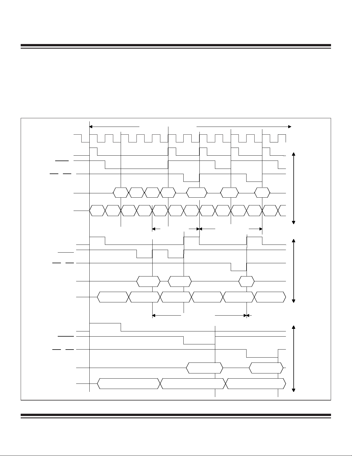
Ultra-High-Speed Flash
Internal Memory Cycles
XTAL1
ALE
Port 0
Port 2
DataData
Inst
MSB MSB MSB MSBMSB LSB LSB LSB LSB LSB LSB
InstInst
External Memory Cycles
Page MissPage HitPage Miss Data Access Data Access
PAGES=00
ALE
PSEN
MOVX
Inst
Data
Page Miss Page MissData AccessPage Hit
MSBAdd LSB Add LSB Add MSBAdd MSBAddLSB Add
PAGES=01
Port 0
Port 2
MSBAdd LSB Add LSB Add
Inst
Data
Port 2
Port 0
PSEN
ALE
Page Miss Data Access
RD / WR
RD / WR
PAGES=10
RD / WR
MOVX MOVX
LSB
PSEN
MOVX executed
MOVX executedMOVX executed
next instruction
Microcontroller User’s Guide
Figure 6-5 shows external memory cycles for the page mode 1 bus structure. The first case illustrates a back-to-back MOVX execution sequence for one-cycle page mode (PAGES 1:0 = 00b). PSEN remains active during page-hit cycles, and page misses are forced
during and after MOVX executions, independent of the most significant byte of the subsequent addresses. The second case illustrates
a MOVX execution sequence for two-cycle page mode (PAGES 1:0 = 01b). PSEN is active for a full clock cycle in code fetches. Note
that the page misses in this sequence are caused by changing of the most significant byte of the data address. The thir
trates a MOVX execution sequence for four-cycle page mode (PAGES 1:0 = 10b). There is no page-miss in this execution cycle, as the
most significant byte of the data address is assumed to match the last program address.
d case illus-
Figure 6-5. Page Mode 1 External Memory Cycle (CD1:0 = 10b)
Maxim Integrated
6-10
Page 78
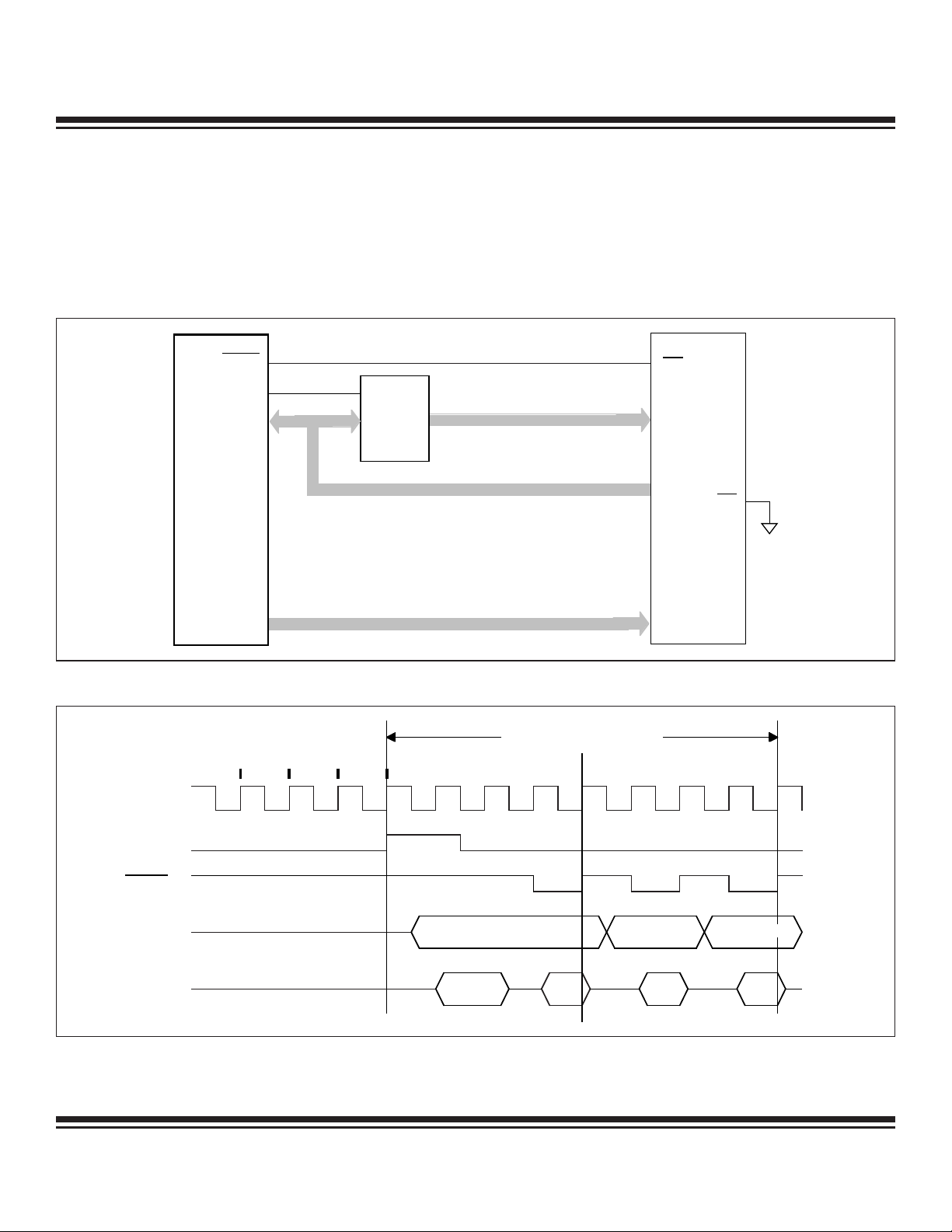
Internal Memory Cycles
C2 C3 C4 C1 C2 C1 C2
XTAL1
ALE
Port 0
Port 2
PSEN
C1
Ext Code Fetches
Page Miss Page Hit Page Hit
Data Data
LSB AddLSB Add LSB Add
DataMSB Add
PSEN
ALE
CK
74F373
LATCH
MSB ADDRESS
DATA BUS
LSB ADDRESS
PORT 0
(8)
(8)
64kB X 8
MEMORY
(8)
OE
CE
PORT 2
DS89C4x0
Ultra-High-Speed Flash
Microcontroller User’s Guide
Page Mode 2 Bus Structure
The page mode 2 external bus structure multiplexes the most significant address byte with data on P2 and uses P0 for the least significant address byte. An illustration of this memory interface is provided in Figure 6-6.
This bus structure speeds up external code fetches only. Aside from the different functions of P0 and P2 when operating in page mode
2, the external memory accesses are equal in duration and timing to those made in the nonpage mode. Figure 6-7 illustrates memory
cycles for the page mode 2 bus structure.
Figure 6-6. Program Memory Interconnect (Page Mode 2)
Figure 6-7. Page Mode 2 External Code Fetch Cycle (CD1:0 = 10b)
6-11
Maxim Integrated
Page 79

Ultra-High-Speed Flash
MD2: MD0 (STRETCH VALUE) STR ETCH CYCL ES 4X/2X, CD1, CD0 = 10 0 4X/2X, CD1 , CD0 = 00 0 4X /2X , CD1, CD0 = X10 4X/2X, CD1, CD0 = X11
000 0 0.5 1 2 204 8
001 1 1 2 4 40 9 6
010 2 2 4 8 81 9 2
011 3 3 6 12 12288
100 7 4 8 16 16384
101 8 5 10 20 20480
110 9 6 12 24 24576
111 10 7 14 28 286 72
Microcontroller User’s Guide
Data Memory Interface
As described in Section 4, the ultra-high-speed microcontroller provides a small amount of RAM mapped as registers for on-chip direct
access. This is not considered data memory and does not fall into the memory map. Systems that require more RAM or memorymapped peripherals must use the data memory area. This segment is a 64kB space located between 0000h and FFFFh. It is reached
using the MOVX instruction. Any use of this instruction automatically accesses the data area. Although the original 8051 convention
placed all data memory off-chip, the device incorporates 1kB of on-chip data memory. The means for enabling and accessing this
1kB SRAM was covered earlier in this section.
From a software standpoint, the physical location of the data area is not relevant because the same instructions are used. Like the program segment, if software accesses a data address that is above the on-chip data area, this access is automatically routed to the
expanded bus. Thus, data or peripherals that are off-chip can be used in conjunction with on-chip memory by selecting addresses
that do not overlap. For example, since the microcontroller has 1kB of on-chip data memory, an MOVX instruction at location 0400h is
directed off-chip through the expanded bus.
The external data memory interface follows the same bus structure as defined for program memory. The page mode enable (PAGEE)
and page mode select (PAGES 1:0) bits control whether the external bus structure follows the nonpage mode, page mode 1, or page
mode 2 scheme. During external data read/write operations, P0 or P2 (depending upon external memory mode) serves as the bidirectional data bus. This port is held in a high-impedance state for external reads from data memory, and driven with data during external
writes to data memory. The read and write strobes used to access external data memory are provided on P3.7 and P3.6, respectively.
External Data Memory Interface—Nonpage Mode
Data memory is accessed through use of the MOVX instruction. This instruction requires two basic memory cycles: a program-fetch
memory access and then a read or write memory access. Just like the program memory cycle, a basic internal data memory cycle
contains one system clock, and a basic external data memory cycle contains four system clocks for nonpage mode operation. The
program-fetch memory cycle for an MOVX instruction is no different from any other instruction. The unique timing occurs for the second memory cycle when data is accessed.
The ultra-high-speed flash microcontroller allows software to adjust the speed of external data memory access by stretching the memory bus cycle. The MD2:0 bits contained in the CKCON (8Eh) SFR provide the means to modify the stretch value. This stretch feature
allows the application to dynamically select the minimum (fastest) access time to each data memory peripheral device. The table below
shows the data memory cycle stretch values and their effect on the read and write control signals associated with the external MOVX
memory bus cycle. A stretch machine cycle always contains four system clocks.
As illustrated in Table 6-4, the stretch feature supports eight external data memory access cycles, which can be categorized into three
timing groups. When the stretch value is cleared to 000b, there is no stretch on external data memory access and a MOVX instruction
is completed in two basic memory cycles. When the stretch value is set to 001b, 010b, or 011b, the external data memory access is
extended by 1, 2, or 3 stretch machine cycles, respectively. Note that the 001b stretch value does not add four system clocks to the
RD or WR control signals but instead uses one system clock to create additional address setup and data bus float time and one system clock to cr
can be selected. In this stretch category, one stretch machine cycle (four system clocks) is used to stretch the ALE pulse width, one
stretch machine cycle is used to create additional setup, and one stretch machine cycle is used to cr
eate additional address and data hold time. When using very slow RAM and peripherals, a larger stretch value (4–7)
eate additional hold time.
Table 6-4. Nonpage Mode Data Memory Stretch Values
Maxim Integrated
6-12
Page 80

RD
(P3.7)
A
LE
CK
74F373
LATCH
LSB ADDRESS
DATA BUS
MSB ADDRESS
PORT 2
(8)
(8)
64kB X 8
SRAM
(8)
PORT 0
WR
(P3.6
)
OE
WE
CE
DS89C4x0
RD/W R PULSE WIDTH (IN NUM BE R O F OSCILLATO R C LO C KS)
MD2:M D0
(STRETC H VALUE)
STRETCH
CYCLES
4X/2X, CD1, CD0 = 100 4X/2X, CD1, CD0 = 000 4X/2X, CD1, CD0 = X10 4X/2X, CD1, CD0 = X11
000 0 0.25 0.5 1 1024
001 1 0.75 1.5 3 3072
010 2 1.75 3.5 7 7168
011 3 2.75 5.5 11 11264
100 7 3.75 7.5 15 15360
101 8 4.75 9.5 19 19456
110 9 5.75 11.5 23 23552
111 10 6.75 13.5 27 27648
Ultra-High-Speed Flash
Microcontroller User’s Guide
Figure 6-8. Data Memory Interconnect (Nonpage Mode)
External Data Memory Interface—Page Modes
The ultra-high-speed flash microcontroller allows software to adjust the speed of external data memory access by stretching the memory bus cycle in page mode operation just like nonpage mode operation. The tables below summarize the stretch values for page mode
1 and page mode 2. The number of stretch cycles added to the external MOVX operation and the control signal pulse width (in terms
of the number of oscillator clocks) are provided. A stretch machine cycle always contains four system clocks, independent of the logic
value of the page mode select bits.
Just like nonpage mode operation, the stretch feature supports eight stretched external data memory access cycles that can be categorized into three timing groups. When the stretch value is cleared to 000b, there is no stretch on external data memory access and
a MOVX instruction is completed in two basic memory cycles. When the stretch value is set to 001b, 010b, or 011b, the external data
memory access is extended by 1, 2, or 3 stretch machine cycles, respectively. The 001b stretch value does not add four system clocks
to the RD or WR control signals, but instead uses one system clock to create additional address setup and data bus float time and
uses one system clock to create additional address and data hold time. When using very slow RAM and peripherals, a larger stretch
value (4–7) can be selected. In this stretch category, one stretch machine cycle (four system clocks) is used to stretch the ALE pulse
width, one str
time.
Table 6-5. Page Mode 1—Data Memory Stretch Values 1 Cycle (PAGES 1:0 = 00b)
6-13
etch machine cycle is used to create additional setup and one stretch machine cycle is used to create additional hold
Maxim Integrated
Page 81

Ultra-High-Speed Flash
RD/W R PULSE WIDTH (IN NUM BE R O F OSCILLATO R C LO C KS)
MD2:M D0
(STRETC H VALUE)
STRETCH
CYCLES
4X/2X, CD1, CD0 = 100 4X/2X, CD1, C D0 = 000 4X/2X, CD1, CD0 = X10 4X/2X, CD 1, CD0 = X11
000 0 0.25 0.5 1 1024
001 1 0.75 1.5 3 3072
010 2 1.75 3.5 7 7168
011 3 2.75 5.5 11 11264
100 7 3.75 7.5 15 15360
101 8 4.75 9.5 19 19456
110 9 5.75 11.5 23 23552
111 10 6.75 13.5 27 27648
RD/WR PULSE WIDTH (I N NUMBE R OF OSCILLATOR CLOC KS )
MD2:M D0
(STRETC H VALUE)
STRETCH
CYCLES
4X/2X, CD1, CD0 = 100 4X/2X, CD1, CD0 = 000 4X/2X, CD1, CD0 = X10 4X/2X, CD1, CD0 = X11
000 0 0.5 1 2 2048
001 1 1 2 4 4096
010 2 2 4 8 8192
011 3 3 6 12 12288
100 7 4 8 16 16384
101 8 5 10 20 20480
110 9 6 12 24 24576
111 10 7 14 28 28672
RD/W R PULSE WIDTH (IN NUM BE R OF OSCILLATOR CLOC KS)
MD2:M D0
(STRETC H VALUE)
STRETCH
CYCLES
4X/2X, CD1, CD0 = 100 4X/2X, CD1, CD0 = 000 4X/2X, CD1, CD0 = X10 4X/2X, CD1, CD0 = X11
000 0 0.5 1 2 2048
001 1 1 2 4 4096
010 2 2 4 8 8192
011 3 3 6 12 12288
100 7 4 8 16 16384
101 8 5 10 20 20480
110 9 6 12 24 24576
111 10 7 14 28 28672
Microcontroller User’s Guide
Table 6-6. Page Mode 1—Data Memory Stretch Values Two Cycles (Pages 1:0 = 01b)
Table 6-7. Page Mode 1—Data Memory Stretch Values Four Cycles (Pages 1:0 = 10b)
Table 6-8. Page Mode 2—Data Memory Stretch Values (Pages 1:0 = 11b)
Maxim Integrated
6-14
Page 82

ALE
CK
74F373
LATCH
MSB ADDRESS
DATA BUS
LSB ADDRESS
PORT 0
(8)
(8)
64kB X 8
SRAM
(8)
PORT 2
RD
(P3.7)
WR
(P3.6
)
OE
WE
CE
DS89C4x0
ALE
CK
74F373
LATCH
MSB ADDRESS
LSB ADDRESS
DATA BUS
PORT 0
(8)
(8)
64kB X 8
SRAM
(8)
CE
PORT 2
RD
(P3.7)
WR
(P3.6
)
OE
WE
DS89C4x0
Ultra-High-Speed Flash
Microcontroller User’s Guide
Figures 6-9 and 6-10 show data memory interconnect examples for page mode 1 and page mode 2.
Figure 6-9. Data Memory Interconnect (Page Mode 1)
Figure 6-10. Data Memory Interface (Page Mode 2)
6-15
Maxim Integrated
Page 83

Ultra-High-Speed Flash
SYSCLK
ALE
PSEN
PORT2 MOVX MSB
LSB
MOVX INST INSTRUCTIONS
DATAPORT0
WR/RD
MOVX
DATA ACCESS
SYSCLK
ALE
PSEN
PORT2
PORT0
WR/RD
MOVX INST INSTRUCTIONS
MOVX DATA ACCESS
(1 STRETCH CYCLE)
= STRETCH CYCLE
MOVX MSB
MOVX DATAMOVX LSB
Microcontroller User’s Guide
Figures 6-11 to 6-22 illustrate the external data memory timing for the nonpage and page mode external bus structures.
Nonpage Mode Data Memory Timing
Figure 6-11 shows execution of the MOVX instruction from internal program memory with stretch value = 0 assigned (MD2:0 = 000b).
Note that the internal memory cycles consist of one system clock while the external memory cycles always consist of four system clocks.
Figure 6-12 illustrates the same MOVX instruction with a default stretch value (MD2:0 = 001b). The stretch cycle (four system clocks)
is distributed as follows: one system clock added for address setup, two system clocks being added to the RD or WR pulse duration,
and one system clock added for address/data hold. For subsequent stretch values of 2 or 3, the full stretch cycle is added to the duration of the RD or WR pulse.
Figure 6-11. Nonpage Mode: MOVX (Two Cycles)
Figure 6-12. Nonpage Mode: MOVX (Three Cycles)
Maxim Integrated
6-16
Page 84

Ultra-High-Speed Flash
SYSCLK
ALE
PSEN
PORT2
PORT0
WR/RD
MOVX MSB MOVX LSB
DATA
MOVX INST INSTRUCTIONS
MOVX DATA ACCESS
(PAGE MISS)
SYSCLK
ALE
PSEN
PORT2
PORT0
WR/RD
MOVX INST INSTINST
MOVX DATA ACCESS
(PAGE MISS + 1 STRETCH CYCLE)
MOVX MSB MOVX LSB
MOVX DATA
= STRETCH CYCLE
Microcontroller User’s Guide
Page Mode 1 Data Memory Timing–PAGES 1:0 = 10b (Four Cycles)
Figure 6-13 shows execution of the MOVX instruction from internal program memory with stretch value = 0 assigned (MD2:0 = 000b).
Note that the internal memory cycles consist of one system clock while the external memory cycles consist of four system clocks (page
hit) or eight system clocks (page miss).
Figure 6-14 illustrates the same MOVX instruction with a default stretch value (MD2:0 = 001b). The stretch cycle (four system clocks)
is distributed as follows: one system clock added for address setup, two system clocks being added to the RD or WR pulse duration,
and one system clock added for address/data hold. For subsequent stretch values of 2 or 3, the full stretch cycle is added to the duration of the RD or WR pulse.
Figure 6-13. Four-Cycle Page Mode 1: MOVX (Two Cycles)
Figure 6-14. Four-Cycle Page Mode 1: MOVX (Three Cycles)
6-17
Maxim Integrated
Page 85

Ultra-High-Speed Flash
SYSCLK
ALE
PSEN
PORT2
PORT0
WR/RD
MOVX #1
MSB
MOVX #1
LSB
MOVX #2
MSB
MOVX
DATA
MOVX
DATA
MOVX #2
LSB
MOVX#1MOVX
#2
INSTRUCTIONSINST
MOVX #1 DATA ACCESS
(PAGE MISS)
MOVX #2 DATA ACCESS
(PAGE MISS)
SYSCLK
ALE
PSEN
PORT2 MOVX MSB MOVX LSB
MOVX DATAPORT0
WR/RD
MOVX INST INSTRUCTIONS
MOVX DATA ACCESS
(PAGE MISS + 1 STRETCH CYCLE)
= STRETCH CYCLE
Microcontroller User’s Guide
Page Mode 1 Data Memory Timing–Pages 1:0 = 01b (Two Cycles)
Figure 6-15 below shows execution of back-to-back MOVX instructions from internal flash memory. A stretch value = 0 (MD2:0 = 000b)
has been assigned. Note that the internal memory cycles consist of one system clock while the external memory cycles consist of two
system clocks (page hit) or four system clocks (page miss).
Figure 6-16 illustrates the timing of the MOVX operation with stretch value = 1 (MD2:0 = 001b). The stretch cycle (four system clocks)
is distributed as follows: one system clock added for address setup, two system clocks being added to the RD or WR pulse duration,
and one system clock added for address/data hold. For subsequent stretch values of 2 or 3, the full stretch cycle is added to the duration of the RD or WR pulse.
Figure 6-15. Two-Cycle Page Mode 1: MOVX (Two Cycles)
Figure 6-16. Two-Cycle Page Mode 1: MOVX (Three Cycles)
Maxim Integrated
6-18
Page 86

Ultra-High-Speed Flash
SYSCLK
ALE
PSEN
PORT2 LSB LSB MSB LSBMOVX MSB MOVX LSB
MOVX DATAPORT0
WR/RD
MOVX INST
(PAGE HIT)
INST
(PAGE MISS)
MOVX DATA ACCESS
(PAGE MISS + 1 STRETCH CYCLE)
= STRETCH CYCLE
SYSCLK
ALE
PSEN
PORT2
PORT0
WR/RD
MOVX #1 INST
(PAGE HIT)
INST
(PAGE HIT)
INST
(PAGE HIT)
INST
(PAGE HIT)
= STRETCH CYCLE
MOVX LSBLSB LSB LSB LSBLSB
MOVX DATA
MOVX DATA ACCESS
(PAGE HIT + 1 STRETCH CYCLE)
Microcontroller User’s Guide
Page Mode 1 Data Memory Timing–Pages 1:0 = 01b (Two Cycles) (continued)
Figure 6-17 shows execution of a MOVX instruction with default stretch value = 1 (MD2:0 = 001b) from external program memory. The
most probable case, where a page-miss is needed for the MOVX instruction, is given here. However, if the MOVX address happened
to coincide with the current code execution page, a page hit would occur.
Figure 6-18 illustrates the MOVX timing that would occur if the address MSB for the MOVX data were to coincide with the code execution pages before and after the data access. Since a different MSB would not need to be latched, neither of the page-miss cycles
seen in the third diagram would occur.
Figure 6-17. Two-Cycle Page Mode 1: MOVX (Three Cycles) External Code Execution with Page Misses
Figure 6-18. Two-Cycle Page Mode 1: MOVX (Three Cycles) External Code Execution - No Page Misses
6-19
Maxim Integrated
Page 87

Ultra-High-Speed Flash
SYSCLK
ALE
PSEN
PORT2
MOVX
MSB
MOVX
MSB
MOVX DATAMOVX DATA
MOVX #1 LSB ADDRESS MOVX #2 LSB ADDRESS
PORT0
WR/RD
MOVX#1MOVX
#2
INST INST
= STRETCH CYCLE
MOVX #1 DATA ACCESS
(PAGE MISS + 1 STRETCH CYCLE)
MOVX #2 DATA ACCESS
(PAGE MISS + 1 STRETCH CYCLE)
SYSCLK
ALE
PSEN
PORT2
PORT0
WR/RD
MOVX#1MOVX
#2
INST INSTRUCTIONS
MOVX #1
DATA ACCESS
(PAGE MISS)
MOVX #2
DATA ACCESS
(PAGE MISS)
MOVX
MSB
MOVX
LSB
MOVX
MSB
MOVX
LSB
MOVX
DATA
MOVX
DATA
Microcontroller User’s Guide
Page Mode 1 Data Memory Timing–Pages 1:0 = 00b (One Cycle)
Figure 6-19 illustrates execution of back-to-back MOVX instructions from internal flash memory. The default MOVX stretch setting
(MD2:0 = 001b) has been assumed. The total duration of each MOVX instruction is seven system clocks = one system clock (pagehit memory cycle) + 2 system clocks (page-miss memory cycle) + four system clocks (one stretch cycle). Note that all external MOVX
operations in one-cycle page mode 1 result in page-misses.
Figure 6-20 illustrates execution of the same back-to-back MOVX instructions with a stretch value of 0 (MD2:0 = 000b).
Figure 6-19. One-Cycle Page Mode 1: MOVX (Three Cycles)—MOVX (Three Cycles)
Figure 6-20. One-Cycle Page Mode 1: MOVX (Two Cycles)—MOVX (Two Cycles)
Maxim Integrated
6-20
Page 88

Ultra-High-Speed Flash
SYSCLK
ALE
PSEN
PORT2 LSB LSB LSB
MOVX
MSB
MOVX
LSB
MOVX
MSB
MOVX#1MOVX
#2
MOVX #1
DATA ACCESS
(PAGE MISS)
MOVX #2
DATA ACCESS
(PAGE MISS)
INST
(PAGE MISS)
INST
(PAGE MISS)
INSTRUCTIONS
MOVX
LSB
MOVX
DATA
MOVX
DATA
MSBMSB LSB LSB LSB LSB LSB LSB LSB
PORT0
WR/RD
= STRETCH CYCLES
SYSCLK
ALE
PSEN
PORT2
PORT0
MOVX INST
WR/RD
Microcontroller User’s Guide
Page Mode 1 Data Memory Timing–Pages 1:0 = 00b (One Cycle) (continued)
Figure 6-21, still using a MOVX stretch value = 0, shows the back-to-back MOVX instructions being executed from external program
memory.
Figure 6-22 shows external code memory execution of an external MOVX instruction with stretch value = 4 (MD2:0 = 100b). It has been
assumed, for this example, that a page-miss is required for the MOVX data access. A stretch value = 4 results in the addition of 4
stretch cycles beyond the stretch value = 3. The four stretch cycles are distributed as folllows: two stretch cycles added for address
setup, one stretch cycle added to RD or WR pulse duration, and 1 stretch cycle added for address/data hold. For subsequent stretch
values of 5, 6, or 7, the added stretch cycle increases the RD or WR pulse duration.
Figure 6-21. One-Cycle Page Mode 1: MOVX (Two Cycles)—MOVX (Two Cycles) External Code Execution
Figure 6-22. One-Cycle Page Mode 1: MOVX (Nine Cycles) External Code Execution
6-21
Maxim Integrated
Page 89

Ultra-High-Speed Flash
Microcontroller User’s Guide
Page Mode 2 Data Memory Timing–Pages 1:0 = 11b (Four Cycles)
All external data memory accesses made using the page mode 2 external bus configuration require four system clocks. The MOVX
timing looks identical to the nonpage mode MOVX timing except that port 2 multiplexes the MSB and the data, while port 0 serves as
the LSB.
Data Memory Access
As mentioned earlier in this section, the ultra-high-speed microcontroller uses the MOVX instruction for data memory access. This
includes off-chip RAM and memory-mapped peripherals needing read/write access. Several aspects of the MOVX operation have been
enhanced as compared to the original 8051. The principal improvements are in the areas of the MOVX timing and the data pointer.
The MOVX instruction is used to generate read/write access to off-chip address locations. It has several addressing modes. The first
uses the MOVX @Ri command to reach a 256-byte block. This instruction uses the value in the designated working register to address
one of 256 locations. The upper byte of the address is supplied by the value in the port 2 latch. A second way to access data is the
data pointer (DPTR). This 16-bit register provides an absolute address for data memory access. 16-bits cover the entire 64kB area.
Thus the DPTR serves as a pointer to memory. Using the DPTR, the relevant instruction is MOVX @DPTR.
The original 8051 contained one DPTR. While this pr
address to another. The ultra-high-speed microcontroller provides two data pointers. Thus softwar
tination address. The MOVX instruction uses the active pointer to direct the off-chip address.
The dual data pointers are DPTR0 and DPTR1. DPTR0 is at SFR addresses 82h and 83h. These are the locations used by the original
8051. No modification of standard code is needed to use DPTR0. The new DPTR is located at SFR 84h and 85h. The data pointer select
bit (SEL) chooses the active pointer and is located in bit position 0 of the DPS (86h) SFR. When DPS is set to 0, the DPTR0 is active.
When set to 1, DPTR1 is used. All DPTR-related instructions use the currently selected DPTR for any activity.
Each data pointer (DPTR0, DPTR1) has an associated control bit (ID0, ID1) that determines whether the INC DPTR operation results in
an increment or decrement of the pointer. When the active data pointer ID (increment/decrement) control bit is clear, the INC DPTR
instruction will increment the pointer, whereas a decrement occurs if the active pointer’s ID bit is set when the INC DPTR instruction is
performed.
ID0 = DPS.6
ID1 = DPS.7
Using the dual data pointers for large block copy operations results in substantial code savings versus using a single data pointer,
since one data pointer can be used for the source address and the second pointer can be used as the destination address. The user
switches between data pointers by toggling the SEL bit. One way of accomplishing this is by executing the INC DPS instruction. For
these large-block copy operations, the user must execute this instruction frequently to toggle between DPTR0 and DPTR1. To improve
the speed and efficiency of moving data with dual data pointers, the ultra-high-speed microcontroller contains a toggle select (TSL)
bit. When this TSL bit (DPS.5) is set, execution of certain MOVX instructions automatically toggle the SEL bit in hardware, allowing
removal of the INC DPS instruction and increasing execution speed.
Copying large blocks of data also requires that the source and destination pointers index byte-by-byte through their respective data
ranges. The traditional method for incrementing each pointer is through the use of the INC DPTR instruction. The ultra-high-speed flash
microcontroller provides yet another means of accelerating data transfers with the implementation of an auto increment/decrement bit
(AID). When this AID bit (DPS.4) is set, execution of certain MOVX instructions automatically increments or decrements the active data
pointer.
AUTO-TOGGLE (if TSL = 1)
MOVC A, @A+DPTR MOVC A, @A+DPTR
MOVX A, @DPTR MOVX A, @DPTR
MOVX @DPTR, A MOVX @DPTR, A
INC DPTR
MOV DPTR, #data16
Table 6-9 summarizes the tremendous speed improvements gained through using the dual DPTRs along with autoincrement and autotoggle features. To properly quantify the speed improvement gained with enhanced data pointer operation versus improvement attributed to the single-cycle core architecture, execution time for the DS80C320 high-speed microcontroller (four-cycle core) has been
included where applicable. For external page mode 1 (PAGES1:0 = 00b) code execution has been assumed. It is unreasonable to
expect that the address MSBs for MOVX read/write operations are the same as the address MSB for code execution. Ther
ovides access to the entire memory area, it is difficult to move data from one
e can load both a source and a des-
AUTO-INC/DEC (if AID = 1)
efore, one
Maxim Integrated
6-22
Page 90

Ultra-High-Speed Flash
Microcontroller User’s Guide
clock cycle has been added to each MOVX instruction (for data access) and to the instruction that follows the MOVX (for code fetch)
to account for potential page misses. The sample code listings have been marked accordingly with ‘+D’ to indicate a data access
page-miss and ‘+C’ to indicate a code-fetch page-miss. Thus, in the case of back-to-back MOVX operations, the second MOVX operation has two clock cycles added (‘+CD’), one associated with the code fetch and one associated with the data access.
Table 6-9. Enhanced Data Pointer Speed Improvement
DS80C32 0 HIGH SP EED DS89C4 2 0 ULTRA-HIGH S P EED
DATA POINTER OP ERATION
Single Dat a Poi n t er 1869 x 4 22 7 µ s 19 3 3 59µs
Dual Da ta Po i nt er 1098 x 4 13 3 µ s 12 9 1 39µ s
Dual Dat a Po i nt er w/ AID — — 11 6 9 35µ s
Dual Da ta Po i nt er w/TSL — — 910 28 µ s
Dual Da ta Po i nt er w/ AID,TS L — — 782 24µ s
The sample code listings for these programs appear on the following pages.
Program 1 listed below is original code written for an 8051 and utilizes a single data pointer.
Program 2 uses the dual data pointer feature.
Program 3 uses the dual data pointer with autoincr
Program 4 uses the dual data pointer with autotoggle enhancement.
Program 5 uses the dual data pointer with autoincrement and autotoggle enhancements.
CLOCK CYCLES
(4CLKS/MCLK)
EXE CUTION TIME
(AT 33MHZ)
ement enhancement.
CLOCK CYCLES
EXE CUTION TIME
(AT 33MHZ)
The relevant register and bit locations are summarized as follows:
DPL 82h Low-byte original DPTR
DPH 83h High-byte original DPTR
DPL1 84h
Low-byte new DPTR
DPH1 85h High-byte new DPTR
DPS 86h SEL bit = DPS.0
AID bit = DPS.4
TSL bit = DPS.5
PROGRAM 1: 64-BYTE BLOCK MOVE (WITHOUT DUAL DATA POINTER)
; SH and SL are high and low byte source address.
; DH and DL are high and low byte of destination address.
; For cycle counts:
; HSM = High-Speed Microcontroller
; UHSM = ultra-high-speed microcontroller
# HSM/UHSM CYCLES
MOV R5, #64 ; NUMBER OF BYTES TO MOVE 2/2
MOV DPTR, #SHSL ; LOAD SOURCE ADDRESS 3/3
MOV R1, #SL ; SAVE LOW BYTE OF SOURCE 2/2
MOV R2, #SH ; SAVE HIGH BYTE OF SOURCE 2/2
MOV R3, #DL ; SAVE LOW BYTE OF DESTINATION 2/2
MOV R4, #DH ; SAVE HIGH BYTE OF DESTINATION 2/2
MOVE:
6-23
Maxim Integrated
Page 91

Ultra-High-Speed Flash
Microcontroller User’s Guide
; THIS LOOP IS PERFORMED R5 TIMES, IN THIS EXAMPLE 64
MOVX A, @DPTR ; READ SOURCE DATA BYTE 2/3 +D
MOV R1, DPL ; SAVE NEW SOURCE POINTER 2/3 +C
MOV R2, DPH ; 2/2
MOV DPL, R3 ; LOAD NEW DESTINATION 2/2
MOV DPH, R4 ; 2/2
MOVX @DPTR, A ; WRITE DATA TO DESTINATION 2/3 +D
INC DPTR ; NEXT DESTINATION ADDRESS 3/2 +C
MOV R3, DPL ; SAVE NEW DESTINATION POINTER 2/2
MOV R4, DPH ; 2/2
MOV DPL, R1 ; GET NEW SOURCE POINTER 2/2
MOV DPH, R2 ; 2/2
INC DPTR ; NEXT SOURCE ADDRESS 3/1
DJNZ R5, MOVE ; FINISHED WITH TABLE? 3/4
PROGRAM 2: 64-BYTE BLOCK MOVE (DUAL DATA POINTER)
; SH and SL are high and low byte source address.
; DH and DL are high and low byte of destination address.
; DPS is the data pointer select. Reset condition DPTR0.
; For cycle counts:
; HSM = High-Speed Microcontroller
; UHSM = ultra-high-speed microcontroller
DPS EQU 86h ; TELL ASSEMBLER ABOUT DPS
MOV R5, #64 ; NUMBER OF BYTES TO MOVE 2/2
MOV DPTR, #DHDL ; LOAD DESTINATION ADDRESS 3/3
INC DPS ; CHANGE ACTIVE DPTR 2/3
MOV DPTR, #SHSL ; LOAD SOURCE ADDRESS 3/3
MOVE:
; THIS LOOP IS PERFORMED R5 TIMES, IN THIS EXAMPLE 64
MOVX A, @DPTR ; READ SOURCE DATA BYTE 2/3 +D
INC DPS ; CHANGE DPTR TO DESTINATION 2/4 +C
MOVX @DPTR, A ; WRITE DATA TO DESTINATION 2/3 +D
INC DPTR ; NEXT DESTINATION ADDRESS 3/2 +C
INC DPS ; CHANGE DATA POINTER TO SOURCE 2/3
INC DPTR ; NEXT SOURCE ADDRESS 3/1
DJNZ R5, MOVE ; FINISHED WITH TABLE? 3/4
# HSM/UHSM CYCLES
# HSM/UHSM CYCLES
PROGRAM 3: 64-BYTE BLOCK MOVE (DUAL DATA POINTER, AID)
; SH and SL are high and low byte source address.
; DH and DL are high and low byte of destination address.
; DPS is the data pointer select. Reset condition DPTR0.
DPS EQU 86h ; TELL ASSEMBLER ABOUT DPS
MOV R5, #64 ; NUMBER OF BYTES TO MOVE 2
ORL DPS, #10h ; SET AUTO-INC/DEC (AID) 3
MOV DPTR, #DHDL ; LOAD DESTINATION ADDRESS 3
INC DPS ; CHANGE ACTIVE DPTR 3
MOV DPTR, #SHSL ; LOAD SOURCE ADDRESS 3
MOVE:
Maxim Integrated
# UHSM CYCLES
6-24
Page 92

Ultra-High-Speed Flash
Microcontroller User’s Guide
; THIS LOOP IS PERFORMED R5 TIMES, IN THIS EXAMPLE 64
MOVX A, @DPTR ; READ SOURCE DATA BYTE 3 +D
INC DPS ; CHANGE DPTR TO DESTINATION 4 +C
MOVX @DPTR, A ; WRITE DATA TO DESTINATION 3 +D
INC DPS ; CHANGE DATA POINTER TO SOURCE 4 +C
DJNZ R5, MOVE ; FINISHED WITH TABLE? 4
ANL DPS, #0EFH ; CLEAR AUTO-INC/DEC 3
PROGRAM 4: 64-BYTE BLOCK MOVE (DUAL DATA POINTER, TSL)
; SH and SL are high and low byte source address.
; DH and DL are high and low byte of destination address.
; DPS is the data pointer select. Reset condition DPTR0.
DPS EQU 86h ; TELL ASSEMBLER ABOUT DPS
MOV R5, #64 ; NUMBER OF BYTES TO MOVE 2
ORL DPS, #20h ; SET TOGGLE SELECT (TSL) 3
MOV DPTR, #SHSL ; LOAD SOURCE ADDRESS 3
MOV DPTR, #DHDL ; LOAD DESTINATION ADDRESS 3
MOVE:
; THIS LOOP IS PERFORMED R5 TIMES, IN THIS EXAMPLE 64
MOVX A, @DPTR ; READ SOURCE DATA BYTE 3 +D
MOVX @DPTR, A ; WRITE DATA TO DESTINATION 4 +CD
INC DPTR ; NEXT SOURCE ADDRESS 2 +C
INC DPTR ; NEXT DESTINATION ADDRESS 1
DJNZ R5, MOVE ; FINISHED WITH TABLE? 4
ANL DPS, #0DFh ; CLEAR TOGGLE SELECT 3
# UHSM CYCLES
PROGRAM 5: 64-BYTE BLOCK MOVE (DUAL DATA POINTER, AID, TSL)
; SH and SL are high and low byte source address.
; DH and DL are high and low byte of destination address.
; DPS is the data pointer select. Reset condition DPTR0.
# UHSM CYCLES
DPS EQU 86h ; TELL ASSEMBLER ABOUT DPS
MOV R5, #64 ; NUMBER OF BYTES TO MOVE 2
ORL DPS, #30h ; SET TOGGLE SELECT, AUTO-INC/DEC 3
MOV DPTR, #SHSL ; LOAD SOURCE ADDRESS 3
MOV DPTR, #DHDL ; LOAD DESTINATION ADDRESS 3
MOVE:
; THIS LOOP IS PERFORMED R5 TIMES, IN THIS EXAMPLE 64
MOVX A, @DPTR ; READ SOURCE DATA BYTE 3 +D
MOVX @DPTR, A ; WRITE DATA TO DESTINATION 4 +CD
DJNZ R5, MOVE ; FINISHED WITH TABLE? 5 +C
ANL DPS, #0CFh ; CLEAR TSL, AID 3
Note that since each pass through the loop saves additional clock cycles when compared to the single DPTR approach, efficiency
improvement when moving larger blocks is even greater using these features. Further speed improvement can be gained when executing from internal flash program memory
internal memory at 33MHz would require only 19.8µs (= 1/33MHz x (14 + 64 x 10)).
, since no code-fetch page misses (+C) would occur. For example, running Program 5 from
6-25
Maxim Integrated
Page 93

Ultra-High-Speed Flash
Microcontroller User’s Guide
SECTION 7: POWER MANAGEMENT
This section contains the following information:
Power Management Summary . . . . . . . . . . . . . . . . . . . . . . . . . . . . . . . . . . . . . . . . . . . . . . . . . . . .7-3
Precision Voltage Monitor . . . . . . . . . . . . . . . . . . . . . . . . . . . . . . . . . . . . . . . . . . . . . . . . . . . .7-4
Early-Warning Power-Fail Interrupt . . . . . . . . . . . . . . . . . . . . . . . . . . . . . . . . . . . . . . . . . . . . .7-4
Power-Fail Reset . . . . . . . . . . . . . . . . . . . . . . . . . . . . . . . . . . . . . . . . . . . . . . . . . . . . . . . . . . .7-5
Power-On Reset . . . . . . . . . . . . . . . . . . . . . . . . . . . . . . . . . . . . . . . . . . . . . . . . . . . . . . . . . . .7-5
Bandgap Select . . . . . . . . . . . . . . . . . . . . . . . . . . . . . . . . . . . . . . . . . . . . . . . . . . . . . . . . . . .7-5
Watchdog Wake-Up From Idle . . . . . . . . . . . . . . . . . . . . . . . . . . . . . . . . . . . . . . . . . . . . . . . .7-5
Power Saving . . . . . . . . . . . . . . . . . . . . . . . . . . . . . . . . . . . . . . . . . . . . . . . . . . . . . . . . . . . . . . . . .7-6
Clock Divide Control . . . . . . . . . . . . . . . . . . . . . . . . . . . . . . . . . . . . . . . . . . . . . . . . . . . . . . . .7-6
Idle Mode . . . . . . . . . . . . . . . . . . . . . . . . . . . . . . . . . . . . . . . . . . . . . . . . . . . . . . . . . . . . . . . .7-7
Stop Mode . . . . . . . . . . . . . . . . . . . . . . . . . . . . . . . . . . . . . . . . . . . . . . . . . . . . . . . . . . . . . . .7-7
Ring Oscillator Wake-Up From Stop . . . . . . . . . . . . . . . . . . . . . . . . . . . . . . . . . . . . . . . . . . .7-8
Speed Reduction . . . . . . . . . . . . . . . . . . . . . . . . . . . . . . . . . . . . . . . . . . . . . . . . . . . . . . . . . .7-8
Power Management Modes . . . . . . . . . . . . . . . . . . . . . . . . . . . . . . . . . . . . . . . . . . . . . . . . . .7-9
Power Management Mode Timing . . . . . . . . . . . . . . . . . . . . . . . . . . . . . . . . . . . . . . . . . . . . .7-10
PMM and Peripheral Functions . . . . . . . . . . . . . . . . . . . . . . . . . . . . . . . . . . . . . . . . . . . . . . .7-10
Switchback . . . . . . . . . . . . . . . . . . . . . . . . . . . . . . . . . . . . . . . . . . . . . . . . . . . . . . . . . . . . . . . . . . .7-11
Clock Source Selection . . . . . . . . . . . . . . . . . . . . . . . . . . . . . . . . . . . . . . . . . . . . . . . . . . . . . . . . .7-12
Ring Oscillator Resume From Stop . . . . . . . . . . . . . . . . . . . . . . . . . . . . . . . . . . . . . . . . . . . . . . . .7-12
7-1
Maxim Integrated
Page 94

Ultra-High-Speed Flash
Microcontroller User’s Guide
LIST OF FIGURES
Figure 7-1. Power Cycle Operaton . . . . . . . . . . . . . . . . . . . . . . . . . . . . . . . . . . . . . . . . . . . . . . . . .7-4
Figure 7-2. System Clock Sources . . . . . . . . . . . . . . . . . . . . . . . . . . . . . . . . . . . . . . . . . . . . . . . . .7-6
Figure 7-3. Internal Timing Relationships in PMM . . . . . . . . . . . . . . . . . . . . . . . . . . . . . . . . . . . . .7-10
LIST OF TABLES
Table 7-1. Pin States in Power-Saving Modes . . . . . . . . . . . . . . . . . . . . . . . . . . . . . . . . . . . . . . . .7-8
Table 7-2. Crystal vs. MIPS Comparison . . . . . . . . . . . . . . . . . . . . . . . . . . . . . . . . . . . . . . . . . . . .7-8
Table 7-3. Power Management and Status Bit Summary . . . . . . . . . . . . . . . . . . . . . . . . . . . . . . .7-9
Table 7-4. Effect of PMM Clock Mode on Timer, Serial Operation . . . . . . . . . . . . . . . . . . . . . . . . .7-10
Table 7-5. Clock Control and Status Bit Summary . . . . . . . . . . . . . . . . . . . . . . . . . . . . . . . . . . . . .7-12
Maxim Integrated
7-2
Page 95

Ultra-High-Speed Flash
Microcontroller User’s Guide
SECTION 7: POWER MANAGEMENT
The ultra-high-speed flash microcontroller has several features that relate to power consumption and management. They provide a
combination of controlled operation in unreliable power applications and reduced power consumption in portable or battery-powered
applications. The range of features is shown below with details to follow.
POWER MANAGEMENT
Precision Voltage Monitor
Early-Warning Power-Fail Interrupt
Power-Fail/Power-On Reset
Bandgap Select
Watchdog Wake-Up From Idle
POWER SA
VING
Clock Divide Control
Idle Mode
Stop Mode
Ring Wake-Up From Stop
Power Management Mode
Power Management Summary
The following is a summary of the power management bits and those that are useful or related. They are contained in the register locations WDCON;D8h, EIE;E8h, EXIF;91h, and PCON; 87h.
WDCON.6 POR: Power-on reset. Hardware sets this bit on a power-up condition. Software can read it but must clear it man-
ually. This bit assists software in determining the cause of a reset.
WDCON.5 EPFI: enable power-fail interrupt. Setting this bit to 1 enables the power-fail interrupt. This occurs when V
to approximately 4.375V and the processor vectors to location 33h. Setting this bit to a 0 turns off the power-fail interrupt.
WDCON.4 PFI: Power-fail interrupt flag. Hardware sets this bit to a 1 when a power-fail condition occurs. Software must clear the
bit manually. Writing a 1 to this bit forces an interrupt, if enabled.
WDCON.3 WDIF: Watchdog interrupt flag. If the watchdog interrupt is enabled (EIE.4), hardware sets this bit to indicate that
the watchdog interrupt has occurred. If the interrupt is not enabled, this bit indicates that the timeout has passed. If
the watchdog reset is enabled (WDCON.1), the user has 512 system clocks to strobe the watchdog prior to a reset.
Softwar
WDCON.2 WTRF: Watchdog timer reset flag. Hardware sets this bit when the watchdog timer causes a reset. Softwar
it but must clear it manually. A power-fail reset also clears the bit. This bit assists software in determining the cause of
a reset. If EWT = 0, the watchdog timer has no effect on this bit.
WDCON.1 EWT: Enable watchdog timer reset. Setting this bit turns on the watchdog timer reset function. The interrupt does not
occur unless the EWDI bit in the EIE register is set. A r
register. Setting this bit to a 0 disables the resets but leaves the timer running.
WDCON.0 RWT: Reset watchdog timer. This bit serves as the strobe for the watchdog function. During the timeout period, soft-
war
elapsed. There is no need to set the RWT bit to a 0 because it is self-clearing.
EIE.4 EWDI: Enable watchdog interrupt. Setting this bit in software enables the watchdog interrupt.
EXIF.0 BGS: Bandgap select. Setting this bit to a 1 allows the use of the bandgap voltage reference while in stop mode. Since
this function uses as much as 75µA, the bandgap is optional in stop mode. Setting this bit to a 0 turns off the bandgap
while in stop mode. When BGS = 0, no power
PCON.1 STOP. When this bit is set, the program stops execution, clocks are stopped, and the CPU enters power-down mode.
PCON.0 IDLE. Program execution halts, leaving timers, serial por
e or any reset can clear this flag.
eset occurs according to the WD1 and WD0 bits in the CKCON
e must set the RWT bit if the watchdog is enabled. Failing to set the RWT causes a reset when the timeout has
-fail interrupt or power
ts, and clocks running.
-fail reset is available in stop mode.
drops
CC
e can read
7-3
Maxim Integrated
Page 96

Ultra-High-Speed Flash
V
CC
V
PFW
V
RST
V
SS
INTERRUPT
SERVICE ROUTINE
INTERNAL RESET
XTAL1
t
POR
t
CSU
Microcontroller User’s Guide
EXIF.2 RGMD: Ring oscillator mode. Hardware sets this status bit to a 1 when the clock source is the ring oscillator.
Hardware sets this status bit to a 0 when the crystal is the clock source. Refer to RGSL for operation of the ring oscillator.
EXIF.1 RGSL: Ring oscillator select. When set to a 1 by software, the microcontroller uses a ring oscillator to come out of
stop mode without waiting for crystal startup. This allows an instantaneous startup when coming out of stop mode. It
is useful if software needs to perform a short task, and then return to stop. It is also useful if software must respond
quickly to an exter
clocksource. The RGMD status bit reports on this changeover. When RGSL is set to a 0, the microcontroller delays
software execution until after the 65,536 clock crystal startup time. RGSL is only cleared by a power-on reset and is
not altered by other forms of reset.
Precision Voltage Monitor
A precision bandgap reference and other analog circuits monitor the state of the power supply during power-up and power-down transitions. This obviates the need for external circuits to perform these functions that other microcontroller systems would require. The
bandgap reference provides a precise voltage to compare with VCC. When VCCbegins to drop, the power monitor compares it to its
reference. This enables the analog circuits to detect when V
specified in the product data sheet.
Early-Warning Power-Fail Interrupt
The precision voltage reference has the ability to generate a power-fail interrupt and/or reset in response to a low-supply voltage. When
reaches the V
V
CC
allows the system time to save critical parameters in nonvolatile memory and put external functions in a safe state.
The power-fail interrupt is optional and is enabled using the enable power-fail warning interrupt (EPFI) bit at WDCON.5. If enabled, V
dropping below V
VCC transitions below V
it. As long as the condition exists, PFI is immediately set again by hardware.
threshold, the microcontroller can generate a power-fail interrupt. This early warning of supply voltage failure
PFW
causes the device to vector to address 33h. The power-fail interrupt status bit, PFI (WDCON.4), is set anytime
PFW
PFW
nal event. After the crystal has performed 65,536 cycles, hardware switches to the crystal as its
passes through predetermined thresholds, V
CC
. This flag is not cleared when VCCis above V
, and software should clear it immediately after reading
PFW
PFW
and V
. These are
RST
CC
Figure 7-1. Power Cycle Operaton
Maxim Integrated
7-4
Page 97

Ultra-High-Speed Flash
Microcontroller User’s Guide
A typical application of the PFI is to place the device into a “safe mode” when a power loss appears imminent. When the interrupt
occurs, the code vectors to location 33h. At this time, software can disable the interrupt, save any critical data, clear PFI, and then continually poll the status of the power supply through the PFI flag. As long as PFI is set, power is still below V
proper level, PFI is not set once cleared by software. This indicates a safe operating condition. If power continues to fall, a power-fail
reset is invoked automatically.
Power-Fail Reset
The power-fail reset automatically invokes a reset when VCCdrops below V
their reset state. This state continues to be held until V
lower than V
device halts operation with a power-fail reset. The power-fail reset function cannot be disabled.
, the microcontroller has the option to use the power-fail interrupt to place the device into a “safe” state before the
PFW
drops below the voltage necessary to power the port pins. Because V
CC
. This halts device operation and places all outputs in
RST
Power-On Reset
When VCCis applied to a system, the device holds itself in reset until power is within tolerance and stable. The internal bandgap reference provides a highly accurate and stable means of detecting power-supply levels. It requires no external circuits to accomplish
this. As power rises, the processor stays in a reset state until VCC> V
this and activate the on-chip crystal oscillator. On-chip hardware then counts 65536 oscillator clocks. During this count, VCCmust
remain above V
period is used to make certain that power is within tolerance and that the oscillator has time to stabilize. This provides a very controlled
and predictable startup condition.
Once the 65536 count period has elapsed, the reset condition is removed automatically and software execution begins at the reset
vector location of 0000h. Software is able to detect the power-on reset condition using the power-on reset (POR) flag. POR is located
at WDCON.6. This bit is high to indicate that a power-on reset has occurred. It should then be cleared by software.
The complete power cycle operation is shown in Figure 7-1. Note that the interrupt threshold is fixed, but the interrupt itself is optional. Reset thresholds are also fixed and the reset operation is transparent. It requires no external components and no action by software
to control reset operation.
or the process restarts. If an off-chip clock source is used, clock counting still begins once V
RST
. As VCCrises above V
RST
, internal analog circuits detect
RST
. If power returns to the
PFW
> V
CC
. This count
RST
RST
is
Bandgap Select
The bandgap is normally disabled automatically upon entering stop mode to provide the lowest power state. Since the bandgap is
inactive, there can be no power-fail interrupt and no power-fail reset, similar to a traditional 8051.
If the use of the power-fail features is desired in stop mode, the BGS bit (EXIF, 91h) can be used. When set to a logic 1 by software,
the bandgap reference and associated power monitor circuits remain active in stop mode. The price of this feature is higher powersupply current requirements. In stop mode with the bandgap reference disabled (default), the processor draws approximately 10µA.
With the bandgap enabled, it draws approximately 75µA.
BGS allows the user to decide whether the control circuitry and its associated power consumption are needed. If the application is
such that power does not fail while in stop, or if it does not matter that power fails, the BGS should be set to 0 (default). If power can
fail at any time and cause problems, the BGS should be set to 1.
Watchdog Wake-Up From Idle
The watchdog wake-up is more of an application than a feature. It allows a system to enter the idle mode for power savings, then to
wake up periodically to sample the external world. Idle mode is a low-power state described below. Any of the programmable timers
can perform this function, but the watchdog allows a much longer period to be selected. At 33MHz, the maximum watchdog timeout
is over 2s. This contrasts with 23.8ms using the 16-bit timers. Software that uses the watchdog as a wake-up alarm should enable only
the watchdog interrupt and not the reset. Note that the watchdog cannot be used to wake the system while in stop mode since no
clocks are running. Stop mode is described in the Power Management Summary section.
7-5
Maxim Integrated
Page 98

Ultra-High-Speed Flash
4X/2X
CTM
Crystal
Oscillator
Divide-by-1024
Ring
Oscillator
Clock
Multiplier
CD0
CD1
Selector
Ring
Enable
MUX
System
Clock
Microcontroller User’s Guide
Power Saving
The ultra-high-speed flash microcontroller is implemented using full CMOS circuitry for low-power operation. It is fully static, so the
clock speed can be run down to DC. Like other CMOS, the power consumption is also a function of operating frequency. Although the
microcontroller is designed for maximum performance, it also provides improved power versus work relationships compared with standard 8051 devices. These topics are discussed in detail in the following pages.
Clock Divide Control
The programmable clock divide control bits CD1 and CD0 (PMR, C4h) provide the processor with the ability to adapt to different crystals and also to slow the system clocks, providing lower power operation when required. An on-chip crystal multiplier allows the ultrahigh-speed flash microcontroller to operate at two or four times the crystal frequency by setting the 4X/2X bit and is enabled by setting the CTM bit to a logic 1. An additional circuit provides a clock source at divide-by-1024. When used with a 10MHz crystal, for
example, the processor executes machine cycle in times ranging from 25ns (divide-by-0.25) to 102.4µs (divide-by-1024) and maintains a highly accurate, serial port baud rate while allowing the use of more cost-effective, lower-fr
divide control bits can be written at any time, certain hardware features have been provided to enhance the use of these clock controls to guarantee proper serial port operation, and also to allow for a high-speed response to an external interrupt. The 01b setting of
CD1 and CD0 is reserved and has the same effect as the setting of 10b, which forces the system clock into a divide-by-1 mode. The
ultra-high-speed flash microcontroller defaults to divide-by-1 clock mode on all forms of reset.
When programmed to the divide-by-1024 mode, and the switchback bit (PMR.5: SWB) is also set, the system forces the clock divide
control bits to reset automatically to the divide-by-1 mode whenever the system has detected externally enabled interrupts.
The oscillator divide ratios of 0.25, 0.5 and 1 are also used to provide standard baud rate generation for the serial ports through a
forced divide-by-12 input clocks (TxMH,TxM = 00b, x = 1, 2, or 3) to the timers. When in divide-by-1024 mode, in order to allow a quick
response to incoming data on a serial port, the system utilizes the switchback mode to automatically revert to divide-by-1 mode whenever a start bit is detected. This automatic switchback is only enabled during divide-by-1024 mode and all other clock modes are unaffected by interrupts and serial port activity. See Power Management Modes for more details.
equency crystals. Although the clock
Figure 7-2. System Clock Sources
Maxim Integrated
7-6
Page 99

Ultra-High-Speed Flash
Microcontroller User’s Guide
Use of the divide-by-0.25 or 0.5 option through the clock divide control bits requires that the crystal multiplier be enabled and the specific system clock multiply value be established by the 4X/2X bit in the PMR register. The multiplier is enabled by the CTM (PMR.4) bit
but cannot be automatically selected until a startup delay has been established through the CKRY bit in the status register. The 4X/2X
bit can only be altered when the CTM bit is cleared to a logic 0. This prevents the system from changing the multiplier until the system
has moved back to the divide-by-1 mode and the multiplier has been disabled through the CTM bit. The CTM bit can only be alter
when the CD1 and CD0 bits are set to divide-by-1 mode and the RGMD bit is cleared to 0. Setting the CTM to a logic 1 from a previous logic 0 automatically clears the CKRY bit in the status register and starts the multiplier startup timeout in the multiplier star
counter. During the multiplier startup period, the CKRY bit remains cleared and the CD1 and CD0 clock controls cannot be set to 00b.
The CTM bit is cleared to a logic 0 on all resets. Figure 7-2 (System Clock Sources) gives a simplified description of the generation of
the system clocks. Specifics of hardware restrictions associated with the use of the 4X/2X, CTM, CKRY, CD1, and CD0 bits are outlined in the SFR description.
The micr
its and drawbacks. These modes are idle and stop. In the original 8051, the stop mode is called power-down. These modes are invoked
in the same manner as the original 8051 series.
ocontroller provides two modes (other than operating) that allow power conservation. They are similar, but have different mer-
Idle Mode
Idle mode suspends all CPU processing by holding the program counter in a static state. No program values are fetched and no processing occurs. This saves considerable power versus full operation. The virtue of idle mode is that it uses half the power of the operating state, yet reacts instantly to any interrupt conditions. All clocks remain active so the timers, watchdog, serial port, and power monitor functions are all working. Since all clocks are running, the CPU can exit the idle state using any of the interrupt sources.
Software can invoke the idle mode by setting the IDLE bit in the PCON register at location 87h. The bit is located at PCON.0. The
instruction that executes this step is the last instruction prior to freezing the program counter. Once in idle, all resources are preserved.
There are two ways to exit the idle mode. First, any interrupt (that is enabled) will cause an exit. This results in a jump to the appropriate interrupt vector. The IDLE bit in the PCON register is cleared automatically. Upon returning from this vector using the RETI instruction, the next address is the one immediately after the instruction that invoked the idle state.
The idle mode can also be removed using a reset. Any of the three reset sources can do this. On receiving the reset stimulus, the CPU
is placed in a reset state and the idle condition cleared. When the reset stimulus is removed, software begins execution as for any
reset. Since all clocks are active, there is no delay after the reset stimulus is removed. Note that if enabled, the watchdog timer continues to run during idle and must be supported.
ed
tup
Stop Mode
Stop mode is the lowest power state available. This is achieved by stopping all on-chip clocks, resulting in a fully static condition. No
processing is possible, timers are stopped, and no serial communication is possible. Software can invoke stop mode by setting the
STOP bit in the PCON register at location 87h. The bit is located at PCON.1. Processor operation halts on the instruction that sets the
STOP bit. The internal amplifier that excites the external crystal is disabled, halting crystal oscillation in stop mode. Stop mode takes
precedence if application code attempts to set both the STOP and IDLE bits. However, doing this is not suggested. Table 7-1 shows
the state of the processor pins in idle and stop modes.
Stop mode can be exited in two ways. First, like the 8052 microcontrollers, a nonclocked interrupt such as the external interrupts or
the power-fail interrupt can be used. Clocked interrupts, such as the watchdog timer, internal timers, and serial ports do not operate
in stop mode. Note that the bandgap reference must be enabled in order to use the power-fail interrupt to exit stop mode, which
increases stop mode current. Processor operation resumes with the fetching of the interrupt vector associated with the interrupt that
caused the exit from stop mode. When the interrupt service routine is complete, an RETI returns the program to the instruction immediately following the one that invoked the stop mode.
A second method of exiting stop mode is with a reset. The watchdog timer reset is not available as a reset source because no timers
are running in stop mode. An external reset by the RST pin unconditionally exits the device from stop mode. If the BGS bit is set, the
device provides a reset while in stop mode if V
V
does not cause a reset. For example, if VCCdrops to a level of V
RST
For this reason, use of the bandgap reference is recommended if a brownout condition is possible in stop mode. If power fails completely (V
operation resumes execution from address 0000h like any other reset.
= 0V), then a power-on reset is still performed when VCCis reapplied, regardless of the state of the BGS bit. Processor
CC
should drop below the VRST level. If the BGS bit is 0, then a dip in power below
CC
-0.5V, then returns to the full level, no reset is generated.
RST
7-7
Maxim Integrated
Page 100

Ultra-High-Speed Flash
DEVICE EXECUTION MODE ALE PSEN P0 P1 P2 P3
Internal Idle or stop 1 1 Port data
2
Port data
2
Port data
2
Port data
2
External nonpage Idle 1 1 Latched
1
Port data
2
Latched
3
Port data
2
External page mode 1 Idle 1 1 Latched
1
Port data
2
Latched
5
Port data
2
External page mode 2 Idle 1 1 Latched
5
Port data
2
Latched
1
Port data
2
External (any) Stop 1 1 Port data
2
Port data
2
Port data
4
Port data
2
ORIGINAL 8051
CRYSTAL SPEED (MHz )
MIPS
ULT R A - HIGH-SPEED FLASH MICROCONTROLLER
CRYSTAL SPEED (MHz )
16 1.3 1.6
20 1.6 2.0
24 2.0 2.4
33 2.7 3.3
40 3.3 4.0
Microcontroller User’s Guide
Table 7-1. Pin States in Power-Saving Modes
1
Port exhibits opcode following instruction that sets the idle bit.
2
Port reflects data stored in corresponding port SFR. Port 0 functions as an open-drain output in this mode.
3
Port exhibits address MSB of opcode following instruction that sets the idle bit.
4
Port reflects data stored in corresponding port SFR. In this mode, the port uses weak pullups.
5
Port exhibits address LSB of opcode following instruction that sets the idle bit.
Ring Oscillator Wake-Up From Stop
A typical low-power application is to keep the processor in stop mode most of the time. Periodically, the system wakes up (using an
external interrupt), takes a reading of some condition, and then returns to sleep. The duration of full-power operation is as short as possible. One disadvantage to this method is that the clock must be restarted prior to performing a meaningful operation. This startup period is a waste of time and power since no work can be performed. The ultra-high-speed flash microcontroller provides an alternative.
If the ring select (RGSL) is enabled, the microcontroller can exit stop mode running from an internal ring oscillator. Upon receipt of an
interrupt, this oscillator can start instantaneously, allowing software execution to begin immediately while the oscillator is stabilizing.
Ring oscillator execution cannot be used to support accurate baud-rate generation or precise timer/counter operations. Once 65,536
clock cycles have been detected, the CPU automatically switches to the normal oscillator as its clock source. However, if the required
interrupt response is very short, the software can reenter stop mode before the crystal is even stable. In this case, stop mode can be
invoked and both oscillators are stopped.
Speed Reduction
The ultra-high-speed flash microcontroller is a fully CMOS 8051-compatible device. It can use significantly less power than other 8051
versions, because it is more efficient. As an average, software runs 10 times faster on the ultra-high-speed flash microcontroller than
on other 8051 derivatives. Thus, the same job can be accomplished by slowing down the crystal by a factor of 10. For example, an
existing 8051 design that runs at 12MHz can run at approximately 1.2MHz on the ultra-high-speed flash microcontroller. At this reduced
speed, the ultra-high-speed microcontroller has lower power consumption than an 8051, yet performs the same job.
Using the 10X factor, Table 7-2 shows the approximate speed at which the ultra-high-speed flash microcontroller can accomplish the
same work as an 8051. The exact improvement varies depending on the actual instruction mix. Available crystal speeds must also be
considered. Refer to Section 14 for information on instruction timing.
Table 7-2. Crystal vs. MIPS Comparison
Maxim Integrated
7-8
 Loading...