

Page 1

MAXSANTAFEEVSYS
User Manual
Rev 0; 5/14
For pricing, del ivery , and or der ing info r mation, p lea se co nta ct M axim D irect at 1-888-629-4642, or visit M axi m Inte grated ’s webs ite at www.maximintegrated.com.
Maxim Integrate d cannot a ssume res ponsibi lity f or use of a ny circui try oth er than circuitry entirel y embodi ed in a Maxim I ntegrated p roduct. No circui t
patent licenses are implied. Maxim Integrated reserves the right to change the circuitry and specifications without notice at any time.
© 2014 Maxim Integrated Products, Inc. Maxim Integrated and the Maxim Integrated logo are trademarks of Maxim Integrated Products, Inc.
Page 2

MAXSANTAFEEVSYS User Manual
Table of Contents
1 Introduction ......................................................................................................................................... 3
1.1 O rder ing Inf or mation .................................................................................................................. 3
1.2 Package Contents...................................................................................................................... 3
1.3 System Requirements ............................................................................................................... 3
1.4 Functional Diagram .................................................................................................................... 4
2 Software Installation ........................................................................................................................... 5
2.1 MAX5216DACLite Signal Generator Software Installation ........................................................ 5
3 Connections ......................................................................................................................................... 6
3.1 MAX 52 16D ACLITE Signal Generator Boar d ............................................................................. 6
3.2 USB 2P MB 1 USB Ad aptor Boar d ............................................................................................... 6
3.3 MAXREFDES5 4-C h AFE Boa rd ............................................................................................... 7
3.3.1 Analog Signal Connections .............................................................................................. 7
4 Graphical User Interfaces ................................................................................................................... 8
4.1 GUI for MAXREFDES5 .............................................................................................................. 8
4.1.1 Input Selection and Configuration .................................................................................... 8
4.1.2 Sampling Controls ............................................................................................................ 9
4.1.3 Results ............................................................................................................................. 9
4.1.4 Calibration ...................................................................................................................... 11
4.2 GUI for MAX5216DACLITE ..................................................................................................... 12
5 Hardware Description ....................................................................................................................... 13
5.1 MAXREFDES5 ......................................................................................................................... 13
5.2 MAX5216DACLITE .................................................................................................................. 13
5.3 USB2PMB1 .............................................................................................................................. 13
6 Contact Information .......................................................................................................................... 14
7 Revision History ................................................................................................................................ 15
Rev 0 2
Page 3
MAXSANTAFEEVSYS User Manual
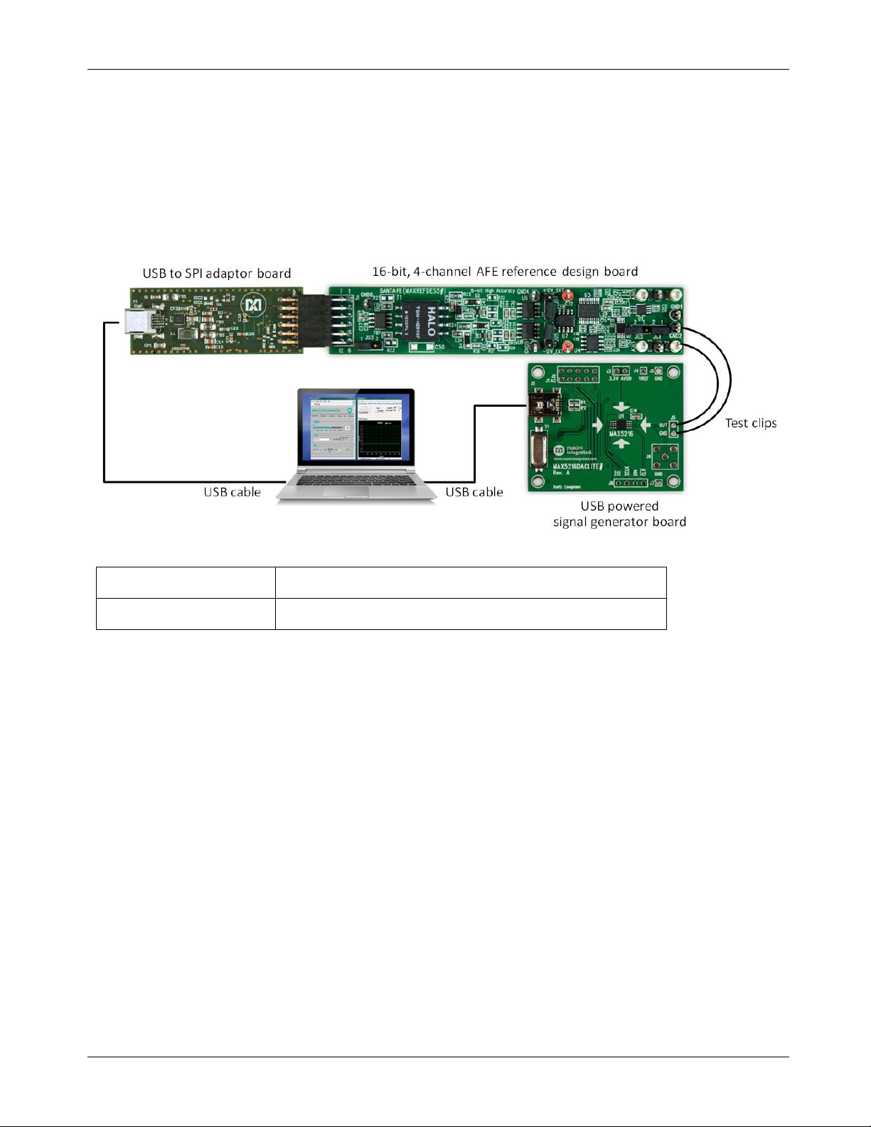
1 Introduction
The MAXSANTAFEEVSYS kit allows users to quickly demonstrate and evaluate the functionality of the
MAXREFDES5 4-channel analog front-end (AFE) reference des ig n without the need for a benc h po wer supp l y,
signal generator equipm ent, or Xilinx develo pment kit. The referenc e design board c onnects to a PC through
an included USB-to-SPI adaptor that pr ovides both power and data com munication to the board. To test the
AFE reference design, a USB-powered signal generator board utilizing one of Maxim’s digital-to-analog
converters (DACs) is als o included. Windows®-based graphical user i nterfaces (GUIs) comm unicate with the
boards for generating various analog signal test patterns and simplified access to AFE measurement data.
1.1 Ordering Information
PART DESCRIPTION
MAXSANTAFEEVSYS# Bundled kit for PC evaluation of MAXREFDES5 4-Ch AFE
#Denotes a RoHS-compliant device that may include lead that is exempt under the RoHS requirements.
1.2 Package Contents
The MAXSANTAFEEVSYS kit includes the following:
• MAXREFDES5 4-channel AFE board
• USB2PMB1 USB to Pmod
• MAX5216DACLITE signal generator board
• Two (2) wires with hook clips (1 red and 1 black)
• Two (2) USB type A male to USB type B mini cables
• USB flash drive with documentation, GUI applications, and USB Drivers
• Quick Start Guide (print copy)
TM
Type 2A adaptor board
1.3 System Requirements
The MAXSANTAFEEVSYS kit only requires use of a PC with the following:
• Minimum 1GHz processor and 1GB RAM
• Minimum 1024 x 768 video display resolution
• Two available USB ports
• Microsoft Windows 8, Windows 7, Windows Vista, or Windows XP®
Rev 0 3
Page 4
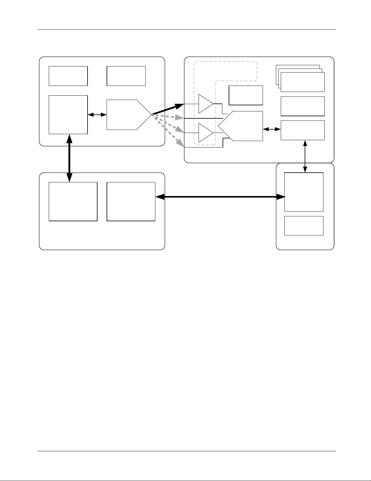
MAX1301
16-bit ADC
MAX5216
16-bit DAC
MAXQ622
Controller
MAX8510
LDO
MAX6133
VREF
OA
OA
MAX9632 OpAmps
(on 2 of 4-
Ch)
MAX14850
Dig. Isolator
MAX6126
VREF
MAX256
Xfmr Driver
MAX1659
LDO
FT2232HL
USB
Controller
MAX
1556
DC
/DC
PC with Windows 8, 7, Vista, or XP
USB
USB
MAX5216
DACLite GUI
Application
REFDES5
PMOD GUI
Application
MAX5216DACLITE
MAXREFDES5
USB2PMB1
1.4 Functional Diagram
MAXSANTAFEEVSYS User Manual
Rev 0 4
Page 5

MAXSANTAFEEVSYS User Manual
2 Software Installation
There are two Windows GUI applications included with MAXSANTAFEEVSYS used for:
• Generating analog test sign als with t he M AX 521 6D AC LITE board in order to eval uate th e per f or mance
of the AFE reference design. This application is create d using Nat ional Instruments LabVIEW
LabVIEW Run-Time Engine (RTE) must be installed in order to install and execute the
MAX5216DACLITE GUI application.
• Calibrating the offs et and gain for the analog inputs of the MAXREFDES5 boar d and evaluating the
design’s measurem ent perform ance. This applicat ion created us ing Borland C ++ does n ot require any
installation and can be executed directly from the USB flash drive.
To begin software ins tallation, either connect th e provided USB flash dri ve to an availab le USB port on your
PC, or download a zip file of the USB flash drive contents from
www.maximintegrated.com/MAXSANTAFEEVSYS
Administrator privileges are required for installing the provided software.
and extract to a location on your local hard drive.
®
. The NI
2.1 MAX5216DACLite Signal Generator Software Installation
Although the Setup.exe fi le located in the \DACLITE\ dir ector y includes t he LabV IEW RTE, it is rec omm ended
to f ollow the instructions below for best resu lts across diff erent Windows operat ing systems and us er account
types.
1. Browse to the \DACLITE\ directory found o n the USB f lash drive or in the extracted dir ectory from the
downloaded zip file.
2. Run LVRTE_SETUP.exe t o install NI ’s 2012 (32-bit) Runtime Engine. Do NO T restart o r shut down
the PC after completion of this installation. Choose the R estart Later option when prompted and
proceed to step #3 below.
3. Run DACLITE_SETUP.exe after completion of step #2 above.
4. Restart the PC when prompted.
Rev 0 5
Page 6

MAXSANTAFEEVSYS User Manual
3 Connections
This section describes t he basic connections with the MAXSANTAFEEVSYS kit. Two available USB port s are
required for operating the MAXSANTAFEEVSYS kit setup. If needed, copy the \MAXREFDES5\ and
\USB2PMB1\ directories from the USB flash drive to your PC to free up a USB port.
All boards derive power f rom the USB ports. The USB2PM B1 board includes on-board DC-DC conversion for
providing 3.3V DC to the MAXREFDES5 AFE board (or any other 3.3V Pmod Type 2A board). To provide
external power to th e MAXREFDES5 board, refer to Application Note 5561 included in the \MAXREFDES5\
directory and located at www.maximintegrated.com/AN5561
(Pmod™) form factor, refer to the Digilent PmodTM Interface Specification or visit www.DigilentInc.com.
3.1 MAX5216DACLITE Signal Generator Board
Connect one of the provided USB cables between the MAX5216DACLITE board and PC. The on-board
controller presents itself to the PC as a USB HID class device in the Windows Device Manager as shown
below and does not require any third-party drivers.
. For more inf orm ation on the Perip hera l Module
3.2 USB2PMB1 USB Adaptor Board
Connect the other provided USB cable between the USB2PMB1 board and PC. The USB2PMB1 adaptor
board includes an FTDI FT2232HL US B controller IC that perfor ms the USB functions and conv ersion to SPI.
Upon attaching the USB2PMB1 adaptor board to the PC, the Found New Hardware Wizard automatically
launches and installs the appropriate driver f iles if already located on your PC. If your PC does not find the
FTDI driver files on its local hard disk drive, locate and reference the \USB2PMB1\CDM v2.10.00 WHQL
Certified\ subdirectory to install FTDI’s D2XX driver.
Multiple drivers will be inst alled befor e it is read y to use. To verify proper ins tallation , one shoul d see two USB
Serial Converters (A and B) in the Device Manager as shown below.
Rev 0 6
Page 7

MAXSANTAFEEVSYS User Manual
J5
OUT
GND
VREF
J4
AIN0
GND0
AIN1
AIN3
GND3
AIN2
GND2
GND1
JU2 JU1
MAXREFDES5
MAX5216DACLITE
AIN0
GND0
AIN1
AIN3
GND3
AIN2
GND2
GND1
JU2 JU1
J5
OUT
GND
VREF
J4
MAXREFDES5
MAX5216DACLITE
Input AIN0
Input AIN1
0V to +3V from DACLITE J5
0V to +3V from DACLITE J5
AIN0
GND0
AIN1
AIN3
GND3
AIN2
GND2
GND1
JU2 JU1
J5
OUT
GND
VREF
J4
MAXREFDES5
MAX5216DACLITE
AIN0
GND0
AIN1
AIN
3
GND3
AIN2
GND2
GND1
JU2 JU1
J5
OUT
GND
VREF
J4
MAXREFDES5
MAX5216DACLITE
Input AIN2
Input AIN3
+1V to +3V from DACLITE J5 with JU2 removed
0V to +3V from DACLITE J5
3.3 MAXREFDES5 4-Ch AFE Board
Connect the MAXREFDES 5 board to t he USB2 PMB1 adaptor. Both connectors shou ld be on the s am e side of
the PCB when mated together as shown below.
3.3.1 Analog Signal Connections
The following table summarizes the different connec tion options for the MAXSANTAF EEVSYS kit. Note t he
input range of the MAXREFDES5 analog inputs exceeds the output capabilities of the MAX5216DACLITE
board included with the kit.
For testing input AI N2 with a voltage source, a j umper JU2 should be removed to disconnect t he on-board
sense resistor. Jumper JU1 on AIN2 is provided for optional connection to a reference ammeter.
(or -10V to +10V from alternate source)
(or 4-20mA from current source with JU2 installed)
Rev 0 7
(or -10V to +10V from alternate source)
(or 0V to +10V from alternate source)
Page 8

MAXSANTAFEEVSYS User Manual
BOARD
INPUT
ADC INP UT
RANGE
MAX1301 INPUT
CONFIGURATION
C[2:0] = 011
FSR= 3 x V
REF
4 Graphical User Interfaces
Before launching the GUI applications, make sure the USB2PMB1 and MAX5216DACLITE boards are
connected to the PC as described in the previous section.
4.1 GUI for MAXREFDES5
With the USB2PMB1 board conn ected, run (double-click) the PMOD_SPI.exe GUI appl ication located in the
\MAXREFDES5\ directory. Once the window below ap pears, press the Connect PMOD button and verif y that
the button changes its text to Disconnect PMOD and the status bar at the bottom indicates that the
companion board is connected.
4.1.1 Input Selection and Configuration
While most of the controls in the GUI only adjust the display of information on the screen, there are two
controls that both adjust the G UI display and configur e the MAX1301 ADC devic e used in the MAXREFDES 5
design. These c ontrols send a comm and to the MAX1301 indicating which input to sam ple and the full scale
range (FSR) for that input. The recommended combinations for the MAXREFDES5 hardware design are
shown in the left t wo columns of the table below. F or reference, th e respective channel select bits C[2:0] and
range select bits R[2:0] are also provided along with the full-scale range.
AIN0
-10V to 10V
AIN1
-10V to 10V
AIN2
4mA to 20mA
AIN3
0V to 10V
-12V to +12V
-12V to +12V
0V to +6V
0V to +12V
C[2:0] = 000
R[2:0] = 111
FSR= 6 x V
C[2:0] = 001
R[2:0] = 111
FSR= 6 x V
C[2:0] = 010
R[2:0] = 011
FSR= (3 x V
R[2:0] = 110
REF
REF
REF
) / 2
Rev 0 8
Page 9

MAXSANTAFEEVSYS User Manual
1 5 6 4 2
3
4.1.2 Sampling Controls
The GUI provides th e user with two options for th e sampling of data from the MAXREFDES5. The Sample
button captures a discrete number of samples as selected in the No. of Samples drop down menu and
displays the results. To start continuously collecting and displaying measurement data, press the Sample
Continuously button. When enabled, the butto n changes its text to Stop Sampling. In this mode, the No. of
Samples value determ ines the time base f or displayed res ults. For best GUI per formance, do not set th e No.
of Samples above 16384.
The Sample Rate drop down selection allows the user to choose the sample rate or the number of
conversions init iated by the GUI per second. The m ax allowable sample rate is determined by the MAX1301
device.
4.1.3 Results
The real-time scope on the left s ide of the GUI represents the m easured data with No. of Samples used for
the x-axis as described in the sec tion above. T his sec tion descr ibes t he res t of th e GUI disp la y controls, which
execute no control or command of the MAX1301 device.
1) Scope | Histogram: This tab a llows the user to choo se between the Scope plot with configurable xand y-axis or the Histogram plot with the ADC code on the x-axis and the num ber of occur rences o n
the y-axis.
2) Show History of average: Checking this optio n allows the user to v iew ent ire data in h istor y up to the
history length selected in the History Length drop-down menu.
3) Averaging: A Build average of drop-do wn menu is also pro vided for the num ber of disc rete sam ples
to average for each displayed data point.
Rev 0 9
Page 10

MAXSANTAFEEVSYS User Manual
4) Plot View Options:
i. Plot Counts: This option plots the ADC code itself on the Y-axis with the number of samples
on the x-axis.
ii. Plot Volts: This option plots the converted Voltage value.
iii. Plot Current: Plots the current measured across the 250Ω shunt resistance on the AIN2 input.
iv. Plot Temp: Reserved for future use.
5) Scope Options: Holding the mouse cursor over the top right corner of the Scope or the Histogram plot
will display the plot settings options available to the user which includes Play/Pause, Zoom in/out, Pan,
Print, Save and waveform settings.
6) Plot i n Wi nd ows: This pushbutton allows user to view the following displays in separate windo ws:
I. ADC Code of the current reading
II. FFT measurement
III. Histogram Measurement
Rev 0 10
Page 11

MAXSANTAFEEVSYS User Manual
4.1.4 Calibration
For precision results, it is r ecommended to calibrat e the MAXREFDES5 hard ware using the function pr ovided
with the GUI. Calibration par ameters for each combination of input channel and input r ange are stored in a
local file in the GUI direct ory on the PC . Press the Calibration button to ope n a window with the calibration
parameters.
i. Save Settings to File: Saves the current settings to a local file on the PC. This should be done for
each valid combination of input channel and range (i.e. Input AIN0 with Input Range -12V to +12V).
ii. Offset: Offset calibrat ion is done by forcing a 0V input vo ltage or 0m A current at the ph ysical input.
The resulting plot counts value, if other than 0, should be entered in the offset digit tab of the
calibration window. Hit Tab on the keyboard for the value to be app li ed.
iii. Volt per Code: This optio n calibrates for gain er ror and should be adjus ted after offset calibrati on.
The volt-per-code c alibration is done by forci ng a lar ger m agnitude voltage a t the i nput to obtain t he
code. W ith the MAX5216D ACLITE generator , this is lim ited to +3V (for best results with the max 3V
output, m ove the jum per wire f rom OUT of J5 to VREF of J4). Hit Tab on the k eyboard f or the valu e
to be applied.
Volt per code =
iv. Read Settings from File: Reads the last set tin gs th at ar e i n t he f il e and returns the user to the input
and calibration values from the last sav ed settings. If one wishes to res et to fac tory default, t hen the
appropriate .ini file has to be deleted.
v. Shunt Resistor value: This option stores the exact value of shunt resistance of the board. This
optional field allows the user to change the resistance and scale the current measured.
Example Calibration Sequence:
STEP DESCRIPTION CONNECTIONS DACLITE GUI REFDES5 GUI
1 AIN0 Offset Cal
2 AIN0 Gain Cal Single Operation: 2.5V
3 Save Settings -- -4 AIN1 Offset Cal
5 AIN1 Gain Cal Single Operation: 2.5V
6 Save Settings -- -7 AIN2 Offset Cal
8 AIN2 Gain Cal Single Operation: 2.5V
9 Save Settings -- -10 AIN3 Offset Cal
11 AIN3 Gain Cal Single Operation: 2.5V
12 Save Settings -- --
J5:OUT to AIN0
J5:GND to GND0
J5:OUT to AIN1
J5:GND to GND1
J5:OUT to AIN2
J5:GND to GND2
J5:OUT to AIN3
J5:GND to GND3
Single Operation: 0V
Single Operation: 0V
Single Operation: 0V
Single Operation: 0V
AIN0 with -12V to +12V
Input Range Selected
AIN1 with -12V to +12V
Input Range Selected
AIN2 with 0V to +6V
Input Range Selected
AIN3 with 0V to +12V
Input Range Selected
Rev 0 11
Page 12

MAXSANTAFEEVSYS User Manual
4.2 GUI for MAX5216DACLITE
With the MAX5216DACLITE board connected, click on the MAX5216DACLite shortcut found in the Start
menu. The GUI will automatica lly connect to the MAX5216 DACLITE hardware u pon initialization. T his section
describes the basic func tionalit y needed to generate t est signa ls for evaluating the MAX REFDES5 des ign. For
more information on the MAX5216DACLITE GUI, refer to the MAX5216DACLITE data sheet
information on the MAX5216 or other evaluation kits for the MAX5216, visit
www.maximintegrated.com/MAX5216.
. For more
The Single Operation tab sheet is active by default. The application checks all the compatible boards
connected to the PC a nd indic ates them on the right side of the GUI (up to 16 bo ards can be c onnec ted). An y
possible operation c an be eva lu ated on th e Sin gl e Operation tab sheet. For example, move the track bar slider
to set the DAC output voltage. The DAC Control sp in box reflects the slider po sition with a decimal number.
The DAC output c an also be s et b y t yping in a dec im al, hexadec im al, or an octa l or binar y va lue dir ectl y in t he
DAC Control spin box. The MAX5216 ac cepts codes from 0 to 65535 (21 6-1) decim al or from 0 to FFFF hex.
The notation is displayed on the left side of the box and can be changed by clicking on the notation character.
The Rising Ram p, Falling Ramp, Triangle, Sine, Square wave, or Staircase tab sheets gi ve the DAC the
ability to generate diff erent waveform s with the selected parameters. There is a possible delay to start a new
waveform until the pr evious one finish es a f ull c ycle when s witchin g bet ween tabs. To stop or start runnin g the
signal generator application, use the toolbar at the top of the application window.
Rev 0 12
Page 13

MAXSANTAFEEVSYS User Manual
Application Note 5561
PCB Source Files
Schematics (PDF)
Layout (Gerber)
5 Hardware Description
This section provides more information on the hardware design of the thr ee boar d s inc lud ing schematics, bill of
materials, and PCB layout files.
5.1 MAXREFDES5
The MAXREFDES5 r eference design is a 4-channel ana log front-end (AFE) that ac cepts -10V to +10V, 0 to
10V, and 4–20mA cur rent loop sig nals. T he des ign integr ates a 16-bit ADC with inno vative on-c hip att enuati on
(MAX1301) plus low-noise high-impedance an alog buffers (MAX9632) on two of the input chan nels and an
ultra-high precision 4.096V voltage reference (MAX6 126) to achieve maximum performance from the 16-bit
system. A 600V
isolated data and power connections to the host system . LDO regulators (MAX 1659) provide reg ulated +12V,
-12V, and 5V power rails to the analog front-end.
Application Note 5561 (REFD5561)
MAXREFDES5 referenc e des ign. Below is a summ ar y of the other hardware desi gn files available on the USB
flash drive. Application Note 5561 contains the latest links to hardware design Files.
5.2 MAX5216DACLITE
digi tal isolator (MAX14850) and 3 W transformer driver (M AX256) provide the necessar y
RMS
pro vides more inform ation on the design and perf ormance results of the
USB Flash Drive
Bill of Materials
Layout (PDF)
The MAX5216DACLite board utilizes a low power 16-bit DAC (MAX5216) with a precise 3.000V voltage
reference (MAX6133) that provides a low noise and low dropout reference for the DAC. The MAX5216
receives commands from the 16-bit MAXQ622 microcontroller through a 3-wire high-speed SPI bus. The
MAX5216 can run at 50M Hz clock frequency, but the SP I bus speed is limited to 6MH z on this board by the
microcontroller. T he devices are powered by a MAX8510 lo w-noise voltage regulator, which gets power from
the USB port and produces a fixed VDD level of 3.3V.
The above limitations are reflected by the suf fix “Lite” in the nam e of the board. For m ore information on the
MAX5216DACLITE (including board modifications), refer to the MAX5216DACLITE data sheet
information on the MAX5216 or other evaluation kits for the MAX5216, go to:
www.maximintegrated.com/MAX5216.
. For more
5.3 USB2PMB1
The USB2PMB1 board us es the FT2232HL, a USB 2.0 H igh Speed (480Mb/s) to UART /FIFO IC, to process
commands sent by a GUI application running on the PC. The design integrates a 4K MICROWIRE®compatible serial EEPROM (93LC66BT) and a low-power, 1.2A, PWM step-down DC-DC converter
(MAX1556) for generating 3.3V (VCCIO) from the 5V USB supply. VCCIO provides power to the FTDI chip, the
4k MICROWIRE EEPROM, and to the 12-pin connector for 3.3V Pmod Type 2A compatible boards.
For more information on the USB2PMB1 hardware design or other compatible boards from Maxim, go to
www.maximintegrated.com/USB2PMB1
factor, refer to the D igile nt PmodTM Interface Specification or visit www.DigilentInc.com.
. For more information on the Peripheral Module (Pmod™) form
Rev 0 13
Page 14

MAXSANTAFEEVSYS User Manual
6 Contact Information
For more information about Maxim Integrated products, contact technical support at
www.maximintegrated.com/support
.
7 Trademarks
LabVIEW is a registered trademark of National Instruments Corp.
MICROWIRE is a registered trademark of National Semiconductor Corp.
Pmod is a trademark Digilent Inc.
Windows is a registered trademark and registered service mark and Windows XP is a registered trademark of
Microsoft Corporation.
Rev 0 14
Page 15

MAXSANTAFEEVSYS User Manual
NUMBER
DATE
—
8 Revision Histor y
REVISION
0 5/14 Initial release
REVISION
DESCRIPTION
PAGES
CHANGED
Rev 0 15
 Loading...