

Page 1
For pricing, delivery, and
ordering information, please contact Maxim Direct
at 1-888-629-4642, or visit Maxim’s website at www.maximintegrated.com.
MAXQ FAMILY USER’S GUIDE
Data
Memory
I/O
Source
IR
1:16 16:1
Instruction
Decoder
IP
DP
SP
ALU
I/O
I/O
Program
Memory
Destination
Note: The MAXQ Family User's Guide should be used in conjunction with the data sheet(s) for MAXQ microcontrollers.
Rev: 6; 9/08
Page 2

MAXQ Family User’s Guide
TABLE OF CONTENTS
SECTION 1: Overview . . . . . . . . . . . . . . . . . . . . . . . . . . . . . . . . . . . . . . . . . . . . . . . . . . . . . . . . . . . .1-1
SECTION 2: Architecture . . . . . . . . . . . . . . . . . . . . . . . . . . . . . . . . . . . . . . . . . . . . . . . . . . . . . . . . . .2-1
SECTION 3: Programming . . . . . . . . . . . . . . . . . . . . . . . . . . . . . . . . . . . . . . . . . . . . . . . . . . . . . . . . .3-1
SECTION 4: System Register Descriptions . . . . . . . . . . . . . . . . . . . . . . . . . . . . . . . . . . . . . . . . . . . .4-1
SECTION 5: Peripheral Register Modules . . . . . . . . . . . . . . . . . . . . . . . . . . . . . . . . . . . . . . . . . . . . .5-1
SECTION 6: General-Purpose I/O Module . . . . . . . . . . . . . . . . . . . . . . . . . . . . . . . . . . . . . . . . . . . .6-1
SECTION 7: Timer/Counter Timer . . . . . . . . . . . . . . . . . . . . . . . . . . . . . . . . . . . . . . . . . . . . . . . . . . .7-1
SECTION 8: Timer/Counter 1 Module . . . . . . . . . . . . . . . . . . . . . . . . . . . . . . . . . . . . . . . . . . . . . . . .8-1
SECTION 9: Timer/Counter 2 Module . . . . . . . . . . . . . . . . . . . . . . . . . . . . . . . . . . . . . . . . . . . . . . . .9-1
SECTION 10: Serial I/O Module . . . . . . . . . . . . . . . . . . . . . . . . . . . . . . . . . . . . . . . . . . . . . . . . . . . .10-1
SECTION 11: Serial Peripheral Interface (SPI Module) . . . . . . . . . . . . . . . . . . . . . . . . . . . . . . . . . .11-1
SECTION 12: Hardware Multiplier Mode . . . . . . . . . . . . . . . . . . . . . . . . . . . . . . . . . . . . . . . . . . . . .12-1
SECTION 13: 1-Wire Bus Master . . . . . . . . . . . . . . . . . . . . . . . . . . . . . . . . . . . . . . . . . . . . . . . . . . .13-1
SECTION 14: Real-Time Clock Module . . . . . . . . . . . . . . . . . . . . . . . . . . . . . . . . . . . . . . . . . . . . . .14-1
SECTION 15: Test Access Port (TAP) . . . . . . . . . . . . . . . . . . . . . . . . . . . . . . . . . . . . . . . . . . . . . . .15-1
SECTION 16: In-Circuit Debug Mode . . . . . . . . . . . . . . . . . . . . . . . . . . . . . . . . . . . . . . . . . . . . . . .16-1
SECTION 17: In-System Programming (JTAG) . . . . . . . . . . . . . . . . . . . . . . . . . . . . . . . . . . . . . . . .17-1
SECTION 18: MAXQ Family Instruction Set Summary . . . . . . . . . . . . . . . . . . . . . . . . . . . . . . . . . .18-1
REVISION HISTORY . . . . . . . . . . . . . . . . . . . . . . . . . . . . . . . . . . . . . . . . . . . . . . . . . . . . . . . . . . . .Rev-1
Maxim Integrated
2
Page 3

MAXQ Family User’s Guide
SECTION 1: OVERVIEW
This section contains the following information:
1.1 Instruction Set . . . . . . . . . . . . . . . . . . . . . . . . . . . . . . . . . . . . . . . . . . . . . . . . . . . . . . . . . . . . . .1-2
1.2 Harvard Memory Architecture . . . . . . . . . . . . . . . . . . . . . . . . . . . . . . . . . . . . . . . . . . . . . . . . .1-2
1.3 Register Set . . . . . . . . . . . . . . . . . . . . . . . . . . . . . . . . . . . . . . . . . . . . . . . . . . . . . . . . . . . . . . .1-2
1.4 MAXQ10 and MAXQ20 Microcontrollers . . . . . . . . . . . . . . . . . . . . . . . . . . . . . . . . . . . . . . . . .1-3
1-1
Maxim Integrated
Page 4

MAXQ Family User’s Guide
SECTION 1: OVERVIEW
The MAXQ®family of 16-bit reduced instruction set computing (RISC) microcontrollers is targeted toward low-cost, low-power, embedded-application designs. The flexible, modular architecture design used in these microcontrollers allows development of targeted
designs for specific applications with minimal effort.
Microcontrollers in the MAXQ family provide many different combinations of program memory, data memory, and peripherals while supporting a common feature set. This shared functionality provides maximum reusability for hardware and software systems developed
using these microcontrollers.
1.1 Instruction Set
All MAXQ microcontrollers share a common instruction set, with all instructions a fixed 16 bits in length. A register-based, transporttriggered architecture allows all instructions to be coded as simple transfer operations. All instructions reduce to either writing an immediate value to a destination register or memory location or moving data between registers and/or memory locations.
This simple top-level instruction decoding allows all instructions to be executed in a single cycle. Since all CPU operations are performed on registers only, any new functionality can be added by simply adding new register modules. The simple instruction set also
provides maximum flexibility for code optimization by a compiler.
1.2 Harvard Memory Architecture
Program memory, data memory, and register space on MAXQ microcontrollers are separate from one another, and are each accessed
by a separate bus. This type of memory architecture (known as a Harvard architecture) has some advantages.
First, the word lengths can be different for different types of memory. Program memory must be 16 bits wide to accommodate the
instruction word size, but system and peripheral registers can be 8 bits wide or 16 bits wide as needed. Since data memory is not
required to store program code, its width may also vary and could conceivably be targeted for a specific application.
Also, since data memory is accessed by the CPU only through appropriate registers, it is possible for register modules to access memory entirely independent from the main processor, providing the framework for direct memory-access operations. It is also possible to
have more than one type of data memory, each accessed through a different register set.
1.3 Register Set
Since all functions in the MAXQ family are accessed through registers, common functionality is provided through a common register
set. Many of these registers provide the equivalent of higher level op codes by directly accessing the arithmetic logic unit (ALU), the
loop counter registers, and the data pointer registers. Others, such as the interrupt registers, provide common control and configuration functions that are equivalent across all MAXQ microcontrollers.
The common register set, also known as the System Registers, includes the following:
• ALU access and control registers, including working accumulator registers and the processor status flags
• Two Data Pointers and a Frame Pointer for data memory access
• Auto-decrementing Loop Counters for fast, compact looping
• Instruction Pointer and other branching control access points
• Stack Pointer and an access point to the 16-bit-wide dedicated hardware stack
• Interrupt vector, identification, and masking registers
Peripherals and other features that can vary among MAXQ microcontroller devices are accessed through Peripheral registers. These
registers, grouped into register modules, provide such additional functionality as:
• Universal Asynchronous Receiver/Transmitter (UART) Serial Ports
• High-Speed Timers and Counters
• Serial Peripheral Interface (SPI™) ports
• Hardware Multiplier
MAXQ is a registered trademark of Maxim Integrated Products, Inc.
SPI is a trademark of Motorola, Inc.
Maxim Integrated
1-2
Page 5

MAXQ Family User’s Guide
• Real-Time Clock
• 1-Wire® Bus Master
• General-Purpose Digital I/O Ports
1.4 MAXQ10 and MAXQ20 Microcontrollers
This user’s guide covers both the 8-bit MAXQ10 and 16-bit MAXQ20 microcontrollers. The primary difference between the MAXQ10
and MAXQ20 implementations is the width of the internal data bus and ALU. The MAXQ10 design implements an 8-bit internal data
bus and ALU, while the MAXQ20 design implements a 16-bit internal data bus and ALU. This difference is most evident when comparing the instruction set, and more specifically, those operations that involve the ALU and accumulators. The registers on the MAXQ10
and MAXQ20 can be either 8 bits or 16 bits wide.
1-Wire is a registered trademark of Dallas Semiconductor Corp.
1-3
Maxim Integrated
Page 6

MAXQ Family User’s Guide
SECTION 2: ARCHITECTURE
This section contains the following information:
2.1 Instruction Decoding . . . . . . . . . . . . . . . . . . . . . . . . . . . . . . . . . . . . . . . . . . . . . . . . . . . . . . . .2-4
2.2 Register Space . . . . . . . . . . . . . . . . . . . . . . . . . . . . . . . . . . . . . . . . . . . . . . . . . . . . . . . . . . . . .2-5
2.3 Memory Organization . . . . . . . . . . . . . . . . . . . . . . . . . . . . . . . . . . . . . . . . . . . . . . . . . . . . . . . .2-6
2.3.1 Program Memory . . . . . . . . . . . . . . . . . . . . . . . . . . . . . . . . . . . . . . . . . . . . . . . . . . . . . .2-6
2.3.2 Utility ROM . . . . . . . . . . . . . . . . . . . . . . . . . . . . . . . . . . . . . . . . . . . . . . . . . . . . . . . . . . .2-6
2.3.3 Data Memory . . . . . . . . . . . . . . . . . . . . . . . . . . . . . . . . . . . . . . . . . . . . . . . . . . . . . . . . .2-6
2.3.4 Stack Memory . . . . . . . . . . . . . . . . . . . . . . . . . . . . . . . . . . . . . . . . . . . . . . . . . . . . . . . . .2-7
2.4 Pseudo-Von Neumann Memory Mapping . . . . . . . . . . . . . . . . . . . . . . . . . . . . . . . . . . . . . . . .2-7
2.5 Pseudo-Von Neumann Memory Access . . . . . . . . . . . . . . . . . . . . . . . . . . . . . . . . . . . . . . . . .2-9
2.6 Data Alignment . . . . . . . . . . . . . . . . . . . . . . . . . . . . . . . . . . . . . . . . . . . . . . . . . . . . . . . . . . . . .2-10
2.6.1 Memory Management Unit . . . . . . . . . . . . . . . . . . . . . . . . . . . . . . . . . . . . . . . . . . . . . . .2-10
2.7 Clock Generation . . . . . . . . . . . . . . . . . . . . . . . . . . . . . . . . . . . . . . . . . . . . . . . . . . . . . . . . . . .2-13
2.7.1 Internal Ring Oscillator . . . . . . . . . . . . . . . . . . . . . . . . . . . . . . . . . . . . . . . . . . . . . . . . . .2-14
2.7.2 External Clock (Crystal/Resonator) . . . . . . . . . . . . . . . . . . . . . . . . . . . . . . . . . . . . . . . . .2-14
2.7.3 External Clock (Direct Input) . . . . . . . . . . . . . . . . . . . . . . . . . . . . . . . . . . . . . . . . . . . . . .2-14
2.7.4 External RC . . . . . . . . . . . . . . . . . . . . . . . . . . . . . . . . . . . . . . . . . . . . . . . . . . . . . . . . . .2-15
2.7.5 Internal System Clock Generation . . . . . . . . . . . . . . . . . . . . . . . . . . . . . . . . . . . . . . . . .2-15
2.8 Interrupts . . . . . . . . . . . . . . . . . . . . . . . . . . . . . . . . . . . . . . . . . . . . . . . . . . . . . . . . . . . . . . . . .2-16
2.8.1 Servicing Interrupts . . . . . . . . . . . . . . . . . . . . . . . . . . . . . . . . . . . . . . . . . . . . . . . . . . . . .2-16
2.8.2 Interrupt System Operation . . . . . . . . . . . . . . . . . . . . . . . . . . . . . . . . . . . . . . . . . . . . . . .2-16
2.8.3 Synchronous vs. Asynchronous Interrupt Sources . . . . . . . . . . . . . . . . . . . . . . . . . . . . .2-17
2.8.4 Interrupt Prioritization by Software . . . . . . . . . . . . . . . . . . . . . . . . . . . . . . . . . . . . . . . . .2-18
2.8.5 Interrupt Exception Window . . . . . . . . . . . . . . . . . . . . . . . . . . . . . . . . . . . . . . . . . . . . . .2-18
2.9 Operating Modes . . . . . . . . . . . . . . . . . . . . . . . . . . . . . . . . . . . . . . . . . . . . . . . . . . . . . . . . . . .2-18
2.9.1 Reset Mode . . . . . . . . . . . . . . . . . . . . . . . . . . . . . . . . . . . . . . . . . . . . . . . . . . . . . . . . . . .2-18
2-1
2.9.1.1 Power-On/Brownout Reset . . . . . . . . . . . . . . . . . . . . . . . . . . . . . . . . . . . . . . . . .2-18
2.9.1.2 External Reset . . . . . . . . . . . . . . . . . . . . . . . . . . . . . . . . . . . . . . . . . . . . . . . . . . .2-19
2.9.1.3 Watchdog Timer Reset . . . . . . . . . . . . . . . . . . . . . . . . . . . . . . . . . . . . . . . . . . . .2-19
2.9.1.4 Internal System Reset . . . . . . . . . . . . . . . . . . . . . . . . . . . . . . . . . . . . . . . . . . . . .2-19
Maxim Integrated
Page 7

MAXQ Family User’s Guide
2.9.2 Power Management Mode . . . . . . . . . . . . . . . . . . . . . . . . . . . . . . . . . . . . . . . . . . . . . . .2-19
2.9.2.1 Switchback . . . . . . . . . . . . . . . . . . . . . . . . . . . . . . . . . . . . . . . . . . . . . . . . . . . . .2-20
2.9.3 Stop Mode . . . . . . . . . . . . . . . . . . . . . . . . . . . . . . . . . . . . . . . . . . . . . . . . . . . . . . . . . . . .2-20
LIST OF FIGURES
Figure 2-1. MAXQ Transport-Triggered Architecture . . . . . . . . . . . . . . . . . . . . . . . . . . . . . . . . . . .2-3
Figure 2-2. Instruction Word Format . . . . . . . . . . . . . . . . . . . . . . . . . . . . . . . . . . . . . . . . . . . . . . . .2-4
Figure 2-3. Pseudo Von Neumann Memory Map (MAXQ10 Default) . . . . . . . . . . . . . . . . . . . . . .2-8
Figure 2-4. Pseudo Von Neumann Memory Map (MAXQ20 Default) . . . . . . . . . . . . . . . . . . . . . .2-9
Figure 2-5. CDA Functions (Word Access Mode) . . . . . . . . . . . . . . . . . . . . . . . . . . . . . . . . . . . . .2-11
Figure 2-6. CDA Functions (Byte Access Mode) . . . . . . . . . . . . . . . . . . . . . . . . . . . . . . . . . . . . . .2-12
Figure 2-7. MAXQ Clock Sources . . . . . . . . . . . . . . . . . . . . . . . . . . . . . . . . . . . . . . . . . . . . . . . . .2-13
Figure 2-8. On-Chip Crystal Oscillator . . . . . . . . . . . . . . . . . . . . . . . . . . . . . . . . . . . . . . . . . . . . . .2-15
Figure 2-9. RC Relaxation Oscillator . . . . . . . . . . . . . . . . . . . . . . . . . . . . . . . . . . . . . . . . . . . . . . .2-15
Figure 2-10. MAXQ Interrupt Source Hierarchy Example . . . . . . . . . . . . . . . . . . . . . . . . . . . . . . .2-17
LIST OF TABLES
Table 2-1. Register-to-Register Transfer Operations . . . . . . . . . . . . . . . . . . . . . . . . . . . . . . . . . . .2-5
Table 2-2. System Clock Rate Control Settings . . . . . . . . . . . . . . . . . . . . . . . . . . . . . . . . . . . . . . .2-15
Maxim Integrated
2-2
Page 8
MAXQ Family User’s Guide
SYSTEM MODULES/
REGISTERS
PERIPHERAL MODULES/REGISTERS
DATA
MEMORY
dst
MAXQ PRODUCT SPECIFIC
MODULES
(MULTIPLY ACCUMULATE UNIT,
ADC, DAC, PWM, ETC.)
STACK
MEMORY
CKCN
WDCN
IC
ADDRESS
GENERATION
IP
SP
IC
LOOP COUNTERS
LC[η]
IIR
IMR
INTERRUPT
LOGIC
CLOCK CONTROL,
WATCHDOG TIMER
AND POWER MONITOR
BOOLEAN
VARIABLE
MANIPULATION
ACCUMULATORS
(16)
AP
APC
PSF
INSTRUCTION
DECODE
(SRC, DST TRANSPORT
DETERMINATION)
MUX
DATA POINTERS
DP[0], DP[1]
FP =
(BP + OFFS)
DPC
SC
MEMORY MANAGEMENT
UNIT (MMU)
PROGRAM
MEMORY
src
dst
src
GENERAL-
PURPOSE
I/O
TIMERS/
COUNTERS
UART
AND SPI
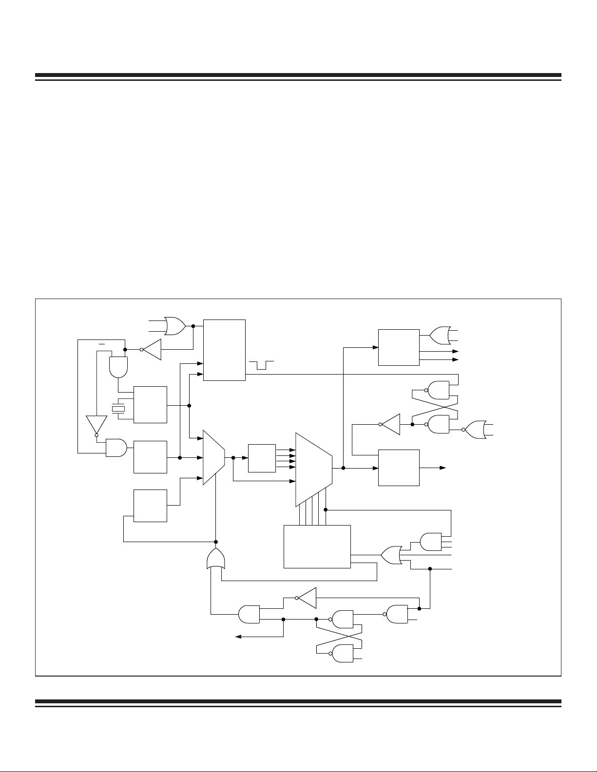
SECTION 2: ARCHITECTURE
The MAXQ architecture is designed to be modular and expandable. Top-level instruction decoding is extremely simple and based on
transfers to and from registers. The registers are organized into functional modules, which are in turn divided into the System Register
and Peripheral Register groups. Figure 2-1 illustrates the modular architecture and the basic transport possibilities.
Figure 2-1. MAXQ Transport-Triggered Architecture
2-3
Maxim Integrated
Page 9

MAXQ Family User’s Guide
FORMAT DESTINATION SOURCE
f
dddddddssssssss
Memory access from the MAXQ is based on a Harvard architecture with separate address spaces for program and data memory. The
simple instruction set and transport-triggered architecture allow the MAXQ to run in a nonpipelined execution mode where each instruction can be fetched from memory, decoded, and executed in a single clock cycle. Data memory is accessed through one of three data
pointer registers. Two of these data pointers, DP[0] and DP[1], are stand-alone 16-bit pointers. The third data pointer, FP, is composed
of a 16-bit base pointer (BP) and an 8-bit offset register (OFFS). All three pointers support post-increment/decrement functionality for
read operations and pre-increment/decrement for write operations. For the Frame Pointer (FP=BP[Offs]), the increment/decrement
operation is executed on the OFFS register and does not affect the base pointer (BP). Stack functionality is provided by dedicated
memory with a 16-bit width and a typical depth of 8 (although this varies dependent upon the MAXQ product). An on-chip memory
management unit (MMU) is accessible through system registers to allow logical remapping of physical program and data spaces, and
thus facilitates in-system programming and fast access to data tables, arrays, and constants physically located in program memory.
2.1 Instruction Decoding
Every MAXQ instruction is encoded as a single 16-bit word according to the format in Figure 2-2.
Figure 2-2. Instruction Word Format
Bit 15 (f) indicates the format for the source field of the instruction as follows:
• If f equals 0, the instruction is an immediate source instruction, and the source field represents an immediate 8-bit value.
• If f equals 1, the instruction is a register source instruction, and the source field represents the register that the source value will be
read from.
Bits 0 to 7 (ssssssss) represent the source for the transfer. Depending on the value of the format field, this can either be an immediate
value or a source register. If this field represents a register, the lower four bits contain the module specifier and the upper four bits contain the register index in that module.
Bits 8 to 14 (ddddddd) represent the destination for the transfer. This value always represents a destination register, with the lower four
bits containing the module specifier and the upper three bits containing the register sub-index within that module.
Since the source field is 8 bits wide and 4 bits are required to specify the module, any one of 16 registers in that module may be specified as a source. However, the destination field has one less bit, which means that only eight registers in a module can be specified
as a destination in a single-cycle instruction.
While the asymmetry between source and destination fields of the op code may initially be considered a limitation, this space can be
used effectively. Firstly, since read-only registers will never be specified as destinations, they can be placed in the second eight locations in a module to give single-cycle read access. Secondly, there are often critical control or configuration bits associated with system and certain peripheral modules where limited write access is beneficial (e.g., watchdog-timer enable and reset bits). By placing
such bits in one of the upper 24 registers of a module, this write protection is added in a way that is virtually transparent to the assembly source code. Anytime that it is necessary to directly select one of the upper 24 registers as a destination, the prefix register PFX is
used to supply the extra destination bits. This prefix register write is inserted automatically by the assembler and requires one additional execution cycle.
The MAXQ architecture is transport-triggered. This means that writing to or reading from certain register locations will also cause side
effects to occur. These side effects form the basis for the higher level op codes defined by the assembler, such as ADDC, OR, JUMP,
and so on. While these op codes are actually implemented as MOVE instructions between certain register locations, the encoding is
handled by the assembler and need not be a concern to the programmer. The registers defined in the System Register and Peripheral
Register maps operate as described in the documentation; the unused "empty" locations are the ones used for these special cases.
The MAXQ instruction set is designed to be highly orthogonal. All arithmetic and logical operations that use two registers can use any
register along with the accumulator. Data can be transferred between any two registers in a single instruction.
Maxim Integrated
2-4
Page 10

DESTINATION SET TO VALUE
SOURCE REGISTER SIZE
(BITS)
DESTINATION REGISTER
SIZE (BITS)
PREFIX SET?
HIGH 8 BITS LOW 8 BITS
88— Source [7:0]
8 16 No 00h Source [7:0]
8 16 Yes Prefix [7:0] Source [7:0]
16 8 — Source [7:0]
16 16 No Source [15:8] Source [7:0]
MAXQ Family User’s Guide
2.2 Register Space
The MAXQ architecture provides a total of 16 register modules. Each of these modules contains 32 registers. The first eight registers
in each module may be read from or written to in a single cycle; the second eight registers may be read from in a single cycle and written to in two cycles (by using the prefix register PFX); the last sixteen registers may be read or written in two cycles (always requiring
use of the prefix register PFX).
Registers may be either 8 or 16 bits in length. Within a register, any number of bits can be implemented; bits not implemented are fixed
at zero. Data transfers between registers of different sizes are handled as shown in Table 2-1.
• If the source and destination registers are both 8 bits wide, data is transferred bit to bit accordingly.
• If the source register is 8 bits wide and the destination register is 16 bits wide, the data from the source register is transferred into
the lower 8 bits of the destination register. The upper 8 bits of the destination register are set to the current value of the prefix register; this value is normally zero, but it can be set to a different value by the previous instruction if needed. The prefix register reverts
back to zero after one cycle, so this must be done by the instruction immediately before the one that will be using the value.
• If the source register is 16 bits wide and the destination register is 8 bits wide, the lower 8 bits of the source are transferred to the
destination register.
• If both registers are 16 bits wide, data is copied bit to bit.
Table 2-1. Register-to-Register Transfer Operations
The above rules apply to all data movements between defined registers. Data transfer to/from undefined register locations has the following behavior:
• If the destination is an undefined register, the MOVE is a dummy operation but may trigger an underlying operation according to the
source register (e.g., @DP[n]--).
• If the destination is a defined register and the source is undefined, the source data for the transfer will depend upon the source module
width. If the source is from a module containing 8-bit or 8-bit and 16-bit source registers, the source data will be equal to the prefix data
concatenated with 00h. If the source is from a module containing only 16-bit source registers, 0000h source data is used for the transfer.
The 16 available register modules are broken up into two different groups. The low six modules (specifiers 0h through 5h) are known
as the Peripheral Register modules, while the high 10 modules (specifiers 6h to Fh) are known as the System Register modules. These
groupings are descriptive only, as there is no difference between accessing the two register groups from a programming perspective.
The System Registers define basic functionality that remains the same across all products based on the MAXQ architecture. This
includes all register locations that are used to implement higher level op codes as well as the following common system features.
• ALU (MAXQ10: 8 bit; MAXQ20: 16 bit) and associated status flags (zero, equals, carry, sign, overflow)
• Eight working accumulator registers (MAXQ10: 8 bit width; MAXQ20: 16 bit width), along with associated control registers
• Instruction pointer
• Registers for interrupt control, handling, and identification
• Auto-decrementing Loop Counters for fast, compact looping
• Two Data Pointer registers and a Frame Pointer for data memory access
The Peripheral Registers define additional functionality that may be included by different products based on the MAXQ architecture. This
functionality is broken up into discrete modules so that only the features that are required for a given product need to be included. Since
the Peripheral Registers add functionality outside of the common MAXQ system architecture, they are not used to implement op codes.
2-5
Maxim Integrated
Page 11

MAXQ Family User’s Guide
2.3 Memory Organization
Beyond the internal register space, memory on the MAXQ microcontroller is organized according to a Harvard architecture, with a separate address space and bus for program memory and data memory. Stack memory is also separate and is accessed through a dedicated register set.
To provide additional memory map flexibility, an MMU allows data memory space to be mapped into a predefined program memory
segment, thus affording the possibility of code execution from data memory. Additionally, program memory space can be made accessible as data space, allowing access to constant data stored in program memory.
2.3.1 Program Memory
Program memory begins at address x0000h and is contiguous through the internal program memory. The actual size of the on-chip
program memory available for user application is product dependent. Given a 16-bit program address bus, the maximum program
space is 64kWords. Since the codewords are 16 bits, the program memory is therefore a 64k x 16 linear space.
Program memory is accessed directly by the program fetching unit and is addressed by the Instruction Pointer register. From an implementation perspective, system interrupts and branching instructions simply change the contents of the Instruction Pointer and force
the op code fetch from a new program location. The Instruction Pointer is direct read/write accessible by the user software; write access
to the Instruction Pointer will force program flow to the new address on the next cycle following the write. The content of the Instruction
Pointer will be incremented by 1 automatically after each fetch operation. The Instruction Pointer defaults to 8000h, which is the starting address of the utility ROM. The default IP setting of 8000h is assigned to allow initial in-system programming to be accomplished
with utility ROM code assistance. The utility ROM code interrogates a specific register bit in order to decide whether to execute in-system programming or jump immediately to user code starting at 0000h. The user code reset vector should always be stored in the lowest bytes of the program memory.
The program memory is normally implemented using nonvolatile memory, e.g., ROM, EEPROM, or Flash. ROM memory technology
requires program code to be masked into the ROM during chip fabrication; no write access to program memory is available. EEPROM
and Flash provide in-system programming capability but both technologies require that the memory targeted for the write operation be
unprogrammed (erased). The utility ROM provides routines to carry out the necessary operations (erase, write, verify) on these nonvolatile memories.
2.3.2 Utility ROM
A utility ROM is normally placed in the upper 32kWord program memory space starting at address 8000h. This utility ROM potentially
provides the following system utility functions:
• Reset vector
• Bootstrap function for system initialization
• In-application programming
• In-circuit debug
Following each reset, the processor automatically starts execution at address 8000h in the utility ROM, allowing ROM code to perform
any necessary system support functions. Next, the System Programming Enable (SPE) bit is examined to determine whether system
programming should commence or whether that code should be bypassed, instead forcing execution to vector to the start of user program code. When the SPE bit is set to logic 1, the processor will execute the prescribed Bootstrap Loader mode program that resides
in utility ROM. The SPE bit defaults to 0. To enter the Bootstrap Loader mode, the SPE bit can be set to 1 during reset via the JTAG
interface. When in-system programming is complete, the Bootstrap Loader can clear the SPE bit and reset the device such that the insystem programming routine is subsequently bypassed.
2.3.3 Data Memory
On-chip data memory begins at address x0000h and is contiguous through the internal data memory. The actual size of the on-chip
data memory available for the user application is product dependent. Data memory is accessed via indirect register addressing
through a Data Pointer (@DP[n]) or Frame Pointer (@BP[Offs]). The Data Pointer is used as one of the operands in a MOVE instruction.
If the Data Pointer is used as source, the core performs a Load operation that reads data from the data memory location addressed
by the Data Pointer. If the Data Pointer is used as destination, the core executes a Store operation that writes data to the data memory location addressed by the Data Pointer. The Data Pointer can be directly accessed by the user software.
The core incorporates two 16-bit Data Pointers (DP[0] and DP[1]) to support data memory accessing. All Data Pointers support indirect addressing mode and indirect addressing with auto-increment or auto-decrement. Data Pointers DP[0] and DP[1] can be used as
Maxim Integrated
2-6
Page 12

MAXQ Family User’s Guide
post increment/decrement source pointers by a MOVE instruction or pre increment/decrement destination pointers by a MOVE instruction. Using Data Pointer indirectly with "++" will automatically increase the content of the active Data Pointer by 1 immediately following the execution of read data transfer (@DP[n]++) or immediately preceding the execution of a write operation (@++DP[n]). Using
Data Pointer indirectly with "--" will decrease the content of the active Data Pointer by 1 immediately following the execution of read
data transfer (@DP[n]--) or immediately preceding the execution of a write operation (@--DP[n]).
The Frame Pointer (BP[Offs]) is formed by 16-bit unsigned addition of Frame Pointer Base Register (BP) and Frame Pointer Offset Register
(Offs). Frame Pointer can be used as a post increment/decrement source pointer by a MOVE instruction or as a pre increment/decrement
destination pointer. Using Frame Pointer indirectly with "++" (@BP[++Offs] for a write or @BP[Offs++] for a read) will automatically increase
the content of the Frame Pointer Offset by 1 immediately before or after the execution of data transfer depending upon whether it is used
as a destination or source pointer respectively. Using Frame Pointer indirectly with "--" (@BP[--Offs] for a write or @BP[Offs--] for a read)
will decrease the content of the Frame Pointer Offset by 1 immediately before/after execution of data transfer depending upon whether it
is used as a destination or source pointer respectively. Note that the increment/decrement function affects the content of the Offs register
only, while the contents of the BP register remain unaffected by the borrow/carry out from the Offs register.
A data memory cycle contains only one system clock period to support fast internal execution. This allows read or write operations on
SRAM to be completed in one clock cycle. Data memory mapping and access control are handled by the MMU. Read/write access to
the data memory can be in word or in byte.
2.3.4 Stack Memory
A 16-bit wide on-chip stack is provided by the MAXQ for storage of program return addresses and general-purpose use. The stack is
used automatically by the processor when the CALL, RET, and RETI instructions are executed and when an interrupt is serviced; it can
also be used explicitly to store and retrieve data by using the @SP- - source, @++SP destination, or the PUSH, POP, and POPI instructions. The POPI instruction acts identically to the POP instruction except that it additionally clears the INS bit.
The width of the stack is 16 bits to accommodate the instruction pointer size. The stack depth may vary between product implementations. As the stack pointer register SP is used to hold the index of the top of the stack, the maximum size of the stack allowed for a
MAXQ product is defined by the number of bits defined in the SP register (e.g., 3 bits for stack depth of 8, 4 bits for stack depth of 16).
On reset, the stack pointer SP initializes to the top of the stack (e.g. 07h for an 8-word stack, 0Fh for a 16-word stack). The CALL, PUSH,
and interrupt vectoring operations increment SP and then store a value at @SP. The RET, RETI, POP, and POPI operations retrieve the
value at @SP and then decrement SP.
As with the other RAM-based modules, the stack memory is initialized to indeterminate values upon reset or power-up. Stack memory
is dedicated for stack operations only and cannot be accessed through program or data address spaces.
2.4 Pseudo-Von Neumann Memory Mapping
The MAXQ supports a pseudo-Von Neumann memory structure that can merge program and data into a linear memory map. This is
accomplished by mapping the data memory into the program space or mapping program memory segment into the data space.
Program memory from x0000h to x7FFFh is the normal user code segment, followed by the utility ROM segment. The uppermost part
of the 64kWord memory is the logical area for data memory when accessed as a code segment.
The program memory is logically divided into four program pages:
• P0 contains the lower 16kWords,
• P1 contains the second 16kWords,
• P2 contains the third 16kWords, and
• P3 contains the fourth 16kWords.
By default, P2 and P3 are not accessible for program execution until they are explicitly activated by the user software. The Upper
Program Access (UPA) bit must be set to logic 1 to activate P2 and P3. Once UPA is set, P2 and P3 will occupy the upper half of the
64kWord program space. In this configuration (UPA = 1), the utility ROM cannot be accessed at program memory and the physical
data memory cannot be accessed logically in program space.
The logical mapping of physical program memory page(s) into data space depends upon two factors: physical memory currently in
use for program execution; and word/byte data memory access selection. If execution is from the utility ROM, physical program memory page(s) can logically be mapped to the upper half of data memory space. If logical data memory is used for execution, physical
program memory page(s) can logically be mapped to the lower half of data memory space. If byte access mode is selected, only one
2-7
Maxim Integrated
Page 13
MAXQ Family User’s Guide
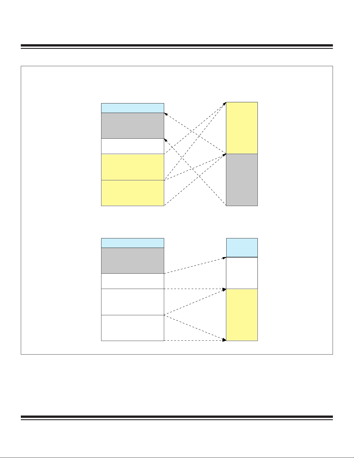
CDA1:0
SELECTED PAGE IN BYTE MODE
SELECTED PAGE IN
WORD MODE
00 P0 P0 and P1
01 P1 P0 and P1
10 P2 P2 and P3
11 P3 P2 and P3
PHYSICAL PROGRAM
(P0)
UTILITY ROM
PHYSICAL DATA
x0000
x8000
xA000
xFFFF
x0000
x8000
xFFFF
DATA MEMORYPROGRAM MEMORY
15 0 07
LOGICAL SPACE
LOGICAL SPACE
MAXQ10 MEMORY MAP (DEFAULT CONDITION)
PHYSICAL PROGRAM
(P1)
page (16kWords) may be logically mapped, as just defined, to either the upper or lower half of data memory. If word access mode is
selected, two pages (32kWords total) may be logically mapped to data memory. To avoid memory overlapping in the byte access
mode, the physical data memory should be confined to the address range x0000h to x3FFFh in word mode. The selection of physical
memory page or pages to be logically mapped to data space is determined by the Code Access Bits (CDA1:0):
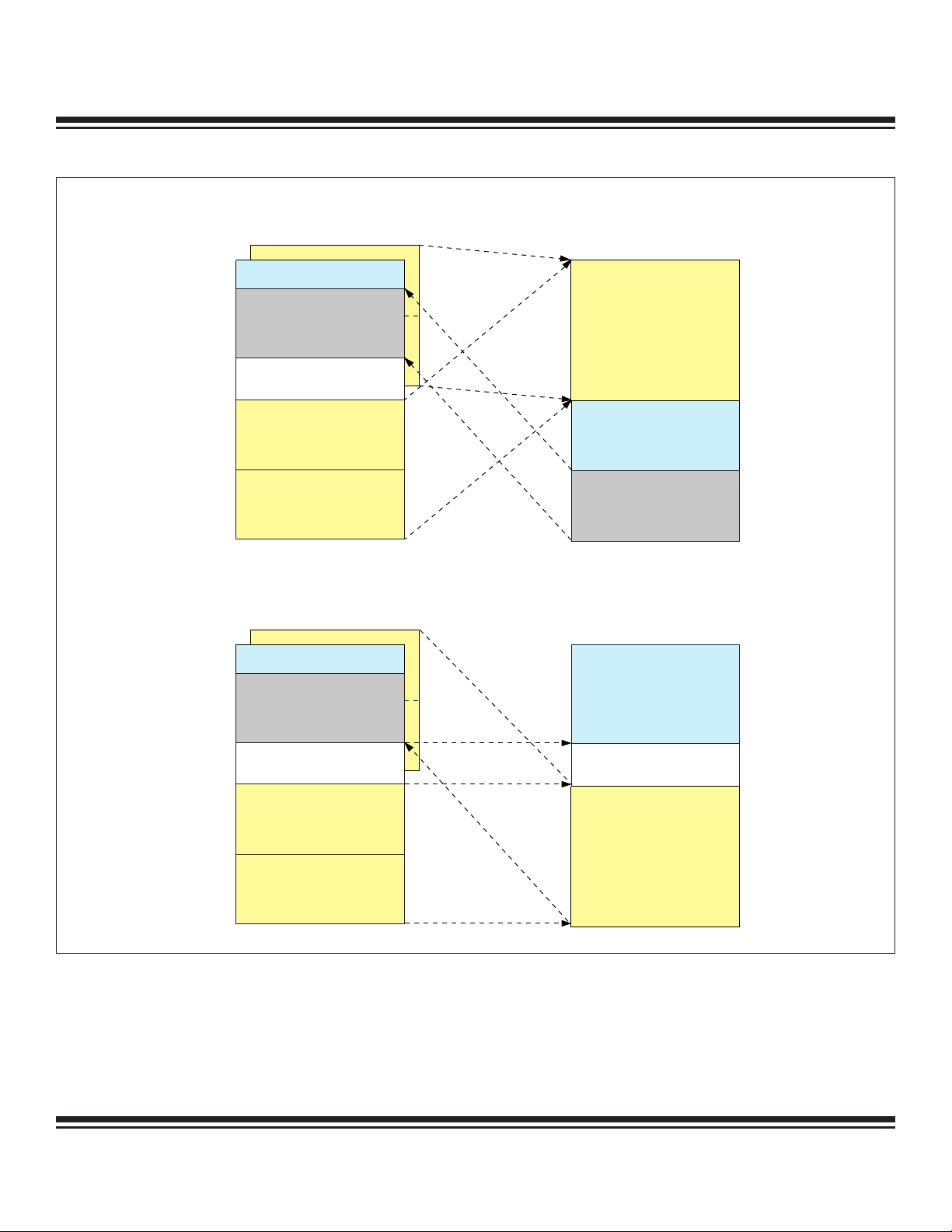
Figure 2-3 and Figure 2-4 summarize the default memory maps for this memory structure. The primary difference lies in the reset default
settings for the data pointer Word/Byte Mode Select (WBSn) bits. The WBSn bits of the MAXQ10 default to byte access mode (WBSn
= 0), while the MAXQ20 WBSn bits default to word access mode (WBSn = 1).
Figure 2-3. Pseudo Von Neumann Memory Map (MAXQ10 Default)
Maxim Integrated
2-8
Page 14
Physical Program
(P0)
PHYSICAL DATA
x0000
x8000
x4000
DATA MEMORY
0
15
LOGICAL SPACE
MAXQ20 MEMORY MAP (DEFAULT CONDITION, UPA = 0)
PHYSICAL DATA
x0000
x8000
xFFFF
x0000
x4000
x8000
DATA MEMORYPROGRAM MEMORY
15
0
0
15
LOGICAL SPACE
LOGICAL SPACE
MAXQ20 MEMORY MAP (UPA = 1, CDA IS DON’T CARE)
LOGICAL UTILITY ROM
P2
P3
PHYSICAL PROGRAM
(P3)
PHYSICAL PROGRAM
(P2)
PHYSICAL PROGRAM
(P1)
PHYSICAL PROGRAM
(P0)
xFFFF
xFFFF
PHYSICAL PROGRAM
(P0)
UTILITY ROM
x0000
x8000
xA000
xFFFF
PROGRAM MEMORY
15 0
LOGICAL SPACE
PHYSICAL PROGRAM
(P1)
MAXQ Family User’s Guide
Figure 2-4. Pseudo Von Neumann Memory Map (MAXQ20 Default)
2.5 Pseudo-Von Neumann Memory Access
The pseudo-Von Neumann memory mapping is straightforward if there is no memory overlapping among the program, utility ROM, and
data memory segments. However, for applications requiring large-size program memory, the paging scheme can be used to selectively
activate those overlapped memory segments. The UPA bit can be used to activate the upper half of the physical program code (P2 and
P3) for program execution. When accessing the program memory as data, the CDA bits can be used to select one of the four program
pages as needed. Full data memory access to any of the four physical program memory pages is based on the assumption that the maximum physical data memory is in the range of 16k x 16. The other restriction for accessing the pseudo-Von Neumann map is that when
program execution is in a particular memory segment, the same memory segment cannot be simultaneously be accessed as data.
When executing from the lower 32k program space (P0 and P1):
• The upper half of the code segment (P2 and P3) is accessible as program if the UPA bit is set to 1.
• The physical data memory is available for accessing as a code segment with offset at xA000h if the UPA bit is 0.
• Load and Store operations addressed to physical data memory are executed as normal.
• The utility ROM can be read as data, starting at x8000h of the data space.
When executing from the utility ROM (only allowable when UPA = 0):
• The lower 32k program space (P0 and P1) functions as normal program memory.
• The upper half of the code segment (P2 and P3) is not accessible as program (since UPA = 0).
• The physical data memory is available for accessing as a code segment with offset at xA000h.
• Load and Store operations addressed to physical data memory are executed as normal.
• One page (byte access mode) or two pages (word access mode) can be accessed as data with offset at x8000h as determined by
the CDA1:0 bits.
2-9
Maxim Integrated
Page 15

MAXQ Family User’s Guide
When executing from the data memory (only allowable when UPA = 0):
• Program flows freely between the lower 32k user code (P0 and P1) and the utility ROM segment.
• The upper half of the code segment (P2 and P3) is not accessible as program (since UPA = 0).
• The utility ROM can be accessed as data with offset at x8000h.
• One page (byte access mode) or two pages (word access mode) can be accessed as data with offset at x0000h as determined by
the CDA1:0 bits.
2.6 Data Alignment
To support merged program and data memory operation while maintaining efficiency on memory space usage, the data memory must
be able to support both byte-wide and word-wide accessing. Data is aligned in data memory as word, but the effective data address is
resolved to bytes. This data alignment allows direct program fetching in its native word size while maintaining accessibility at the byte
level. It is important to realize that this accessibility requires strict word alignment. All executable words must align to an even address
in byte mode. Care must be taken when updating the code segment in the unified data memory space as misalignment of words will
likely result in loss of program execution control. Worst yet, this situation may not be detected if the watchdog timer is also disabled.
Data memory is organized as two byte-wide memory banks with common word address decode but two 8-bit data buses. The data
memory will always be read as a complete word, independent of operation, whether program fetch or data access. The program
decoder always uses the full 16-bit word, whereas the data access can utilize a word or an individual byte.
In byte mode, data pointer hardware reads out the word containing the selected byte using the effective data word address pointer
(the least significant bit of the byte data pointer is not initially used). Then, the least significant data pointer bit functions as the byte
select that is used to place the target byte to the data path. For write access, data pointer hardware addresses a particular word using
the effective data word address while the least significant bit selects the corresponding data bank for write, leaving the contents of the
another memory bank unaffected.
2.6.1 Memory Management Unit
Memory allocation and accessing control for program and data memory can be managed by the memory management unit (MMU). A
single memory management unit option is discussed in this User Guide, however the memory management unit implementation for any
given product depends upon the type and amount of memory addressable by the device. Users should consult the individual product
data sheet(s) and/or user’s guide supplement(s) for detailed information.
Although supporting less than the maximum addressable program and data memory segments, the MMU implementation presented
provides a high degree of programming and access control flexibility. It supports the following:
• User program memory up to 32k x 16 (up to 64k x 16 with inclusion of UPA bit).
• Utility ROM up to 8k x 16.
• Data memory SRAM up to 16k x 16.
• In-system and in-application programming of embedded EEPROM, Flash, or SRAM memories.
• Access to any of the three memory areas (SRAM, code memory, utility ROM) using the data memory pointers.
• Execution from any of the three memory areas (SRAM, code memory, factory written and tested utility-ROM routines).
Given these capabilities, the following rules apply to the memory map:
• A particular memory segment cannot be simultaneously accessed as both program and data.
• The offset address is xA000h when logically mapping data memory into the program space.
• The offset for logically mapping the utility ROM into the data memory space is x8000h.
• Program memory:
- The lower half of the program memory (P0 and P1) is always accessible, starting at x0000h.
- The upper half of the program memory (P2 and P3) must be activated by setting the UPA bit to 1 when accessing for code
execution, starting at x8000h.
- Setting the UPA bit to 1 disallows access to the utility ROM and logical data memory as program.
Maxim Integrated
2-10
Page 16
PHYSICAL DATA
x0000
x8000
x4000
DATA MEMORY
0
15
CDA1 = 0
CDA1 = 1
MAXQ20 MEMORY MAP (UPA = 0, EXECUTING FROM UTILITY ROM)
x0000
x8000
DATA MEMORYPROGRAM MEMORY
0
15
LOGICAL SPACE
MAXQ20 MEMORY MAP (UPA = 0, EXECUTING FROM LOGICAL DATA MEMORY)
LOGICAL UTILITY ROM
P2
P3
xFFFF
PHYSICAL PROGRAM
(P0)
UTILITY ROM
x0000
x8000
xA000
xFFFF
PROGRAM MEMORY
15 0
LOGICAL SPACE
PHYSICAL PROGRAM
(P1)
LOGICAL DATA
CDA1 = 1
P2
P3
PHYSICAL PROGRAM
(P0)
UTILITY ROM
CDA1 = 0
x0000
x8000
xA000
xFFFF
15 0
LOGICAL SPACE
LOGICAL DATA MEMORY
PHYSICAL PROGRAM
(P1)
MAXQ Family User’s Guide
Figure 2-5. CDA Functions (Word Access Mode)
2-11
Maxim Integrated
Page 17
UTILITY ROM
PHYSICAL DATA
x0000
x8000
xA000
xFFFF
x0000
x8000
xFFFF
DATA MEMORYPROGRAM MEMORY
15 0 07
CDA0 = 1
CDA0 = 0
EXECUTING FROM UTILITY ROM (UPA = 0, ONLY P1, P2 PRESENT)
PHYSICAL PROGRAM
(P0)
UTILITY ROM
x0000
x8000
xA000
xFFFF
x0000
x8000
xFFFF
DATA MEMORYPROGRAM MEMORY
15 0
07
CDA0 = 0
CDA0 = 1
EXECUTING FROM LOGICAL DATA MEMORY (UPA = 0, ONLY P1, P2 PRESENT)
PHYSICAL PROGRAM
(P1)
LOGICAL SPACE
LOGICAL SPACE
LOGICAL DATA
MEMORY
LOGICAL DATA
MEMORY
LOGICAL SPACE
PHYSICAL PROGRAM
(P1)
PHYSICAL PROGRAM
(P0)
MAXQ Family User’s Guide
Figure 2-6. CDA Functions (Byte Access Mode)
Maxim Integrated
2-12
Page 18
MAXQ
GLITCH-FREE
MUX
GLITCH-FREE
MUX
DIV 1
DIV 2
DIV 4
DIV 8
PMM
CLOCK
DIVIDER
SELECTOR
DEFAULT
RING SELECT
WATCHDOG
TIMER
RESET DOG
RWT
RESET
POWER-ON
RESET
STOP
XT/RC
STOP
POWER-ON
RESET
SWB
INTERRUPT/SERIAL PORT
RESET
STOP
RGSL
XDOG DONE
RGMD
WATCHDOG RESET
CLOCK
GENERATION
SYSTEM CLOCK
ENABLE
WATCHDOG INTERRUPT
RC
OSCILLATOR
ENABLE
RING OSC
ENABLE
HF
CRYSTAL
ENABLE
XDOG
STARTUP
TIMER
OSC IN
RESET
XDOG DONE
RC IN
MAXQ Family User’s Guide
- Physical program memory pages (P0, P1, P2, P3) are logically mapped into data space based upon the memory segment
currently being used for execution, selection of byte/word access mode, and CDA1:0 bit settings (described under Pseudo Von
Neumann Memory Map and Pseudo Von Neumann Memory Access.)
• Data memory
- Access can be either word or byte.
- All 16 data pointer address bits are significant in either access mode (word or byte.)
2.7 Clock Generation
All functional modules in the MAXQ are synchronized to a single system clock. The internal clock circuitry generates the system clock
from one of four possible sources:
• Internal ring oscillator
• Internal oscillator, using an external crystal or resonator
• Internal relaxation oscillator, using an external RC
• External clock signal
Figure 2-7. MAXQ Clock Sources
2-13
Maxim Integrated
Page 19

MAXQ Family User’s Guide
The external clock and crystal are mutually exclusive since they are input via the same clock pin. The basic clock source selection is
made through two bits: RGSL and XT/RC. The RGSL bit controls selection of the internal ring oscillator for system clock generation. When
RGSL = 1, the internal ring oscillator is used for system clock generation. The RGSL bit is read/write accessible at any time and defaults
to logic 0 on power-on reset only, allowing the internal ring oscillator to be used for system clock generation until the crystal warmup
completes or until user code selects the XT
only when the internal ring oscillator is explicitly selected for system clock generation (RGSL=1). The user code then must disable the
internal ring oscillator (RGSL = 0) for the XT/RC elected clock source to take effect. Since RGSL and XT/RC reside in the same register,
an external clock source selection can be made in the same instruction as the ring oscillator is disabled. Once the ring oscillator is disabled, RGSL = 0, the RGMD bit can be used to assess when the switchover to the source defined by XT/RC has occurred. The external RC clock selection (XT/RC =0) r
selection (XT/RC = 1) r
possibilities (crystal or RC) also serves as protection against an errant change of the XT/RC bit that produces a mismatch of XTAL1,
XTAL2 pin function and external clock circuitry.
Each time code execution must start or r
lowing sequence occurs:
• Reset the crystal warmup counter, and
• Allow the required warmup delay:
- 65,536 external clock cycles if XT/RC = 1 and exiting fr
- four external clock cycles if XT/RC = 0
• During the warmup sequence, code execution may commence from the internal ring oscillator provided that one is present in the
given MAXQ device. The user code may detect when the automatic switchover from the internal ring oscillator to the selected XT/RC
ce occurs by polling the RGMD status bit. If the RGSL bit is returned to logic 1 state (inter
sour
in progress, the crystal amplifier or RC oscillator shuts down and the warmup process terminates.
equires a 65,536-cycle count before it can be used. Requiring some type of warmup period for both external clock
AL1 pin configuration corresponding to an external RC (XT/RC =0). The XT/RC bit is writable
equires a 4-cycle count before it can be used, while the external crystal/resonator or external clock
estart (as may be the case when exiting stop mode) using the external clock source, the fol-
om stop mode
nal ring selection) while a warmup is
2.7.1 Internal Ring Oscillator
The MAXQ microcontroller can source its main clock directly from an internal ring oscillator. The ring frequency varies over process,
temperature, and supply voltage. For synchronization and timing purposes, the ring oscillator resets anytime it is selected for use as
the primary system clock. The ring oscillator clock is divided down according to the PMME, CD1:0 bit selections just the same as the
external non-ring clock possibilities. There is a four-cycle warmup delay associated with the internal ring oscillator when the system is
going through a power-on reset or returning from the Stop mode.
2.7.2 External Clock (Crystal/Resonator)
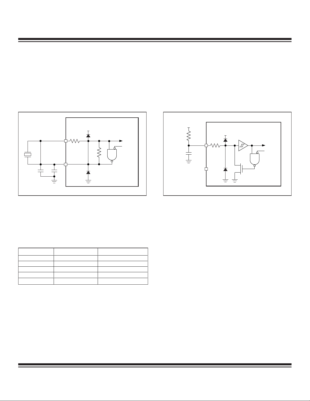
An external quartz crystal or a ceramic resonator can be connected from XTAL1 to XTAL2 as the device determining the frequency, as
illustrated in Figure 2-8. The fundamental mode of the crystal operates as inductive reactance in parallel resonance with external
capacitance to the crystal.
Crystal specifications, operating temperature, operating voltage, and parasitic capacitance must be considered when designing the
internal oscillator. To further reduce the effects of external noise, a guard ring can be placed around the oscillator circuitry.
Pins XTAL1 and XTAL2 are protected by clamping devices against on-chip electrostatic discharge. These clamping devices are diodes
parasitic to the feedback resistor Rf in the inverter circuit of the oscillator. The inverter circuit is presented as a NAND gate, which can
disable clock generation in STOP mode or if the internal ring oscillator is explicitly selected for use (i.e., RGSL = 1).
Noise at XTAL1 and XTAL2 can adversely affect on-chip clock timing. It is good design practice to place the crystal and capacitors near
the oscillator circuitry and connect to XTAL1, XTAL2, and ground with direct shot trace. The typical values of external capacitors vary
with the type of crystal used and should be initially selected based on the load capacitance as suggested by the crystal manufacturer.
For cost-sensitive applications, a ceramic resonator can be used instead of a crystal. Using the ceramic resonator may require a different circuit configuration and capacitance value.
2.7.3 External Clock (Direct Input)
The MAXQ CPU can also obtain the system clock signal directly from an external clock source. In this configuration, the clock generation circuitry is driven directly by an external clock.
To operate the core from an external clock, connect the clock source to the XTAL1 pin and leave the XTAL2 pin floating. The clock
source should be driven through a CMOS driver. If the clock driver is a TTL gate, its output must be connected to VCC through a pullup
Maxim Integrated
2-14
Page 20
PMME CD[1:0]
CYCLES PER CLOCK
0 00 1 (default)
001 2
010 4
011 8
1 xx 256
MAXQ
CLOCK
CIRCUITRY
STOP OR
RGSL
V
CC
V
CC
XTAL1
XTAL2
INTERNAL CIRCUIT
R
EXT
C
EXT
MAXQ Family User’s Guide
MAXQ
CLOCK
CIRCUITRY
STOP OR
RGSL
V
CC
XTAL1
XTAL2
C1
C2
INTERNAL CIRCUIT
R
F
resistor to ensure a satisfactory logic level for active clock pulses. To minimize system noise on the clock circuitry, the external clock
source must meet the maximum rise and fall times and the minimum high and low times specified for the clock source. The external
noise can affect clock generation circuit if these parameters do not meet the specification.
2.7.4 External RC
For timing-insensitive applications, the external RC option offers additional cost savings. The RC oscillator frequency is a function of
the supply voltage, external resistor (Rext) and capacitor (Cext) values and tolerances, and the operating temperature. In addition to
this, the oscillator frequency varies from unit to unit due to normal process parameter variation. Figure 2-9 shows how the external RC
combination is connected to the MAXQ microcontroller.
Figure 2-8. On-Chip Crystal Oscillator
Figure 2-9. RC Relaxation Oscillator
2.7.5 Internal System Clock Generation
The internal system clock is derived from the currently selected oscillator input.
By default, one system clock cycle is generated per oscillator cycle, but the number of oscillator cycles per system clock can also be
increased by setting the Power Management Mode Enable (PMME) bit and the Clock Divide Control (CD[1:0]) register bits per Table 2-2.
Table 2-2. System Clock Rate Control Settings
2-15
Maxim Integrated
Page 21

MAXQ Family User’s Guide
2.8 Interrupts
The MAXQ provides a single, programmable interrupt vector (IV) that can be used to handle internal and external interrupts. Interrupts
can be generated from system level sources (e.g., watchdog timer) or by sources associated with the peripheral modules included in
the specific MAXQ microcontroller. Only one interrupt can be handled at a time, and all interrupts naturally have the same priority. A
programmable interrupt mask register allows software-controlled prioritization and nesting of high-priority interrupts.
2.8.1 Servicing Interrupts
For the MAXQ to service an interrupt, interrupts must be enabled globally, modularly, and locally. The Interrupt Global Enable (IGE) bit
located in the Interrupt Control (IC) register acts as a global interrupt mask. This bit defaults to 0, and it must be set to 1 before any
interrupt takes place.
The local interrupt-enable bit for a particular source is in one of the peripheral registers associated with that peripheral module, or in a
system register for any system interrupt source. Between the global and local enables are intermediate per-module and system interrupt
mask bits. These mask bits reside in the Interrupt Mask system register. By implementing intermediate per-module masking capability
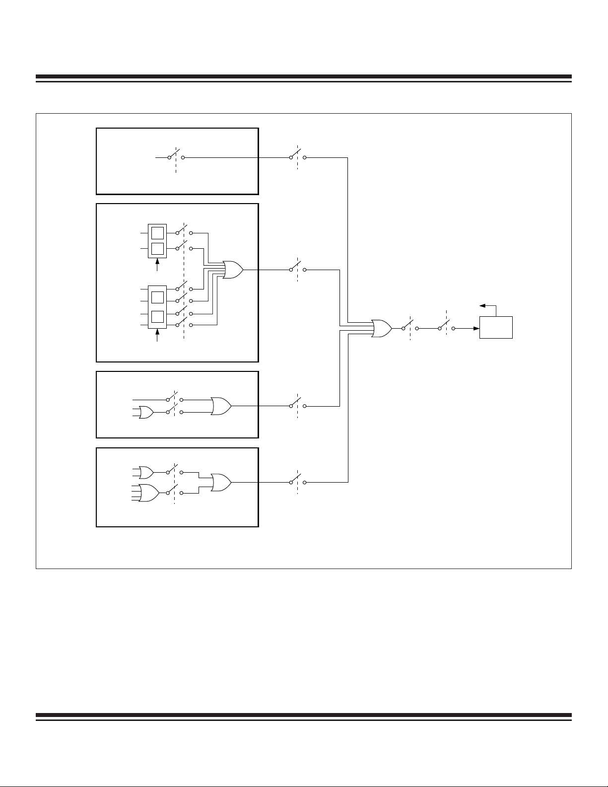
in a single register, interrupt sources spanning multiple modules can be selectively enabled/disabled in a single instruction. This promotes a simple, fast, and user-definable interrupt prioritization scheme. The interrupt source-enable hierarchy is illustrated in Figure 2-10.
When an interrupt condition occurs, its individual flag is set, even if the interrupt source is disabled at the local, module, or global level.
Interrupt flags must be cleared within the user interrupt routine to avoid repeated interrupts from the same source.
Since all interrupts vector to the address contained in the Interrupt Vector (IV) register, the Interrupt Identification Register (IIR) may be
used by the interrupt service routine to determine the module source of an interrupt. The IIR contains a bit flag for each peripheral module and one flag associated with all system interrupts; if the bit for a module is set, then an interrupt is pending that was initiated by
that module. If a module is capable of generating interrupts for different reasons, then peripheral register bits inside the module provide a means to differentiate among interrupt sources.
The Interrupt Vector (IV) register provides the location of the interrupt service routine. It may be set to any location within program memory. The IV register defaults to 0000h on reset or power-up, so if it is not changed to a different address, the user program must determine whether a jump to 0000h came from a reset or interrupt source.
2.8.2 Interrupt System Operation
The interrupt handler hardware responds to any interrupt event when it is enabled. An interrupt event occurs when an interrupt flag is
set. All interrupt requests are sampled at the rising edge of the clock and can be serviced by the processor one clock cycle later,
assuming the request does not hit the interrupt exception window. The one-cycle stall between detection and acknowledgement/servicing is due to the fact that the current instruction may also be accessing the stack. For this reason, the CPU must allow the current
instruction to complete before pushing the stack and vectoring to IV. If an interrupt exception window is generated by the currently executing instruction, the following instruction must be executed, so the interrupt service routine will be delayed an additional cycle.
Interrupt operation in the MAXQ CPU is essentially a state machine generated long CALL instruction. When the interrupt handler services an interrupt, it temporarily takes control of the CPU to perform the following sequence of actions:
1) The next instruction fetch from program memory is cancelled.
2) The return address is pushed on to the stack.
3) The INS bit is set to 1 to prevent recursive interrupt calls.
4) The instruction pointer is set to the location of the interrupt service routine (contained in the Interrupt Vector register).
5) The CPU begins executing the interrupt service routine.
Once the interrupt service routine completes, it should use the RETI instruction to return to the main program. Execution of RETI
involves the following sequence of actions:
1) The return address is popped off the stack.
2) The INS bit is cleared to 0 to re-enable interrupt handling.
3) The instruction pointer is set to the return address that was popped off the stack.
4) The CPU continues execution of the main program.
Pending interrupt requests will not interrupt an RETI instruction; a new interrupt will be serviced after first being acknowledged in the
execution cycle which follows the RETI instruction and then after the standard one stall cycle of interrupt latency. This means there will
be at least two cycles between back-to-back interrupts.
Maxim Integrated
2-16
Page 22
SYSTEM MODULES
WATCHDOG
EWDI
(LOCAL ENABLE)
TIMER/COUNTER MODULE
TF0
TF1
EXF1
SPIC
MODF
ET0, ET1
(LOCAL ENABLES)
IMx
(MODULE ENABLE)
GPI/O MODULE
INT0
EX0-EX5
(LOCAL ENABLES)
IT0
INT1
INT2
INT3
IT1
INT4
INT5
IMx
(MODULE ENABLE)
IMS
(SYSTEM ENABLE)
SERIAL I/O MODULE
RI
TI
ESI, ESPII
(LOCAL ENABLES)
IMx
(MODULE ENABLE)
ROVR
WCOL
IGE
(GLOBAL ENABLE)
NOTE: ONLY A FEW OF THE MANY POSSIBLE MAXQ PERIPHERAL MODULES ARE SHOWN IN THIS INTERRUPT
HIERARCHY FIGURE. PLEASE REFERENCE THE CORRESPONDING DATA SHEET FOR INTERRUPT FLAG
AND ENABLE BITS SPECIFIC TO A GIVEN DEVICE.
INS
(INTERRUPT IN SERVICE)
INTERRUPT
VECTOR
ƒ
ƒ
ƒ
ƒ
MAXQ Family User’s Guide
Figure 2-10. MAXQ Interrupt Source Hierarchy Example
2.8.3 Synchronous vs. Asynchronous Interrupt Sources
Interrupt sources can be classified as either asynchronous or synchronous. All internal interrupts are synchronous interrupts. An internal
interrupt is directly routed to the interrupt handler that can be recognized in one cycle. All external interrupts are asynchronous interrupts
by nature. When the device is not in Stop Mode, asynchronous interrupt sources are passed through a 3-clock sampling/glitch filter circuit before being routed to the interrupt handler. The sampling/glitch filter circuit is running on the undivided source clock (i.e., before
PMME, CD1:0-controlled clock divide) such that the number of system clocks required to recognize an asynchronous interrupt request
depends upon the system clock divide ratio:
• if the system clock divide ratio is 1, the interrupt request is recognized after 3 system clock;
2-17
Maxim Integrated
Page 23

MAXQ Family User’s Guide
• if the system clock divide ratio is 2, the interrupt request is recognized after 2 system clock;
• if the system clock divide ratio is 4 or greater, the interrupt request is recognized after 1 system clock;
An interrupt request with a pulse width less than three undivided clock cycles is not recognized. Note that the granularity of interrupt
source is at module level. Synchronous interrupts and sampled asynchronous interrupts assigned to the same module product a single interrupt to the interrupt handler.
External interrupts, when enabled, can be used as switchback sources from power management mode. There is no latency associated with the switchback because the circuit is being clocked by an undivided clock source versus the divide-by-256 system clock. For
the same reason, there is no latency for other switchback sources that do not qualify as interrupt sources.
2.8.4 Interrupt Prioritization by Software
All interrupt sources of the MAXQ microcontroller naturally have the same priority. However, when CPU operation vectors to the programmed Interrupt Vector address, the order in which potential interrupt sources are interrogated is left entirely up to the user, as this
often depends upon the system design and application requirements. The Interrupt Mask system register provides the ability to knowingly block interrupts from modules considered to be of lesser priority and manually re-enable the interrupt servicing by the CPU (by setting INS = 0). Using this procedure, a given interrupt service routine can continue executing, only to be interrupted by higher priority
interrupts. An example demonstrating this software prioritization is provided in the Handling Interrupts section of Section 3: Programming.
2.8.5 Interrupt Exception Window
An interrupt exception window is a noninterruptable execution cycle. During this cycle, the interrupt handler does not respond to any interrupt requests. All interrupts that would normally be serviced during an interrupt exception window are delayed until the next execution cycle.
Interrupt exception windows are used when two or more instructions must be executed consecutively without any delays in between.
Currently, there is a single condition in the MAXQ microcontroller that causes an interrupt exception window: activation of the prefix
(PFX) register.
When the prefix register is activated by writing a value to it, it retains that value only for the next clock cycle. For the prefix value to be
used properly by the next instruction, the instruction that sets the prefix value and the instruction that uses it must always be executed back to back. Therefore, writing to the PFX register causes an interrupt exception window on the next cycle. If an interrupt occurs
during an interrupt exception window, an additional latency of one cycle in the interrupt handling will be caused as the interrupt will
not be serviced until the next cycle.
2.9 Operating Modes
In addition to the standard program execution mode, there are three other operating modes for the MAXQ. During Reset Mode, the
processor is temporarily halted by an external or internal reset source. During Power Management Mode, the processor executes
instructions at a reduced clock rate to decrease power consumption. Stop Mode halts execution and all internal clocks to save power
until an external stimulus indicates that processing should be resumed.
2.9.1 Reset Mode
When the MAXQ microcontroller is in Reset Mode, no instruction execution or other system or peripheral operations occur, and all
input/output pins return to default states. Once the condition that caused the reset (whether internal or external) is removed, the processor begins executing code at address 8000h.
There are four different sources that can cause the MAXQ to enter Reset Mode:
• Power-On/Brownout Reset
• External Reset
• Watchdog Timer Reset
• Internal System Reset
2.9.1.1 Power-On/Brownout Reset
An on-chip power-on reset (POR) circuit is provided to ensure proper initialization on internal device states. The power-on reset circuit
provides a minimum power-on-reset delay sufficient to accomplish this initialization. For fast V
will, at a minimum, be held in reset for the power-on reset delay when initially powered up. For slow VDDsupply rise times, the MAXQ
device will be held in reset until VDDis above the power-on-reset voltage threshold. The minimum POR delay and POR voltage threshold can differ depending upon MAXQ device. Refer to the device data sheet(s) for specifics.
supply rise times, the MAXQ device
DD
Maxim Integrated
2-18
Page 24

MAXQ Family User’s Guide
Certain MAXQ devices may also incorporate brownout detection capability. For these devices, an on-chip precision reference and
comparator monitor the supply voltage VDDto ensure that it is within acceptable limits. If VDDis below the power-fail level, the power
monitor initiates a reset condition. This can occur either when the MAXQ is first powered up when the VDDsupply is above the POR
voltage threshold, or when V
In either case, the reset condition is maintained until V
following any necessary clock warmup delay.
When the processor exits from the power-on/brownout reset state, the POR bit in the Watchdog Control Register (WDCN) is set to 1
and can only be cleared by software. The user software can examine the POR bit following a reset to determine whether the reset was
caused by a power-on reset or by another source.
2.9.1.2 External Reset
During normal operation, the MAXQ device is placed into external reset mode by holding the RST pin at logic 0 for at least four clock
cycles. If MAXQ device is in the low-power Stop mode (i.e., system clock is not active), the RST pin becomes an asynchronous source,
forcing the reset state immediately after being taken to logic 0. Once the MAXQ enters Reset mode, it remains in reset as long as the
RST pin is held at logic 0. After the RST pin returns to logic 1, the processor exits the reset state within four clock cycles and begins
program execution at address 8000h.
For many MAXQ devices, the RST pin is an output as well as an input. If a reset condition is caused by another source (such as a
brownout reset, watchdog, or internal reset), an output reset pulse is generated at the RST pin for as long as the MAXQ remains in
reset. If the RST pin is connected to an RC r
if this occurs it does not affect the internal reset condition.
drops out of tolerance from an acceptable level.
DD
rises above the reset level V
DD
eset circuit or a similar circuit, it may not be able to drive the output reset signal. However
. Once VDD> V
RST
, execution may resume
RST
,
2.9.1.3 Watchdog Timer Reset
The watchdog timer is a programmable hardware timer that can be set to reset the processor in the case of a software lockup or other
unrecoverable error. Once the watchdog is enabled in this manner, the processor must reset the watchdog timer periodically to avoid
a reset. If the processor does not reset the watchdog timer before it elapses, the watchdog will initiate a reset state.
If the watchdog resets the processor, it remains in reset, and holds the RST pin low, for four clock cycles. Once the reset condition is
removed, the processor will begin executing program code at address 8000h. When a reset occurs due to a watchdog timeout, the
Watchdog Timer Reset flag in the WDCN register is set to 1 and can only be cleared by software. User software can examine this bit
following a reset to determine if that r
eset was caused by a watchdog timeout.
2.9.1.4 Internal System Reset
MAXQ devices may incorporate functions that logically warrant the ability to generate an internal system reset. This reset generation
capability is assessed by MAXQ function based upon its expected use. In-system programming is a prime example of functionality that
benefits by having the ability to reset the device. The exact in-system programming protocol is somewhat device and interface specific, however, it is expected that, upon completion of in-system programming, many users want the ability to reset the system. This
internal (software-triggered) reset generation capability is possible following in-system programming.
2.9.2 Power Management Mode
There are two major sources of power dissipation in CMOS circuitry. The first is static dissipation caused by continuous leakage current. The second is dynamic dissipation caused by transient switching current required to charge and discharge load capacitors, as
well as short circuit current produced by momentary connections between V
Usually, it is the dynamic switching power dissipation that dominates the total power consumption, and this power dissipation (P
a CMOS circuit can be calculated in terms of load capacitance (CL), power-supply voltage (VDD) and operating frequency (f) as:
P
= CLx V
D
Capacitance and supply voltage are technology dependent and relatively fixed. However, the operating frequency determines the clock
rate, and the required clock rate may be different from application to application depending on the amount of processing power required.
If an external crystal or oscillator is being used, the operating frequency can be adjusted by changing external components. However,
it may be the case that a single application may require maximum processing power at some times and very little at others. Power
Management mode allows an application to reduce its clock frequency, and therefore its power consumption, under software control.
Power Management Mode is invoked by setting the PMME bit to 1. Once this bit has been set, one system clock cycle will occur every
256 oscillator cycles. All operations continue as normal in this mode, but at the reduced clock rate. Power Management Mode can be
deactivated by clearing the PMME bit to 0; the PMME bit will also be cleared automatically to 0 by any reset condition.
DD
2
and ground during gate switching.
DD
x f
D
) for
2-19
Maxim Integrated
Page 25

MAXQ Family User’s Guide
The PMME bit may not be set to 1 if any potential switchback source is active. Attempts to set the PMME bit under these conditions
result in a no-op.
2.9.2.1 Switchback
When Power Management Mode is active, the MAXQ operates at a reduced clock rate. Although execution continues as normal,
peripherals that base their timing on the system clock such as the UART module and the SPI module may be unable to operate normally or at a high enough speed for proper application response. Additionally, interrupt latency is greatly increased.
The Switchback feature is used to allow a processor running under Power Management Mode to switch back to normal mode quickly
under certain conditions that require rapid response. Switchback is enabled by setting the SWB bit to 1. If Switchback is enabled, a
processor running under Power Management Mode automatically clears the PMME bit to 0 and returns to normal mode when any of
the following conditions occur:
• An external interrupt condition occurs on an INTx pin and the corresponding external interrupt is enabled.
• An active-low transition occurs on the UART serial receive-input line (modes 1, 2, and 3) and data reception is enabled.
• The SBUF register is written to send an outgoing byte through the UART and transmission is enabled.
• The SPIB register is written in master mode (STBY = 1) to send an outgoing character through the SPI module and transmission is enabled.
• The SPI module’s SSEL signal is asserted in slave mode.
• Time-of-Day and Subsecond interval alar
Active debug mode is enter
•
ed either by br
om the R
ms fr
eak point match or issuance of the 'Debug' command fr
TC when enabled.
om backgr
ound mode.
2.9.3 Stop Mode
When the MAXQ is in Stop Mode, the CPU system clock is stopped, and all processing activity is halted. All on-chip peripherals requiring the system clock are also stopped. Power consumption in Stop Mode is at the lowest possible level and is basically limited to static leakage current.
Stop Mode is entered by setting the STOP bit to 1. The processor enters Stop Mode immediately once the instruction that sets the STOP
bit is executed. The MAXQ exits Stop Mode when any of the following conditions occur:
• An external interrupt condition occurs on one of the INTx pins and the corresponding external interrupt is enabled. After the interrupt returns, execution resumes after the stop point.
• An external reset signal is applied to the RST pin. After the reset signal is removed, execution r
reset state.
In some MAXQ devices, the brownout voltage detection circuitry can be disabled during Stop Mode, so a power-fail condition does
not cause a reset as it would under normal conditions. Once the processor exits Stop Mode, it resumes execution as follows:
• If the RGSL bit is set to 0, the clock sour
period, the internal ring oscillator may be used for execution. The clock source switches fr
automatically once the warmup completes. The RGMD bit can be read by the processor to determine when the switch from the ring
oscillator to the XT/RC source has occurred.
• If the RGSL bit is set to 1, the inter
disabled.
ce selected by the XT/RC bit is enabled so that it may warm up/stabilize. During the warmup
nal ring oscillator will be used to resume execution and the XT/RC selected clock sour
esumes at 8000h as it would after any
om the ring oscillator to the XT/RC source
ce will remain
Maxim Integrated
2-20
Page 26

MAXQ Family User’s Guide
SECTION 3: PROGRAMMING
This section contains the following information:
3.1 Addressing Modes . . . . . . . . . . . . . . . . . . . . . . . . . . . . . . . . . . . . . . . . . . . . . . . . . . . . . . . . . .3-3
3.2 Prefixing Operations . . . . . . . . . . . . . . . . . . . . . . . . . . . . . . . . . . . . . . . . . . . . . . . . . . . . . . . . .3-3
3.3 Reading and Writing Registers . . . . . . . . . . . . . . . . . . . . . . . . . . . . . . . . . . . . . . . . . . . . . . . .3-4
3.3.1 Loading an 8-Bit Register With an Immediate Value . . . . . . . . . . . . . . . . . . . . . . . . . . .3-4
3.3.2 Loading a 16-Bit Register With a 16-Bit Immediate Value . . . . . . . . . . . . . . . . . . . . . . .3-4
3.3.3 Moving Values Between Registers of the Same Size . . . . . . . . . . . . . . . . . . . . . . . . . . .3-4
3.3.4 Moving Values Between Registers of Different Sizes . . . . . . . . . . . . . . . . . . . . . . . . . . .3-4
3.4 Reading and Writing Register Bits . . . . . . . . . . . . . . . . . . . . . . . . . . . . . . . . . . . . . . . . . . . . . .3-6
3.5 Using the Arithmetic and Logic Unit . . . . . . . . . . . . . . . . . . . . . . . . . . . . . . . . . . . . . . . . . . . .3-6
3.5.1 Selecting the Active Accumulator . . . . . . . . . . . . . . . . . . . . . . . . . . . . . . . . . . . . . . . . . .3-6
3.5.2 Enabling Auto-Increment and Auto-Decrement . . . . . . . . . . . . . . . . . . . . . . . . . . . . . . .3-6
3.5.3 ALU Operations Using the Active Accumulator and a Source . . . . . . . . . . . . . . . . . . .3-8
3.5.4 ALU Operations Using Only the Active Accumulator . . . . . . . . . . . . . . . . . . . . . . . . . . .3-9
3.5.5 ALU Bit Operations Using Only the Active Accumulator . . . . . . . . . . . . . . . . . . . . . . . .3-9
3.5.6 MAXQ10 Example: Adding Two 4-Byte Numbers Using Auto-Increment . . . . . . . . . . .3-9
3.5.7 MAXQ20 Example: Adding Two 4-Byte Numbers Using Auto-Increment . . . . . . . . . . .3-10
3.6 Processor Status Flag Operations . . . . . . . . . . . . . . . . . . . . . . . . . . . . . . . . . . . . . . . . . . . . . .3-10
3.6.1 Sign Flag . . . . . . . . . . . . . . . . . . . . . . . . . . . . . . . . . . . . . . . . . . . . . . . . . . . . . . . . . . . . .3-10
3.6.2 Zero Flag . . . . . . . . . . . . . . . . . . . . . . . . . . . . . . . . . . . . . . . . . . . . . . . . . . . . . . . . . . . . .3-10
3.6.3 Equals Flag . . . . . . . . . . . . . . . . . . . . . . . . . . . . . . . . . . . . . . . . . . . . . . . . . . . . . . . . . . .3-10
3.6.4 Carry Flag . . . . . . . . . . . . . . . . . . . . . . . . . . . . . . . . . . . . . . . . . . . . . . . . . . . . . . . . . . . .3-10
3.6.5 Overflow Flag . . . . . . . . . . . . . . . . . . . . . . . . . . . . . . . . . . . . . . . . . . . . . . . . . . . . . . . . .3-11
3.7 Controlling Program Flow . . . . . . . . . . . . . . . . . . . . . . . . . . . . . . . . . . . . . . . . . . . . . . . . . . . . .3-11
3.7.1 Obtaining the Next Execution Address . . . . . . . . . . . . . . . . . . . . . . . . . . . . . . . . . . . . .3-11
3.7.2 Unconditional Jumps . . . . . . . . . . . . . . . . . . . . . . . . . . . . . . . . . . . . . . . . . . . . . . . . . . .3-12
3.7.3 Conditional Jumps . . . . . . . . . . . . . . . . . . . . . . . . . . . . . . . . . . . . . . . . . . . . . . . . . . . . .3-12
3.7.4 Calling Subroutines . . . . . . . . . . . . . . . . . . . . . . . . . . . . . . . . . . . . . . . . . . . . . . . . . . . . .3-12
3.7.5 Looping Operations . . . . . . . . . . . . . . . . . . . . . . . . . . . . . . . . . . . . . . . . . . . . . . . . . . . .3-12
3.7.6 Conditional Returns . . . . . . . . . . . . . . . . . . . . . . . . . . . . . . . . . . . . . . . . . . . . . . . . . . . .3-13
3-1
Maxim Integrated
Page 27

MAXQ Family User’s Guide
3.8 Handling Interrupts . . . . . . . . . . . . . . . . . . . . . . . . . . . . . . . . . . . . . . . . . . . . . . . . . . . . . . . . . .3-13
3.8.1 Conditional Return from Interrupt . . . . . . . . . . . . . . . . . . . . . . . . . . . . . . . . . . . . . . . . . .3-14
3.9 Accessing the Stack . . . . . . . . . . . . . . . . . . . . . . . . . . . . . . . . . . . . . . . . . . . . . . . . . . . . . . . . .3-15
3.10 Accessing Data Memory . . . . . . . . . . . . . . . . . . . . . . . . . . . . . . . . . . . . . . . . . . . . . . . . . . . .3-15
3.11 Using the Watchdog Timer . . . . . . . . . . . . . . . . . . . . . . . . . . . . . . . . . . . . . . . . . . . . . . . . . . .3-17
LIST OF FIGURES
Figure 3-1. Watchdog Timer Block Diagram . . . . . . . . . . . . . . . . . . . . . . . . . . . . . . . . . . . . . . . . .3-18
LIST OF TABLES
Table 3-1. Accumulator Pointer Control Register Settings . . . . . . . . . . . . . . . . . . . . . . . . . . . . . . .3-7
Table 3-2. Watchdog Timer Register Control Bits . . . . . . . . . . . . . . . . . . . . . . . . . . . . . . . . . . . . .3-17
Table 3-3. Watchdog Timeout Period Selection . . . . . . . . . . . . . . . . . . . . . . . . . . . . . . . . . . . . . . .3-19
Table 3-4. System Register Map . . . . . . . . . . . . . . . . . . . . . . . . . . . . . . . . . . . . . . . . . . . . . . . . . .3-19
Table 3-5. System Register Bit Map . . . . . . . . . . . . . . . . . . . . . . . . . . . . . . . . . . . . . . . . . . . . . . . .3-20
Table 3-6. System Register Bit Reset Values . . . . . . . . . . . . . . . . . . . . . . . . . . . . . . . . . . . . . . . . .3-21
Maxim Integrated
3-2
Page 28

MAXQ Family User’s Guide
SECTION 3: PROGRAMMING
The following section provides a programming overview of the MAXQ. For full details on the instruction set, as well as System Register
and Peripheral Register detailed bit descriptions, see the appropriate sections in this user’s guide.
3.1 Addressing Modes
The instruction set for the MAXQ provides three different addressing modes: direct, indirect, and immediate.
The direct addressing mode can be used to specify either source or destination registers, such as:
move A[0], A[1] ; copy accumulator 1 to accumulator 0
push A[0]
add A[1] ; add accumulator 1 to the active accumulator
Direct addressing is also used to specify addressable bits within registers.
move C, Acc.0 ; copy bit zero of the active accumulator
move PO0.3, #1 ; set bit three of port 0 Output register
Indirect addressing, in which a register contains a source or destination address, is used only in a few cases.
move @DP[0], A[0] ; copy accumulator 0 to the data memory
move A[0], @SP-- ; where @SP-- is used to pop the data pointed to
; push accumulator 0 on the stack
; to the carry flag
; location pointed to by data pointer 0
; by the stack pointer register
Immediate addr
essing is used to provide values to be directly loaded into registers or used as operands.
move A[0], #10h ; set accumulator 1 to 10h/16d
3.2 Prefixing Operations
All instructions on the MAXQ are 16 bits long and execute in a single cycle. However, some operations require more data than can be
specified in a single cycle or require that high-order register-index bits be set to achieve the desired transfer. In these cases, the prefix register module PFX is loaded with temporary data and/or required register index bits to be used by the following instruction. The
PFX module only holds loaded data for a single cycle before it clears to zero.
Instruction prefixing is required for the following operations, which effectively makes them two-cycle operations:
• When providing a 16-bit immediate value for an operation (e.g., loading a 16-bit register, ALU operation, supplying an absolute pro-
gram branch destination), the PFX module must be loaded in the previous cycle with the high byte of the 16-bit immediate value
unless that high byte is zero. One exception to this rule is when supplying an absolute branch destination to 00xxh. In this case,
PFX still must be written with 00h. Otherwise, the branch instruction would be considered a relative one instead of the desired
absolute branch.
• When selecting registers with indexes greater than 07h within a module as destinations for a transfer or registers with indexes
greater than 0Fh within a module as sources, the PFX[n] register must be loaded in the previous cycle. This can be combined with
the previous item.
Generally, prefixing operations can be inserted automatically by the assembler as needed, so that (for example)
move DP[0], #1234h
actually assembles as
move PFX[0], #12h
move DP[0], #34h
However, the operation
move DP[0], #0055h
does not require a prefixing operation even though the register DP[0] is 16-bit. This is because the prefix value defaults to zero, so the line
move PFX[0], #00h
is not required.
3-3
Maxim Integrated
Page 29

MAXQ Family User’s Guide
3.3 Reading and Writing Registers
All functions in the MAXQ are accessed through registers, either directly or indirectly. This section discusses loading registers with
immediate values and transferring values between registers of the same size and different sizes.
3.3.1 Loading an 8-Bit Register With an Immediate Value
Any writeable 8-bit register with a sub-index from 0h to 7h within its module can be loaded with an immediate value in a single cycle
using the MOVE instruction.
move AP, #05h ; load accumulator pointer register with 5 hex
Writeable 8-bit registers with sub-indexes 8h and higher can be loaded with an immediate value using MOVE as well, but an additional
cycle is required to set the prefix value for the destination.
move WDCN, #33h ; assembles to: move PFX[2], #00h
; move (WDCN-80h), #33h
3.3.2 Loading a 16-Bit Register With a 16-Bit Immediate Value
Any writeable 16-bit register with a sub-index from 0h to 07h can be loaded with an immediate value in a single cycle if the high byte
of that immediate value is zero.
move LC[0], #0010h ; prefix defaults to zero for high byte
If the high byte of that immediate value is not zero or if the 16-bit destination sub-index is greater than 7h, an extra cycle is required to
load the prefix value for the high byte and/or the high-order register index bits.
; high byte <> #00h
move LC[0], #0110h ; assembles to: move PFX[0], #01h
; move LC[0], #10h
; destination sub-index > 7h
move A[8], #0034h ; assembles to: move PFX[2], #00h
; move (A[8]-80h), #34h
3.3.3 Moving Values Between Registers of the Same Size
Moving data between same-size registers can be done in a single-cycle MOVE if the destination register’s index is from 0h to 7h and
the source register index is between 0h and Fh.
move A[0], A[8] ; copy accumulator 8 to accumulator 0
move LC[0], LC[1] ; copy loop counter 1 to loop counter 0
If the destination register’s index is greater than 7h or if the source register index is greater than Fh, prefixing is required.
move A[15], A[0] ; assembles to: move PFX[2], #00h
; move (A[15]-80h), A[0]
3.3.4 Moving Values Between Registers of Different Sizes
Before covering some transfer scenarios that might arise, a special register must be introduced that will be used in many of these
cases. The 16-bit General Register (GR) is expressly provided for performing byte singulation of 16-bit words. The high and low bytes
of GR are individually accessible in the GRH and GRL registers respectively. A read-only GRS register makes a byte-swapped version
of GR accessible and the GRXL register provides a sign-extended version of GRL.
8-bit destination ← low byte (16-bit source)
The simplest transfer possibility would be loading an 8-bit register with the low byte of a 16-bit register. This transfer does not require
use of GR and requires a prefix only if the destination or source register are outside of the single cycle write or read regions, 0–7h and
0–Fh, respectively.
move OFFS, LC[0] ; copy the low byte of LC[0] to the OFFS register
move IMR, @DP[1] ; copy the low byte @DP[1] to the IMR register
move WDCN, LC[0] ; assembles to: move PFX[2], #00h
; move (WDCON-80h), LC[0]
Maxim Integrated
3-4
Page 30

MAXQ Family User’s Guide
8-bit destination ← high byte (16-bit source)
If, however, we needed to load an 8-bit register with the high byte of a 16-bit source, it would be best to use the GR register. Transferring
the 16-bit source to the GR register adds a single cycle.
move GR, LC[0] ; move LC[0] to the GR register
move IC, GRH ; copy the high byte into the IC register
16-bit destination ← concatenation (8-bit source, 8-bit source)
Two 8-bit source registers can be concatenated and stored into a 16-bit destination by using the prefix register to hold the high-order
byte for the concatenated transfer. An additional cycle may be required if either source byte register index is gr
16-bit destination is greater than 07h.
move PFX[0], IC ; load high order source byte IC into PFX
move @++SP, AP ; store @DP[0] the concatenation of IC:AP
; 16-bit destination sub-index: dst=08h
; 8-bit source sub-indexes:
; high=10h, low=11h
move PFX[1], #00h ;
move PFX[3], high ; PFX=00:high
move dst, low ; dst=high:low
Low (16-bit destination) ← 8-bit source
To modify only the low byte of a given 16-bit destination, the 16-bit register should be moved into the GR register such that the high
byte can be singulated and the low byte written exclusively. An additional cycle is required if the destination index is greater than 0Fh.
move GR, DP[0] ;
move PFX[0], GRH ; get the high byte of DP[0] via GRH
move DP[0], #20h ; store the new DP[0] value
move PFX[1], #00h ;
move GR, dst ; read dst word to the GR register
move PFX[5], GRH ; get the high byte of dst via GRH
move dst, src ; store the new dst value
High (16-bit destination) ← 8-bit source
To modify only the high byte of a given 16-bit destination, the 16-bit register should be moved into the GR r
byte can be singulated and the high byte can be written exclusively. Additional cycles are requir
than 0Fh or if the source index is greater than 0Fh.
move GR, DP[0] ; move DP[0] to the GR register
move PFX[0], #20h ; get the high byte of DP[0] via GRH
move DP[0], GRL ; store the new DP[0] value
move PFX[1], #00h ;
move GR, dst ; read dst word to the GR register
move PFX[1], #00h
move PFX[4], src ; get the new src byte
move dst, GRL ; store the new dst value
If the high byte needs to be clear
(example follows):
move GR, DP[0] ; move DP[0] to the GR register
move DP[0], GRL ; store the new DP[0] value, 00h used for high byte
ed to 00h, the operation can be shortened by transferring only the GRL byte to the 16-bit destination
move DP[0] to the GR register
; 16-bit destination sub-index: dst=10h
; 8-bit source sub-index: src=11h
ed if the destination index is greater
; 16-bit destination sub-index: dst=10h
; 8-bit source sub-index: src=11h
eater than 0Fh or the
egister such that the low
3-5
Maxim Integrated
Page 31

MAXQ Family User’s Guide
3.4 Reading and Writing Register Bits
The MOVE instruction can also be used to directly set or clear any one of the lowest 8 bits of a peripheral register in module 0h-5h or
a system register in module 8h. The set or clear operation will not affect the upper byte of a 16-bit register that is the target of the set
or clear operation. If a set or clear instruction is used on a destination register that does not support this type of operation, the register high byte will be written with the prefix data and the low byte will be written with the bit mask (i.e. all 0’s with a single 1 for the set
bit operation or all ones with a single 0 for the clear bit operation).
Register bits can be set or cleared individually using the MOVE instruction as follows.
move IGE, #1 ; set IGE (Interrupt Global Enable) bit
move APC.6, #0
As with other instructions, prefixing is required to select destination registers beyond index 07h.
The MOVE instruction may also be used to transfer any one of the lowest 8 bits from a register source or any bit of the active accumulator (Acc) to the Carry flag. There is no restriction on the sour
move C, IIR.3 ; copy IIR.3 to Carry
move C, Acc.7
Prefixing is requir
ed to select source registers beyond index 15h.
3.5 Using the Arithmetic and Logic Unit
The MAXQ provides either an 8-bit (MAXQ10) or 16-bit (MAXQ20) ALU, which allows operations to be performed between the active
accumulator and any other register. The default ALU configuration provides eight accumulator registers that are also either 8-bit
(MAXQ10) or 16-bit (MAXQ20) wide, of which any one may be selected as the active accumulator. Many MAXQ devices will be
equipped with 16 working accumulators.
; clear IDS bit (APC.6)
ce register module for the ‘MOVE C, src.bit’ instruction.
; copy Acc.7 to Carry
3.5.1 Selecting the Active Accumulator
Any of the 16 accumulator registers A[0] through A[15] may be selected as the active accumulator by setting the low four bits of the
Accumulator Pointer Register (AP) to the index of the accumulator register you want to select.
move AP, #01h ; select A[1] as the active accumulator
move AP, #0Fh ; select A[15] as the active accumulator
The current active accumulator can be accessed as the Acc register, which is also the register used as the implicit destination for all
arithmetic and logical operations.
move A[0], #55h ; set A[0] = 55 hex (MAXQ10)
; = 0055 hex (MAXQ20)
move AP, #00h ; select A[0] as active accumulator
move Acc, #55h ; set A[0] = 55 hex (MAXQ10)
; = 0055 hex (MAXQ20)
3.5.2 Enabling Auto-Increment and Auto-Decrement
The accumulator pointer AP can be set to automatically increment or decrement after each arithmetic or logical operation. This is useful for operations involving a number of accumulator registers, such as adding or subtracting two multibyte integers.
If auto-increment/decrement is enabled, the AP register increments or decrements after any of the following operations:
• ADD src (Add source to active accumulator)
• ADDC src (Add source to active accumulator with carry)
• SUB src (Subtract source from active accumulator)
• SUBB src (Subtract source from active accumulator with borrow)
• AND src (Logical AND active accumulator with source)
• OR src (Logical OR active accumulator with source)
• XOR src (Logical XOR active accumulator with source)
• CPL (Bit-wise complement active accumulator)
• NEG (Negate active accumulator)
Maxim Integrated
3-6
Page 32

APC.2
(MOD2)
APC.1
(MOD1)
APC.0
(MOD0)
APC.6
(IDS)
APC AUTO INCREMENT/DECREMENT SETTING
000X00h
No auto-increment/decrement (default mode)
001001h
Increment bit 0 of AP (modulo 2)
001141h
Decrement bit 0 of AP (modulo 2)
010002h
Increment bits [1:0] of AP (modulo 4)
010142h
Decrement bits [1:0] of AP (modulo 4)
011003h
Increment bits [2:0] of AP (modulo 8)
011143h
Decrement bits [2:0] of AP (modulo 8)
100004h
Increment all 4 bits of AP (modulo 16)
100144h
Decrement all 4 bits of AP (modulo 16)
MAXQ Family User’s Guide
• SLA (Arithmetic shift left on active accumulator)
• SLA2 (Arithmetic shift left active accumulator two bit positions)
• SLA4 (Arithmetic shift left active accumulator four bit positions)
• SRA (Arithmetic shift right on active accumulator)
• SRA2 (Arithmetic shift right active accumulator two bit positions)
• SRA4 (Arithmetic shift right active accumulator four bit positions)
• RL (Rotate active accumulator left)
• RLC (Rotate active accumulator left through Carry flag)
• RR (Rotate active accumulator right)
• RRC (Rotate active accumulator right through Carry flag)
• SR (Logical shift active accumulator right)
• MOVE Acc, src (Copy data from source to active accumulator)
• MOVE dst, Acc (Copy data from active accumulator to destination)
• MOVE Acc, Acc (Recirculation of active accumulator contents)
• XCHN (Exchange nibbles within each byte of active accumulator)
(MAXQ20 Only)
• XCH (Exchange active accumulator bytes)
The active accumulator may not be the sour
There is an additional notation that can be used to refer to the active accumulator for the instruction "MOVE dst, Acc." If the instruction
is instead written as "MOVE dst, A[AP]," the source value is still the active accumulator, but no AP auto-increment or auto-decrement
function will take place, even if this function is enabled. Note that the active accumulator may not be the destination for the MOVE dst,
A[AP] instruction (i.e. MOVE Acc, A[AP] is prohibited).
So, the two instructions
move A[7], Acc
move A[7], A[AP]
are equivalent, except that the first instruction triggers auto-inc/dec (if it is enabled), while the second one will never do so.
The Accumulator Pointer Contr
ol Register (APC) controls the automatic-incr
(modulo) in the AP register that will be incremented or decremented. There are nine different unique settings for the APC r
listed in Table 3-1.
ce in any instruction where it is also the implicit destination.
ement/decrement mode as well as selects the range of bits
egister, as
Table 3-1. Accumulator Pointer Control Register Settings
3-7
Maxim Integrated
Page 33

MAXQ Family User’s Guide
For the modulo increment or decrement operation, the selected range of bits in AP are incremented or decremented. However, if these
bits roll over or under, they simply wrap around without affecting the remaining bits in the accumulator pointer. So, the operations can
be defined as follows:
• Increment modulo 2: AP = AP[3:1] + ((AP[0] + 1) mod 2)
• Decrement modulo 2: AP = AP[3:1] + ((AP[0] - 1) mod 2)
• Increment modulo 4: AP = AP[3:2] + ((AP[1:0] + 1) mod 4)
• Decrement modulo 4: AP = AP[3:2] + ((AP[1:0] - 1) mod 4)
• Increment modulo 8: AP = AP[3] + ((AP[2:0] + 1) mod 8)
• Decrement modulo 8: AP = AP[3] + ((AP[2:0] - 1) mod 8)
• Increment modulo 16: AP = (AP + 1) mod 16
• Decrement modulo 16: AP = (AP - 1) mod 16
For this example, assume that all 16 accumulator registers are initially set to zero.
move AP, #02h ; select A[2] as active accumulator
move APC, #02h
add #01h ; 03 0000 0000 0001 0000
add #02h ; 00 0000 0000 0001 0002
add #03h ; 01 0003 0000 0001 0002
add #04h ; 02 0003 0004 0001 0002
add #05h ; 03 0003 0004 0006 0002
3.5.3 ALU Operations Using the Active Accumulator and a Source
The following arithmetic and logical operations can use any register or immediate value as a source. The active accumulator Acc is
always used as the second operand and the implicit destination. Also, Acc may not be used as the source for any of these operations.
add A[4] ; Acc = Acc + A[4]
addc #32h ; Acc = Acc + 32h + Carry (MAXQ10)
sub A[15] ; Acc = Acc – A[15]
subb A[1] ; Acc = Acc – A[1] - Carry
cmp #00h ; If (Acc == 00h), set Equals flag (MAXQ10)
and A[0] ; Acc = Acc AND A[0]
or #55h ; Acc = Acc OR #55h (MAXQ10)
xor A[1] ; Acc = Acc XOR A[1]
; auto-increment AP[1:0] modulo 4
; AP A[0]* A[1]* A[2]* A[3]*
; 02 0000 0000 0000 0000
;
; *the upper #00h byte of each accumulator
; is only present on the MAXQ20 device
; Acc = Acc + 0032h + Carry (MAXQ20)
; If (Acc == 0000h), set Equals flag (MAXQ20)
; Acc = Acc OR #0055h (MAXQ20)
Maxim Integrated
3-8
Page 34

MAXQ Family User’s Guide
3.5.4 ALU Operations Using Only the Active Accumulator
The following arithmetic and logical operations operate only on the active accumulator.
cpl ; Acc = NOT Acc
neg ; Acc = (NOT Acc) + 1
rl ; Rotate accumulator left (not using Carry)
rlc ; Rotate accumulator left through Carry
rr ; Rotate accumulator right (not using Carry)
rrc ; Rotate accumulator right through Carry
sla ; Shift accumulator left arithmetically once
sla2 ; Shift accumulator left arithmetically twice
sla4 ; Shift accumulator left arithmetically four times
sr ; Shift accumulator right, set Carry to Acc.0,
; set Acc.7 to zero (MAXQ10)
; set Acc.15 to zero (MAXQ20)
sra ; Shift accumulator right arithmetically once
sra2 ; Shift accumulator right arithmetically twice
sra4 ; Shift accumulator right arithmetically four times
xchn ; Swap low and high nibbles of each Acc byte
xch (MAXQ20 only) ; Swap low byte and high byte of Acc
3.5.5 ALU Bit Operations Using Only the Active Accumulator
The following operations operate on single bits of the current active accumulator in conjunction with the Carry flag. Any of these operations may use an Acc bit from 0 to 7 (for MAXQ10) or from 0 to 15 (for MAXQ20).
move C, Acc.0 ; copy bit 0 of accumulator to Carry
move Acc.5, C ; copy Carry to bit 5 of accumulator
and Acc.3 ; Acc.3 = Acc.3 AND Carry
or Acc.0 ; Acc.0 = Acc.0 OR Carry
xor Acc.1 ; Acc.1 = Acc.1 OR Carry
None of the above bit operations cause the auto-increment, auto-decrement, or modulo operations defined by the accumulator pointer control (APC) register.
3.5.6 MAXQ10 Example: Adding Two 4-Byte Numbers Using Auto-Increment
move A[0], #78h ; First number – 12345678h
move A[1], #56h
move A[2], #34h
move A[3], #12h
move A[4], #0AAh ; Second number – 0AAAAAAAh
move A[5], #0AAh
move A[6], #0AAh
move A[7], #0Ah
move AP, #00h ; A[0] is active accumulator
move APC, #02h ; Increment low two bits mod 4
add A[4] ; A[0] = 78h + AAh = 22h + Carry
addc A[5] ; A[1] = 56h + AAh + 1 = 01h + Carry
addc A[6] ; A[2] = 34h + AAh + 1 = DFh
addc A[7] ; A[3] = 12h + 0Ah = 1Ch
; 12345678h + 0AAAAAAAh = 1CDF0122h
3-9
Maxim Integrated
Page 35

MAXQ Family User’s Guide
3.5.7 MAXQ20 Example: Adding Two 4-Byte Numbers Using Auto-Increment
move A[0], #5678h ; First number – 12345678h
move A[1], #1234h
move A[2], #0AAAAh ; Second number – 0AAAAAAAh
move A[3], #0AAAh
move APC, #81h ; Active Acc = A[0], increment low bit = mod 2
add A[2] ; A[0] = 5678h + AAAAh = 0122h + Carry
addc A[3] ; A[1] = 1234h + AAAh + 1 = 1CDFh
; 12345678h + 0AAAAAAAh = 1CDF0122h
3.6 Processor Status Flag Operations
The Processor Status Flag (PSF) register contains five flags that are used to indicate and store the results of arithmetic and logical operations, four of which can also be used for conditional program branching.
3.6.1 Sign Flag
The Sign flag (PSF.6) reflects the current state of the high bit of the active accumulator (Acc.7 for the MAXQ10 or Acc.15 for the
MAXQ20). If signed arithmetic is being used, this flag indicates whether the value in the accumulator is positive or negative.
Since the Sign flag is a dynamic reflection of the high bit of the active accumulator, any instruction that changes the value in the active
accumulator can potentially change the value of the Sign flag. Also, any instruction that changes which accumulator is the active one
(including AP auto-increment/decrement) can also change the Sign flag.
The following operation uses the Sign flag:
• JUMP S, src (Jump if Sign flag is set)
3.6.2 Zero Flag
The Zero flag (PSF.7) is a dynamic flag that reflects the current state of the active accumulator Acc. If all bits in the active accumulator are zero, the Zero flag equals 1. Otherwise, it equals 0.
Since the Zero flag is a dynamic reflection of (Acc = 0), any instruction that changes the value in the active accumulator can potentially change the value of the Zero flag. Also, any instruction that changes which accumulator is the active one (including AP auto-increment/decrement) can also change the Zero flag.
The following operations use the Zero flag:
• JUMP Z, src (Jump if Zero flag is set)
• JUMP NZ, src (Jump if Zero flag is cleared)
3.6.3 Equals Flag
The Equals flag (PSF.0) is a static flag set by the CMP instruction. When the source given to the CMP instruction is equal to the active
accumulator, the Equals flag is set to 1. When the source is different from the active accumulator, the Equals flag is cleared to 0.
The following instructions use the value of the Equals flag. Please note that the ‘src’ for the JUMP E/NE instructions must be immediate.
• JUMP E, src (Jump if Equals flag is set)
• JUMP NE, src (Jump if Equals flag is cleared)
In addition to the CMP instruction, any instruction using PSF as the destination can alter the Equals flag.
3.6.4 Carry Flag
The Carry flag (PSF.1) is a static flag indicating that a carry or borrow bit resulted from the last ADD/ADDC or SUB/SUBB operation.
Unlike the other status flags, it can be set or cleared explicitly and is also used as a generic bit operand by many other instructions.
The following instructions can alter the Carry flag:
• ADD src (Add source to active accumulator)
• ADDC src (Add source and Carry to active accumulator)
• SUB src (Subtract source from active accumulator)
• SUBB src (Subtract source and Carry from active accumulator)
Maxim Integrated
3-10
Page 36

MAXQ Family User’s Guide
• SLA, SLA2, SLA4 (Arithmetic shift left active accumulator)
• SRA, SRA2, SRA4 (Arithmetic shift right active accumulator)
• SR (Shift active accumulator right)
• RLC/RRC (Rotate active accumulator left / right through Carry)
• MOVE C, Acc.<b> (Set Carry to selected active accumulator bit)
• MOVE C, #i (Explicitly set, i = 1, or clear, i = 0, the Carry flag)
• CPL C (Complement Carry)
• AND Acc.<b>
• OR Acc.<b>
• XOR Acc.<b>
• MOVE C, src.<b> (Copy bit addressable register bit to Carry)
• any instruction using PSF as the destination
The following instructions use the value of the Carry flag:
• ADDC src (Add source and Carry to active accumulator)
• SUBB src (Subtract source and Carry from active accumulator)
• RLC/RRC (Rotate active accumulator left/right through Carry)
• CPL C (Complement Carry)
• MOVE Acc.<b>, C (Set selected active accumulator bit to Carry)
• AND Acc.<b> (Carry = Carry AND selected active accumulator bit)
• OR Acc.<b> (Carry = Carry OR selected active accumulator bit)
• XOR Acc.<b> (Carry = Carry XOR selected active accumulator bit)
• JUMP C, src (Jump if Carry flag is set)
• JUMP NC, src (Jump if Carry flag is cleared)
3.6.5 Overflow Flag
The Overflow flag (PSF.2) is a static flag indicating that the carry or borrow bit (Carry status Flag) resulting from the last ADD/ADDC or
SUB/SUBB operation but did not match the carry or borrow of the high order bit of the active accumulator. The overflow flag is useful
when performing signed arithmetic operations.
The following instructions can alter the Overflow flag:
• ADD src (Add source to active accumulator)
• ADDC src (Add source and Carry to active accumulator)
• SUB src (Subtract source from active accumulator)
• SUBB src (Subtract source and Carry from active accumulator)
3.7 Controlling Program Flow
The MAXQ provides several options to control program flow and branching. Jumps may be unconditional, conditional, relative, or
absolute. Subroutine calls store the return address on the hardware stack for later return. Built-in counters and address registers are
provided to control looping operations.
3.7.1 Obtaining the Next Execution Address
The address of the next instruction to be executed can be read at any time by reading the Instruction Pointer (IP) register. This can be
particularly useful for initializing loops. Note that the value returned is actually the address of the current instruction plus 1, so this will
be the address of the next instruction executed as long as the current instruction does not cause a jump.
3-11
Maxim Integrated
Page 37

MAXQ Family User’s Guide
3.7.2 Unconditional Jumps
An unconditional jump can be relative (IP +127/-128 words) or absolute (to anywhere in program space). Relative jumps must use an
8-bit immediate operand, such as
Label1: ; must be within +127/-128 words of the JUMP
...
jump Label1
Absolute jumps can use a 16-bit immediate operand, a 16-bit register, or an 8-bit register.
jump LongJump ; assembles to: move PFX[0], #high(LongJump)
; jump #low(LongJump)
jump DP[0]
If an 8-bit register is used as the jump destination, the prefix value is used as the high byte of the address and the register is used as
the low byte.
3.7.3 Conditional Jumps
Conditional jumps transfer program execution based on the value of one of the status flags (C, E, Z, S). Except where noted for JUMP
E and JUMP NE, the absolute and relative operands allowed are the same as for the unconditional JUMP command.
jump c, Label1 ; jump to Label1 if Carry is set
jump nc, LongJump ; jump to LongJump if Carry is not set
jump z, LC[0] ; jump to 16-bit register destination if
jump nz, Label1 ; jump to Label1 if Zero is not set (Acc<>0)
jump s, A[2] ; jump to A[2] if Sign flag is set
jump e, Label1 ; jump to Label1 if Equal is set
jump ne, Label1 ; jump to Label1 if Equal is cleared
JUMP E and JUMP NE may only use immediate destinations.
; absolute jump to the address in DP[0]
; Zero is set
3.7.4 Calling Subroutines
The CALL instruction works the same as the unconditional JUMP, except that the next execution address is pushed on the stack before
transferring program execution to the branch address. The RET instruction is used to return from a normal call, and RETI is used to
return from an interrupt handler routine.
call Label1 ; if Label1 is relative,
; assembles to : call #immediate
call LongCall ; assembles to: move PFX[0], #high(LongCall)
; call #low(LongCall)
call LC[0] ; call to address in LC[0]
LongCall:
ret ; return from subroutine
3.7.5 Looping Operations
Looping over a section of code can be performed by using the conditional jump instructions. However, there is built-in functionality, in
the form of the ‘DJNZ LC[n], src’ instruction, to support faster, more compact looping code with separate loop counters. The 16-bit registers LC[0], and LC[1] are used to store these loop counts. The ‘DJNZ LC[n], src’ instruction automatically decrements the associated loop counter register and jumps to the loop address specified by src if the loop counter has not reached 0.
To initialize a loop, set the LC[n] register to the count you wish to use before entering the loop’s main body.
The desired loop address should be supplied in the src operand of the ‘DJNZ LC[n], src’ instruction. When the supplied loop address
is relative (+127/-128 words) to the DJNZ LC[n] instruction, as is typically the case, the assembler automatically calculates the relative
offset and inserts this immediate value in the object code.
move LC[1], #10h ; loop 16 times
LoopTop:
call LoopSub
djnz LC[1], LoopTop ; decrement LC[1] and jump if nonzero
; loop addr relative to djnz LC[n],src instruction
Maxim Integrated
3-12
Page 38

MAXQ Family User’s Guide
When the supplied loop address is outside the relative jump range, the prefix register (PFX[0]) is used to supply the high byte of the
loop address as required.
move LC[1], #10h ; loop 16 times
LoopTop: ; loop addr not relative to djnz LC[n],src
call LoopSub
...
djnz LC[1], LoopTop ; decrement LC[1] and jump if nonzero
; assembles to: move PFX[0], #high(LoopTop)
; djnz LC[1], #low(LoopTop)
If loop execution speed is critical and a relative jump cannot be used, one might consider preloading an internal 16-bit register with
the src loop address for the ‘DJNZ LC[n], src’ loop. This ensures that the pr
and always yields the fastest execution of the DJNZ instruction.
move LC[0], #LoopTop ; using LC[0] as address holding register
; assembles to: move PFX[0], #high(LoopTop)
; move LC[0], #low(LoopTop)
move LC[1], #10h ; loop 16 times
...
LoopTop: ; loop address not relative to djnz LC[n],src
call LoopSub
...
djnz LC[1], LC[0] ; decrement LC[1] and jump if nonzero
If opting to preload the loop address to an inter
the instruction just prior to the top of the loop:
move LC[1], #10h ; Set loop counter to 16
move LC[0], IP ; Set loop address to the next address
LoopTop: ; loop addr not relative to djnz LC[n],src
...
nal 16-bit register, the most time and code efficient means is by performing the load in
3.7.6 Conditional Returns
Similar to the conditional jumps, the MAXQ microcontroller also supports a set of conditional return operations. Based upon the value
of one of the status flags, the CPU can conditionally pop the stack and begin execution at the address popped from the stack. If the
condition is not true, the conditional return instruction does not pop the stack and does not change the instruction pointer. The following conditional return operations are supported:
RET C ; if C=1, a RET is executed
RET NC ; if C=0, a RET is executed
RET Z ; if Z=1 (Acc=00h), a RET is executed
RET NZ ; if Z=0 (Acc<>00h), a RET is executed
RET S ; if S=1, a RET is executed
efix register will not be needed to supply the loop address
3.8 Handling Interrupts
Handling interrupts in the MAXQ is a three-part process. First, the location of the interrupt handling routine must be set by writing the
address to the 16-bit Interrupt Vector (IV) register. This register defaults to 0000h on reset, but this will usually not be the desired location since this will often be the location of reset/power-up code.
move IV, IntHandler ; move PFX[0], #high(IntHandler)
; move IV, #low(IntHandler)
; PFX[0] write not needed if IntHandler addr=00xxh
Next, the interrupt must be enabled. For any interrupts to be handled, the IGE bit in the Interrupt and Control register (IC) must first be
set to 1. Next, the interrupt itself must be enabled at the module level and locally within the module itself. The module interrupt enable
is located in the Interrupt Mask register, while the location of the local interrupt enable will vary depending on the module in which the
interrupt source is located.
3-13
Maxim Integrated
Page 39

MAXQ Family User’s Guide
Once the interrupt handler receives the interrupt, the Interrupt in Service (INS) bit will be set by hardware to block further interrupts,
and execution control is transferred to the interrupt service routine. Within the interrupt service routine, the source of the interrupt must
be determined. Since all interrupts go to the same interrupt service routine, the Interrupt Identification Register (IIR) must be examined
to determine which module initiated the interrupt. For example, the II0 (IIR.0) bit will be set if there is a pending interrupt from module
0. These bits cannot be cleared directly; instead, the appropriate bit flag in the module must be cleared once the interrupt is handled.
INS is set automatically on entry to the interrupt handler and cleared automatically on exit (RETI).
IntHandler:
push PSF
move C, IIR.X ; check highest priority flag in IIR
jump C, ISR_X ; if IIR.X is set, interrupt from module X
move C, IIR.Y ; check next highest priority int source
jump C, ISR_Y ; if IIR.Y is set, interrupt from module Y
...
ISR_X:
...
reti
To support high priority interrupts while servicing another interrupt source, the IMR register may be used to create a user-defined prioritization. The IMR mask register should not be utilized when the highest priority interrupt is being serviced because the highest priority
interrupt should never be interr
to 1 by hardware and all other interrupt sources ar
ISR_Z:
pop PSF ; restore PSF
push IMR ; save current interrupt mask
move IMR, #int_mask ; new mask to allow only higher priority ints
move INS, #0 ; re-enable interrupts
...
(interrupt servicing code)
...
pop IMR ; restore previous interrupt mask
ret ; back to code or lower priority interrupt
Please note that configuring a given IMR register mask bit to '0' only prevents interrupt conditions from the corresponding module or system from generating an interrupt request. Configuring an IMR mask bit to '0' does not prevent the corr
tification flag from being set. This means that when using the IMR mask register functionality to block interrupts, there may be cases when
both the mask (IMR.x) and identifier (IIR.x) bits should be considered when determining if the corresponding peripheral should be serviced.
upted. This is default condition when a hardware branch is made the Interrupt Vector address (INS is set
; save C since used in identification process
e blocked). The code below demonstrates how to use IMR to allow other interrupts.
esponding IIR system or module iden-
3.8.1 Conditional Return from Interrupt
Similar to the conditional returns, the MAXQ microcontroller also supports a set of conditional return from interrupt operations. Based
upon the value of one of the status flags, the CPU can conditionally pop the stack, clear the INS bit to 0, and begin execution at the
address popped from the stack. If the condition is not true, the conditional return from interrupt instruction leaves the INS bit
unchanged, does not pop the stack and does not change the instruction pointer. The following conditional return from interrupt operations are supported:
RETI C ; if C=1, a RETI is executed
RETI NC ; if C=0, a RETI is executed
RETI Z ; if Z=1 (Acc=00h), a RETI is executed
RETI NZ ; if Z=0 (Acc<>00h), a RETI is executed
RETI S ; if S=1, a RETI is executed
Maxim Integrated
3-14
Page 40

MAXQ Family User’s Guide
3.9 Accessing the Stack
The hardware stack is used automatically by the CALL, RET and RETI instructions, but it can also be used explicitly to store and retrieve
data. All values stored on the stack are 16 bits wide.
The PUSH instruction increments the stack pointer SP and then stores a value on the stack. When pushing a 16-bit value onto the stack,
the entire value is stored. However, when pushing an 8-bit value onto the stack, the high byte stored on the stack comes from the prefix register. The @++SP stack access mnemonic is the associated destination specifier that generates this push behavior, thus the following two instruction sequences are equivalent:
move PFX[0], IC
push PSF
move PFX[0], IC
move @++SP, PSF ; stored on stack: IC:PSF
The POP instruction removes a value from the stack and then decrements the stack pointer. The @SP-- stack access mnemonic is the
associated source specifier that generates this behavior, thus the following two instructions are equivalent:
pop PSF
move PSF, @SP--
The POPI instruction is equivalent to the POP instruction but additionally clears the INS bit to 0. Thus, the following two instructions
would be equivalent:
popi IP
reti
The @SP-- mnemonic can be used by the MAXQ microcontr
ADD src, XOR src, etc.) without r
add @SP-- ; sum the last three words pushed onto the stack
add @SP-- ; with Acc, disregarding overflow
add @SP--
The stack pointer SP can be set explicitly, however only those least significant bits needed to represent the stack depth for the associated MAXQ device are used. For a MAXQ device that has a stack depth of 16 words, only the lowest four bits are used and setting
SP to 0Fh will r
Since the stack is 16 bits wide, it is possible to store two 8-bit register values on it in a single location. This allows more efficient use
of the stack if it is being used to save and restore registers at the start and end of a subroutine.
SubOne:
eturn it to its reset state.
move PFX[0], IC
push PSF
...
pop GR ; 16-bit register
move IC, GRH ;
move PSF, GRL ; PSF was stored as low byte
ret
equiring that the value be first popped into an intermediate r
; stored on stack: IC:PSF
oller so that stack values may be used directly by ALU operations (e.g.
egister or accumulator.
; store IC:PSF on the stack
IC was stored as high byte
3.10 Accessing Data Memory
Data memory is accessed through the data pointer registers DP[0] and DP[1] or the Frame Pointer BP[Offs]. Once one of these registers is set to a location in data memory, that location can be read or written as follows, using the mnemonic @DP[0], @DP[1] or
@BP[OFFS] as a source or destination.
move DP[0], #0000h ; set pointer to location 0000h
move A[0], @DP[0] ; read from data memory
move @DP[0], #55h ; write to data memory
Either of the data pointers may be post-incremented or post-decremented following any read or may be pre-incremented or pre-decremented before any write access by using the following syntax.
move A[0], @DP[0]++ ; increment DP[0] after read
move @++DP[0], A[1]
move A[5], @DP[1]-- ; decrement DP[1] after read
move @--DP[1], #00h ; decrement DP[1] before write
3-15
; increment DP[0] before write
Maxim Integrated
Page 41

MAXQ Family User’s Guide
The Frame Pointer (BP[OFFS]) is actually composed of a base pointer (BP) and an offset from the base pointer (OFFS). For the frame
pointer, the offset register (OFFS) is the target of any increment or decrement operation. The base pointer (BP) is unaffected by increment and decrement operations on the Frame Pointer. Similar to DP[n], the OFFS register may be pre-incremented/decremented when
writing to data memory and may be post-incremented/decremented when reading from data memory.
move A[0], @BP[OFFS--] ; decrement OFFS after read
move @BP[++OFFS], A[1] ; increment OFFS before write
All three data pointers support both byte and word access to data memory. Each data pointer has its own word/byte select (WBSn)
special-function register bit to control the access mode associated with the data pointer. These thr
trols BP[Offs] access; WBS1, which controls DP[1] access; and WBS0, which controls DP[0] access) r
(DPC) register. When a given WBSn control bit is configured to 1, the associated pointer is operated in the word access mode. When
the WBSn bit is configured to 0, the pointer is operated in the byte access mode. Word access mode allows addressing of 64kWords
of memory while byte access mode allows addressing of 64kBytes of memory.
Each data pointer (DP[n]) and Frame Pointer base (BP) register is actually implemented internally as a 17-bit register (e.g., 16:0). The Frame
Pointer offset register (OFFS) is implemented internally as a 9-bit register (e.g., 8:0). The WBSn bit for the respective pointer controls whether
the highest 16 bits (16:1) of the pointer are in use, as is the case for word mode (WBSn = 1) or whether the lowest 16 bits (15:0) are in use,
as will be the case for byte mode (WBSn = 0). The WBS2 bit also controls whether the high 8 bits (8:1) of the offset register are in use
(WBS2 = 1) or the low 8 bits (7:0) are used (WBS2 = 0). All data pointer register reads, writes, auto-increment/decrement operations occur
with respect to the current WBSn selection. Data pointer increment and decrement operations only affect those bits specific to the current
word or byte addressing mode (e.g., incrementing a byte mode data pointer from FFFFh does not carry into the internal high order bit that
is utilized only for word mode data pointer access). Switching from byte to word access mode or vice versa does not alter the data pointer
contents. Therefore, it is important to maintain the consistency of data pointer address value within the given access mode.
move DPC, #0 ; DP[0] in byte mode
move DP[0], #2345h ; DP[0]=2345h (byte mode)
; internal bits 15:0 loaded
move DPC, #4
move DP[0], #2345h ; DP[0]=2345h (word mode)
move DPC, #0 ; DP[0] in byte mode
move GR, DP[0] ; GR = 468Bh (looking at bits 15:0)
The three pointers share a single read/write port on the data memory and thus, the user must knowingly activate a desired pointer
e using it for data memory read operations. This can be done explicitly using the data pointer select bits (SDPS1:0; DPC.1:0), or
befor
implicitly by writing to the DP[n], BP, or OFFS registers as shown below. Any indirect memory write operation using a data pointer will
set the SDPS bits, thus activating the write pointer as the active source pointer.
move DPC, #2 ; (explicit) selection of FP as the pointer
move DP[1], DP[1] ; (implicit) selection of DP[1]; set SDPS1:0=01b
move OFFS, src ; (implicit) selection of FP; set SDPS1=1
move @DP[0], src ;
Once the pointer selection has been made, it will remain in effect until:
• the source data pointer select bits are changed via the explicit or implicit methods described above (i.e., another data pointer is
selected for use)
• the memory to which the active source data pointer is addr
• a memory write operation is perfor
move DP[1], DP[1] ; select DP[1] as the active pointer
move dst, @DP[1] ; read from pointer
move @DP[1], src ; write using a data pointer
move DP[0], DP[0] ; select DP[0] as the active pointer
To simplify data pointer increment/decrement operations without disturbing register data, a virtual NUL destination has been assigned
to system module 6, sub-index 7 to serve as a bit bucket. Data pointer increment/decrement operations can be done as follows without altering the contents of any other register:
move NUL, @DP[0]++ ; increment DP[0]
move NUL, @DP[0]-- ; decrement DP[0]
med using a data pointer other than the current active source pointer.
; DP[0] in word mode
; internal bits 16:1 loaded
(implicit) selection of DP[0]; set SDPS1:0=00b
essing is enabled for code fetching using the Instruction Pointer, or
; DP[0] is needed
ee register bits (WBS2, which con-
eside in the Data Pointer Control
Maxim Integrated
3-16
Page 42

BIT NAME DESCRIPTION REGISTER LOCATION BIT POSITION
EWDI Enable Watchdog Timer Interrupt WDCN.6
WD1, WD0 Watchdog Interval Control Bits WDCN.5,4
WDIF Watchdog Interrupt Flag WDCN.3
WTRF Watchdog Timer Reset Flag WDCN.2
EWT Enable Watchdog Timer Reset
WDCN (Fh, 8h)
WDCN.1
RWT Reset Watchdog Timer WDCN.0
MAXQ Family User’s Guide
The following data pointer related instructions are invalid:
move @++DP[0], @DP[0]++
move @++DP[1], @DP[1]++
move @BP[++Offs], @BP[Offs++]
move @--DP[0], @DP[0]-move @--DP[1], @DP[1]-move @BP[--Offs], @BP[Offs--]
move @++DP[0], @DP[0]-move @++DP[1], @DP[1]-move @BP[++Offs], @BP[Offs--]
move @--DP[0], @DP[0]++
move @--DP[1], @DP[1]++
move @BP[--Offs], @BP[Offs++]
move @DP[0], @DP[0]++
move @DP[1], @DP[1]++
move @BP[Offs], @BP[Offs++]
move @DP[0], @DP[0]-move @DP[1], @DP[1]-move @BP[Offs], @BP[Offs--]
move DP[0], @DP[0]++
move DP[0], @DP[0]-move DP[1], @DP[1]++
move DP[1], @DP[1]-move Offs, @BP[Offs--]
move Offs, @BP[Offs++]
3.11 Using the Watchdog Timer
The Watchdog Timer is a user-programmable clock counter that can serve as a time-base generator, an event timer, or a system supervisor. As can be seen in the diagram below, the timer is driven by the main system clock and is supplied to a series of dividers. If the
watchdog interrupt and the watchdog reset are disabled (EWDI = 0 and EWT = 0), the watchdog timer and its input clock are disabled.
Whenever the watchdog timer is disabled, the watchdog interval timer (per WD1:0 bits) and 512 clock reset counter will be reset if either
the interrupt or reset function is enabled. When the watchdog timer is initially enabled, there will be a 1-clock to 3-clock cycle delay before
it starts. The divider output is selectable, and determines the interval between timeouts. When the timeout is reached, an interrupt flag is
set, and if enabled, an interrupt occurs. A watchdog-reset function is also provided in addition to the watchdog interrupt. The reset and
interrupt are completely discrete functions that can be acknowledged or ignored, together or separately for various applications.
Table 3-2. Watchdog Timer Register Control Bits
The Watchdog Timer Reset function works as follows. After initializing the correct timeout interval (discussed below), software can
enable, if desired, the reset function by setting the Enable Watchdog Timer Reset (EWT = WDCN.1) bit. Setting the EWT bit will
reset/restart the Watchdog timer if the Watchdog interrupt is not already enabled. At any time prior to reaching its user selected terminal value, software can set the Reset Watchdog Timer (RWT = WDCN.0) bit. If the Watchdog Timer is reset (RWT bit written to a logic
1) before the timeout period expires, the timer will start over. Hardware will automatically clear RWT after software sets it.
3-17
Maxim Integrated
Page 43

MAXQ Family User’s Guide
SYSTEM CLOCK
MODE
TIME-OUT
SELECTOR
WD1
XTAL2
XTAL1
WD0
DIVIDE BY
2
12
DIVIDE BY
2
3
2
12
2
15
2182
21
DIVIDE BY
2
3
WDIF
(WDCN.3)
WTRF
(WDCN.2)
WATCHDOG
INTERRUPT
EWT (WDCN.1)
(ENABLE WATCHDOG TIMER RESET)
EWDI (WDCN.6)
(ENABLE WATCHDOG INTERRUPT)
512 SYSCLK
DELAY
DIVIDE BY
2
3
RWT (WDCN.0)
(RESET WATCHDOG)
TIME-OUT
RESET
MAXQ
Figure 3-1. Watchdog Timer Block Diagram
If the timeout is reached without RWT being set, hardware will generate a Watchdog interrupt if the interrupt source has been enabled.
If no further action is taken to prevent a Watchdog reset, in the 512 system clock cycles following the timeout, hardware has the ability to reset the CPU if EWT = 1. When the reset occurs, the Watchdog Timer Reset Flag (WTRF = WDCN.2) will automatically be set to
indicate the cause of the reset, however software must clear this bit manually.
The Watchdog Interrupt is also available for applications that do not need a true Watchdog Reset but simply a very long timer. The
interrupt is enabled using the Enable Watchdog Timer Interrupt (EWDI = WDCN.6) bit. When the timeout occurs, the Watchdog Timer
will set the WDIF bit (WDCN.3), and an interrupt will occur if the interrupt global enable (IGE = IC.0) and system interrupt mask (IMS
= IMR.7) are set and the interrupt in service (INS) bit is clear. Note that WDIF is set 512 clocks before a potential Watchdog Reset. The
Watchdog Interrupt Flag will indicate the source of the interrupt, and must be cleared by software.
Using the Watchdog Interrupt during software development can allow the user to select ideal watchdog reset locations. Code is first
developed without enabling the Watchdog Interrupt or Reset functions. Once the program is complete, the Watchdog Interrupt function is enabled to identify the required locations in code to set the RWT (WDCN.0) bit. Incrementally adding instructions to reset the
Watchdog Timer prior to each address location (identified by the Watchdog Interrupt) will allow the code to eventually run without
receiving a Watchdog Interrupt. At this point the Watchdog Timer Reset can be enabled without the potential of generating unwanted
resets. At the same time the Watchdog Interrupt may also be disabled. Proper use of the Watchdog Interrupt with the Watchdog Reset
allows interrupt software to survey the system for errant conditions.
When using the Watchdog Timer as a system monitor, the Watchdog Reset function should be used. If the Interrupt function were used,
the purpose of the watchdog would be defeated. For example, assume the system is executing errant code prior to the Watchdog
Interrupt. The interrupt would temporarily force the system back into control by vectoring the CPU to the interrupt service routine.
Restarting the Watchdog and exiting by an RETI or RET, would return the processor to the lost position prior to the interrupt. By using
the Watchdog Reset function, the processor is restarted from the beginning of the program, and therefore placed into a known state.
The Watchdog timeout selection is made using bits WD1 (WDCN.5) and WD0 (WDCN.4). The Watchdog has four timeout selections
based on the system clock frequency as shown in the figure. Since the timeout is a function of the system clock, the actual timeout
interval is dependent on both the crystal frequency and the system clock mode selection. Shown below is a summary of the selectable
Watchdog timeout intervals for the various system clock modes and WD1:0 control bit settings. The Watchdog Reset, if enabled, is
always scheduled to occur 512 system clocks following the timeout. Watchdog generated resets will last for 4 system clock cycles.
Maxim Integrated
3-18
Page 44

WATCHDOG TIMEOUT
(IN NUMBER OF OSCILLATOR CLOCKS)
SYSTEM CLOCK MODE
SYSTEM CLOCK
SELECT BITS PMME,
CD1, CD0
WD1:0 = 00b WD1:0 = 01b WD1:0 = 10b WD1:0 = 11b
Divide by 1 (default) 000 2
12
2
15
2
18
2
21
Divide by 2 001 2
13
2
16
2
19
2
22
Divide by 4 010 2
14
2
17
2
20
2
23
Divide by 8 011 2
15
2
18
2
21
2
24
Power Management Mode
(Divide by 256)
1xx 2
20
2
23
2
26
2
29
MODULE SPECIFIER
6h 7h 8h 9h Ah Bh Ch Dh Eh Fh
0h — — AP A[0] Acc PFX[0] IP ———
1h — — APC A[1] A[AP] PFX[1] — SP ——
2h———A[2] — PFX[2] — IV ——
3h———A[3] — PFX[3] — — OFFS DP[0]
4h — — PSF A[4] — PFX[4] ——DPC —
5h — — IC A[5] — PFX[5] ——GR —
6h — — IMR A[6] — PFX[6] — LC[0] GRL —
7h———A[7] — PFX[7] — LC[1] BP DP[1]
8h — — SC A[8] ————GRS —
9h———A[9] ————GRH—
Ah———A[10] ————GRXL —
Bh — — IIR A[11] ————FP —
Ch———A[12] ——————
Dh———A[13] ——————
Eh — — CKCN A[14] ——————
Fh — — WDCN A[15] ——————
10h——————————
11h——————————
12h——————————
13h——————————
14h——————————
15h——————————
16h——————————
17h——————————
18h——————————
19h——————————
1Ah——————————
1Bh——————————
1Ch——————————
1Dh——————————
1Eh——————————
1Fh——————————
REGISTER INDEX WITHIN MODULE
MAXQ Family User’s Guide
Table 3-3. Watchdog Timeout Period Selection
Table 3-4. System Register Map
Note: Registers in italics are read-only. Registers in bold are 16-bit (except A[n], Acc, A[AP] for MAXQ10). Registers with indexes 8h and higher can only be
accessed as destinations by using the prefix register. Similarly, registers with indexes 10h and higher can only be accessed as sources through the prefix register. All undefined or unused indexes (indicated by an em-dash ‘—‘) are either used for op code implementation or reserved for future expansion, and should not
be accessed explicitly. Accessing these locations as registers can have deterministic effects, but the effects will probably not be the intended ones.
3-19
Maxim Integrated
Page 45

BIT POSITION
REGISTER
15 14 13 12 11 10 9 8 7 6 5 4 3 2 1 0
AP — — — — AP (4 bits)
APC
CLR
IDS
———
MOD2
MOD1
MOD0
PSF Z S—
GPF1
GPF0
OVC E
IC — —
CGDS
— ——
INS
IGE
IMR
IMS—IM5
IM4
IM3
IM2
IM1
IM0SCTAP—CDA1
CDA0
UPA
ROD
PWL
—
IIR IIS — II5 II4 II3 II2 II1 II0
CKCN
XT/RC
RGSL
RGMD
STOP
SWB
PMME
CD1
CD0
WDCN
POR
EWDI
WD1
WD0
WDIF
WTRF
EWT
RWT
A[0] A[0] (MAXQ10: 8 bits; MAXQ20:16 bits)
A[1] A[1] (MAXQ10: 8 bits; MAXQ20:16 bits)
A[2] A[2] (MAXQ10: 8 bits; MAXQ20:16 bits)
A[3] A[3] (MAXQ10: 8 bits; MAXQ20:16 bits)
A[4] A[4] (MAXQ10: 8 bits; MAXQ20:16 bits)
A[5] A[5] (MAXQ10: 8 bits; MAXQ20:16 bits)
A[6] A[6] (MAXQ10: 8 bits; MAXQ20:16 bits)
A[7] A[7] (MAXQ10: 8 bits; MAXQ20:16 bits)
A[8] A[8] (MAXQ10: 8 bits; MAXQ20:16 bits)
A[9] A[9] (MAXQ10: 8 bits; MAXQ20:16 bits)
A[10] A[10] (MAXQ10: 8 bits; MAXQ20:16 bits)
A[11] A[11] (MAXQ10: 8 bits; MAXQ20:16 bits)
A[12] A[12] (MAXQ10: 8 bits; MAXQ20:16 bits)
A[13] A[13] (MAXQ10: 8 bits; MAXQ20:16 bits)
A[14] A[14] (MAXQ10: 8 bits; MAXQ20:16 bits)
A[15] A[15] (MAXQ10: 8 bits; MAXQ20:16 bits)
PFX[n] PFX[n] (16 bits)
IP IP (16 bits)
SP — — — — — — — — — — — — SP (4 bits)
IV IV (16 bits)
LC[0] LC[0] (16 bits)
LC[1] LC[1] (16 bits)
OFFS OFFS (8 bits)
DPC ———————————
WBS2
WBS1
WBS0
SDPS1
SDPS0
GR GR (16 bits)
GRL GRL (8 bits)
BP BP (16 bits)
GRS GRS (16 bits) = (GRL, GRH)
GRH GRH (8 bits)
GRXL GRXL (16 bits) = (GRL.7, 8bits): (GRL, 8bits)
FP FP = BP[Offs] (16 bits)
DP[0] DP[0] (16 bits)
DP[1] DP[1] (16 bits)
Table 3-5. System Register Bit Map
MAXQ Family User’s Guide
Maxim Integrated
3-20
Page 46

BIT POSITION
REGISTER
15 14 13 12 11 10 9 8 7 6 5 4 3 2 1 0
AP 00000000
APC 00000000
PSF 10000000
IC 00000000
IMR 00000000
SC 100000s0
IIR 00000000
CKCN sss00000
WDCN ss000ss0
A[n]
MAXQ10
00000000
A[n]
MAXQ20
0000000000000000
PFX 0000000000000000
IP 1000000000000000
SP 0000000000001111
IV 0000000000000000
LC[0] 0000000000000000
LC[1] 0000000000000000
OFFS 00000000
DPC
MAXQ10
0000000000000000
DPC
MAXQ20
0000000000011100
GR 0000000000000000
GRL 00000000
BP 0000000000000000
GRS 0000000000000000
GRH 00000000
GRXL 0000000000000000
FP 0000000000000000
DP[0] 0000000000000000
DP[1] 0000000000000000
MAXQ Family User’s Guide
Table 3-6. System Register Bit Reset Values
Note:
3-21
Bits marked ‘s’ are static across some or all resets.
Maxim Integrated
Page 47

MAXQ Family User’s Guide
SECTION 4: SYSTEM REGISTER DESCRIPTIONS
This section contains the following information:
4.1 Accumulator Pointer Register (AP, 8h[0h]) . . . . . . . . . . . . . . . . . . . . . . . . . . . . . . . . . . . . . . .4-2
4.2 Accumulator Pointer Control Register (APC, 8h[1h]) . . . . . . . . . . . . . . . . . . . . . . . . . . . . . . . .4-2
4.3 Processor Status Flags Register (PSF, 8h[4h]) . . . . . . . . . . . . . . . . . . . . . . . . . . . . . . . . . . . .4-3
4.4 Interrupt and Control Register (IC, 8h[5h]) . . . . . . . . . . . . . . . . . . . . . . . . . . . . . . . . . . . . . . .4-3
4.5 Interrupt Mask Register (IMR, 8h[6h]) . . . . . . . . . . . . . . . . . . . . . . . . . . . . . . . . . . . . . . . . . . .4-3
4.6 System Control Register (SC, 8h[8h]) . . . . . . . . . . . . . . . . . . . . . . . . . . . . . . . . . . . . . . . . . . .4-4
4.7 Interrupt Identification Register (IIR, 8h[Bh]) . . . . . . . . . . . . . . . . . . . . . . . . . . . . . . . . . . . . . .4-4
4.8 System Clock Control Register (CKCN, 8h[Eh]) . . . . . . . . . . . . . . . . . . . . . . . . . . . . . . . . . . .4-5
4.9 Watchdog Control Register (WDCN, 8h[Fh]) . . . . . . . . . . . . . . . . . . . . . . . . . . . . . . . . . . . . . .4-6
4.10 (MAXQ10) Accumulator n Register (A[n], 9h[nh]) . . . . . . . . . . . . . . . . . . . . . . . . . . . . . . . . .4-7
4.11 (MAXQ20) Accumulator n Register (A[n], 9h[nh]) . . . . . . . . . . . . . . . . . . . . . . . . . . . . . . . . .4-7
4.12 Prefix Register (PFX[n], Bh[n]) . . . . . . . . . . . . . . . . . . . . . . . . . . . . . . . . . . . . . . . . . . . . . . . .4-7
4.13 Instruction Pointer Register (IP, Ch[0h]) . . . . . . . . . . . . . . . . . . . . . . . . . . . . . . . . . . . . . . . . .4-7
4.14 Stack Pointer Register (SP, Dh[1h]) . . . . . . . . . . . . . . . . . . . . . . . . . . . . . . . . . . . . . . . . . . . .4-8
4.15 Interrupt Vector Register (IV, Dh[2h]) . . . . . . . . . . . . . . . . . . . . . . . . . . . . . . . . . . . . . . . . . . .4-8
4.16 Loop Counter 0 Register (LC[0], Dh[6h]) . . . . . . . . . . . . . . . . . . . . . . . . . . . . . . . . . . . . . . .4-8
4.17 Loop Counter 1 Register (LC[1], Dh[7h]) . . . . . . . . . . . . . . . . . . . . . . . . . . . . . . . . . . . . . . .4-8
4.18 Frame Pointer Offset Register (OFFS, Eh[3h]) . . . . . . . . . . . . . . . . . . . . . . . . . . . . . . . . . . . .4-8
4.19 Data Pointer Control Register (DPC, Eh[4h]) . . . . . . . . . . . . . . . . . . . . . . . . . . . . . . . . . . . . .4-9
4.20 General Register (GR, Eh[5h]) . . . . . . . . . . . . . . . . . . . . . . . . . . . . . . . . . . . . . . . . . . . . . . . .4-9
4.21 General Register Low Byte (GRL, Eh[6h]) . . . . . . . . . . . . . . . . . . . . . . . . . . . . . . . . . . . . . . .4-9
4.22 Frame Pointer Base Register (BP, Eh[7h]) . . . . . . . . . . . . . . . . . . . . . . . . . . . . . . . . . . . . . . .4-9
4.23 General Register Byte-Swapped (GRS, Eh[8h]) . . . . . . . . . . . . . . . . . . . . . . . . . . . . . . . . . .4-10
4.24 General Register High Byte (GRH, Eh[9h]) . . . . . . . . . . . . . . . . . . . . . . . . . . . . . . . . . . . . . .4-10
4.25 General Register Sign Extended Low Byte (GRXL, Eh[Ah]) . . . . . . . . . . . . . . . . . . . . . . . . .4-10
4.26 Frame Pointer Register (FP, Eh[Bh]) . . . . . . . . . . . . . . . . . . . . . . . . . . . . . . . . . . . . . . . . . . .4-10
4.27 Data Pointer 0 Register (DP[0], Fh[3h]) . . . . . . . . . . . . . . . . . . . . . . . . . . . . . . . . . . . . . . . . .4-10
4.28 Data Pointer 1 Register (DP[1], Fh[7h]) . . . . . . . . . . . . . . . . . . . . . . . . . . . . . . . . . . . . . . . . .4-10
4-1
Maxim Integrated
Page 48

MAXQ Family User’s Guide
BIT FUNCTION
AP.3 to AP.0
Active Accumulator Select. These bits select which of the 16 accumulator registers are used for arithmetic and logical operations.
If the APC register has been set to perform automatic increment/decrement of the active accumulator, this setting will be
automatically changed after each arithmetic or logical operation. If a ‘MOVE AP, Acc’ instruction is executed, any enabled AP
inc/dec/modulo control will take precedence over the transfer of Acc data into AP.
AP.7 to AP.4 Reserved. All reads return 0.
BIT FUNCTION
Accumulator Pointer Auto Increment/Decrement Modulus. If these bits are set to a nonzero value, the accumulator pointer (AP[3:0])
will be automatically incremented or decremented following each arithmetic or logical operation. The mode for the auto-increment/
decrement is determined as follows:
MOD[2:0] AUTO INCREMENT/DECREMENT MODE
000 No auto-increment/decrement (default)
001 Increment/decrement AP[0] modulo 2
010 Increment/decrement AP[1:0] modulo 4
011 Increment/decrement AP[2:0] modulo 8
100 Increment/decrement AP modulo 16
APC.2 to APC.0
(MOD2 to
MOD0)
101 to 111 Reserved (modulo 16 when set)
APC.5 to APC.3
Reserved. All reads return 0.
APC.6 (IDS)
Increment/Decrement Select. If this bit is set to 0, the accumulator pointer AP is incremented following each arithmetic or logical
operation according to MOD[2:0]. If this bit is set to 1, the accumulator pointer AP is decremented following each arithmetic or
logical operation according to MOD[2:0]. If MOD[2:0] is set to 000, the setting of this bit is ignored.
APC.7 (CLR)
AP Clear. Writing this bit to 1 clears the accumulator pointer AP to 0. Once set, this bit will automatically be reset to 0 by hardware.
If a ‘MOVE APC, Acc’ instruction is executed requesting that AP be set to 0 (i.e., CLR = 1), the AP clear function overrides any
enabled inc/dec/modulo control. All reads from this bit return 0.
SECTION 4: SYSTEM REGISTER DESCRIPTIONS
Those registers currently defined in the MAXQ System Register map are described in the following pages. The addresses for each register are given in the format module[index], where module is the module specifier from 8h to Fh and index is the register sub-index
from 0h to Fh.
4.1 Accumulator Pointer Register (AP, 8h[0h])
The bit definitions are for 16 accumulators.
Initialization: This register is cleared to 00h on all forms of reset.
Access: Unrestricted direct read/write access.
4.2 Accumulator Pointer Control Register (APC, 8h[1h])
The bit definitions are for 16 accumulators.
Initialization: This register is cleared to 00h on all forms of reset.
Access: Unrestricted direct read/write access.
Maxim Integrated
4-2
Page 49

MAXQ Family User’s Guide
BIT FUNCTION
IC.0 (IGE)
Interrupt Global Enable. If this bit is set to 1, interrupts are globally enabled, but still must be locally enabled to occur. If this bit is
set to 0, all interrupts are disabled.
IC.1 (INS)
Interrupt In Service. The INS is set by hardware automatically when an interrupt is acknowledged. No further interrupts occur as
long as the INS remains set. The interrupt service routine can clear the INS bit to allow interrupt nesting. Otherwise, the INS bit is
cleared by hardware upon execution of an RETI or POPI instruction.
IC.4 to IC.2 Reserved. All reads return 0.
IC.5 (CGDS)
System Clock Gating Disable. If this bit is set to 0 (default mode), system clock gating circuitry is active. If this bit is set to 1, the
clock gating circuitry is disabled.
IC.7, IC.6 Reserved. All reads return 0.
BIT FUNCTION
The first six bits in this register are interrupt mask bits for modules 0 to 5, one bit per module. The eighth bit, IMS, serves as a
mask for any system module interrupt sources. Setting a mask bit allows the enabled interrupt sources for the associated module
or system (for the case of IMS) to generate interrupt requests. Clearing the mask bit effectively disables all interrupt sources
associated with that specific module or all system interrupt sources (for the case of IMS). The interrupt mask register is intended
to facilitate user-definable interrupt prioritization.
IMR.0 (IM0) Interrupt Mask for Register Module 0
IMR.1 (IM1) Interrupt Mask for Register Module 1
IMR.2 (IM2) Interrupt Mask for Register Module 2
IMR.3 (IM3) Interrupt Mask for Register Module 3
IMR.4 (IM4) Interrupt Mask for Register Module 4
IMR.5 (IM5) Interrupt Mask for Register Module 5
IMR.6 Reserved. Reads return 0.
IMR.7 (IMS) Interrupt Mask for System Modules
BIT FUNCTION
PSF.0 (E)
Equals Flag. This bit flag is set to 1 whenever a compare operation (CMP) returns an equal result. If a CMP operation returns not
equal, this bit is cleared.
PSF.1 (C)
Carry Flag. This bit flag is set to 1 whenever an add or subtract operation (ADD, ADDC, SUB, SUBB) returns a carry or borrow.
This bit flag is cleared to 0 whenever an add or subtract operation does not return a carry or borrow. Many other instructions
potentially affect the carry bit. Reference the instruction set documentation for details.
PSF.2 (OV)
Overflow Flag. This flag is set to 1 if there is a carry out of bit 14 but not out of bit 15, or a carry out of bit 15 but not out of bit 14
from the last arithmetic operation, otherwise, the OV flag remains as 0. OV indicates a negative number resulted as the sum of
two positive operands, or a positive sum resulted from two negative operands.
PSF.3 (GPF0) General Purpose Flag 0
PSF.4 (GPF1) General Purpose Flag 1. These general-purpose flag bits are provided for user software control.
PSF.5 Reserved. All reads return 0.
PSF.6 (S) Sign Flag. This bit flag mirrors the current value of the high bit of the active accumulator (Acc.15).
PSF.7 (Z) Zero Flag. The value of this bit flag equals 1 whenever the active accumulator is equal to zero, and it equals 0 otherwise.
4.3 Processor Status Flags Register (PSF, 8h[4h])
The OV and S bit definitions are given for the MAXQ20 (16-bit accumulators and ALU).
Initialization: This register is cleared to 80h on all forms of reset.
Access: Bit 7 (Z), bit 6 (S), and bit 2 (OV) are read only. Bits 4 and 3 (GPF1,GPF0), bit 1 (C), and bit 0 (E) are unrestricted read/write.
4.4 Interrupt and Control Register (IC, 8h[5h])
Initialization: This register is cleared to 00h on all forms of reset.
Access: Unrestricted direct read/write access.
4.5 Interrupt Mask Register (IMR, 8h[6h])
Initialization: This register is cleared to 00h on all forms of reset.
Access: Unrestricted read/write access.
4-3
Maxim Integrated
Page 50

MAXQ Family User’s Guide
BIT FUNCTION
SC.0 Reserved. All reads return 0.
SC.1 (PWL)
Password Lock. This bit defaults to 1 on a power-on reset. When this bit is 1, it requires a 32-byte password to be matched with
the password in the program space before allowing access to the password protected in-circuit debug or bootstrap loader
ROM routines. Clearing this bit to 0 disables the password protection for these ROM routines.
SC.2 (ROD)
ROM Operation Done. This bit is used to signify completion of a ROM operation sequence to the control units. This allows the
Debug engine to determine the status of a ROM sequence. Setting this bit to logic 1 causes an internal system reset if the JTAG
SPE bit is also set. Setting the ROD bit will clear the JTAG SPE bit if it is set and the ROD bit will be automatically cleared by
hardware once the control unit acknowledges the done indication.
SC.3 (UPA)
Upper Program Access. The physical program memory is logically divided into four pages; P0 and P1 occupy the lower
32kWords while P2 and P3 occupy the upper 32kWords. P0 and P1 are assigned to the lower half of the program space and are
always active. P2 and P3 must be explicitly activated in the upper half of the program space by setting the UPA bit to 1. When
UPA bit is cleared to 0, the upper program memory space is occupied by the Utility ROM and the logical data memory, which is
accessible as program memory. Note that the UPA is not implemented if the upper 32K of the program space is not used for the
user code.
Code Data Access Bits 1:0. The CDA bits are used to logically map physical program memory page to the data space for
read/write access:
CDA1:0 BYTE MODE ACTIVE PAGE WORD MODE ACTIVE PAGE
00 P0 P0 and P1
01 P1 P0 and P1
10 P2 P2 and P3
11 P3 P2 and P3
SC.5 and SC.4
(CDA1, CDA0)
The logical data memory addresses of the program pages depend on whether execution is from Utility ROM or logical data
memory. Note that CDA1 is not implemented if the upper 32k of the program space is not used for the user code. No CDA bits
are needed if only one page of program space is incorporated.
SC.6 Reserved. All reads return 0.
SC.7 (TAP)
Test Access (JTAG) Port Enable. This bit controls whether the Test Access Port special-function pins are enabled. The TAP
defaults to being enabled. Clearing this bit to 0 disables the TAP special function pins.
BIT FUNCTION
The first six bits in this register indicate interrupts pending in modules 0 to 5, one bit per module. The eighth bit, IIS, indicates
a pending system interrupt, such as from the watchdog timer. The interrupt pending flags will be set only for enabled interrupt
sources waiting for service. The interrupt pending flag will be cleared when the pending interrupt sources within that module
are disabled or when the interrupt flags are cleared by software
IIR.0 (II0) Interrupt Identifier Flag for Register Module 0
IIR.1 (II1) Interrupt Identifier Flag for Register Module 1
IIR.2 (II2) Interrupt Identifier Flag for Register Module 2
IIR.3 (II3) Interrupt Identifier Flag for Register Module 3
IIR.4 (II4) Interrupt Identifier Flag for Register Module 4
IIR.5 (II5) Interrupt Identifier Flag for Register Module 5
IIR.6 Reserved. Reads return 0.
IIR.7 (IIS) Interrupt Identifier Flag for System Modules
4.6 System Control Register (SC, 8h[8h])
Initialization: This register is reset to 100000s0b on all reset. Bit 1 (PWL) is set to 1 on a power-on reset only.
Access: Unrestricted read/write access.
4.7 Interrupt Identification Register (IIR, 8h[Bh])
Initialization: This register is cleared to 00h on all forms of reset.
Access: Read only.
Maxim Integrated
4-4
Page 51

MAXQ Family User’s Guide
BIT FUNCTION
Clock Divide Bit 0. Clock Divide Bit 1. If the PMME bit is cleared, the CD0 and CD1 bits control the number of oscillator clocks
required to generate one system clock as follows:
CD1 CD0 OSCILLATOR CLOCK CYCLES PER SYSTEM CLOCK CYCLE
0 0 1 (default)
01 2
10 4
1 18
CKCN.0 (CD0);
CKCN.1 (CD1)
If the PMME bit is set to 1, the values of CD0 and CD1 may not be altered and do not affect the system clock frequency.
CKCN.2 (PMME)
Power Management Mode Enable. If the PMME bit is cleared to 0, the values of CD0 and CD1 determine the number of
oscillator clock cycles per system clock cycle. If the PMME bit is set to 1, the values of CD0 and CD1 are ignored and the
system clock operates in a fixed mode of 1 cycle per 256 oscillator cycles (divide by 256). If the PMME bit is set to 1 and
Switchback mode has been enabled (SWB = 1), when a Switchback source (such as an enabled external interrupt) becomes
active, PMME will be cleared to 0 and cannot be set to 1 unless all Switchback sources are inactive.
CKCN.3 (SWB)
Switchback Enable. If the SWB bit is cleared to 0, Switchback mode is not active. If the SWB bit is set to 1, Switchback mode is
active. Switchback mode has no effect if Power Management Mode is not active (PMME = 0). If Power Management Mode is
active and Switchback mode is enabled, the PMME bit will be cleared to 0 when any of the following conditions occur.
1) An external interrupt condition occurs on an INTx pin and the corresponding external interrupt is enabled.
2) An active-low transition occurs on the UART serial receive-input line (modes 1, 2, and 3) and data reception is enabled.
3) The SBUF register is written to send an outgoing byte through the UART and transmission is enabled
4) The SPIB register is written in master mode (STBY = 1) to send an outgoing character through the SPI module and
transmission is enabled.
5) The SPI module’s SSEL signal is asserted in slave mode.
6) Time-of-Day and Subsecond interval alarms from the RTC when enabled.
7) Active debug mode is entered either by break point match or issuance of the 'Debug' command from background mode.
When any of these conditions cause Switchback to clear PMME to 0, the system clock rate will then be determined by the
settings of CD0 and CD1. After PMME is cleared to 0 by Switchback, it may not be set back to 1 as long as any of the above
conditions are true.
CKCN.4 (STOP)
Stop Mode Select. Setting this bit to 1 causes the MAXQ to enter Stop Mode. This will not change the currently selected clock
divide ratio (CD0, CD1, PMME).
CKCN.5 (RGMD)
Ring Oscillator Mode. This read-only bit reflects the selection of clock source. RGMD = 1 indicates the ring oscillator is
providing the system clock. RGMD = 0 indicates that the clock source specified by the XT/RC bit is being used for system clock
generation. If the given MAXQ device does not include an internal ring oscillator from which it can run, this read-only bit will
track the value of CKCN.6.
CKCN.6 (RGSL)
Ring Oscillator Select. This bit selects the internal ring oscillator for system clock generation. When RGSL is set to 1, the internal
ring oscillator (following the PMME, CD1:0 selected divide ratio) is immediately sourced as the system clock and the internal
crystal amplifier is disabled (if allowed). When RGSL is cleared to 0, the internal ring oscillator (following the clock divide
selection) will continue to serve as the system clock until the warm-up counter associated with the XT/RC clock selection has
expired. At which point, that clock source (following the PMME, CD1:0 selected divide ratio) is sourced as the system clock.
The RGSL bit is cleared to 0 on power-on reset only and is unaffected by other resets. If the given MAXQ device does not
include an internal ring oscillator from which it can run, this bit can be used as a general-purpose read/write bit.
CKCN.7(XT/RC)
Crystal/RC Oscillator Select. This bit selects the non-ring oscillator mode that may be used for system clock generation. The XT/
RC bit can only be modified when RGSL = 1. The XT/ RC bit is set to 1 on power-on reset only and is unaffected by other resets.
XT/ RC = 0: external RC configuration
XT/ RC = 1: external crystal/clock configuration
If the given MAXQ device does not support both the crystal and RC options, this bit can be used as a general-purpose
read/write bit that is write protected when CKCN.6 is configured to 0.
4.8 System Clock Control Register (CKCN, 8h[Eh])
Initialization: Bits 4:0 are cleared to zero on all forms of reset. See bit description for bits 7:5.
Access: Bit 5 (RGMD) is read-only. All other bits are unrestricted read/write, except for the locking mechanism on CD0 and CD1 as
described below.
4-5
Maxim Integrated
Page 52

MAXQ Family User’s Guide
BIT FUNCTION
WDCN.0 (RWT)
Reset Watchdog Timer. Setting this bit to 1 resets the watchdog timer count. If watchdog interrupt and/or reset modes are
enabled, the software must set this bit to 1 before the watchdog timer elapses to prevent an interrupt or reset from occurring.
This bit always returns 0 when read.
WDCN.1 (EWT)
Enable Watchdog Timer Reset. If this bit is set to 1 when the watchdog timer elapses, the watchdog resets the processor 512
system clock cycles later unless action is taken to disable the reset event. Clearing this bit to 0 prevents a watchdog reset from
occurring but does not stop the watchdog timer or prevent watchdog interrupts from occurring if EWDI = 1. If EWT = 0 and EWDI
= 0, the watchdog timer will be stopped. If the watchdog timer is stopped (EWT = 0 and EWDI = 0), setting the EWT bit will reset
the watchdog interval and reset counter, and enable the watchdog timer. This bit is cleared on Power-on reset and is unaffected
by other forms of reset.
WDCN.2 (WTRF)
Watchdog Timer Reset Flag. This bit is set to 1 when the watchdog resets the processor. Software can check this bit following a
reset to determine if the watchdog was the source of the reset. Setting this bit to 1 in software will not cause a watchdog reset.
This bit is cleared by Power-on reset only and is unaffected by other forms of reset. It should also be cleared by software following
any reset so that the source of the next reset can be correctly determined by software. This bit is only set to 1 when a watchdog
reset actually occurs, so if EWT is cleared to 0 when the watchdog timer elapses, this bit will not be set.
WDCN.3 (WDIF)
Watchdog Interrupt Flag. This bit will be set to 1 when the watchdog timer interval has elapsed or can be set to 1 by user
software. When WDIF = 1, an interrupt request will occur if the watchdog interrupt has been enabled (EWDI = 1) and not
otherwise masked or prevented by an interrupt already in service (i.e., IGE = 1, IMS = 1, and INS = 0 must be true for the interrupt
to occur). This bit should be cleared by software before exiting the interrupt service routine to avoid repeated interrupts.
Furthermore, if the watchdog reset has been enabled (EWT = 1), a reset is scheduled to occur 512 system clock cycles following
setting of the WDIF bit.
Watchdog Timer Mode Select Bit 0; Watchdog Timer Mode Select Bit 1. These bits determine the watchdog interval or the length
of time between resetting of watchdog timer and the watchdog generated interrupt in terms of system clocks. Modifying the
watchdog interval via the WD1:0 bits will automatically reset the watchdog timer unless the 512 system clock reset counter is
already in progress, in which case, changing the WD1:0 bits will not effect the Watchdog timer or reset counter.
WD1 WD0 CLOCKS UNTIL INTERRUPT CLOCKS UNTIL RESET
00 2
12
212 + 512
01 2
15
215 + 512
10 2
18
218 + 512
WDCN.4 (WD0);
WDCN.5 (WD1)
11 2
21
221 + 512
WDCN.6 (EWDI)
Watchdog Interrupt Enable. If this bit is set to 1, an interrupt request can be generated when the WDIF bit is set to 1 by any
means. If this bit is cleared to 0, no interrupt will occur when WDIF is set to 1, however, it does not stop the watchdog timer or
prevent watchdog resets from occurring if EWT = 1. If EWT = 0 and EWDI = 0, the watchdog timer will be stopped. If the
watchdog timer is stopped (EWT = 0 and EWDI = 0), setting the EWDI bit will reset the watchdog interval and reset counter, and
enable the watchdog timer. This bit is cleared to 0 by power-on reset and is unaffected by other forms of reset.
WDCN.7 (POR)
Power-On Reset Flag. This bit is set to 1 whenever a power-on/brownout reset occurs. It is unaffected by other forms of reset. This
bit can be checked by software following a reset to determine if a power-on/brownout reset occurred. It should always be cleared
by software following a reset to ensure that the sources of following resets can be determined correctly.
4.9 Watchdog Control Register (WDCN, 8h[Fh])
Initialization: Bits 5, 4, 3 and 0 are cleared to 0 on all forms of reset; for others, see individual bit descriptions.
Access: Unrestricted direct read/write access.
Maxim Integrated
4-6
Page 53

MAXQ Family User’s Guide
BIT FUNCTION
A[n].7 to A[n].0
This register acts as the accumulator for all ALU arithmetic and logical operations when selected by the accumulator pointer
(AP). It can also be used as a general-purpose working register.
BIT FUNCTION
IP.15 to IP.0
This register contains the address of the next instruction to be executed and is automatically incremented by 1 after each program
fetch. Writing an address value to this register will cause program flow to jump to that address. Reading from this register will not
affect program flow
.
BIT FUNCTION
A[n].15 to A[n].0
This register acts as the accumulator for all ALU arithmetic and logical operations when selected by the accumulator pointer
(AP). It can also be used as a general-purpose working register.
BIT FUNCTION
The Prefix register provides a means of supplying an additional 8 bits of high-order data for use by the succeeding
instruction as well as providing additional indexing capabilities. This register will only hold any data written to it for one
execution cycle, after which it will revert to 0000h. Although this is a 16-bit register, only the lower 8 bits are actually
used for prefixing purposes by the next instruction. Writing to or reading from any index in the Prefix module will select
the same 16-bit register. However, when the Prefix register is written, the index n used for the PFX[n] write also
determines the high-order bits for the register source and destination specified in the following instruction.
SOURCE, DESTINATION INDEX SELECTION
WRITE TO
SOURCE REGISTER
RANGE
DESTINATION REGISTER RANGE
PFX[0] 0h to Fh 0h to 7h
PFX[1] 10h to 1Fh 0h to 7h
PFX[2] 0h to Fh 8h to Fh
PFX[3] 10h to 1Fh 8h to Fh
PFX[4] 0h to Fh 10h to 17h
PFX[5] 10h to 1Fh 10h to 17h
PFX[6] 0h to Fh 18h to 1Fh
PFX[7] 10h to 1Fh 18h to 1Fh
PFX[n].15 to PFX[n].0
The index selection reverts to 0 (default mode allowing selection of registers 0h to 7h for destinations) after one cycle in
the same manner as the contents of the Prefix register.
4.10 (MAXQ10) Accumulator n Register (A[n], 9h[nh])
Initialization: This register is cleared to 00h on all forms of reset.
Access: Unrestricted direct read/write access.
4.11 (MAXQ20) Accumulator n Register (A[n], 9h[nh])
Initialization: This register is cleared to 0000h on all forms of reset.
Access: Unrestricted direct read/write access.
4.12 Prefix Register (PFX[n], Bh[n])
Initialization: This register is cleared to 0000h on all forms of reset.
Access: Unrestricted direct read/write access.
4.13 Instruction Pointer Register (IP, Ch[0h])
Initialization: This register is cleared to 8000h on all forms of reset.
Access: Unrestricted direct read/write access.
4-7
Maxim Integrated
Page 54

4.14 Stack Pointer Register (SP, Dh[1h])
BIT FUNCTION
SP.3 to SP.0
These four bits indicate the current top of the hardware stack, from 0h to Fh. This pointer is incremented after a value is
pushed on the stack and decremented before a value is popped from the stack.
SP.15 to SP.4 Reserved; all reads return 0.
BIT FUNCTION
IV.15 – IV.0
This register contains the address of the interrupt service routine. The interrupt handler will generate a CALL to this address
whenever an interrupt is acknowledged.
BIT FUNCTION
LC[0].15 to LC[0].0
This register is used as the loop counter for the DJNZ LC[0], src operation. This operation decrements LC[0] by one and then
jumps to the address specified in the instruction by src.
BIT FUNCTION
LC[1].15 to LC[1].0
This register is used as the loop counter for the DJNZ LC[1], src operation. This operation decrements LC[1] by one and
then jumps to the address specified in the instruction by src.
BIT FUNCTION
OFFS.7 to OFFS.0
This 8-bit register provides the Frame Pointer (FP) offset from the base pointer (BP). The Frame Pointer is formed by
unsigned addition of Frame Pointer Base Register (BP) and Frame Pointer Offset Register (Offs). The contents of this
register can be post-incremented or post-decremented when using the Frame Pointer for read operations and may be preincremented or pre-decremented when using the Frame Pointer for write operations. A carry out or borrow resulting from an
increment/decrement operation has no effect on the Frame Pointer Base Register (BP).
Bits defined below for 16-word stack depth.
Initialization: This register is cleared to 000Fh on all forms of reset.
Access: Unrestricted direct read/write access.
4.15 Interrupt Vector Register (IV, Dh[2h])
Initialization: This register is cleared to 0000h on all forms of reset.
Access: Unrestricted direct read/write access.
4.16 Loop Counter 0 Register (LC[0], Dh[6h])
Initialization: This register is cleared to 0000h on all forms of reset.
Access: Unrestricted direct read/write access.
MAXQ Family User’s Guide
4.17 Loop Counter 1 Register (LC[1], Dh[7h])
Initialization: This register is cleared to 0000h on all forms of reset.
Access: Unrestricted direct read/write access.
4.18 Frame Pointer Offset Register (OFFS, Eh[3h])
Initialization: This register is cleared to 00h on all forms of reset.
Access: Unrestricted direct read/write access.
Maxim Integrated
4-8
Page 55

MAXQ Family User’s Guide
BIT FUNCTION
Source Data Pointer Select Bits 1:0. These bits select one of the three data pointers as the active source pointer for the load
operation. A new data pointer must be selected before being used to read data memory:
SDPS1 SDPS0 SOURCE POINTER SELECTION
0 0 DP[0]
0 1 DP[1]
1 0 FP (BP[Offs])
1 1 Reserved (select FP if set)
DPC.1 to DPC.0
(SDPS1, SDPS0)
These bits default to 00b but do not activate DP[0] as an active source pointer until the SDPS bits are explicitly cleared to 00b or
the DP[0] register is written by an instruction. Also, modifying the register contents of a data/frame pointer register (DP[0], DP[1],
BP or Offs) will change the setting of the SDPS bits to reflect the active source pointer selection.
DPC.2 (WBS0)
Word/Byte Select 0. This bit selects access mode for DP[0]. When WBS0 is set to logic 1, the DP[0] is operated in word mode for
data memory access; when WBS0 is cleared to logic 0, DP[0] is operated in byte mode for data memory access.
DPC.3 (WBS1)
Word/Byte Select 1. This bit selects access mode for DP[1]. When WBS1 is set to logic 1, the DP[1] is operated in word mode for
data memory access; when WBS1 is cleared to logic 0, DP[1] is operated in byte mode for data memory access.
DPC.4 (WBS2)
Word/Byte Select 2. This bit selects access mode for BP[Offs]. When WBS2 is set to logic 1, the BP[Offs] is operated in word
mode for data memory access; when WBS2 is cleared to logic 0, BP[Offs] is operated in byte mode for data memory access.
DPC.15 to DPC.5
Reserved. Read returns 0.
BIT FUNCTION
GR.15 to GR.0
This register is intended primarily for supporting byte operations on 16-bit data. The 16-bit register is byte-readable, byte-writeable
through the corresponding GRL and GRH 8-bit registers and byte-swappable through the GRS 16-bit register.
BIT FUNCTION
GRL.7 to GRL.0
This register reflects the low byte of the GR register and is intended primarily for supporting byte operations on 16-bit data. Any
data written to the GRL register will also be stored in the low byte of the GR register.
BIT FUNCTION
BP.15 to BP.0
This register serves as the base pointer for the Frame Pointer (FP). The Frame Pointer is formed by unsigned addition of Frame
Pointer Base Register (BP) and Frame Pointer Offset Register (Offs). The content of this base pointer register is not affected by
increment/decrement operations performed on the offset (OFFS) register.
4.19 Data Pointer Control Register (DPC, Eh[4h])
Initialization: (MAXQ10) This register is cleared to 0000h on all forms of reset.
(MAXQ20) This register is cleared to 001Ch on all forms of reset.
Access: Unrestricted direct read/write access.
4.20 General Register (GR, Eh[5h])
Initialization: This register is cleared to 0000h on all forms of reset.
Access: Unrestricted direct read/write access.
4.21 General Register Low Byte (GRL, Eh[6h])
Initialization: This register is cleared to 00h on all forms of reset.
Access: Unrestricted direct read/write access.
4.22 Frame Pointer Base Register (BP, Eh[7h])
Initialization: This register is cleared to 0000h on all forms of reset.
Access: Unrestricted direct read/write access.
4-9
Maxim Integrated
Page 56

MAXQ Family User’s Guide
BIT FUNCTION
GRS.15 to GRS.0
This register is intended primarily for supporting byte operations on 16-bit data. This 16-bit read only register returns the byteswapped value for the data contained in the GR register.
BIT FUNCTION
GRH.7 to GRH.0
This register reflects the high byte of the GR register and is intended primarily for supporting byte operations on 16-bit data.
Any data written to the GRH register will also be stored in the high byte of the GR register.
BIT FUNCTION
GRXL.15 to GRXL.0 This register provides the sign extended low byte of GR as a 16-bit source.
BIT FUNCTION
FP.15 to FP.0 This register provides the current value of the frame pointer (BP[Offs]).
BIT FUNCTION
DP[0].15 to DP[0].0
This register is
used as a pointer to access data memory. DP[0] can be automatically incremented or decremented following
each read operation or can be automatically incremented or decremented before each write operation.
BIT FUNCTION
DP[1].15 to DP[1].0
This register is used as a pointer to access data memory. DP[1] can be automatically incremented or decremented following
each read operation or can be automatically incremented or decremented before each write operation.
4.23 General Register Byte-Swapped (GRS, Eh[8h])
Initialization: This register is cleared to 0000h on all forms of reset
Access: Unrestricted read-only access.
4.24 General Register High Byte (GRH, Eh[9h])
Initialization: This register is cleared to 00h on all forms of reset.
Access: Unrestricted direct read/write access.
4.25 General Register Sign Extended Low Byte (GRXL, Eh[Ah])
Initialization: This register is cleared to 0000h on all forms of reset.
Access: Unrestricted direct read-only access.
4.26 Frame Pointer Register (FP, Eh[Bh])
Initialization: This register is cleared to 0000h on all forms of reset.
Access" Unrestricted direct read-only access.
4.27 Data Pointer 0 Register (DP[0], Fh[3h])
Initialization: This register is cleared to 0000h on all forms of reset.
Access: Unrestricted direct read/write access.
4.28 Data Pointer 1 Register (DP[1], Fh[7h])
Initialization: This register is cleared to 0000h on all forms of reset.
Access: Unrestricted direct read/write access.
Maxim Integrated
4-10
Page 57

MAXQ Family User’s Guide
SECTION 5: PERIPHERAL REGISTER MODULES
The MAXQ microcontroller uses Peripheral Registers to control and monitor peripheral modules. These registers reside in Modules 0h
through 5h, with sub-index values 0h to 1Fh. While the peripherals must reside in modules 0h through 5h, they are not necessarily tied
to specific index numbers inside this range and can be moved, removed, and/or duplicated for certain MAXQ-based products as
space permits. For this reason, each peripheral modules and its associated registers/bits are covered separately. Consult the individual device data sheet or user’s guide supplement for the exact peripheral register map.
5-1
Maxim Integrated
Page 58

MAXQ Family User’s Guide
SECTION 6: GENERAL-PURPOSE I/O MODULE
This section contains the following information:
6.1 I/O Port: Type A . . . . . . . . . . . . . . . . . . . . . . . . . . . . . . . . . . . . . . . . . . . . . . . . . . . . . . . . . . . .6-2
6.2 I/O Port: Type B . . . . . . . . . . . . . . . . . . . . . . . . . . . . . . . . . . . . . . . . . . . . . . . . . . . . . . . . . . . .6-2
6.3 I/O Port: Type C . . . . . . . . . . . . . . . . . . . . . . . . . . . . . . . . . . . . . . . . . . . . . . . . . . . . . . . . . . . .6-3
6.4 I/O Port: Type D . . . . . . . . . . . . . . . . . . . . . . . . . . . . . . . . . . . . . . . . . . . . . . . . . . . . . . . . . . . .6-3
6.5 I/O Port Peripheral Registers . . . . . . . . . . . . . . . . . . . . . . . . . . . . . . . . . . . . . . . . . . . . . . . . . .6-4
6.5.1 Port Output x Register (POx) . . . . . . . . . . . . . . . . . . . . . . . . . . . . . . . . . . . . . . . . . . . . .6-4
6.5.2 Port Input x Register (PIx) . . . . . . . . . . . . . . . . . . . . . . . . . . . . . . . . . . . . . . . . . . . . . . . .6-4
6.5.3 Port Direction x Register (PDx) . . . . . . . . . . . . . . . . . . . . . . . . . . . . . . . . . . . . . . . . . . . .6-4
6.5.4 (Type A) External Interrupt Enable Register (EIEx) . . . . . . . . . . . . . . . . . . . . . . . . . . . .6-5
6.5.5 (Type A) External Interrupt Flag Register (EIFx) . . . . . . . . . . . . . . . . . . . . . . . . . . . . . . .6-6
6.5.6 (Type D) External Interrupt Enable Register (EIEx) . . . . . . . . . . . . . . . . . . . . . . . . . . . .6-6
6.5.7 (Type D) External Interrupt Flag Register (EIFx) . . . . . . . . . . . . . . . . . . . . . . . . . . . . . . .6-7
6.5.8 (Type D) External Interrupt Edge Select Register (EIESx) . . . . . . . . . . . . . . . . . . . . . . .6-8
LIST OF FIGURES
Figure 6-1. Type A Port Pin Schematic . . . . . . . . . . . . . . . . . . . . . . . . . . . . . . . . . . . . . . . . . . . . .6-2
Figure 6-2. Type B Port Pin Schematic . . . . . . . . . . . . . . . . . . . . . . . . . . . . . . . . . . . . . . . . . . . . .6-2
Figure 6-3. Type C Port Pin Schematic . . . . . . . . . . . . . . . . . . . . . . . . . . . . . . . . . . . . . . . . . . . . .6-3
Figure 6-4. Type D Port Pin Schematic . . . . . . . . . . . . . . . . . . . . . . . . . . . . . . . . . . . . . . . . . . . . .6-3
LIST OF TABLES
Table 6-1. Weak Pullup Control . . . . . . . . . . . . . . . . . . . . . . . . . . . . . . . . . . . . . . . . . . . . . . . . . . .6-3
6-1
Maxim Integrated
Page 59

MAXQ Family User’s Guide
PIN.x
PD.x
SF ENABLE
PO.x
PI.x OR SF INPUT
SF OUTPUT
SF DIRECTION
FLAG
IT0/IT1
Vdd
I/O PAD
MUXMUX
DETECT
CIRCUIT
INTERRUPT
FLAG
MAXQ
PIN.x
PD.x
SF ENABLE
PO.x
PI.x OR SF INPUT
SF OUTPUT
SF DIRECTION
Vdd
I/O PAD
MUXMUX
MAXQ
SECTION 6: GENERAL-PURPOSE I/O MODULE
The General-Purpose I/O Module (GPIO) for the MAXQ supports multiple 8-bit port types, each having different I/O characteristics.
From a software perspective, each port appears as a group of Peripheral Registers with unique addresses. The exact quantity and
type of ports provided by the GPIO Module is product-dependent. Each of the four different types of I/O ports are described.
6.1 I/O Port: Type A
The Type A port can be used as a bidirectional I/O port. A port consists of eight general-purpose input/output pins and all the registers
needed to control and configure them. Each pin is independently controllable. Up to six pins of each type A port can be configured as
external interrupts. Each interrupt function is supported by its own interrupt flag, and each can be independently enabled.
Figure 6-1. Type A Port Pin Schematic
6.2 I/O Port: Type B
The Type B port can also be used as a bidirectional I/O port. The Type B port consists of eight general-purpose input/output pins and
three registers needed to control and configure them. Each pin is independently controllable. Type B port pins are intended to support
secondary special functions. The special functions associated with these port pins are generally implemented in peripheral modules
to the MAXQ CPU, which can be enabled, controlled, and monitored using dedicated Peripheral Registers.
Enabling the special function automatically converts the pin to that function. The I/O drive characteristics for these pins are the same
no matter whether the pin is configured for general-purpose I/O or whether it is being used for the special function.
Figure 6-2. Type B Port Pin Schematic
Maxim Integrated
6-2
Page 60

MAXQ Family User’s Guide
PD.x
SF ENABLE
PO.x
PI.x OR SF INPUT
SF OUTPUT
SF DIRECTION
Vdd
I/O PAD
MUXMUX
PIN.x
Vdd
WEAK
MAXQ
PDX.x (PORT DIRECTION BIT) OR
SF SELECT (SF I/O CONTROL)
POX.x (PORT OUTPUT
BIT)
WEAK PULLUP
X 0 OFF
1 = output 1 OFF
0 = input 1 ON
PD.x
SF ENABLE
PO.x
PI.x OR SF INPUT
SF OUTPUT
SF DIRECTION
Vdd
I/O PAD
MUXMUX
PIN.x
Vdd
WEAK
MAXQ
FLAG
EIE.x
DETECT
CIRCUIT
INTERRUPT
FLAG
6.3 I/O Port: Type C
The Type C I/O port is nearly identical to the Type B I/O port, but with the addition of a selectable internal, weak, P-channel, pullup
device. The weak pullup device can be enabled by configuring the port pin as an input and setting the associated port output bit to
logic 1 (default reset state).
Figure 6-3. Type C Port Pin Schematic
Table 6-1. Weak Pullup Control
6.4 I/O Port: Type D
The Type D I/O port merges the Type C I/O port with the interrupt functionality of the Type A I/O port. Just like the Type C I/O port, the weak
pullup device can be enabled by configuring the port pin as an input and setting the associated port output bit to logic 1 (default reset state).
Figure 6-4. Type D Port Pin Schematic
6-3
Maxim Integrated
Page 61

MAXQ Family User’s Guide
Bit #
7 6 543210
Name POx.7 POx.6 POx.5 POx.4 POx.3 POx.2 POx.1 POx.0
Reset (Type A
or Type B)
0 0 0 0 0 0 0 0
Reset (Type C
or Type D)
1 1 1 1 1 1 1 1
Access rw rw rw rw rw rw rw rw
Bit #
7 6 543210
Name PDx.7 PDx.6 PDx.5 PDx.4 PDx.3 PDx.2 PDx.1 PDx.0
Reset 0 0 0 0 0 0 0 0
Access rw rw rw rw rw rw rw rw
Bit #
7 6 543210
Name PIx.7 PIx.6 PIx.5 PIx.4 PIx.3 PIx.2 PIx.1 PIx.0
Reset s s s s s s s s
Access r r r r r r r r
6.5 I/O Port Peripheral Registers
6.5.1 Port Output x Register (POx)
r = read, w = write
Bits 7 to 0: Port Output x (POx) (POx.[7:0]). This register stores the data that is output on any of the pins of Port x that have been defined
as output pins. Changing the data direction of any pins for this port (through register PDx) will not affect the value in this register.
If Port x is a Type C or Type D port that supports the weak pullup input mode, the POx register bits control the weak pullup enables for
any port pins that have been configured as input pins.
6.5.2 Port Input x Register (PIx)
r = read, s = special
Bits 7 to 0: Port Input x (PIx) (PIx.[7:0]). The PIx register always reflects the logical state of its pins when read.
6.5.3 Port Direction x Register (PDx)
r = read, w = write
Bits 7 to 0: Port Direction x (PDx) (PDx.[7:0]). This register is used to determine the direction of the Port x function. The port pins are
independently controlled by their direction bit. When a bit is set to 1, its corresponding pin is used as an output, causing data in the
respective POx register bit to be driven on the pin.
For Type A and Type B ports, when a bit is cleared to 0, its corresponding pin becomes a tri-stated input, allowing and external signal
to drive the pin.
For Type C and Type D ports, when a bit is cleared to 0, its corresponding pin becomes an input that can be weakly pulled up (if the
respective PO bit = 1) or can be tri-stated (if the respective PO bit = 0).
Maxim Integrated
6-4
Page 62

MAXQ Family User’s Guide
Bit #
7 6 543210
Name IT1 IT0 EX5 EX4 EX3 EX2 EX1 EX0
Reset 0 0 0 0 0 0 0 0
Access rw rw rw rw rw rw rw rw
6.5.4 (Type A) External Interrupt Enable Register (EIEx)
r = read, w = write
Bit 7: Interrupt 2-5 Edge Select (IT1). This bit selects the edge detection mode for external interrupts 2-5.
0 = INT2, INT3, INT4 and INT5 are positive-edge triggered
1 = INT2, INT3, INT4 and INT5 are negative-edge triggered
Bit 6: Interrupt 0, 1 Edge Select (IT0). This bit selects the edge detection mode for external interrupts 0 and 1.
0 = INT0 and INT1 are positive-edge triggered
1 = INT0 and INT1 are negative-edge triggered
Bit 5: Enable External Interrupt 5 (EX5)
0 = external interrupt 5 function disabled
1 = external interrupt 5 function enabled
Bit 4: Enable External Interrupt 4 (EX4)
0 = external inter
1 = external interrupt 4 function enabled
Bit 3: Enable External Interrupt 3 (EX3)
0 = external interrupt 3 function disabled
1 = exter
Bit 2: Enable External Interrupt 2 (EX2)
0
1 = external interrupt 2 function enabled
Bit 1: Enable External Interrupt 1 (EX1)
0 = exter
1 = external interrupt 1 function enabled
Bit 0: Enable External Interrupt 0 (EX0)
0
1 = external interrupt 0 function enabled
nal interrupt 3 function enabled
= external interrupt 2 function disabled
nal interrupt 1 function disabled
= external interrupt 0 function disabled
rupt 4 function disabled
6-5
Maxim Integrated
Page 63

MAXQ Family User’s Guide
Bit #
7 6 543210
Name — — IE5 IE4 IE3 IE2 IE1 IE0
Reset 0 0 0 0 0 0 0 0
Access r r rw rw rw rw rw rw
Bit #
7 6 543210
Name EX7 EX6 EX5 EX4 EX3 EX2 EX1 EX0
Reset 0 0 0 0 0 0 0 0
Access rw rw rw rw rw rw rw rw
6.5.5 (Type A) External Interrupt Flag Register (EIFx)
r = read, w = write
Bits 7 and 6: Reserved
Bit 5: External Interrupt 5 Flag (IE5). This flag is set when a negative edge (IT1 = 1) or a positive edge (IT1 = 0) is detected on the
INT5 pin. This bit remains set until cleared in software. Setting this bit by software causes an interrupt if enabled.
Bit 4: External Interrupt 4 Flag (IE4). This flag is set when a negative edge (IT1 = 1) or a positive edge (IT1 = 0) is detected on the
INT4 pin. This bit remains set until cleared in software. Setting this bit by software causes an interrupt if enabled.
Bit 3: External Interrupt 3 Flag (IE3). This flag is set when a negative edge (IT1 = 1) or a positive edge (IT1 = 0) is detected on the
INT3 pin. This bit remains set until cleared in software. Setting this bit by softwar
Bit 2: External Interrupt 2 Flag (IE2). This flag is set when a negative edge (IT1 = 1) or a positive edge (IT1 = 0) is detected on the
INT2 pin. This bit remains set until cleared in softwar
e. Setting this bit by software causes an interrupt if enabled.
Bit 1: External Interrupt 1 Flag (IE1). This flag is set when a negative edge (IT0 = 1) or a positive edge (IT0 = 0) is detected on the
INT1 pin. This bit remains set until cleared in software. Setting this bit by software causes an interrupt if enabled.
Bit 0: External Interrupt 0 Flag (IE0). This flag is set when a negative edge (IT0 = 1) or a positive edge (IT0 = 0) is detected on the
INT0 pin. This bit r
emains set until clear
ed in software. Setting this bit by software causes an interrupt if enabled.
e causes an interrupt if enabled.
6.5.6 (Type D) External Interrupt Enable Register (EIEx)
r = read, w = write
Bit 7: Enable External Interrupt 7 (EX7)
0 = external interrupt 7 function disabled
1 = external interrupt 7 function enabled
Bit 6: Enable External Interrupt 6 (EX6)
0 = external interrupt 6 function disabled
1 = external interrupt 6 function enabled.
Bit 5: Enable External Interrupt 5 (EX5)
0 = external interrupt 5 function disabled
1 = external interrupt 5 function enabled
Bit 4: Enable External Interrupt 4 (EX4)
0 = external interrupt 4 function disabled
1 = external interrupt 4 function enabled
Maxim Integrated
6-6
Page 64

MAXQ Family User’s Guide
Bit #
7 6 543210
Name IE7 IE6 IE5 IE4 IE3 IE2 IE1 IE0
Reset 0 0 0 0 0 0 0 0
Access rw rw rw rw rw rw rw rw
Bit 3: Enable External Interrupt 3 (EX3)
0 = external interrupt 3 function disabled
1 = external interrupt 3 function enabled
Bit 2: Enable External Interrupt 2 (EX2)
0 = external interrupt 2 function disabled
1 = external interrupt 2 function enabled
Bit 1: Enable External Interrupt 1 (EX1)
0 = external interrupt 1 function disabled
= external interrupt 1 function enabled
1
Bit 0: Enable External Interrupt 0 (EX0)
0 = external interrupt 0 function disabled
1 = exter
6.5.7 (Type D) External Interrupt Flag Register (EIFx)
nal interrupt 0 function enabled
r = read, w = write
Bit 7: External Interrupt 7 Flag (IE7). This flag is set when a negative edge (IT7 = 1) or a positive edge (IT7 = 0) is detected on the
INT7 pin. This bit remains set until cleared in software. Setting this bit by software causes an interrupt if enabled.
Bit 6: External Interrupt 6 Flag (IE6). This flag is set when a negative edge (IT6 = 1) or a positive edge (IT6 = 0) is detected on the
INT6 pin. This bit remains set until cleared in software. Setting this bit by software causes an interrupt if enabled.
Bit 5: External Interrupt 5 Flag (IE5). This flag will be set when a negative edge (IT5 = 1) or a positive edge (IT5 = 0) is detected on
the INT5 pin. This bit will remain set until cleared in software. Setting this bit by software causes an interrupt if enabled.
Bit 4: External Interrupt 4 Flag (IE4). This flag is set when a negative edge (IT4 = 1) or a positive edge (IT4 = 0) is detected on the
INT4 pin. This bit remains set until cleared in software. Setting this bit by softwar
Bit 3: External Interrupt 3 Flag (IE3). This flag is set when a negative edge (IT3 = 1) or a positive edge (IT3 = 0) is detected on the
INT3 pin. This bit remains set until cleared in softwar
Bit 2: External Interrupt 2 Flag (IE2). This flag is set when a negative edge (IT2 = 1) or a positive edge (IT2 = 0) is detected on the
INT2 pin. This bit remains set until cleared in software. Setting this bit by software causes an interrupt if enabled.
Bit 1: External Interrupt 1 Flag (IE1). This flag is set when a negative edge (IT1 = 1) or a positive edge (IT1 = 0) is detected on the
INT1 pin. This bit remains set until cleared in software. Setting this bit by softwar
Bit 0: External Interrupt 0 Flag (IE0). This flag is set when a negative edge (IT0 = 1) or a positive edge (IT0 = 0) is detected on the
INT0 pin. This bit remains set until cleared in software. Setting this bit by softwar
e. Setting this bit by software causes an interrupt if enabled.
e causes an interrupt if enabled.
e causes an interrupt if enabled.
e causes an interrupt if enabled.
6-7
Maxim Integrated
Page 65

MAXQ Family User’s Guide
Bit #
7 6 543210
Name IT7 IT6 IT5 IT4 IT3 IT2 IT1 IT0
Reset 0 0 0 0 0 0 0 0
Access rw rw rw rw rw rw rw rw
6.5.8 (Type D) External Interrupt Edge Select Register (EIESx)
r = read, w = write
Bit 7: Interrupt 7 Edge Select (IT7). This bit selects the edge detection mode for external interrupt 7.
0 = INT7 is positive-edge triggered
1 = INT7 is negative-edge triggered
Bit 6: Interrupt 6 Edge Select (IT6). This bit selects the edge detection mode for external interrupt 6.
0 = INT6 is positive-edge triggered
1 = INT6 is negative-edge triggered
Bit 5: Interrupt 5 Edge Select (IT5). This bit selects the edge detection mode for external interrupt 5.
0 = INT5 is positive-edge triggered
1 = INT5 is negative-edge triggered
Bit 4: Interrupt 4 Edge Select (IT4). This bit selects the edge detection mode for external interrupt 4.
0 = INT4 is positive-edge trigger
1 = INT4 is negative-edge triggered
Bit 3: Interrupt 3 Edge Select (IT3). This bit selects the edge detection mode for external interrupt 3.
0 = INT3 is positive-edge trigger
1 = INT3 is negative-edge triggered
Bit 2: Interrupt 2 Edge Select (IT2). This bit selects the edge detection mode for external interrupt 2.
0 = INT2 is positive-edge triggered
1 = INT2 is negative-edge triggered
Bit 1: Interrupt 1 Edge Select (IT1). This bit selects the edge detection mode for external interrupt 1.
= INT1 is positive-edge triggered
0
1 = INT1 is negative-edge triggered
Bit 0: Interrupt 0 Edge Select (IT0). This bit selects the edge detection mode for external interrupt 0.
0
= INT0 is positive-edge triggered
1 = INT0 is negative-edge triggered
ed
ed
Maxim Integrated
6-8
Page 66

MAXQ Family User’s Guide
SECTION 7: TIMER/COUNTER 0 MODULE
This section contains the following information:
7.1 Timer 0 . . . . . . . . . . . . . . . . . . . . . . . . . . . . . . . . . . . . . . . . . . . . . . . . . . . . . . . . . . . . . . . . . . .7-2
7.1.1 Timer 0 Mode: 13-Bit Timer/Counter . . . . . . . . . . . . . . . . . . . . . . . . . . . . . . . . . . . . . . .7-2
7.1.2 Timer 0 Mode: 16-Bit Timer/Counter . . . . . . . . . . . . . . . . . . . . . . . . . . . . . . . . . . . . . . .7-3
7.1.3 Timer 0 Mode: 8-Bit Timer with Auto-Reload . . . . . . . . . . . . . . . . . . . . . . . . . . . . . . . . .7-3
7.1.4 Timer 0 Mode: Two 8-Bit Timer/Counters . . . . . . . . . . . . . . . . . . . . . . . . . . . . . . . . . . . .7-4
7.2 Timer/Counter 0 Peripheral Registers . . . . . . . . . . . . . . . . . . . . . . . . . . . . . . . . . . . . . . . . . . .7-5
7.2.1 Timer/Counter 0 Control Register (T0CN) . . . . . . . . . . . . . . . . . . . . . . . . . . . . . . . . . . . .7-5
7.2.2 Timer/Counter 0 High Register (T0H) . . . . . . . . . . . . . . . . . . . . . . . . . . . . . . . . . . . . . . .7-6
7.2.3 Timer/Counter 0 Low Register (T0L) . . . . . . . . . . . . . . . . . . . . . . . . . . . . . . . . . . . . . . . .7-6
LIST OF FIGURES
Figure 7-1. Timer/Counter 0 13-Bit/16-Bit Modes . . . . . . . . . . . . . . . . . . . . . . . . . . . . . . . . . . . . .7-3
Figure 7-2. Timer/Counter 0 8-Bit Auto-Reload Mode . . . . . . . . . . . . . . . . . . . . . . . . . . . . . . . . . .7-3
Figure 7-3. Timer/Counter 0 Dual 8-Bit Mode . . . . . . . . . . . . . . . . . . . . . . . . . . . . . . . . . . . . . . . .7-4
LIST OF TABLES
Table 7-1. Timer 0 Mode Summary . . . . . . . . . . . . . . . . . . . . . . . . . . . . . . . . . . . . . . . . . . . . . . . .7-2
7-1
Maxim Integrated
Page 67

MAXQ Family User’s Guide
T0CN REGISTER BIT SETTINGS
TIMER 0 OPERATIONAL MODE
M1 M0
13-Bit Timer/Counter 0 0
16-Bit Timer/Counter 0 1
8-Bit Timer/Counter with Auto-Reload 1 0
Two 8-Bit Timer/Counters 1 1
SECTION 7: TIMER/COUNTER 0 MODULE
The Timer/Counter 0 Module allows the MAXQ to control a 16-bit programmable timer/counter. Whether and how many Timer/Counter
0 Modules are implemented in a given MAXQ-based microcontroller is product dependent.
7.1 Timer 0
Timer 0 is the first type of 16-bit timer/counter. Timer 0 consists of a 16-bit register in two bytes, T0H and T0L. Timer 0 is enabled by
the Timer 0 Run Control (TR0) bit in the T0CN register. Timer 0 supports four basic modes of operations. The mode of operation is controlled by the Timer 0 Control (T0CN) register. Table 7-1 shows these four modes and the corresponding T0CN register bit settings.
Each of the four Timer 0 operational modes can optionally select that an external pin serve as the Timer 0 input clock, and can also
gate the input clock source (either internal or external) based upon an external pin state. The gating feature is useful in measuring the
pulse width of external signals.
Table 7-1. Timer 0 Mode Summary
Note 1: When C/T= 1, the counter configuration is in effect, and the T0 pin signal provides the input clock.
Note 2: When GATE = 1, the gating control is in effect, and the T0G = 0 pin state causes gating of the Timer/Counter input clock.
7.1.1 Timer 0 Mode: 13-Bit Timer/Counter
As referenced in Table 7-1, setting T0CN register bits M1:M0 = 00b selects the 13-bit Timer/Counter operating mode for Timer 0. T0H
provides the 8 MSbs (most significant bits) of the 13-bit timer, while bits 4–0 of T0L serve as the 5 LSbs (least significant bits) of the
13-bit timer. Bit 4 of T0L is used as a ripple-out to T0H bit 0, thereby completely bypassing bits 5 to 7 of T0L. The upper three bits of
T0L are indeterminate. When the 13-bit count reaches 1FFFh (all ones), the next count causes it to roll over to 0000h. The TF0 (T0CN.5)
flag is set, and an interrupt occurs if enabled.
Once the timer is started using the TR0 (T0CN.4) timer enable, the timer counts as long as one of the following conditions is true:
1) GATE (T0CN.3) = 0
2) GATE (T0CN.3) = 1 and T0G (external pin) = 1
The Timer 0 input clock is normally a function of the system clock frequency as defined by the T0M (T0CN.6) bit. However, an external signal at the T0 pin can serve as the input clock if the C/T (T0CN.2) bit is set to 1. When using the T0 pin as an input clock,
Timer/Counter 0 counts 1-to-0 transitions on the pin. T
each must be a minimum of one system clock in duration.
Note that when the Timer 0 input clock is derived from the system clock, changing the system clock divide ratio (via the CKCN register bit controls) consequently changes the input clock to the Timer.
o reliably detect external 1-to-0 transitions, the input signal high and low times
Maxim Integrated
7-2
Page 68

MAXQ Family User’s Guide
TR0 = T0CN.4
CLK
0
0
07
7
T0H
T0L
0
1
1
01
00
C/T = T0CN.2
M1:M0 =
T0CN.1, T0CN.0
INTERRUPT
T0M = T0CN.6
T0G PIN
T0 PIN
GATE = T0CN.3
DIVIDE
BY 12
SYSTEM
CLOCK
TF0 = T0CN.5
TR0 = T0CN.4
CLK
0
0
0
7
7
T0H
T0L
RELOAD
0
1
1
C/T = T0CN.2
INTERRUPT
T0M = T0CN.6
T0G PIN
T0 PIN
GATE = T0CN.3
DIVIDE
BY 12
SYSTEM
CLOCK
TF0 = T0CN.5
7.1.2 Timer 0 Mode: 16-Bit Timer/Counter
Setting the T0CN register bits M1:M0 = 01b invokes the 16-bit Timer/Counter operating mode. This mode is identical to the 13-bit
Timer/Counter mode, except that the T0H:T0L register pair hold a 16-bit value. T0H holds the MSB and T0L holds the LSB. Rollover
occurs when the timer reaches FFFFh. An interrupt occurs if enabled and the TF0 (T0CN.5) flag is set. Time-base selection,
counter/timer selection, and the gate function operate just as described for the 13-bit Timer/Counter mode.
Figure 7-1. Timer/Counter 0 13-Bit/16-Bit Modes
7.1.3 Timer 0 Mode: 8-Bit Timer with Auto-Reload
When T0CN register bits M1:M0 = 10b, Timer 0 is configured as an 8-bit timer/counter with automatic reload of the start value. The
timer uses T0L to count and T0H to store the reload value. Software must initialize both T0L and T0H with the same starting value for
the first count to be correct. Once the T0L reaches FFh, it is automatically loaded with the value in T0H. The T0H value remains
unchanged unless modified by software. Like the other Timer 0 modes, this mode allows counting of either clock cycles or pulses on
the T0 pin (C/T = 1) and allows gating (GATE = 1) of the T0 pin input with the T0G pin.
Figure 7-2. Timer/Counter 0 8-Bit Auto-Reload Mode
7-3
Maxim Integrated
Page 69

MAXQ Family User’s Guide
TR0 = T0CN.4
CLK
0
07
7
T0L
0
1
1
C/T = T0CN.2
INTERRUPT
T0M = T0CN.6
T0G PIN
T0 PIN
GATE = T0CN.3
DIVIDE
BY 12
SYSTEM
CLOCK
TF0 = T0CN.5
0
T0H
7.1.4 Timer 0 Mode: Two 8-Bit Timer/Counters
When T0CN register bits M1:M0 = 11b, Timer 0 provides two 8-bit timer/counters as shown in Figure 7-3. In this mode, T0L is an 8-bit
timer/counter that can be used to count clock cycles or 1-to-0 transitions on pin T0 as determined by C/T. (T0CN.2). As in the other
modes, the GATE function can use T0G to give external run control of the timer to an outside signal.
T0H becomes an independent 8-bit timer that can only count clock cycles as shown in Figure 7-3. The clock-input enable for both
timer/counters (T0L and T0H) is controlled by the Timer 0 Run (TR0) bit, while the Timer 0 interrupt flag bit (TF0) is associated only with
rollover of the T0H r
egister.
Figure 7-3. Timer/Counter 0 Dual 8-Bit Mode
Maxim Integrated
7-4
Page 70

MAXQ Family User’s Guide
Bit #
7 6 543210
Name ET0 T0M TF0 TR0 GATE
C/T
M1 M0
Reset 0 0 0 0 0 0 0 0
Access rw rw rw rw rw rw rw rw
M1 M0 FUNCTION
0 0 Mode 0: 8-Bit with 5-Bit Prescale
0 1 Mo de 1: 16-Bit with N o Prescal e
1 0 Mode 2: 8-Bit with Auto-Re load
1 1 Mode 3: Tw o 8-Bit T imers
7.2 Timer/Counter 0 Peripheral Registers
7.2.1 Timer/Counter 0 Control Register (T0CN)
r = read, w = write
Bit 7: Enable Timer 0 Interrupt (ET0). Setting this bit to 1 enables interrupts from the Timer 0 TF0 flag. Clearing this bit to 0 disables
the Timer 0 interrupt.
Bit 6: Timer 0 Clock Select (T0M). The T0M bit selects the clock frequency for Timer 0:
0 = Uses a divide by 12 of the system clock frequency as Timer 0 base clock.
1 = Uses a divide by 1 of the system clock frequency as Timer 0 base clock.
Bit 5: Timer 0 Overflow Flag (TF0). This bit is set to 1 when Timer 0 overflows its maximum count as defined by the current mode. It
is cleared either by software or a r
Bit 4: Timer 0 Run Control (TR0). Setting this bit enables Timer/Counter 0. Clearing this bit halts the Timer/Counter 0.
Bit 3: Timer 0 Gate Control (GATE)
0 = Timer 0 will clock when TR0 is 1, r
1
= Timer 0 will clock only when TR0 and the logic state of the external T0G gating control pin are 1
Bit 2: Counter/Timer 0 Select (C/T
0 = Selects timer function with internal clock when TR0 is 1
1 = Selects counter function with external T0 input when TR0 is 1
Bits 1 and 0: (M[1:0]). These mode select bits define the Timer/Counter mode of operation:
eset. When this bit is 0, no Timer 0 overflow has been detected.
egardless of the logic state of the external T0G gating control pin
)
7-5
Maxim Integrated
Page 71

MAXQ Family User’s Guide
Bit #
7 6 543210
Name T0H.7 T0H.6 T0H.5 T0H.4 T0H.3 T0H.2 T0H.1 T0H.0
Reset 0 0 0 0 0 0 0 0
Access rw rw rw rw rw rw rw rw
Bit #
7 6 543210
Name T0L.7 T0L.6 T0L.5 T0L.4 T0L.3 T0L.2 T0L.1 T0L.0
Reset 0 0 0 0 0 0 0 0
Access rw rw rw rw rw rw rw rw
7.2.2 Timer/Counter 0 High Register (T0H)
r = read, w = write
Bits 7 to 0: Timer/Counter 0 High (T0H.[7:0]). The T0H register is used to load the most significant 8-bit value and least significant
8-bit value of Timer 0.
7.2.3 Timer/Counter 0 Low Register (T0L)
r = read, w = write
Bits 7 to 0: Timer/Counter 0 Low (T0L.[7:0]). The T0L register is used to read the most significant 8-bit value and least significant
8-bit value of Timer 0.
Maxim Integrated
7-6
Page 72

MAXQ Family User’s Guide
SECTION 8: TIMER/COUNTER 1 MODULE
This section contains the following information:
8.1 Timer 1 . . . . . . . . . . . . . . . . . . . . . . . . . . . . . . . . . . . . . . . . . . . . . . . . . . . . . . . . . . . . . . . . . . .8-2
8.1.1 Timer 1 Mode: 16-Bit Timer/Counter with Auto-Reload . . . . . . . . . . . . . . . . . . . . . . . . .8-2
8.1.2 Timer 1 Mode: 16-Bit Event Capture . . . . . . . . . . . . . . . . . . . . . . . . . . . . . . . . . . . . . . .8-3
8.1.3 Timer 1 Mode: Up/Down Count with Auto-Reload . . . . . . . . . . . . . . . . . . . . . . . . . . . . .8-4
8.1.4 Timer 1 Mode: Clock Output . . . . . . . . . . . . . . . . . . . . . . . . . . . . . . . . . . . . . . . . . . . . .8-4
8.2 Timer/Counter 1 Peripheral Registers . . . . . . . . . . . . . . . . . . . . . . . . . . . . . . . . . . . . . . . . . . .8-5
8.2.1 Timer/Counter 1 Control Register (T1CN) . . . . . . . . . . . . . . . . . . . . . . . . . . . . . . . . . . . .8-5
8.2.2 Timer/Counter 1 High Register (T1H) . . . . . . . . . . . . . . . . . . . . . . . . . . . . . . . . . . . . . . .8-6
8.2.3 Timer/Counter 1 Low Register (T1L) . . . . . . . . . . . . . . . . . . . . . . . . . . . . . . . . . . . . . . . .8-6
8.2.4 Timer/Counter 1 High Register (T1CH) . . . . . . . . . . . . . . . . . . . . . . . . . . . . . . . . . . . . .8-6
8.2.5 Timer/Counter 1 Low Register (T1CL) . . . . . . . . . . . . . . . . . . . . . . . . . . . . . . . . . . . . . .8-6
8.2.6 Timer/Counter 1 Mode Register (T1MD) . . . . . . . . . . . . . . . . . . . . . . . . . . . . . . . . . . . .8-7
8.3 Time-Base Selection for Timers 0 and 1 . . . . . . . . . . . . . . . . . . . . . . . . . . . . . . . . . . . . . . . . .8-7
LIST OF FIGURES
Figure 8-1. Timer/Counter 1 16-Bit Auto-Reload Mode . . . . . . . . . . . . . . . . . . . . . . . . . . . . . . . . .8-3
Figure 8-2. Timer/Counter 1 16-Bit Event Capture . . . . . . . . . . . . . . . . . . . . . . . . . . . . . . . . . . . . .8-3
Figure 8-3. Timer/Counter 1 16-Bit Up/Down Count with Auto-Reload . . . . . . . . . . . . . . . . . . . . .8-4
Figure 8-4. Timer 1 Clock Output Mode . . . . . . . . . . . . . . . . . . . . . . . . . . . . . . . . . . . . . . . . . . . . .8-4
LIST OF TABLES
Table 8-1. Timer/Counter 1 Mode Summary . . . . . . . . . . . . . . . . . . . . . . . . . . . . . . . . . . . . . . . . .8-2
Table 8-2. Input Clock Frequency Selection for Timer 0 and Timer 1 . . . . . . . . . . . . . . . . . . . . . .8-7
8-1
Maxim Integrated
Page 73

MAXQ Family User’s Guide
T1CN REGISTER BIT SETTINGS
TIMER 1 OPERATIONAL MODE
T1OE DCEN EXEN1 C/T1 CP/RL1
OPTIONAL CONTROL
Auto-Reload 0 0 0 x 0 —
Auto-Reload Using T1EX Pin 0 0 1 x 0 —
Capture Using T1EX Pin 0 0 1 x 1 —
Up/Down Count Using T1EX Pin 0 1 0 x 0 —
— 0 x x 1 x Input clock = T1 pin
Clock Output on T1 Pin 1 x x 0 0 —
SECTION 8: TIMER/COUNTER 1 MODULE
The Timer/Counter 1 Module allows the MAXQ to control a 16-bit programmable timer/counter. Whether and how many Timer/Counter
1 Modules are implemented in a given MAXQ-based microcontroller is product dependent.
8.1 Timer 1
Timer 1 is the second type of 16-bit timer/counter. Timer 1 consists of a 16-bit register in two bytes, T1H and T1L. Timer 1 is enabled
by the Timer 1 Run Control (TR1) bit in the T1CN register. Unlike Timer 0, Timer 1 is operable only as a full 16-bit timer/counter. However,
it supports many optional modes not available on Timer 0. These optional modes are enabled by T1CN register bits. To support the
extended functionality of Timer 1, a 16-bit capture register composed of the T1CH, T1CL bytes and a second mode control register
(T1MD) are implemented. Table 8-1 shows the Timer 1 operational modes and the corresponding T1CN register bit settings. With
exception of the Timer 1 clock output mode, all Timer 1 modes can optionally select that an external pin serve as the Timer 1 input
clock.
Table 8-1. Timer/Counter 1 Mode Summary
8.1.1 Timer 1 Mode: 16-Bit Timer/Counter with Auto-Reload
The Timer 1 auto-reload mode is configured by setting the CP/RL1 (T1CN.0) bit to logic 0. In this mode, Timer 1 performs a simple
timer or counter function where it behaves similarly to the 16-bit timer/counter mode offered on Timer 0, but adds a separate 16-bit
reload value and the ability to trigger a reload with an external pin.
Timer 1 begins counting from the value supplied in T1H and T1L. When Timer 1 reaches an overflow state, i.e., rolls over from FFFFh
to 0000, it sets the TF1 Flag. This flag can generate an interrupt if enabled. In addition, the timer restores its starting value and begins
timing (or counting) again. The starting value is preloaded by software into the capture registers T1CH and T1CL. These registers cannot be used for capture functions while also performing auto-reload, so these modes are mutually exclusive.
When in auto-reload mode, Timer 1 can also be forced to reload with the T1EX pin. If EXEN1 (T1CN.3) is set to logic 1, then a 1-to-0
transition on T1EX causes a reload. Otherwise, the T1EX pin is ignored.
Maxim Integrated
8-2
Page 74

MAXQ Family User’s Guide
TR1 = T1CN.2
CLK
0
0
1
1
0
0
7
8
7
8
15
15
C/T1 = T1CN.1
T1M = T1MD.0
EXEN1 = T1CN.3
T1 PIN
T1EX PIN
DIVIDE
BY 12
TF1 =
T1CN.7
TIMER 1
INTERRUPT
SYSTEM
CLOCK
ƒ
T1L T1H
T1CL T1CH
EXF1 =
T1CN.6
TR1 = T1CN.2
CLK
CAPTURE
0
0
C/T1 = T1CN.1
T1M = T1MD.0
EXEN1 = T1CN.3
T1 PIN
T1EX PIN
DIVIDE
BY 12
TF1 =
T1CN.7
TIMER 1
INTERRUPT
SYSTEM
CLOCK
ƒ
T1L T1H
EXF1 =
T1CN.6
1
1
0
0
7
8
7
8
15
15
T1CL T1CH
If the C/T1 bit (T1CN.1) is logic 0, the timer’s input clock is a function of the system clock. When C/T1 = 1, pulses on the T1 pin are
counted. Counting or timing is enabled or disabled using the with the Timer 1 Run Control bit = TR1 (T1CN.2). This mode, including
the optional reload control, is illustrated in Figure 8-1.
Figure 8-1. Timer/Counter 1 16-Bit Auto-Reload Mode
8.1.2 Timer 1 Mode: 16-Bit Event Capture
The 16-bit capture mode is invoked by setting the CP/RL1 (T1CN.0) bit to logic 1. Timer 1 begins counting from the value supplied in
T1H and T1L until reaching an overflow state, i.e., rolls over from FFFFh to 0000, at which point it sets the TF1 Flag. This flag can generate an interrupt if enabled. The optional capture function is enabled by setting the EXEN1 (T1CN.3) bit to logic 1. Once this has been
done, a 1-to-0 transition on the T1EX pin causes the value in Timer 1 (T1H, T1L) to be transferred into the capture registers (T1CH,
T1CL) and the EXF1 (T1CN.6) flag to be set. Setting of the EXF1 flag can generate an interrupt if enabled. If the EXEN1 bit is set to
logic 0, 1-to-0 transitions on the T1EX pin do not automatically trigger a capture event.
Figure 8-2. Timer/Counter 1 16-Bit Event Capture
8-3
Maxim Integrated
Page 75

MAXQ Family User’s Guide
TR1 = T1CN.2
CLK
0
0
C/T1 = T1CN.1
T1M = T1MD.0
T1 PIN
DIVIDE
BY 12
TIMER 1
INTERRUPT
SYSTEM
CLOCK
T1L T1H
15
15
T1CH
FFH FFH
(DOWN COUNTING RELOAD VALUE)
(UP COUNTING RELOAD VALUE)
COUNT DIRECTION
(1 = UP, 0 = DOWN)
EXF1 =
T1CN.6
TF1 =
T1CN.7
T1EX PIN
1
1
T1CL
TR1 =
T1CN.2
0
T1M = T1MD.0
T1 PIN
C/T1 = T1CN.1 = 0
DIVIDE
BY 12
DIVIDE
BY 2
TIMER 1
INTERRUPT
SYSTEM
CLOCK
T1L T1H
8
80
T1CHT1CL
T1OE = T1CN.5 = 1
EXEN1 = T1CN.3
T1EX PIN
EXF1 =
T1CN.6
T1 FREQUENCY OUT = SYSTEM CLOCK (2 x (65,536 – T1CH, T1CL))
ƒ
1
0
7
7
15
15
8.1.3 Timer 1 Mode: Up/Down Count with Auto-Reload
The up/down count auto-reload option is enabled by the DCEN (T1CN.4) bit. When DCEN is set to logic 1, Timer 1 counts up or down
as controlled by the state of T1EX pin. T1EX causes upward counting when a logic 1 is applied and down counting when a logic 0 is
applied. When DCEN = 0, Timer 1 only counts up.
When an upward counting overflow occurs, the value in T1CH and T1CL loads into T1H and T1L. In the down count direction, an underflow occurs when T1H and T1L match the values in T1CH and T1CL, respectively. When an underflow occurs, FFFFh is loaded into
T1H and T1L and counting continues.
Note that in this mode, the overflow/underflow output of the timer is provided to an edge-detection circuit as well as to the TF1 bit
(T1CN.7). This edge-detection circuit toggles the EXF1 bit (T1CN.6) on every overflow or underflow. Therefore, the EXF1 bit behaves
as a 17th bit of the counter, and may be used as such.
Figure 8-3. Timer/Counter 1 16-Bit Up/Down Count with Auto-Reload
8.1.4 Timer 1 Mode: Clock Output
Timer 1 can also be configured to drive a clock output on the T1 port pin, as shown in Figure 8-4. To configure Timer 1 for this mode,
it must first be set to 16-bit auto-reload timer mode (CP/RL1 = 0, C/T1 = 0). Next, the T1OE (T1CN.5) bit must be set to logic 1. TR1
Figure 8-4. Timer 1 Clock Output Mode
Maxim Integrated
8-4
Page 76

MAXQ Family User’s Guide
Bit #
7 6 543210
Name TF1 EXF1 T1OE DCEN EXEN1 TR1
C/T1 CP/RL1
Reset 0 0 0 0 0 0 0 0
Access rw rw rw rw rw rw rw rw
(T1CN.2) must also be set to logic 1 to enable the timer. The DCEN bit has no effect in this mode. This mode produces a 50% duty
cycle square-wave output. The frequency of the square wave is given by the formula in Figure 8-4. Each timer overflow causes an edge
transition on the pin, i.e., the state of the pin toggles. Note that the timer itself does not generate an interrupt, but if needed, the Timer
1 external interrupt is still available for use when enabled (EXEN1 = 1).
8.2 Timer/Counter 1 Peripheral Registers
8.2.1 Timer/Counter 1 Control Register (T1CN)
r = read, w = write
Bit 7: Timer 1 Overflow Flag (TF1). This bit is set when Timer 1 overflows from FFFFh or the count is equal to the capture register in
down count mode. It must be cleared by software.
Bit 6: External Timer 1 Trigger Flag (EXF1). A negative transition on the T1EX causes this flag to be set if (CP/RL1 = EXEN1 = 1) or
(CP/RL1 = DCEN = 0 and EXEN1 = 1). When CP/RL1 = 0 and DCEN = 1, EXF1 toggles whenever Timer 1 under
this mode, EXF1 can be used as the 17th Timer bit and will not cause an interrupt. If set by a negative transition, this flag must be
cleared by software. Setting this bit to 1 forces a Timer interrupt if enabled.
Bit 5: Timer 1 Output Enable (T1OE). Setting this bit to 1 enables the clock output function of T1 pin if C/T1 = 0. Timer 1 rollovers will
not cause interrupts. Clearing this bit to 0 causes the T1 pin to function as either a standard port pin or a counter input for Timer 1.
Bit 4: Down Count Enable (DCEN). This bit, in conjunction with the T1EX pin, controls the dir
reload mode. Clearing this bit to 0 causes Timer 1 to count up. Setting this bit to 1 causes Timer 1 to count up if the T1EX pin is 1 and
to count down if the T1EX pin is 0.
Bit 3: Timer 1 External Enable (EXEN1). Setting this bit to 1 enables the capture/reload function on the T1EX pin for a negative transition. Clearing this bit to 0 causes Timer 1 to ignor
Bit 2: Timer 1 Run Control (TR1). Setting this bit enables T
Bit 1: Counter/Timer Select (C/T1). This bit determines whether Timer 1 functions as a Timer or counter. Setting this bit to 1 causes
Timer 1 to count negative transitions on the T1 pin. Clearing this bit to 0 causes Timer 1 to function as a Timer. The speed of Timer 1
is deter
Bit 0: Capture/Reload Select (CP/RL1). This bit determines whether the capture or reload function is used for Timer 1. Timer 1 functions in an auto-reload mode following each overflow. Setting this bit to 1 causes a Timer 1 capture to occur when a falling edge is
detected on T1EX if EXEN1 = 1. Clearing this bit to 0 causes an auto-reload to occur when T
ed on T1EX if EXEN1 = 1.
mined by the T1M bit, either divide by 1 or divide by 12 of the system clock, including the clock output mode.
e all external events on T1EX pin.
imer 1. Clearing this bit halts the Timer 1.
ection that Timer 1 counts in 16-bit auto-
imer 1 overflow or a falling edge is detect-
flows or overflows. In
8-5
Maxim Integrated
Page 77

MAXQ Family User’s Guide
Bit #
76543210
Name T1H.7 T1H.6 T1H.5 T1H.4 T1H.3 T1H.2 T1H.1 T1H.0
Reset 0 0 0 0 0 0 0 0
Access rw rw rw rw rw rw rw rw
Bit #
76543210
Name T1L.7 T1L.6 T1L.5 T1L.4 T1L.3 T1L.2 T1L.1 T1L.0
Reset 0 0 0 0 0 0 0 0
Access rw rw rw rw rw rw rw rw
Bit #
7 6 543210
Name T1CH.7 T1CH.6 T1CH.5 T1CH.4 T1CH.3 T1CH.2 T1CH.1 T1CH.0
Reset 0 0 0 0 0 0 0 0
Access rw rw rw rw rw rw rw rw
Bit #
7 6 543210
Name T1CL.7 T1CL.6 T1CL.5 T1CL.4 T1CL.3 T1CL.2 T1CL.1 T1CL.0
Reset 0 0 0 0 0 0 0 0
Access rw rw rw rw rw rw rw rw
8.2.2 Timer/Counter 1 High Register (T1H)
r = read, w = write
Bits 7 to 0: Timer/Counter 1 High (T1H.[7:0]). The T1H register is used to load the most significant 8-bit value and least significant
8-bit value of Timer 1.
8.2.3 Timer/Counter 1 Low Register (T1L)
r = read, w = write
Bits 7 to 0: Timer/Counter 1 Low (T1L.[7:0]). The T1L register is used to read the most significant 8-bit value and least significant 8bit value of Timer 1.
8.2.4 Timer/Counter 1 High Register (T1CH)
r = read, w = write
Bits 7 to 0: Timer/Counter 1 High (T1CH.[7:0]). The T1CH register is used to capture the T1H values when Timer 1 is configured in
capture mode. This register is also used as the MSB of a 16-bit reload value when Timer 1 is configured in auto-reload mode.
8.2.5 Timer/Counter 1 Low Register (T1CL)
r = read, w = write
Bits 7 to 0: Timer/Counter 1 Low (T1CL.[7:0]). The T1CL register is used to capture the T1L values when Timer 1 is configured in
capture mode. This register is also used as the LSB of a 16-bit reload value when Timer 1 is configured in auto-reload mode.
Maxim Integrated
8-6
Page 78

MAXQ Family User’s Guide
TIMER 0, 1
INPUT CLOCK FREQUENCY
SYSTEM CLOCK MODE
SYSTEM CLOCK SELECT
BITS PMME, CD1, CD0
TxM = 0 TxM = 1
Divide by 1 000 CLK / 12 CLK / 1
Divide by 2 001 CLK / 24 CLK / 2
Divide by 4 010 CLK / 48 CLK / 4
Divide by 8 011 CLK / 96 CLK / 8
Power Management Mode
(Divide by 256)
1xx CLK / 3072 CLK / 256
Bit #
7 6 543210
Name — — — — — — ET1 T1M
Reset 0 0 0 0 0 0 0 0
Access r r r r r r rw rw
8.2.6 Timer/Counter 1 Mode Register (T1MD)
r = read, w = write
Bits 7 to 2: Reserved
Bit 1: Enable Timer 1 Interrupt (ET1). Setting this bit to 1 enables interrupts from the Timer 1 TF1 and EXF1 flags in T1CN. The EXF1
flag does not cause interrupts in the up/down count mode.
Bit 0: Timer 1 Clock Select (T1M). The T0M bit selects the clock frequency for Timer 1:
0 = Uses a divide by 12 of the system clock fr
1 = Uses a divide by 1 of the system clock frequency as Timer 1 base clock
8.3 Time-Base Selection for Timers 0 and 1
The MAXQ allows selection of the time base for each timer independently. The input clock for each timer defaults to 12 system clocks
per timer tick. The timer-input clock frequency can be increased by setting the respective TxM bit for the timer (T0M for Timer 0; T1M
for Timer 1). Setting the TxM bit allows the system clock input to be used for the timer-input clock. Table 8-2 shows the resulting timer
input clock for the various system clock modes according to timer control bit TxM setting.
equency as Timer 1 base clock
Table 8-2. Input Clock Frequency Selection for Timer 0 and Timer 1
8-7
Maxim Integrated
Page 79

MAXQ Family User’s Guide
SECTION 9: TIMER/COUNTER 2 MODULE
This section contains the following information:
9.1 Timer 2 . . . . . . . . . . . . . . . . . . . . . . . . . . . . . . . . . . . . . . . . . . . . . . . . . . . . . . . . . . . . . . . . . . .9-4
9.2 Modes of Operation . . . . . . . . . . . . . . . . . . . . . . . . . . . . . . . . . . . . . . . . . . . . . . . . . . . . . . . . .9-5
9.2.1 16-Bit Timer: Auto-Reload/Compare . . . . . . . . . . . . . . . . . . . . . . . . . . . . . . . . . . . . . . . .9-6
9.2.1.1 Output Enable (PWM Out) . . . . . . . . . . . . . . . . . . . . . . . . . . . . . . . . . . . . . . . . .9-6
9.2.1.2 Polarity Control . . . . . . . . . . . . . . . . . . . . . . . . . . . . . . . . . . . . . . . . . . . . . . . . . .9-6
9.2.1.3 Gated . . . . . . . . . . . . . . . . . . . . . . . . . . . . . . . . . . . . . . . . . . . . . . . . . . . . . . . . .9-6
9.2.1.4 Single Shot (and Gating) . . . . . . . . . . . . . . . . . . . . . . . . . . . . . . . . . . . . . . . . . .9-6
9.2.1.5 Capture/Reload Control . . . . . . . . . . . . . . . . . . . . . . . . . . . . . . . . . . . . . . . . . . .9-7
9.2.2 16-Bit Timer: Capture Mode . . . . . . . . . . . . . . . . . . . . . . . . . . . . . . . . . . . . . . . . . . . . .9-7
9.2.2.1 Output Enables . . . . . . . . . . . . . . . . . . . . . . . . . . . . . . . . . . . . . . . . . . . . . . . . . .9-7
9.2.2.2 Polarity Control . . . . . . . . . . . . . . . . . . . . . . . . . . . . . . . . . . . . . . . . . . . . . . . . . .9-7
9.2.2.3 Edge Detection . . . . . . . . . . . . . . . . . . . . . . . . . . . . . . . . . . . . . . . . . . . . . . . . . .9-7
9.2.2.4 Gated . . . . . . . . . . . . . . . . . . . . . . . . . . . . . . . . . . . . . . . . . . . . . . . . . . . . . . . . .9-7
9.2.2.5 Single Shot . . . . . . . . . . . . . . . . . . . . . . . . . . . . . . . . . . . . . . . . . . . . . . . . . . . . .9-7
9.2.2.6 Capture and Reload . . . . . . . . . . . . . . . . . . . . . . . . . . . . . . . . . . . . . . . . . . . . . .9-7
9.2.3 16-Bit Counter . . . . . . . . . . . . . . . . . . . . . . . . . . . . . . . . . . . . . . . . . . . . . . . . . . . . . . . . .9-7
9.2.3.1 Output Enable . . . . . . . . . . . . . . . . . . . . . . . . . . . . . . . . . . . . . . . . . . . . . . . . . . .9-8
9.2.3.2 Polarity Control . . . . . . . . . . . . . . . . . . . . . . . . . . . . . . . . . . . . . . . . . . . . . . . . . .9-8
9.2.3.3 Gating and Single Shot . . . . . . . . . . . . . . . . . . . . . . . . . . . . . . . . . . . . . . . . . . .9-8
9.2.4 Dual 8-Bit Timers . . . . . . . . . . . . . . . . . . . . . . . . . . . . . . . . . . . . . . . . . . . . . . . . . . . . . .9-8
9.2.4.1 Output Enable (PWM Out) . . . . . . . . . . . . . . . . . . . . . . . . . . . . . . . . . . . . . . . . .9-8
9.2.4.2 Polarity Control . . . . . . . . . . . . . . . . . . . . . . . . . . . . . . . . . . . . . . . . . . . . . . . . . .9-8
9.2.4.3 Gated . . . . . . . . . . . . . . . . . . . . . . . . . . . . . . . . . . . . . . . . . . . . . . . . . . . . . . . . .9-8
9.2.4.4 Single Shot . . . . . . . . . . . . . . . . . . . . . . . . . . . . . . . . . . . . . . . . . . . . . . . . . . . . .9-8
9.2.5 8-Bit Timer/8-Bit Capture Mode . . . . . . . . . . . . . . . . . . . . . . . . . . . . . . . . . . . . . . . . . . .9-9
9.2.6 8-Bit Timer/8-Bit Counter . . . . . . . . . . . . . . . . . . . . . . . . . . . . . . . . . . . . . . . . . . . . . . . .9-9
9.2.7 Timer 2 Input Clock Selection . . . . . . . . . . . . . . . . . . . . . . . . . . . . . . . . . . . . . . . . . . . . .9-9
9.3 Timer 2 Capture Application Examples . . . . . . . . . . . . . . . . . . . . . . . . . . . . . . . . . . . . . . . . . .9-10
9.3.1 Measure Low-Pulse Duration . . . . . . . . . . . . . . . . . . . . . . . . . . . . . . . . . . . . . . . . . . . . .9-10
9-1
Maxim Integrated
Page 80

MAXQ Family User’s Guide
9.3.2 Measure High-Pulse Duration Repeatedly . . . . . . . . . . . . . . . . . . . . . . . . . . . . . . . . . . .9-11
9.3.3 Measure Period . . . . . . . . . . . . . . . . . . . . . . . . . . . . . . . . . . . . . . . . . . . . . . . . . . . . . . .9-12
9.3.4 Measure Duty Cycle Repeatedly . . . . . . . . . . . . . . . . . . . . . . . . . . . . . . . . . . . . . . . . . .9-13
9.3.5 Overflow/Interrupt on Cumulative Time . . . . . . . . . . . . . . . . . . . . . . . . . . . . . . . . . . . . .9-14
9.4 Timer/Counter 2 Peripheral Registers . . . . . . . . . . . . . . . . . . . . . . . . . . . . . . . . . . . . . . . . . . .9-15
9.4.1 Timer/Counter 2 Configuration Register (T2CFG) . . . . . . . . . . . . . . . . . . . . . . . . . . . . .9-15
9.4.2 Timer/Counter 2 Control Register A (T2CNA) . . . . . . . . . . . . . . . . . . . . . . . . . . . . . . . . .9-16
9.4.3 Timer/Counter 2 Control Register B (T2CNB) . . . . . . . . . . . . . . . . . . . . . . . . . . . . . . . . .9-17
9.4.4 Timer 2 Value Register (T2V) . . . . . . . . . . . . . . . . . . . . . . . . . . . . . . . . . . . . . . . . . . . . .9-18
9.4.5 Timer 2 Value High Register (T2H) . . . . . . . . . . . . . . . . . . . . . . . . . . . . . . . . . . . . . . . . .9-18
9.4.6 Timer 2 Reload Register (T2R) . . . . . . . . . . . . . . . . . . . . . . . . . . . . . . . . . . . . . . . . . . . .9-18
9.4.7 Timer 2 Reload High Register (T2RH) . . . . . . . . . . . . . . . . . . . . . . . . . . . . . . . . . . . . . .9-19
9.4.8 Timer 2 Capture/Compare Register (T2C) . . . . . . . . . . . . . . . . . . . . . . . . . . . . . . . . . . .9-19
9.4.9 Timer 2 Capture/Compare High Register (T2CH) . . . . . . . . . . . . . . . . . . . . . . . . . . . . .9-19
9.5 Low-Speed Infrared Transmit/Receive Support Using Timer 2 . . . . . . . . . . . . . . . . . . . . . . . .9-20
9.5.1 Subcarrier Generation Using Timer 2 Low . . . . . . . . . . . . . . . . . . . . . . . . . . . . . . . . . . .9-20
9.5.2 Transmit Baseband Modulator . . . . . . . . . . . . . . . . . . . . . . . . . . . . . . . . . . . . . . . . . . . .9-20
9.5.2.1 IR Encoding (Transmit) Example . . . . . . . . . . . . . . . . . . . . . . . . . . . . . . . . . . . .9-21
9.5.2.2 Receive Pin Sampling . . . . . . . . . . . . . . . . . . . . . . . . . . . . . . . . . . . . . . . . . . . . .9-22
9.5.2.3 IR Decoding (Receive) Example . . . . . . . . . . . . . . . . . . . . . . . . . . . . . . . . . . . .9-22
9.6 IR Peripheral Register . . . . . . . . . . . . . . . . . . . . . . . . . . . . . . . . . . . . . . . . . . . . . . . . . . . . . . .9-23
9.6.1 Infrared Control Register (IRCN) . . . . . . . . . . . . . . . . . . . . . . . . . . . . . . . . . . . . . . . . . .9-23
Maxim Integrated
9-2
Page 81

MAXQ Family User’s Guide
LIST OF FIGURES
Figure 9-1. Timer 2 Mode Selection . . . . . . . . . . . . . . . . . . . . . . . . . . . . . . . . . . . . . . . . . . . . . . . .9-5
Figure 9-2. Output Enable and Polarity Control . . . . . . . . . . . . . . . . . . . . . . . . . . . . . . . . . . . . . . .9-5
Figure 9-3. Timer 2 Clock . . . . . . . . . . . . . . . . . . . . . . . . . . . . . . . . . . . . . . . . . . . . . . . . . . . . . . . .9-9
Figure 9-4. Timer 2 Application Example—Measure Low Pulse Width . . . . . . . . . . . . . . . . . . . . .9-10
Figure 9-5. Timer 2 Application Example—Measure High Pulse Width . . . . . . . . . . . . . . . . . . . .9-11
Figure 9-6. Timer 2 Application Example—Measure Period . . . . . . . . . . . . . . . . . . . . . . . . . . . . .9-12
Figure 9-7. Timer 2 Application Example—Measure Duty Cycle . . . . . . . . . . . . . . . . . . . . . . . . .9-13
Figure 9-8. Timer 2 Application Example—Overflow/Interrupt on Cumulative Time . . . . . . . . . . .9-14
Figure 9-9. IR Transmit Subcarrier Generation and Baseband Modulator Control . . . . . . . . . . . .9-20
Figure 9-10. Biphase Encoding Example (T2RH Remains Fixed) . . . . . . . . . . . . . . . . . . . . . . . . .9-21
Figure 9-11. Bit-Length Encoding Example (T2RH Modified) . . . . . . . . . . . . . . . . . . . . . . . . . . . .9-21
Figure 9-12. IR Receive Pin Sampling . . . . . . . . . . . . . . . . . . . . . . . . . . . . . . . . . . . . . . . . . . . . . .9-22
Figure 9-13. Biphase Decoding Example . . . . . . . . . . . . . . . . . . . . . . . . . . . . . . . . . . . . . . . . . . .9-22
Figure 9-14. Bit Length Decoding Example . . . . . . . . . . . . . . . . . . . . . . . . . . . . . . . . . . . . . . . . . .9-23
LIST OF TABLES
Table 9-1. Timer/Counter 2 Functions and Control . . . . . . . . . . . . . . . . . . . . . . . . . . . . . . . . . . . .9-4
9-3
Maxim Integrated
Page 82

MAXQ Family User’s Guide
MODE T2MD C/T2 CCF[1:0] CONTROL BITS
T2OE[1:0]—output enables (PWM out)
T2POL[1:0]—input/output polarity select
SS2—single-shot pulse control
16-Bit AutoReload/Compare Timer
0000
G2EN—gated PWM output
T2OE[0] = 0
T2POL[0]—gate level/reload edge select
SS2—single-shot capture
G2EN—gate timer clock (or gate reload)
16-Bit Capture (CCF[1:0]
bits define capture edge)
0 0 01, 10, or 11
CPRL2—reload enable
T2OE[0] = 0
T2OE[1]—pulse counter output
16-Bit Counter (CCF[1:0]
bits define count edge)
0 1 01, 10, or 11
T2POL[1]—output polarity select
T2OE[1:0]—output enables (PWM out)
T2POL[1:0]—output polarity select
T2H Only:
Dual 8-Bit Auto-Reload
Timers
1000
SS2—single-shot pulse control
T2L Only:
T2OE[1]—output enable
T2POL[1]—output polarity select
T2H Only:
T2OE[0] = 0
T2POL[0]—gate level/reload edge select
SS2—single-shot capture
G2EN—gate timer (or gate reload)
8-Bit Capture and 8-Bit
Timer/PWM
1 0 01, 10, or 11
CPRL2—reload enable
T2L Only:
T2OE[1]—output enable
T2POL[1]—output polarity select
T2H Only:
8-Bit Counter and 8-Bit
Timer/PWM
1 1 01, 10, or 11
T2OE[0] = 0
SECTION 9: TIMER/COUNTER 2 MODULE
The Timer/Counter 2 Module provides a 16-bit programmable timer/counter with pulse-width modulation capability. Whether and how
many Timer 2 Modules are implemented in a given MAXQ-based microcontroller is product dependent.
Timer 2 is an auto-reload, 16-bit timer/counter offering the following functions:
• 8-bit/16-bit timer/counter • capture
• up/down auto-reload • compare
• counter function of external pulse • input/output enhancements
9.1 Timer 2
The 16-bit Timer 2 value is contained in the T2V register. The upper byte is always accessible through the T2H 8-bit register. When Timer 2
is operated in the dual 8-bit mode of operation, the high byte of T2V always reads x00h and is not write accessible. The low byte of the T2V
will often be referenced as T2L. Similar registers and nomenclature are used for the Timer 2 auto-reload value resides in the T2R register. A
separate 8-bit T2RH register allows read/write access to the high byte and the low byte of T2R is often referred to as T2RL. The
Capture/Compare functionality is supported by Timer 2 through the 16-bit T2C capture register and the 8-bit T2CH high-byte access register. Timer 2 normally requires two pins to support the enhanced input/output functionality. Throughout this section the primary input/output
pin will be referred to as T2P and the secondary pin, which may or may not be present for a given device, will be referred to as T2PB.
Decision whether and/or where to implement the T2PB pin functionality is product and application dependent. Table 9-1 summarizes the
modes supported by Timer 2 and the peripheral register bits associated with those modes.
Table 9-1. Timer/Counter 2 Functions and Control
Maxim Integrated
9-4
Page 83

MAXQ Family User’s Guide
T2MD
T2L 8-BIT TIMER
T2H:T2L
16-BIT TIMER
OR
T2H
8-TIMER
POSSIBLE INPUT USE:
TIMER GATE
EDGE
CAPTURE/RELOAD
EDGE COUNTER
T2PB PIN
T2OE [0]
T2OE [1]T2POL [1]
POx.x DATA
(IF PDx.x = 1)
POx.x DATA
(IF PDx.x = 1)
T2P PIN
T2POL [0]
T2CL
EDGE DETECTION
AND GATING
C/T2
TR2L
T2MD
T2CLK
CCF [1:0]
G2EN
TR2
SS2
T2POL [0]
T2L
T2L COMPARE MATCH
T2H:T2L COMPARE MATCH
OR T2H COMPARE MATCH
T2L OVERFLOW
T2H:T2L OVERFLOW
OR T2H OVERFLOW
T2RL
T2P PIN INPUT
T2CH
T2H
T2RH
9.2 Modes of Operation
As summarized in Table 9-1, Timer 2 can provide six timer functions. The Timer 2 operating mode selection is illustrated in Figure 9-1
and Figure 9-2 shows the PWM timer output possibilities.
Figure 9-1. Timer 2 Mode Selection
Figure 9-2. Output Enable and Polarity Control
9-5
Maxim Integrated
Page 84

MAXQ Family User’s Guide
9.2.1 16-Bit Timer: Auto-Reload/Compare
The 16-bit auto-reload/compare mode for Timer 2 is in effect when the Timer 2 mode select bit (T2MD) is cleared and the capture/compare function definition bits are both cleared (CCF[1:0] = 00b). The Timer 2 value is contained in the T2V register. The Timer 2 run control bit (TR2) starts and stops the 16-bit Timer. The input clock for 16-bit Timer 2 is defined as the system clock divided by the ratio
specified by the T2DIV[2:0] prescale bits. The Timer begins counting from the value contained in the T2L:T2H register pair until overflowing. When an overflow occurs, the reload value (T2RH:T2RL) is reloaded instead of the x0000h state. The Timer 2 overflow flag
(TF2) is set every time that an overflow condition (T2V = 0xFFFFh) is detected. If Timer 2 interrupts have been enabled (ET2 = 1), the
TF2 flag can generate an interrupt request. When operating in compare mode, the capture/compare registers (T2CH:T2CL) are compared versus the Timer 2 value registers. Whenever a compare match occurs, the capture/compare status flag (TCC2) is set. If Timer
2 interrupts have been enabled (ET2 = 1), this event is capable of generating an interrupt request. If the capture/compare register is
set to a value outside the Timer 2 counting range, a compare match is not signaled and the TCC2 flag is not set. Internally, a Timer 2
output clock is generated, which toggles on the cycle following any compare match or overflow, unless the compare match value has
been set equal to the overflow condition, in which case, only one toggle will occur. This clock may be sourced by certain peripherals
and/or may be output on one or more pins as permitted by the microcontroller.
9.2.1.1 Output Enable (PWM Out)
The Output Enable bits (T2OE[1:0]) enable the Timer 2 output clock to be presented on the pins associated with the respective bits. If
Timer 2 has a single I/O pin, the T2OE[0] bit is associated with the T2P pin and the T2OE[1] bit is not implemented (as it would serve
no purpose).
9.2.1.2 Polarity Control
The Polarity Control bits (T2POL[1:0]) can be used to modify (invert) the enabled clock outputs to the pin(s). The enabled clock outputs
(defined by T2OE[1:0]) will toggle on each compare match or overflow. The T2POL[1:0] bits are logically XORed with the Timer 2 output signal, therefore setting a given T2POL[x] bit will result in a high starting state. The T2POL[n] bit can be changed at any time, however the assigned T2POL[n] state will take effect on the external pin only when the corresponding T2OE[n] bit is changed from 0 to 1.
When generating PWM output, please note that changing the compare match register can result in a perceived duty cycle inversion if a
compare match is missed or multiple compare matches occur during the reload to overflow counting.
9.2.1.3 Gated
To use the T2P pin as a timer-input clock gate, the T2OE[0] bit must be cleared to 0 and the G2EN bit must be set to 1. When T2OE[0]
= 1, the G2EN bit setting has no effect. When T2OE[0] is cleared to 0, the respective polarity control bit is used to modify the polarity
of the input signal to the Timer. In the gated mode, the Timer 2 input clock is gated anytime that the external signal matches the state
of the T2POL[0] bit. This means that the default clock gating condition for the T2P pin is logic low (since T2POL[0] = 0 default). Setting
T2POL[0] = 1 results in the Timer 2 input clock being gated when the T2P pin is high. Note if multiple pins are allocated for Timer 2
(i.e., T2P, T2PB), the primary pin can be used for clock gating, while the secondary pin can be used to output the gated PWM output
signal (if T2OE[1] = 1).
9.2.1.4 Single Shot (and Gating)
When operating in 16-bit compare mode, the single-shot is used to automate the generation of single pulses under software control or
in response to an external signal (single-shot gated). To generate single-shot output pulses solely under software control, the G2EN bit
should be cleared to 0, the output enables and polarity controls should be configured as desired, and the single-shot bit should be set
to 1. Writing the single-shot bit effectively overrides the TR2 = 0 condition until Timer 2 overflow/reload occurs. The single-shot bit is
automatically cleared once the overflow/reload occurs.
Writing SS2 and TR2 = 1 at the same time still causes the SS2 bit to stay in effect until an overflow/reload occurs; however, since TR2
was also written to 1, the specified PWM output continues even after SS2 becomes clear.
If two pins are available for the Timer 2 implementation, an additional mode is supported: single-shot gated. Single-shot gated requires
that the T2P pin be used as an input (T2OE[0] = 0). It also requires that G2EN = 1, thus differentiating it from the software controlled
single-shot mode on the second output pin. If G2EN is enabled and SS2 is written to 1, the gating condition must first be removed for
the single-shot enabled output to occur on the pin. When the clock gate is removed, the single-shot output occurs. Just as described,
the SS2 bit = 1 state remains in effect until overflow/reload. Note that this makes it possible for the single-shot to span multiple
gated/non-gated intervals. Once the SS2 = 1 conditions completes, if TR2 = 1, the gated PWM mode is in effect. Otherwise (TR2 = 0),
Timer 2 is stopped.
Maxim Integrated
9-6
Page 85

MAXQ Family User’s Guide
9.2.1.5 Capture/Reload Control
For the 16-bit compare operating mode, the CPRL2 bit is not used.
9.2.2 16-Bit Timer: Capture Mode
The 16-bit capture mode requires that some event trigger the capture. Normally this event is an external edge. The CCF[1:0] bits define
which edge(s) cause a capture to occur. If CCF[1:0] = 01b, a rising edge causes a capture. If CCF[1:0] = 10b, a falling edge causes
a capture. If CCF[1:0] = 11b, rising and falling edges both cause a capture to occur. The CPRL2 bit enables both capture and reload
to occur on the specified edge(s).
9.2.2.1 Output Enables
In 16-bit capture mode, the output enables are meaningless. No output waveform is allowed since the capture/compare registers are
being used for the purpose of capturing the Timer 2 value.
9.2.2.2 Polarity Control
The polarity control bits (T2POL[1:0]) have no specific meaning as related to the output function since there is no output function. The
T2POL[0] bit is used to establish the gating condition for the single-edge capture mode when gating is enabled (G2EN = 1). If capture and reload are defined (CPRL2 = 1 and CCF[1:0] = 11b) for both edges, theT2POL[0] bit can be used to specify which edge does
not have an associated edge reload when gating has also been enabled (G2EN bit = 1). When the SS2 bit is used to delay the timer
run (for both edge capture), the T2POL[0] bit also defines which edge starts/ends the single-shot process.
9.2.2.3 Edge Detection
Edge detection was previously described (CCF[1:0] controlled).
9.2.2.4 Gated
If gating is specified, it uses the T2POL[0] bit to define when the input clock to Timer 2 is gated (just as described for the compare mode).
This mode can easily be used to measure or incrementally capture high or low pulse durations. If a predefined high/low duration is
required to generate an interrupt, the gated compare mode can also be used. Note that if capture is defined for both rising and falling
edges, gating would serve no useful purpose as it would result in redundant capture data/interrupts. For this reason, when G2EN = 1
and CCF[1:0] = 11b, the T2POL[0] bit is used to specify which edge is a capture-only edge when CPRL2 = 1 (gating of the reload event).
9.2.2.5 Single Shot
The single-shot bit overrides the TR2 = 0 bit setting for a single edge-to-edge capture cycle (as defined by the CCF[1:0] bits). The single-shot takes effect (starting the timer) only when the edge defined by CCF[1:0] is detected or the defined gating condition is removed.
While a capture and/or reload can occur on this starting edge, the interrupt flag is not set since a single-shot event has been requested. When rising or falling edge capture is defined, the single-shot mode is useful for measuring single periods. If gating is also specified for the single shot, the high/low pulse widths are easily measured. If rising and falling edges are defined, the T2POL[0] bit designates which edge starts/ends the single-shot cycle, but the starting edge does not cause the interrupt flag to set. If G2EN = 1 for the
two-edge capture, the alternate edge (opposite of defined start/end edge can only be used for capture, not capture and reload). For
T2POL[0] = 1, the falling edge starts and stops the single shot. This is important for combined duty cycle and period measurement.
9.2.2.6 Capture and Reload
The CPRL2 bit enables both capture and reload on the specified edge(s). The only exception to this rule is when the G2EN bit is set
to logic 1. When G2EN is set to 1, a reload does not occur on the edge specified by T2POL[0]: when T2POL[0] = 0, the falling edge
does not cause a reload; if T2POL[0] = 1, the rising edge does not cause a reload.
9.2.3 16-Bit Counter
The 16-bit counter mode is enabled by setting the C/T2 bit to logic 1. When C/T2 = 1, rising, falling, or both rising and falling edges are
counted as determined by the CCF[1:0] bits. If CCF[1:0] = 00b, neither edge is defined as a counted edge, and the T2H:T2L counter
holds its count since no edge is defined as the counting edge. When an overflow occurs, the reload value (T2R) is reloaded instead of
the x0000h state. The Timer/Counter 2 overflow flag (TF2) is set every time that an overflow occurs. If Timer/Counter 2 interrupts have
been enabled (ET2 = 1), the TF2 flag can generate an interrupt request. In counter mode, the capture/compare register (T2C) is compared versus the Timer/Counter 2 value register. Whenever a compare match occurs, the capture/compare status flag (TCC2) is set. If
Timer/Counter 2 interrupts have been enabled (ET2 = 1), this event can generate an interrupt request. If the capture/compare register
is set to a value outside the Timer 2 counting range, a compare match is not signaled and the TCC2 flag is not set.
9-7
Maxim Integrated
Page 86

MAXQ Family User’s Guide
9.2.3.1 Output Enable
For Timer 2 to serve as a counter, the T2P pin must be used as an input. Thus, when C/T2 = 1, the T2OE[0] bit is ignored. The T2OE[1]
bit can be used to output the generated waveform on T2PB resulting from compare match and overflow conditions for the counter.
When generating PWM output, please note that changing the compare match register can result in a perceived duty cycle inversion if a
compare match is missed or multiple compare matches occur during the reload to overflow counting.
9.2.3.2 Polarity Control
Only the T2POL[1] bit is meaningful. It can define the starting state of the T2PB pin when the T2PB output has been enabled. The
T2POL[1] bit can be changed at any time, however the assigned T2POL[1] state will take effect on the external pin only when the corresponding T2OE[1] bit is changed from 0 to 1.
9.2.3.3 Gating and Single Shot
Neither gating nor single-shot modes are supported when operating in 16-bit counter mode. The G2EN and SS2 bits should not be set
to 1 when operating in the counter mode (C/T2 = 1).
9.2.4 Dual 8-Bit Timers
The dual 8-bit timer mode of operation is initiated by setting the T2MD bit to logic 1. When T2MD = 1, each 16-bit register associated
with Timer 2 is split into separate upper and lower 8-bit registers to support dual 8-bit timers. Thus, the primary 8-bit timer is composed
of T2H (value), T2RH (reload), T2CH (capture/compare), and the secondary 8-bit timer is composed of T2L(value), T2RL(reload), and
T2CH (capture/compare). There is still a single internal Timer 2 input clock that can be sourced by either of these two 8-bit timers. In
the dual 8-bit mode of operation, both Timer 2 output clocks (from T2L and T2H) are available to internal peripherals as required by a
given product. The secondary 8-bit timer/counter has its own run control bit (TR2L) and interrupt flags (TF2L, TC2L).
9.2.4.1 Output Enable (PWM Out)
The output enable bits (T2OE[1:0]) enable the respective 8-bit Timer 2 outputs to be presented on the pins associated with the respective bits. The T2H timer output onto the T2P pin is controlled by the T2OE[0] bit, and the T2L timer output onto the T2PB pin is controlled by the T2OE[1] bit. If Timer 2 has a single I/O pin, only the T2OE[0] bit is required as the secondary timer T2L cannot be output to a pin and can only serve as an internal timer.
9.2.4.2 Polarity Control
The polarity control bits (T2POL[1:0]) can be used to modify (invert) the enabled clock outputs to the pin(s). The starting state of the
enabled clock outputs (defined by T2OE[1:0]) is the logic state of T2POL[1:0] and toggles on each compare match or overflow. When
generating PWM output, please note that changing the compare match register can result in a perceived duty cycle inversion if a compare match is missed or multiple compare matches occur during the reload to overflow counting. The T2POL[1:0] bits are logically XOR
with the Timer 2 output signal, therefore setting a given T2POL[x] bit results in a high starting state. The T2POL[n] bit can be changed
any time, however the assigned T2POL[n] state will take effect on the external pin only when the corresponding T2OE[n] bit is changed
from 0 to 1. T2POL[1] is not required for a single pin Timer 2 implementation.
9.2.4.3 Gated
To use the T2P pin as a G2EN, the T2OE[0] bit must be cleared to 0 and the G2EN bit must be set to 1. When T2OE[0] = 1, the G2EN
bit setting has no effect. When T2OE[0] is cleared to 0, the respective polarity control bit is used to modify the polarity of the input signal to the Timer. In the gated mode, the input clock to T2H is gated any time the external signal matches the state of the T2POL[0] bit.
This means that the default clock gating condition is associated with the T2P pin being low (T2POL[0] = 0). Note that the secondary
8-bit timer, T2L, cannot be gated. Also, since the output enables T2OE[1:0] apply to each individual 8-bit timer, there is no gated PWM
mode available.
9.2.4.4 Single Shot
The single-shot bit and mode apply only to the primary 8-bit timer (T2H). The single-shot mode is used to automate the generation of
single pulses under software control. To generate single-shot output pulses under software control, the G2EN bit should be cleared to
0, the output enables and polarity controls should be configured as desired and the single-shot bit should be set to 1. Writing the single-shot bit effectively overrides the TR2 = 0 condition until Timer 2 overflow/reload occurs. Writing SS2 and TR2 = 1 at the same time
still causes the SS2 bit to stay in effect until an overflow/reload occurs. However, the specified PWM output continues since TR2 was
also written to 1.
Maxim Integrated
9-8
Page 87

MAXQ Family User’s Guide
T2CI
32kHz
T2DIV [2:0]
SYSTEM CLOCK
T2CLK
EDGE DETECTION
DIVIDE-BY-N
PRESCALE
9.2.5 8-Bit Timer/8-Bit Capture Mode
When the CCF[1:0] bits are configured to a state other than 00b, the edge-capture mode is enabled for the primary timer (T2H). The
secondary timer (T2L) always remains in the timer/compare mode and does not support any capture functionality. The capture controls for the 8-bit mode are identical to those specified for the 16-bit mode, however they apply only to the upper timer, T2H.
One obvious difference is that the secondary timer (T2L), operable only in compare mode, can be used to generate a PWM output with
valid T2OE[1] and T2POL[1] controls, while the primary timer is operating in capture mode.
9.2.6 8-Bit Timer/8-Bit Counter
Just as in the 16-bit mode, setting the C/T2 bit to logic 1 enables the external T2P pin to function as a counter input. The edges that
are counted are determined by the CCF[1:0] bits. The counter mode of operation applies only to the primary timer/counter (T2H). In a
similar fashion to the 16-bit counter mode, when an overflow occurs, an auto-reload of T2RH occurs and the TF2 flag is set. The TCC2
flag is also set on a compare match between the T2H counter and the T2CH compare register (except for the case where T2CH is outside the T2RH to 0xFFh counting range. The secondary timer (T2L) always continues to operate in 8-bit compare mode. Just as in the
above split 8-bit timer/8-bit capture mode, this allows the secondary timer (T2L) to function in the PWM output capacity if a T2PB pin
is provided. The T2POL[1] control still applies to the 8-bit T2L PWM output when T2OE[1] = 1.
9.2.7 Timer 2 Input Clock Selection
Figure 9-3 shows the Timer 2 clock source. The Timer 2 input clock is selected by the T2CI bit while the clock prescale is determined
by the T2DIV bits in the T2CFG register. Note that when T2CI is configured to 1, the alternate clock source (32kHz) is sampled by the
current system clock selection. The maximum sampleable alternate clock frequency is (system clock/4).
Figure 9-3. Timer 2 Clock
9-9
Maxim Integrated
Page 88

MAXQ Family User’s Guide
T2P PIN
CODE EXECUTION:
POINT A
CODE EXECUTION:
POINT B
1A
2A
1B
2B
3B
EVENTS:
1A: GATING CONDITION REMOVED; SINGLE-SHOT CAPTURE CYCLE BEGINS.
2A: RISING EDGE CAUSES CAPTURE/RELOAD; SINGLE-SHOT CAPTURE CYCLE ENDS; DURATION = T2C.
1B: RISING EDGE CAUSES CAPTURE/RELOAD; SINGLE-SHOT CAPTURE CYCLE BEGINS, TIMER CLOCK GATED SINCE T2P PIN = 1.
2B: GATING CONDITION REMOVED; TIMER RUNS.
3B: RISING EDGE CAUSES CAPTURE/RELOAD; SINGLE-SHOT CAPTURE CYCLE ENDS; DURATION = T2C.
9.3 Timer 2 Capture Application Examples
The following examples and accompanying figures (Figures 9-4 through 9-8) are used to demonstrate some of the Timer 2 functions.
All examples assume that pulse and/or period measurements do not exceed 216input clocks and that capture register holds the
desired result.
9.3.1 Measure Low-Pulse Duration
To measure the duration of the first full low pulse seen on the T2P input pin, Timer 2 could be configured for a single shot capture, gating enabled for logic high, capture on the rising edge. The CPRL2 bit could optionally be set to generate a reload on the same rising
edge as that which the capture occurs if the preconfigured T2R value is expected to be needed next.
; ------------------ Reset State: T2R = T2V = T2C = 0000h -----------------------MOVE T2CFG, #00000010b ; T2CI =0 (sysclk/N input)
; T2DIV[2:0] =000 (/1)
; T2MD =0 (16-bit)
; CCF[1:0] =01 (rising edge)
; C/T2 =0 (timer/capture)
MOVE T2CNA, #10100111b ; ET2 =1 (enable Timer 2 ints)
; T2OE[0] =0 (input)
; T2POL[0] =1 (gating level = ‘1’)
; TR2L:TR2
; CPRL2 =1 (reload on capture edge)
; SS2 =1 (single-shot mode)
; G2EN =1 (gating enabled)
; ------------------ TCC2 Interrupt : DURATION = T2C
=00 (don’t start timer)
Figure 9-4. Timer 2 Application Example—Measure Low Pulse Width
Maxim Integrated
9-10
Page 89

MAXQ Family User’s Guide
EVENTS:
1A: FALLING EDGE CAUSES CAPTURE/RELOAD; SINGLE-SHOT CAPTURE CYCLE BEGINS; TIMER CLOCK GATED SINCE T2P PIN = 0.
2A: GATING CONDITION REMOVED; TIMER RUNS.
3A: FALLING EDGE CAUSES CAPTURE/RELOAD; SINGLE-SHOT CAPTURE CYCLE ENDS; DURATION = T2C. TIMER CONTINUES TO OPERATE
SINCE TR2 = 1, BUT TIMER CLOCK GATED SINCE T2P PIN = 0.
4A: GATING CONDITION REMOVED; TIMER RUNS.
1B: GATING CONDITION REMOVED; SINGLE-SHOT CAPTURE CYCLE BEGINS.
2B: FALLING EDGE CAUSES CAPTURE/RELOAD; SINGLE-SHOT CAPTURE CYCLE ENDS; DURATION = T2C. TIMER CONTINUES TO OPERATE
SINCE TR2 = 1, BUT TIMER CLOCK GATED SINCE T2P PIN = 0.
3B: GATING CONDITION REMOVED; TIMER RUNS.
T2P PIN
CODE EXECUTION:
POINT A
CODE EXECUTION:
POINT B
1A
2A
1B
2B
3B
3A
4A
9.3.2 Measure High-Pulse Duration Repeatedly
To measure the duration of high pulses seen on the T2P input pin repeatedly, Timer 2 could be configured for a single-shot delayed
run, gating enabled for logic low, capture on the falling edge. The CPRL2 bit could be set to generate a reload on each falling edge.
; ------------------ Reset State: T2R = T2V = T2C = 0000h -----------------------MOVE T2CFG, #00000100b ; T2CI =0 (sysclk/N input)
; T2DIV[2:0] =000 (/1)
; T2MD =0 (16-bit)
; CCF[1:0] =10 (falling edge)
; C/T2 =0 (timer/capture)
MOVE T2CNA, #10001111b ; ET2 =1 (enable Timer 2 ints)
; T2OE[0] =0 (input)
;
T2POL[0] =0 (gating level = ‘0’)
; TR2L:TR2 =01 (start timer 2 on single shot condition)
; CPRL2 =1 (reload on capture edge)
; SS2 =1 (single-shot mode)
; G2EN =1 (gating enabled)
; ------------------ TCC2 Interrupt : DURATION = T2C
Figure 9-5. Timer 2 Application Example—Measure High Pulse Width
9-11
Maxim Integrated
Page 90

MAXQ Family User’s Guide
T2P PIN
CODE EXECUTION:
POINT A
CODE EXECUTION:
POINT B
1A
2A
1B 2B
EVENTS:
1A: FALLING EDGE CAUSES CAPTURE/RELOAD; SINGLE-SHOT CAPTURE CYCLE BEGINS.
2A: FALLING EDGE CAUSES CAPTURE/RELOAD; SINGLE-SHOT CAPTURE CYCLE ENDS; PERIOD = T2C.
1B AND 2B: SAME SEQUENCE AS 1A–2A, EXCEPT THAT THE SINGLE-SHOT CAPTURE CYCLE DOES NOT BEGIN UNTIL THE FIRST FALLING EDGE IS DETECTED.
9.3.3 Measure Period
To measure the period of the signal seen on the T2P input pin, Timer 2 could be configured for a single-shot capture, no gating, either
edge (selected by the CCF[1:0] bits). The CPRL2 bit could be set to generate a reload on each capture edge.
; ------------------ Reset State: T2R = T2V = T2C = 0000h -----------------------MOVE T2CFG, #00000100b ; T2CI =0 (sysclk/N input)
; T2DIV[2:0] =000 (/1)
; T2MD =0 (16-bit)
; CCF[1:0] =10 (falling edge)
; C/T2 =0 (timer/capture)
MOVE T2CNA, #10000110b ; ET2 =1 (enable Timer 2 ints)
; T2OE[0] =0 (input)
; T2POL[0] =0 (gating level = ‘0’)
;
TR2L:TR2 =00 (don’t start timer 2)
; CPRL2 =1 (reload on capture edge)
; SS2 =1 (single-shot mode)
; G2EN =0 (gating disabled)
; ------------------ TCC2 Interrupt : PERIOD = T2C
Figure 9-6. Timer 2 Application Example—Measure Period
Maxim Integrated
9-12
Page 91

MAXQ Family User’s Guide
T2P PIN
CODE EXECUTION:
POINT A
CODE EXECUTION:
POINT B
1A
3A
1B 3B
2A
2B
EVENTS:
1A: FALLING EDGE CAUSES CAPTURE/RELOAD; SINGLE-SHOT CAPTURE CYCLE BEGINS.
2A: RISING EDGE CAUSES CAPTURE; LOW TIME = T2C.
3A: FALLING EDGE CAUSES CAPTURE/RELOAD; SINGLE-SHOT CAPTURE CYCLE ENDS; PERIOD = T2C. TIMER CONTINUES TO OPERATE
SINCE TR2 = 1, ALLOWING THE NEXT LOW TIME/PERIOD TO BE MEASURED.
1B–3B: SAME SEQUENCE AS 1A–3A, EXCEPT THAT THE SINGLE-SHOT CAPTURE CYCLE DOES NOT BEGIN UNTIL THE FIRST FALLING EDGE IS DETECTED.
9.3.4 Measure Duty Cycle Repeatedly
To measure the duty cycle of the signal seen on the T2P input pin, Timer 2 could be configured for a single-shot delayed run with both
edges defined for capture. The CPRL2 bits should be configured to 1 to request reloads on each edge. To prevent reloads on one of
the edges, gating should be enabled. The T2POL[0] bit specifies which edge starts/ends the capture cycle and which edge does not
have a reload associated with it.
; ------------------ Reset State: T2R = T2V = T2C = 0000h -----------------------MOVE T2CFG, #00000110b ; T2CI =0 (sysclk/N input)
; T2DIV[2:0] =000 (/1)
; T2MD =0 (16-bit)
; CCF[1:0] =11 (both edges)
; C/T2 =0 (timer/capture)
MOVE T2CNA, #10101111b ; ET2 =1 (enable Timer 2 ints)
; T2OE[0] =0 (input)
;
T2POL[0] =1 (no reload on rising edge
; single-shot start/end on falling edge)
; TR2L:TR2 =01 (start timer 2 on single shot condition)
; CPRL2 =1 (reload on capture edge)
; SS2 =1 (single-shot mode)
; G2EN =1 (gating enabled)
; ------------------ TCC2 Interrupt : LOW TIME=T2C
;------------------- TCC2 Interrupt : PERIOD = T2C
Figure 9-7. Timer 2 Application Example—Measure Duty Cycle
9-13
Maxim Integrated
Page 92

MAXQ Family User’s Guide
T2P PIN
CODE EXECUTION:
POINT A
CODE EXECUTION:
POINT B
1A
1B
2A
2B
EVENTS:
1A: GATING CONDITION IS REMOVED; TIMER BEGINS TO RUN.
2A: TIMER 2 OVERFLOWS.
1B–2B: SAME SEQUENCE AS 1A–2A, EXCEPT THAT TIMER 2 STARTS RUNNING IMMEDIATELY SINCE IT IS NOT GATED.
9.3.5 Overflow/Interrupt on Cumulative Time
To cause an overflow only when the T2P pin has been low for some cumulative duration, Timer 2 could be configured to the gated compare mode of operation with an initial starting value appropriate for the cumulative duration to be detected.
; ------------------ Reset State: T2R = T2V = T2C = 0000h -----------------------MOVE T2V, #1234h ; Overflow after T2P input low for (10000h-01234h) T2CLKs
MOVE T2CFG, #01110000b ; T2CI =0 (sysclk/N input)
; T2DIV[2:0] =111 (/128)
; T2MD =0 (16-bit)
; CCF[1:0] =00 (no edges)
; C/T2 =0 (timer/compare)
MOVE T2CNA, #10101001b ; ET2 =1 (enable Timer 2 ints)
; T2OE[0] =0 (input)
; T2POL[0] =1
; TR2L:TR2 =01 (start timer 2)
; CPRL2 =0 (no capture possible)
; SS2 =0 (not single-shot mode)
; G2EN =1 (gating enabled)
; ------------------ TF2 Interrupt : Cumulative low duration reached
(gating level = ‘1’)
Figure 9-8. Timer 2 Application Example—Overflow/Interrupt on Cumulative Time
Maxim Integrated
9-14
Page 93

MAXQ Family User’s Guide
Bit #
76543210
Name T2CI T2DIV2 T2DIV1 T2DIV0 T2MD CCF1 CCF0
C/T2
Reset 0 0 0 0 0 0 0 0
Access rw rw rw rw rw rw rw rw
T2DIV2 T2DIV1 T2DIV0 DIVIDE RATIO
0 0 0 1
0 0 1 2
0 1 0 4
0 1 1 8
1 0 0 16
1 0 1 32
1 1 0 64
1 1 1 128
CCF1 C CF0 EDGE(S)
C/T2 = 0 (TIMER MODE) C/T2 = 1 (COUN TER MODE)
0 0 None Com pare Mode Disabled
0 1 Rising Capture/Reload Counter
1 0 Falling Capture/Reload Counter
0 1 Rising and Falling Capture/Reload Counter
9.4 Timer/Counter 2 Peripheral Registers
9.4.1 Timer/Counter 2 Configuration Register (T2CFG)
r = read, w = write
Bit 7: Timer 2 Clock Input Select Bit (T2CI). Setting this bit enables an alternate input clock source to the Timer 2 block. The alternate input clock selection is the 32kHz clock. The alternate input clock must be sampled by the system clock, which requires that the
system clock be at least 4 x 32kHz for proper operation unless the system clock is also source from the 32kHz crystal.
Bits 6 to 4: Timer 2 Clock Divide 2:0 Bits (T2DIV[2:0]). These three bits select the divide ratio for the timer clock-input clock (as a
function of the system clock) when operating in timer mode with T2CI = 0.
Bit 3: Timer 2 Mode Select (T2MD). This bit enables the dual 8-bit mode of operation. The default-reset state is 0, which selects the
16-bit mode of operation. When the dual 8-bit mode is established, the primary timer/counter (T2H) carries all of the counter/capture
functionality while the secondary 8-bit timer (T2L) must operate in timer compar
e mode, sourcing the defined internal clock.
0 = 16-bit mode (default)
1 = dual 8-bit mode
Bits 2 to 1: Capture/Compare Function Select Bits (CCF[1:0]). These bits, in conjunction with the C/T2 bit, select the basic operat-
ing mode of Timer 2. In the dual 8-bit mode of operation (T2MD = 1), the T2L timer only operates in compar
e mode.
Bit 0: Counter/Timer Select (C/T2). This bit enables/disables the edge counter mode of operation for the 16-bit counter (T2H:T2L) or
the 8-bit counter (T2H) when the dual 8-bit mode of operation is enabled (T2MD = 1). The edge for counting (rising/falling/both) is
defined by the CCF[1:0] bits.
0 = timer mode
1 = counter mode
9-15
Maxim Integrated
Page 94

MAXQ Family User’s Guide
Bit #
7 6 543210
Name ET2 T2OE0 T2POL0 TR2L TR2 CPRL2 SS2 G2EN
Reset 0 0 0 0 0 0 0 0
Access rw rw rw rw rw rw rw rw
T2OE[1:0] T2MD T2P PIN T2PB PIN
00 X Port Data Port Data
01 0 16-Bit PWM Output Port Data
10 0 Port Data 16-Bit PWM Output
11 0 16-Bit PWM Output 16-Bit PWM Output
01 1 8-Bit PW M Output (T2H) Port Data
10 1 Port Data 8-Bit PW M Output (T2L)
11 1 8-Bit PW M Output (T2H) 8-Bit PWM Output (T2L)
9.4.2 Timer/Counter 2 Control Register A (T2CNA)
r = read, w = write
Bit 7: Enable Timer 2 Interrupts (ET2). This bit serves as the local enable for Timer 2 interrupt sources that fall under the TF2 and
TCC2 interrupt flags.
Bit 6: Timer 2 Output Enable 0 (T2OE0). This register bit enables the Timer 2 output function for the external T2P pin. The table below
shows Timer 2 output possibilities for the T2P, T2PB pins.
Bit 5: Timer 2 Polarity Select 0 (T2POL0). When the Timer 2 output function has been enabled (T2OE0 = 1), the polarity select bit
defines the starting logic level for the T2P output waveform. When T2POL0 = 0, the starting state for the T2P output will be logic low.
When T2POL0 = 1, the starting state for the T2P output is logic high. The T2POL0 bit can only be modified when T2OE0 = 0 and takes
effect on the external pin when T2OE0 is set to 1. When the Timer 2 pin is being used as an input (T2OE0 = 0), the polarity select bit
defines which logic level can be used to gate the timer input clock (when CCF[1:0]<>11b). When CCF[1:0] = 11b, T2POL0 defines
which edge can start/stop a single-shot capture and which edge reload can be skipped (if CPRL2 = 1 and G2EN = 1).
Bit 4: T
This bit has no ef
imer 2 Low Run Enable (TR2L). This bit start/stops the low 8-bit Timer (T2L) when dual 8-bit mode (T2MD = 1) is in effect.
fect when T2MD = 0.
0 = Timer 2 Low stopped
1 = Timer 2 Low run
Bit 3: Timer 2 Run Enable (TR2). This bit starts/stop Timer 2. In the dual 8-bit mode of operation, this bit applies only to the T2H
timer/counter. Otherwise, the bit applies to the full 16-bit T2H:T2L timer/counter. When the timer is stopped (TR2 = 0), the timer registers hold their count. The single-shot bit (SS2) can override and/or delay the effect of the TR2 bit.
0 = Timer 2 stopped
1 = Timer 2 run
Bit 2: Capture and Reload Enable (CPRL2). This bit enables a r
when operating in captur
e/reload mode (C/T2 = 0). If both edges are defined for capture/reload (CCF[1:0] = 11b), enabling the gating
eload (in addition to a capture) on the edge specified by CCF[1:0]
control (G2EN = 1) allows the T2POL0 bit to be used to prevent a reload on one of the edges. If T2POL[0] is 0, no reload on the falling
edge; if T2POL[0] is 1, no reload on the rising edge.
0 = capture on edge(s) specified by CCF[1:0] bits
1 = capture and r
Bit 1: Single Shot (SS2). This bit is used to automatically override or delay the effect of the TR2 bit setting. The single-shot bit is only
useful in the timer mode of operation (C/T2 = 0) and should not be set to 1 when the counter mode of operation is enabled (C/T2 = 1).
Maxim Integrated
eload on edge(s) specified by CCF[1:0] bits
9-16
Page 95

MAXQ Family User’s Guide
Bit #
7 6 543210
Name ET2L T2OE1 T2POL1 — TF2 TF2L TCC2 TC2L
Reset 0 0 0 0 0 0 0 0
Access rw rw rw r rw rw rw rw
Compare Mode:
If SS2 is written to 1 while in compare mode, one cycle of the defined waveform (reload to overflow) is output to the T2P, T2PB pins as
prescribed by T2POL[1:0] and T2OE[1:0] controls. The only time that this does not immediately occur is when a gating condition is
also defined. If a gating condition is defined, the single-shot cycle cannot occur until the gating condition is removed. If the specified
non-gated level is already in effect, the singleshot period will star
Capture Mode:
If SS2 is written to 1 while in capture mode, the timer is halted and the single-shot capture cycle does not begin until the edge specified by CCF[1:0] is detected, or the defined gating condition is r
gate condition) until the defined capture single-shot edge is detected. In this way, the SS2 bit can be used to delay the running of a
timer until an edge is detected (setting both SS2 and TR2 =1) or override the TR2 = 0 bit setting for one capture cycle (setting only
SS2 = 1). When both edges are defined for capture CCF[1:0] = 11b), the T2POL[0] bit serves to define the single-shot start/end edge:
falling edge if T2POL[0] = 1; rising edge if T2POL[0] = 0. No interrupt flag is set when the starting edge for the single-shot capture
cycle is detected. The single-shot captur
by T2POL[0]. This bit is intended to automate pulse-width measurement (low or high) and duty cycle/period measurement.
Bit 0: Gating Enable (G2EN). This bit enables the external T2P pin to gate the input clock to the 16-bit (T2MD = 0) or highest 8-bit
(T2MD = 1) Timer. Gating uses T2P as an input, thus it can only be used when T2OE0 = 0 and C/T2 = 0. Gating is not possible on the
low 8-bit timer (T2L) when Timer 2 is operated in dual 8-bit mode. Gating is not supported for counter mode operation (C/T2 = 1). The
G2EN bit serves a different purpose when capture and reload have been defined for both edges (CCF[1:0] = 11b and CPRL2 = 1).
For this special case, setting G2EN = 1 allows the T2POL0 bit to specify which edge does not cause a reload. If T2POL0 is 0, no reload
on the falling edge; if T2POL0 is 1, no r
0 = gating disabled
1 = gating enabled
e cycle always ends when the next single shot edge is detected. The start/end edge is defined
eload on the rising edge.
t. The gated single-shot output is not supported in dual 8-bit mode.
emoved. Once running, the timer continues running (as allowed by the
9.4.3 Timer/Counter 2 Control Register B (T2CNB)
r = read, w = write
Bit 7: Enable Timer 2 Low Interrupts (ET2L). This bit serves as the local enable for Timer 2 Low interrupt sources that fall under the
TF2L and TC2L interrupt flags.
Bit 6: Timer 2 Output Enable 1 (T2OE1). See table given under T2CNA.5 description. The T2OE1 bit is not implemented for single
pin versions of Timer 2.
Bit 5: Timer 2 Polarity Select 1 (T2POL1). When the T2B output is enabled (T2OE1 = 1), this bit selects the starting logic level for the
alternate pin output. The output that is driven on the T2PB pin can be derived fr
upon whether operating in the 16-bit mode or the dual 8-bit mode. The T2POL1 bit can be modified anytime, but takes effect on the
external pin when T2OE1 is changed from 0 to 1.
Bit 3: Timer 2 Overflow Flag (TF2). This flag becomes set anytime there is an overflow of the full 16-bit T2V timer/counter (when T2MD
= 0) or an overflow of the 8-bit T2H timer/counter when the dual 8-bit mode of operation is selected (T2MD = 1).
Bit 2: Timer 2 Low Overflow Flag (TF2L). This flag is meaningful only when in the dual 8-bit mode of operation (T2MD = 1) and
becomes set whenever ther
Bit 1: Timer 2 Capture/Compare Flag (TCC2). This flag is set on any compare match between the Timer 2 value and compare register (T2V = T2C or T2H = T2CH, respectively, for 16-bit and 8-bit compare modes) or when a captur
edge.
Bit 0: Timer 2 Low Compare Flag (TC2L). This flag is meaningful only for the dual 8-bit mode of operation (T2MD = 1) and becomes
set only when a compare match occurs between T2CL and T2L. Timer 2 Low does not have an associated capture function.
e is an overflow of the T2L 8-bit timer
.
om the 16-bit Timer 2 or the 8-Timer (T2L) depending
e event is initiated by an external
9-17
Maxim Integrated
Page 96

MAXQ Family User’s Guide
Bit #
15 14 13 12 11 10 98
Name T2V.15 T2V.14 T2V.13 T2V.12 T2V.11 T2V.10 T2V.9 T2V.8
Reset 0 0 0 0 0 0 0 0
Access rw rw rw rw rw rw rw rw
Bit #
7 6 543210
Name T2V.7 T2V.6 T2V.5 T2V.4 T2V.3 T2V.2 T2V.1 T2V.0
Reset 0 0 0 0 0 0 0 0
Access rw rw rw rw rw rw rw rw
Bit #
7 6 543210
Name T2H.7 T2H.6 T2H.5 T2H.4 T2H.3 T2H.2 T2H.1 T2H.0
Reset 0 0 0 0 0 0 0 0
Access rw rw rw rw rw rw rw rw
Bit #
15 14 13 12 11 10 98
Name T2R.15 T2R.14 T2R.13 T2R.12 T2R.11 T2R.10 T2R.9 T2R.8
Reset 0 0 0 0 0 0 0 0
Access rw rw rw rw rw rw rw rw
Bit #
7 6 543210
Name T2R.7 T2R.6 T2R.5 T2R.4 T2R.3 T2R.2 T2R.1 T2R.0
Reset 0 0 0 0 0 0 0 0
Access rw rw rw rw rw rw rw rw
9.4.4 Timer 2 Value Register (T2V)
r = read, w = write
Bits 15 to 0: Timer 2 Value (T2V.[15:0]). The T2V register is a 16-bit register that holds the current Timer 2 value. When operating in
16-bit mode (T2MD = 0), the full 16 bits are read/write accessible. If the dual 8-bit mode of operation (T2MD = 1) is selected, the upper
byte of T2V is inaccessible. T2V reads while in the dual 8-bit mode will return 00h as the high byte and writes to the upper byte of T2V
will be blocked. A separate T2H register is provided to facilitate high byte access for dual 8-bit mode.
9.4.5 Timer 2 Value High Register (T2H)
r = read, w = write
Bits 7 to 0: Timer 2 Value High (T2H.[7:0]). This register is used to load and read the most significant 8-bit value in Timer 2.
9.4.6 Timer 2 Reload Register (T2R)
r = read, w = write
Bits 15 to 0: Timer 2 Reload (T2R.[15:0]). This 16-bit register holds the reload value for Timer 2. When operating in 16-bit mode
(T2MD = 0), the full 16 bits are read/write accessible. If the dual 8-bit mode of operation is selected, the upper byte of T2R is inaccessible. T2R reads while in the dual 8-bit mode will return 00h as the high byte and writes to the upper byte of T2R will be blocked.
A separate T2RH register is provided to facilitate high byte access for the dual 8-bit mode.
Maxim Integrated
9-18
Page 97

MAXQ Family User’s Guide
Bit #
7 6 543210
Name T2RH.7 T2RH.6 T2RH.5 T2RH.4 T2RH.3 T2RH.2 T2RH.1 T2RH.0
Reset 0 0 0 0 0 0 0 0
Access rw rw rw rw rw rw rw rw
Bit #
15 14 13 12 11 10 98
Name T2C.15 T2C.14 T2C.13 T2C.12 T2C.11 T2C.10 T2C.9 T2C.8
Reset 0 0 0 0 0 0 0 0
Access rw rw rw rw rw rw rw rw
Bit #
7 6 543210
Name T2C.7 T2C.6 T2C.5 T2C.4 T2C.3 T2C.2 T2C.1 T2C.0
Reset 0 0 0 0 0 0 0 0
Access rw rw rw rw rw rw rw rw
Bit #
7 6 5 4 3 2 1 0
Name T2CH.7 T2CH. 6 T2CH. 5 T2CH.4 T2CH.3 T2CH.2 T2CH.1 T2CH.0
Reset 0 0 0 0 0 0 0 0
Access rw rw rw rw rw rw rw rw
9.4.7 Timer 2 Reload High Register (T2RH)
r = read, w = write
Bits 7 to 0: Timer 2 Reload High (T2RH.[7:0]). This register is used to load and read the most significant 8-bit reload value in Timer 2.
9.4.8 Timer 2 Capture/Compare Register (T2C)
r = read, w = write
Bits 15 to 0: Timer 2 Capture/Compare (T2C.[15:0]). This 16-bit register that holds the compare value when operating in compare
mode and gets the capture value when operating in capture mode. When operating in 16-bit mode (T2MD = 0), the full 16-bits are
read/write accessible. If the dual 8-bit mode of operation is selected, the upper byte of T2C is inaccessible. T2C reads while in the
dual 8-bit mode will return 00h as the high byte and writes to the upper byte of T2C will be blocked. A separate T2CH register is provided to facilitate high-byte access.
9.4.9 Timer 2 Capture/Compare High Register (T2CH)
r = read, w = write
Bits 7 to 0: Timer 2 Capture/Compare High (T2CH.[7:0]). This register is used to load and read the most significant 8-bit capture/
compare value of Timer 2.
9-19
Maxim Integrated
Page 98

MAXQ Family User’s Guide
00h T2CLT2RL FFh
T2CLK
T2POL[1]
T2MD = 1
T2OE[1] = 0
POx.x DATA
(IF PDx.x = 1)
T2PB
PIN
T2L 8-BIT TIMER
T2H 8-BIT COUNTER
T2P PIN
GATE
IREN
IRBB
(SOFTWARE CONTROL)
1
0
1
0
IRTX = 1
IREN = 1
00h FFh
T2RH
T2RH FFh
T2RH
9.5 Low-Speed Infrared Transmit/Receive Support Using Timer 2
The MAXQ microcontroller can provide hardware to simplify support for low-speed infrared (IR) communication. To take advantage of
the embedded hardware, the microcontroller device must be equipped with at least one Timer 2 module; that Timer must have at least
two pins implemented and that Timer must be configured to a specific mode of operation.
The associated Timer 2 has to be configured into the dual 8-bit mode of operation. More specifically, it should be configured to the 8bit Counter + 8-bit Timer/PWM mode. The T2OE[0] bit should be configured to logic 0 if it is intended that the T2 pin serve in the IRRX
capacity. The T2OE[1] control bit should be configured to logic 0 if it is intended to serve in the IRTX capacity, since the internal IR
hardware provides a separate control mechanism for enabling the carrier output to the T2PB pin. The 8-bit Timer/PWM is used to create the appropriate subcarrier waveform, while the 8-bit counter is used for modulation of the subcarrier when transmitting and for compare timing when decoding the IR receive waveforms. It is expected that the IR receive waveform will be coming directly from an external IR receiver module or circuitry, which can provide a filtered digital output indicating carrier presence by a logic 0 or logic 1.
9.5.1 Subcarrier Generation Using Timer 2 Low
Generation of the subcarrier frequency will always be performed by the 8-bit Timer/PWM (T2L). The period and duty cycle for the subcarrier is determined by the settings of reload and compare registers as described in the Timer 2 documentation. Figure 9-9 diagrams
the basic subcarrier generation and its path to the T2PB/IRTX output pin. Notice that the T2POL[1] bit control still applies.
9.5.2 Transmit Baseband Modulator
Generation of the baseband modulator waveform is handled by the 8-bit counter (T2H). Normally, the 8-bit counter sources the external T2A pin signal and counts edges as defined by CCF[1:0]. However, when the IR hardware is enabled (IREN = 1), this counter
sources the output of the T2L subcarrier waveform. This allows user software to define the number of subcarrier cycles through the
T2RH register, which should be counted before T2H overflow. The T2POL[1] bit defines the starting (idle) state for the T2L output and
the edge that are counted by the T2H counter. If T2POL[1] = 1, the T2L output idles high and only rising edges are counted by T2H.
If T2POL[1] = 0, the T2L output idles low and only falling edges are counted by T2H. A separate register bit, IR bit-bang (IRBB), is
used to determine whether the T2L output is gated or output to the pin for the next X subcarrier cycles. The value of X, as alluded to
earlier, can be controlled by modifying the reload value. When IRBB = 1 and IRTX = 1, the T2L output is enabled onto the T2PB/IRTX
pin. When IRBB = 0 and IRTX = 1, the gated (idle) condition, as defined by T2POL[1], is in effect on the pin.
Figure 9-9. IR Transmit Subcarrier Generation and Baseband Modulator Control
Maxim Integrated
9-20
Page 99

MAXQ Family User’s Guide
DESIRED OUTPUT
01 0 1
IRBB BIT
(SOFTWARE CONTROLLED)
T2RH
(SOFTWARE MODIFIED)
SHORT LONG
SHORT LONG
DESIRED OUTPUT
110 0 1
IRBB BIT
(SOFTWARE CONTROLLED)
Figure 9-10. Biphase Encoding Example (T2RH Remains Fixed)
9.5.2.1 IR Encoding (Transmit) Example
For any encoding scheme, the proper T2L subcarrier generation settings should be established along with the desired T2POL[1] bit
state. The T2POL[1] state takes effect once IREN = 1 and IRTX = 1.
For biphase encoding, the T2H reload value (T2RH) would be configured to count X subcarrier pulses in one half a bit time. The IRTX
enable bit should be configured to logic 1 to block the functionality of the T2 pin used in receive mode. The IRBB bit would initially be
configured to 0 to make the gated condition the starting state on the T2PB pin. At this point, the timer run bits for both the 8-bit timer/counters, which should be set. Once the timers are running, the software could then modify the IRBB control bit as needed for each half-bit
time. On each T2H overflow, the same T2RH value is used as the reload and IRBB would be used to control whether the T2L subcarrier output is enabled to the output pin or gated. This process would continue until the desired number of bits are transmitted, at which
point the user software would be responsible for placing the IR hardware back into receive mode or turning it off entirely.
For bit length encoding, the T2RH reload value could be modified selectively dependent upon whether a 0 or 1 subcarrier duration
needed to be transmitted. In this case, the IRBB control function would remain the same and would typically be toggled on every overflow. Figure 9-11 illustrates an example of bit-length encoding.
Figure 9-11. Bit-Length Encoding Example (T2RH Modified)
9-21
Maxim Integrated
Page 100

MAXQ Family User’s Guide
T2P INPUT
RELOAD (FALLING)
CCF[1:0] = 10b
IRBB
(T2CH MATCH)
1
0
1
0
0
01101
00h T2CLT2RL FFh
T2CLK
T2POL[1]
T2MD = 1
T2OE[1] = 0
PORT LATCH
(IF PDx.x = 1)
T2PB
PIN
T2L 8-BIT TIMER
T2H 8-BIT COUNTER
T2P PIN
GATE
IREN
IRBB
SAMPLE T2P ON
T2CH MATCH
CCF[1:0]
T2P PIN
1
0
1
0
IREN = 1
IRTX = 0
00h FFh
T2RH
T2RH FFh
T2RH
T2CH T2CH
EDGE
RELOAD
9.5.2.2 Receive Pin Sampling
When IREN = 1 and IRTX = 0, the IR hardware supports the T2H register counting of internal T2L edges just as described for the IR
Transmit mode, but the function of the IRBB bit changes. The IRBB bit is used to store the state of the T2P input pin when a compare
match occurs between the T2H and T2CH registers. Additionally, the CCF[1:0] bits define which edge(s) of the T2 pin should trigger
reloads of the T2H counter to allow some form of synchronization when slightly different transmitter/receiver carrier frequencies and bit
timing exist. The user software would be responsible for reading the IRBB sampled pin states and recreating, based upon the IR encoding format, the actual received data. The IRBB bit can be overwritten, thus the user software is responsible for reading the IRBB bit
between compare matches to avoid loss of captured pin data.
Figure 9-12. IR Receive Pin Sampling
9.5.2.3 IR Decoding (Receive) Example
One possible decoding configuration is shown in Figure 9-13 with the T2CH register configured to produce a match after approximately
1/4 of the subcarrier cycles present during a fixed bit time. Each of the two IRBB samples could be examined to determine one
received bit.
Bit length decoding could use a similar strategy, possibly configuring the T2CH match register to 3/4 the number of subcarrier cycles
present in a 0 bit time. The collected IRBB pattern could simply be inverted to produce the actual input stream.
Figure 9-13. Biphase Decoding Example
Maxim Integrated
9-22
 Loading...