

Page 1

MAXQ612/MAXQ622 USER’S GUIDE
MAXQ612/MAXQ622
REGULATOR
VOLTAGE
MONITOR
GPIO
USB SIE*
TXCVR
*MAXQ622 ONLY.
16-BIT MAXQ
RISC CPU
6KB ROM
CLOCK
WATCHDOG
2x
16-BIT TIMER
SECURE MMU
128KB FLASH
6KB SRAM
8kHz NANO
RING
IR DRIVER
IR TIMER
2x SPI
2x USART
I2C
For pricing, delivery, and ordering information, please contact Maxim Direct at
1-888-629-4642, or visit Maxim Integrated’s website at www.maximintegrated.com.
Rev 2; 2/13
Page 2

MAXQ612/MAXQ622 User’s Guide
TABLE OF CONTENTS
SECTION 1: Overview .........................................................................1-1
SECTION 2: Architecture .......................................................................2-1
SECTION 3: Programming ......................................................................3-1
SECTION 4: System Register Description ..........................................................4-1
SECTION 5: Peripheral Register Modules ..........................................................5-1
SECTION 6: General-Purpose I/O Module..........................................................6-1
SECTION 7: Timer/Counter Type B ...............................................................7-1
SECTION 8: IR Timer ..........................................................................8-1
SECTION 9: Serial I/O Module...................................................................9-1
SECTION 10: Serial Peripheral Interface (SPI) Module ...............................................10-1
SECTION 11: I2C Interface ....................................................................11-1
SECTION 12: Universal Serial Bus (USB) Interface (MAXQ622 Only) ...................................12-1
SECTION 13: Test Access Port (TAP) ............................................................13-1
SECTION 14: In-Circuit Debug Mode ............................................................14-1
SECTION 15: In-System Programming (JTAG) .....................................................15-1
SECTION 16: MAXQ612/MAXQ622 Instruction Set Summary..........................................16-1
SECTION 17: Utility ROM......................................................................17-1
APPENDIX 1: Data Pointer Usage Examples ..................................................... A1-1
INDEX......................................................................................I-1
REVISION HISTORY.......................................................................... R-1
ii Maxim Integrated
Page 3

MAXQ612/MAXQ622 User’s Guide
SECTION 1: OVERVIEW
The MAXQM family of 16-bit reduced instruction set computing (RISC) microcontrollers is targeted towards low-cost,
low-power embedded application designs. The flexible, modular architecture design used in these microcontrollers
allows development of targeted designs for specific applications with minimal effort.
1.1 Instruction Set
The MAXQ612/MAXQ622 microcontrollers use an instruction set where all instructions are fixed in length (16 bits). A
register-based, transport-triggered architecture allows all instructions to be coded as simple transfer operations. All
instructions reduce to either writing an immediate value to a destination register or memory location or moving data
between registers and/or memory locations.
This simple top-level instruction decoding allows all instructions to be executed in a single cycle. Because all CPU
operations are performed on registers only, any new functionality can be added by simply adding new register modules. The simple instruction set also provides maximum flexibility for code optimization by a compiler.
1.2 Harvard Memory Architecture
Program memory, data memory, and register space on the MAXQ612/MAXQ622 are separate from one another and
are each accessed by a separate bus. This type of memory architecture (known as Harvard architecture) has some
advantages.
First, the word lengths can be different for different types of memory. Program memory must be 16 bits wide to accommodate the instruction word size, but system and peripheral registers can be 8 bits wide or 16 bits wide as needed.
Because data memory is not required to store program code, its width can also vary and could conceivably be targeted
for a specific application.
Also, because data memory is accessed by the CPU only through appropriate registers, it is possible for register
modules to access memory entirely independent from the main processor, providing the framework for direct memory
access operations. It is also possible to have more than one type of data memory, each accessed through a different
register set.
1.3 Register Set
Because all functions in the MAXQ612/MAXQ622 are accessed through registers, common functionality is provided
through a common register set. Many of these registers provide the equivalent of higher level op codes, by directly
accessing the ALU, the loop counter registers, and the data pointer registers. Others, such as the interrupt registers,
provide common control and configuration functions that are equivalent across the MAXQ612/MAXQ622 family of
microcontrollers.
The common register set, also known as the system registers, includes the following:
• Arithmetic logic unit (ALU) access and control registers, including working accumulator registers and the processor
status flags
• Two data pointers and a frame pointer for data memory access
• Autodecrementing loop counters for fast, compact looping
• Instruction pointer and other branching control access points
• Stack pointer and an access point to the 16-bit-wide soft stack
• Interrupt vector table and priority registers
• One code pointer for quick program memory access as data
MAXQ is a registered trademark of Maxim Integrated Products, Inc.
Maxim Integrated 1-1
Page 4

MAXQ612/MAXQ622 User’s Guide
Peripheral registers (module 0 to module 5) on the MAXQ612/MAXQ622 contain registers that are used to access the
peripherals, including:
• General-purpose I/O ports
• External interrupts
• Timers/counters
• USART ports
• Serial peripheral interface (SPI™) port
• USB (MAXQ622 only)
SPI is a trademark of Motorola, Inc.
1-2 Maxim Integrated
Page 5

MAXQ612/MAXQ622 User’s Guide
SECTION 2: ARCHITECTURE
This section contains the following information:
2.1 Instruction Decoding .......................................................................2-4
2.2 Register Space............................................................................2-5
2.3 Memory Organization.......................................................................2-6
2.3.1 Program Memory .....................................................................2-6
2.3.2 Utility ROM . . . . . . . . . . . . . . . . . . . . . . . . . . . . . . . . . . . . . . . . . . . . . . . . . . . . . . . . . . . . . . . . . . . . . . . . . .2-6
2.3.3 Data Memory ........................................................................2-7
2.3.4 Stack Memory........................................................................2-8
2.4 Memory Management Unit...................................................................2-8
2.5 Memory Mapping..........................................................................2-8
2.5.1 Memory Mapping Into Data Space .......................................................2-9
2.5.2 Memory Mapping into Code Space.......................................................2-12
2.5.3 Memory Mapping Rules ................................................................2-14
2.5.4 Code Examples ......................................................................2-15
2.6 Memory Protection .........................................................................2-16
2.6.1 Rules for System Software ..............................................................2-17
2.6.2 Privilege Exception Interrupt ............................................................2-18
2.6.3 Memory Access Protection Impact on Data Pointers (and Code Pointer) .........................2-18
2.6.4 Debugging ..........................................................................2-20
2.6.5 Enabling Memory Protection ............................................................2-20
2.6.6 Reset Procedure and Setup of Memory Protection ...........................................2-20
2.6.7 Loader Access Control ................................................................2-22
2.6.8 Disabling MAXQ612/MAXQ622-Specific Memory Access Features ..............................2-23
2.7 Clock Generation ..........................................................................2-23
2.7.1 External Clock (Crystal/Resonator) .......................................................2-23
2.7.2 External Clock (Direct Input) ............................................................2-25
2.7.3 Internal System Clock Generation ........................................................2-25
2.8 Wake-Up Timer ...........................................................................2-25
2.8.1 Using the Wake-Up Timer to Exit Stop Mode ...............................................2-26
2.9 Interrupts ................................................................................2-26
2.9.1 Servicing Interrupts ...................................................................2-26
2.9.2 Interrupt System Operation .............................................................2-26
2.9.3 Synchronous vs. Asynchronous Interrupt Sources ...........................................2-27
2.9.4 Interrupt Prioritization by Software ........................................................2-27
2.9.5 Interrupt Exception Window .............................................................2-29
2.10 Operating Modes .........................................................................2-29
2.11 Reset Mode .............................................................................2-29
2.11.1 Power-On/Power-Fail Reset ............................................................2-29
Maxim Integrated 2-1
Page 6

MAXQ612/MAXQ622 User’s Guide
2.11.2 External Reset ......................................................................2-30
2.11.3 Watchdog Timer Reset................................................................2-31
2.11.4 Internal System Reset ................................................................2-31
2.12 Power-Management Mode..................................................................2-31
2.12.1 Switchback .........................................................................2-31
2.13 Stop Mode ..............................................................................2-32
LIST OF FIGURES
Figure 2-1. MAXQ612/MAXQ622 Transport-Triggered Architecture ......................................2-3
Figure 2-2. Instruction Word Format ..............................................................2-4
Figure 2-3. MAXQ612/MAXQ622 Memory Map (64KB Program Space) ..................................2-9
Figure 2-4. CDA Functions in Word Mode..........................................................2-10
Figure 2-5. CDA Functions in Byte Mode ..........................................................2-11
Figure 2-6. CPA Impact on Code Pointer Access of Program Memory ...................................2-12
Figure 2-7. MAXQ622 Memory Map and UPA.......................................................2-13
Figure 2-8. Overview of Memory Regions ..........................................................2-21
Figure 2-9. MAXQ612/MAXQ622 Clock Sources.....................................................2-24
Figure 2-10. On-Chip Crystal Oscillator............................................................2-24
LIST OF TABLES
Table 2-1. Register-to-Register Transfer Operations..................................................2-6
Table 2-2. CDA Bits to Access Program Space as Data ..............................................2-9
Table 2-3. CPA Access of Program Data with Code Pointer ...........................................2-12
Table 2-4. Memory Areas and Associated Maximum Privilege Levels ....................................2-16
Table 2-5. PRIV Register Bit Definitions............................................................2-16
Table 2-6. Privilege Level Constants ..............................................................2-16
Table 2-7. System Clock Rate Control Settings......................................................2-25
Table 2-8. Interrupt Priority .....................................................................2-28
Table 2-9. Power-Fail Reset Check Interval.........................................................2-29
2-2 Maxim Integrated
Page 7
MAXQ612/MAXQ622 User’s Guide
SECTION 2: ARCHITECTURE
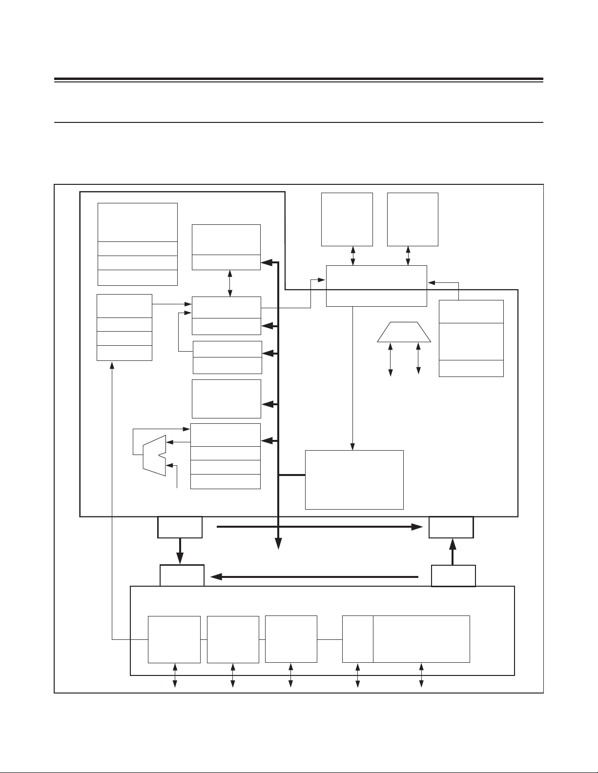
The MAXQ612/MAXQ622 are designed to be modular and expandable. Top-level instruction decoding is extremely
simple and based on transfers to and from registers. The registers are organized into functional modules, which are
in turn divided into the system register and peripheral register groups. Figure 2-1 illustrates the modular architecture
and the basic transport possibilities.
CLOCK CONTROL,
WATCHDOG TIMER
AND POWER MONITOR
CKCN
WDCN
IC
INTERRUPT
LOGIC
IC
IV
IPR0
STACK
MEMORY
SP
ADDRESS
GENERATION
IP
LOOP COUNTERS
LC[
n]
BOOLEAN
VARIABLE
MANIPULATION
ACCUMULATORS
(16)
AP
APC
PSF
PROGRAM
MEMORY
MEMORY MANAGEMENT
UNIT (MMU)
INSTRUCTION
DECODE
(src, dst TRANSPORT
DETERMINATION)
DATA
MEMORY
SC
MUX
SYSTEM MODULES/
REGISTERS
DATA POINTERS
DP[0], DP[1]
FP =
(BP + OFFS)
DPC
src
dst
dst
src
PERIPHERAL MODULES/REGISTERS
USART,
SPI,
2
C
I
TIMERS/
COUNTERS
Figure 2-1. MAXQ612/MAXQ622 Transport-Triggered Architecture
Maxim Integrated 2-3
GENERAL-
PURPOSE
I/O
USB
ADDITIONAL MODULES
FOR FUTURE EXPANSION
Page 8

MAXQ612/MAXQ622 User’s Guide
Memory access from the MAXQ612/MAXQ622 is based on a Harvard architecture with separate address spaces
for program and data memory. The simple instruction set and transport-triggered architecture allow the MAXQ612/
MAXQ622 to decode and execute nearly all instructions in a single clock cycle. Data memory is accessed through one
of three data pointer registers. Two of these data pointers, DP[0] and DP[1], are stand-alone 16-bit pointers. The third
data pointer, FP, is composed of a 16-bit base pointer (BP) and an offset register (OFFS). All three pointers support
postincrement/decrement functionality for read operations and preincrement/decrement for write operations. For the
frame pointer (FP = BP[OFFS]), the increment/decrement operation is executed on the OFFS register and does not
affect the base pointer (BP). Stack functionality is accessible through the stack pointer (SP). Program memory is read
accessible through the code pointer (CP), which supports postincrement/decrement functionality.
2.1 Instruction Decoding
Every MAXQ instruction is encoded as a single 16-bit word according to the format shown in Figure 2-2.
format Destination source
f d d d d d d d s s s s s s s s
Figure 2-2. Instruction Word Format
Bit 15 (f) indicates the format for the source field of the instruction as follows:
• If f equals 0, the instruction is an immediate source instruction, and the source field represents an immediate 8-bit
value.
• If f equals 1, the instruction is a register source instruction, and the source field represents the register from which
the source value is read.
Bits 0 to 7 (ssssssss) represent the source for the transfer. Depending on the value of the format field, this can either
be an immediate value or a source register. If this field represents a register, the lower 4 bits contain the module specifier and the upper 4 bits contain the register index in that module.
Bits 8 to 14 (ddddddd) represent the destination for the transfer. This value always represents a destination register,
with the lower 4 bits containing the module specifier and the upper 3 bits containing the register subindex within that
module.
Because the source field is 8 bits wide and 4 bits are required to specify the module, any one of 16 registers in that
module can be specified as a source. However, the destination field has one less bit, which means that only eight
registers in a module can be specified as a destination in a single-cycle instruction.
While the asymmetry between source and destination fields of the op code can initially be considered a limitation, this
space can be used effectively. First, since read-only registers can never be specified as destinations, they can be
placed in the second eight locations in a module to give single-cycle read access. Second, there are often critical control or configuration bits associated with system and certain peripheral modules where limited write access is beneficial
(e.g., watchdog timer enable and reset bits). By placing such bits in one of the upper 24 registers of a module, this
write protection is added in a way that is virtually transparent to the assembly source code. Anytime that it is necessary
to directly select one of the upper 24 registers as a destination, the prefix register, PFX[n], is used to supply the extra
destination bits. This prefix register write is inserted automatically by the assembler/compiler and requires one
additional execution cycle.
The MAXQ architecture is transport-triggered. This means that writing to or reading from certain register locations also
causes side effects. These side effects form the basis for the higher level op codes defined by the assembler, such
as ADDC, OR, JUMP, and so on. These op codes are actually implemented as MOVE instructions between certain
register locations, while the encoding is handled by the assembler/compiler and need not be a concern to the
programmer. The registers defined in the system register and peripheral register maps operate as described in the
documentation; the unused empty locations are the ones used for these special cases.
2-4 Maxim Integrated
Page 9

MAXQ612/MAXQ622 User’s Guide
The MAXQ instruction set is designed to be highly orthogonal. All arithmetic and logical operations that use two registers can use any register along with the accumulator. Data can be transferred between any two registers in a single
instruction.
2.2 Register Space
The MAXQ612/MAXQ622 provide a total of 16 register modules. Each of these modules contains 32 registers. The first
eight registers in each module can be read from or written to in a single cycle; the second eight registers can be read
from in a single cycle and written to in two cycles (by using the prefix register, PFX[n]); the last 16 registers can be
read or written in two cycles (always requiring use of the prefix register, PFX[n]).
Registers can be either 8 or 16 bits in length. Within a register, any number of bits can be implemented; bits not
implemented are fixed at zero. Data transfers between registers of different sizes are handled as shown in Table 2-1.
• If the source and destination registers are both 8 bits wide, data is transferred bit to bit accordingly.
• If the source register is 8 bits wide and the destination register is 16 bits wide, the data from the source register is
transferred into the lower 8 bits of the destination register. The upper 8 bits of the destination register are set to the
current value of the prefix register; this value is normally zero, but it can be set to a different value by the previous
instruction if needed. The prefix register reverts back to zero after one cycle, so this must be done by the instruction
immediately before the one that would be using the value.
• If the source register is 16 bits wide and the destination register is 8 bits wide, the lower 8 bits of the source are
transferred to the destination register.
• If both registers are 16 bits wide, data is copied bit to bit.
The above rules apply to all data movements between defined registers. Data transfer to/from undefined register locations has the following behavior:
• If the destination is an undefined register, the MOVE is a dummy operation, but can trigger an underlying operation
according to the source register (e.g., @DP[n]--).
• If the destination is a defined register and the source is undefined, the source data for the transfer depends upon the
source module width. If the source is from a module containing 8-bit or 8-bit and 16-bit source registers, the source
data is equal to the prefix data concatenated with 00h. If the source is from a module containing only 16-bit source
registers, 0000h source data is used for the transfer.
The 16 available register modules are broken up into two different groups. The low six modules (specifiers 0h to5h) are
known as the peripheral register modules, while the high 10 modules (specifiers 6h to 0Fh) are known as the system
register modules. These groupings are descriptive only, as there is no difference between accessing the two register
groups from a programming perspective.
The system registers define basic functionality that remains the same across all products based on the MAXQ612/
MAXQ622 architecture. This includes all register locations that are used to implement higher level op codes as well as
the following common system features:
• ALU (16 bits) and associated status flags (zero, equals, carry, sign, overflow)
• 16 working accumulator registers (16-bit width), along with associated control registers
• Instruction pointer
• Registers for interrupt control and handling
• Autodecrementing loop counters for fast, compact looping
• Two data pointer registers, a frame pointer, and a stack pointer for data memory/stack access
• One code pointer register for program memory access
The peripheral registers define additional functionality included in the MAXQ612/MAXQ622. This functionality is broken
up into discrete modules so that only the features that are required for a given product need to be included. Because
the peripheral registers add functionality outside the common MAXQ system architecture, they are not used to implement op codes.
Maxim Integrated 2-5
Page 10

MAXQ612/MAXQ622 User’s Guide
Table 2-1. Register-to-Register Transfer Operations
SOURCE REGISTER
SIZE (BITS)
8 8 — Source[7:0]
8 16 No 00h Source[7:0]
8 16 Yes Prefix[7:0] Source[7:0]
16 8 — Source[7:0]
16 16 No Source[15:8] Source[7:0]
DESTINATION
REGISTER SIZE
(BITS)
PREFIX SET?
DESTINATION SET TO VALUE
HIGH 8 BITS LOW 8 BITS
2.3 Memory Organization
Beyond the internal register space, memory on the MAXQ612/MAXQ622 microcontrollers is organized according to a
Harvard architecture, with a separate address space and bus for program memory and data memory.
To provide additional memory map flexibility, program memory space can be made accessible as data space, allowing
access to constant data stored in program memory.
2.3.1 Program Memory
Program memory begins at address 0000h and is contiguous through FFFFh (128KB). Program memory is accessed
directly by the program fetching unit and is addressed by the instruction pointer register. From an implementation
perspective, system interrupts and branching instructions simply change the contents of the instruction pointer and
force the op code fetch from a new program location. The instruction pointer is direct read/write accessible by the user
software; write access to the instruction pointer forces program flow to the new address on the next cycle following
the write. The content of the instruction pointer is incremented by one automatically after each fetch operation. The
instruction pointer defaults to 8000h, which is the starting address of the utility ROM. The default IP setting of 8000h is
assigned to allow initial in-system programming to be accomplished with utility ROM code assistance. The utility ROM
code interrogates a specific register bit in order to decide whether to execute in-system programming or jump immediately to user code starting at 0000h. The user code reset vector is stored in the lowest bytes of the program memory.
Program flash memory provides in-system programming capability, but requires that the memory targeted for the write
operation be programmed (erased). The utility ROM provides routines to carry out the necessary operations (erase,
write, verify) on flash memory.
2.3.2 Utility ROM
A utility ROM is placed in the start of the upper half of the program memory space starting at address 8000h. This utility
ROM provides the following system utility functions:
• Reset vector
• Bootstrap function for system initialization
• Utility functions to match/query customer specific secrets to prevent loading and/or operation on generic MAXQ612/
MAXQ622 parts
• In-application programming (flash versions only)
• In-circuit debug (flash versions only)
2-6 Maxim Integrated
Page 11

MAXQ612/MAXQ622 User’s Guide
Following each reset, the processor automatically starts execution at address 8000h in the utility ROM, allowing utility
ROM code to perform any necessary system support functions. Next, the SPE bit is examined to determine whether
system programming should commence or whether that code should be bypassed, instead forcing execution to vector
to the start of user program code. When the SPE bit is set to 1, the processor executes the prescribed bootstrap-loader
mode program that resides in utility ROM. The SPE bit defaults to 0. To enter the bootstrap loader mode, the SPE bit
can be set to 1 during reset by the JTAG interface. When in-system programming is complete, the bootstrap loader
can clear the SPE bit and reset the device such that the in-system programming routine is subsequently bypassed.
2.3.3 Data Memory
On-chip SRAM data memory begins at address 0000h and is contiguous through 0BFFh (6KB) in word mode. Data
memory is accessed by indirect register addressing through a data pointer (@DP), frame pointer (@BP[OFFS]), or
stack pointer (PUSH/POP). The data pointer is used as one of the operands in a MOVE instruction. If the data pointer is
used as source, the CPU performs a load operation that reads data from the data memory location addressed by the
data pointer. If the data pointer is used as destination, the CPU executes a store operation that writes data to the data
memory location addressed by the data pointer. The data pointer itself can be directly accessed by the user software.
The MAXQ612/MAXQ622 incorporate two 16-bit data pointers (DP[0] and DP[1]) to support data block transfers. All
data pointers support indirect addressing mode and indirect addressing with autoincrement or autodecrement. Data
pointers DP[0] and DP[1] can be used as postincrement/decrement source pointers by a MOVE instruction or preincrement/decrement destination pointers by a MOVE instruction. Using a data pointer indirectly with “++” automatically
increases the content of the active data pointer by 1 immediately following the execution of read data transfer (@
DP[n]++) or immediately preceding the execution of a write operation (@++DP[n]). Using data pointer indirectly with
“--” decreases the content of the active data pointer by 1 immediately following the execution of read data transfer (@
DP[n]--) or immediately preceding the execution of a write operation (@--DP[n]).
The frame pointer (BP[OFFS]) is formed by 16-bit unsigned addition of frame pointer base register (BP) and frame
pointer offset register (OFFS). Frame pointer can be used as a postincrement/decrement source pointer by a MOVE
instruction or as a preincrement/decrement destination pointer. Using the frame pointer indirectly with “++” (@
BP[++OFFS] for a write or @BP[OFFS++] for a read) automatically increases the content of the frame pointer offset
by 1 immediately before or after the execution of data transfer depending upon whether it is used as a destination or
source pointer respectively. Using frame pointer indirectly with “--” (@BP[--OFFS] for a write or @BP[OFFS--] for a read)
decreases the content of the frame pointer offset by 1 immediately before/after execution of data transfer depending
upon whether it is used as a destination or source pointer, respectively. Note that the increment/decrement function
affects the content of the OFFS register only, while the contents of the BP register remain unaffected by the borrow/
carryout from the OFFS register.
In addition, the MAXQ612/MAXQ622 have a code pointer (CP) to support data block transfer from flash memory. This
allows the user to access the program flash memory as data, even when execuing from the flash. In addition, there
are some restrictions on the use of the code pointer due to memory access protection. See 2.6.3 Memory Access
Protection Impact on Data Pointers (and Code Pointer) for details. The code pointer, like the normal data pointers,
supports indirect addressing mode and indirect addressing with autoincrement or autodecrement. The code pointer
can be used as postincrement/decrement source pointer by MOVE instructions. Using the code pointer indirectly with
“++” automatically increases the content of the active code pointer by 1 immediately following the execution of the read
operation (e.g., MOVE dst, @CP++). Using code pointer indirectly with “--” decreases the content of the active code
pointer by 1 immediately following the execution of the read operation (e.g., MOVE dst, @CP--).
A normal data memory cycle using DP[0], DP[1], and FP to access SRAM takes only one system clock period to support fast internal execution. This allows read or write operations on SRAM to be completed in one clock cycle. To read
program memory as data using CP requires two system clocks. Data memory mapping and access control are handled
by the memory management unit (MMU). Read/write access to the data memory can be in word or in byte.
Maxim Integrated 2-7
Page 12

MAXQ612/MAXQ622 User’s Guide
2.3.4 Stack Memory
The MAXQ612/MAXQ622 implement a soft stack that uses the on-chip data memory (SRAM) for storage of program
return addresses and general-purpose use. The stack is used automatically by the processor when the CALL, RET, and
RETI instructions are executed and when an interrupt is serviced; it can also be used explicitly to store and retrieve data
by using the PUSH, POP, and POPI instructions. The POPI instruction acts identically to the POP instruction, except
that it additionally set the IPS bits.
The width of the stack is 16 bits to accommodate the instruction pointer size. As the stack pointer register, SP, is used
to hold the index of the top of the stack, the maximum size of the stack allowed for a MAXQ612/MAXQ622 is the SRAM
data memory size.
On reset, the stack pointer SP initializes to the top of the stack (03F0h). The CALL, PUSH, and interrupt vectoring
operations increase the stack depth (decrement SP) and then store a value at the memory location pointed to by SP.
The RET, RETI, POP, and POPI operations retrieve the value at @SP and then decrease the stack depth (increment SP).
2.4 Memory Management Unit
Memory allocation and access control for program and data memory is managed by the MMU.
The MAXQ612/MAXQ622 MMU supports the following:
• Flash code memory of up to 128KB; utility ROM of 6KB and data memory SRAM of 6KB.
• In-system and in-application programming of embedded flash (flash versions only).
• Access to any of the three memory areas (SRAM, code memory, utility ROM) using the data memory pointers and
the code pointer.
• Execution from any of the program memory areas (code memory, factory written and tested utility ROM routines)
and from data memory.
Given the above capabilities, the following rules apply to the memory map:
• Program memory:
Physical program memory pages (P0, P1, P2, P3) are logically mapped into data space based upon selection of
byte/word access mode and CDA[1:0] bit settings.
• Data memory:
Access can be either word or byte.
All 16 data pointer address bits are significant in either access mode (word or byte).
The MAXQ612/MAXQ622 can merge program and data into a linear memory map. This is accomplished by mapping
the data memory into the program space or mapping program memory segment into the data space.
2.5 Memory Mapping
Figure 2-3 summarizes the MAXQ612/MAXQ622 default memory maps.
2-8 Maxim Integrated
Page 13

MAXQ612/MAXQ622 User’s Guide
PROGRAM
SPACE
88FFh
3K x 16
UTILITY ROM
8000h
FFFFh
64K x 16
PROGRAM FLASH
0000h
DATA SPACE
(BYTE MODE)
17FFh
x 8
DATA SRAM
0000h
Figure 2-3. MAXQ612/MAXQ622 Memory Map (64KB Program Space)
Table 2-2. CDA Bits to Access Program Space as Data
DATA SPACE
(WORD MODE)
08FFh
x 16
DATA SRAM
0000h
CDA[1:0] SELECTED PAGE IN BYTE MODE SELECTED PAGE IN WORD MODE
00 P0 P0 and P1
01 P1 P0 and P1
10 P2 P2 and P3
11 P3 P2 and P3
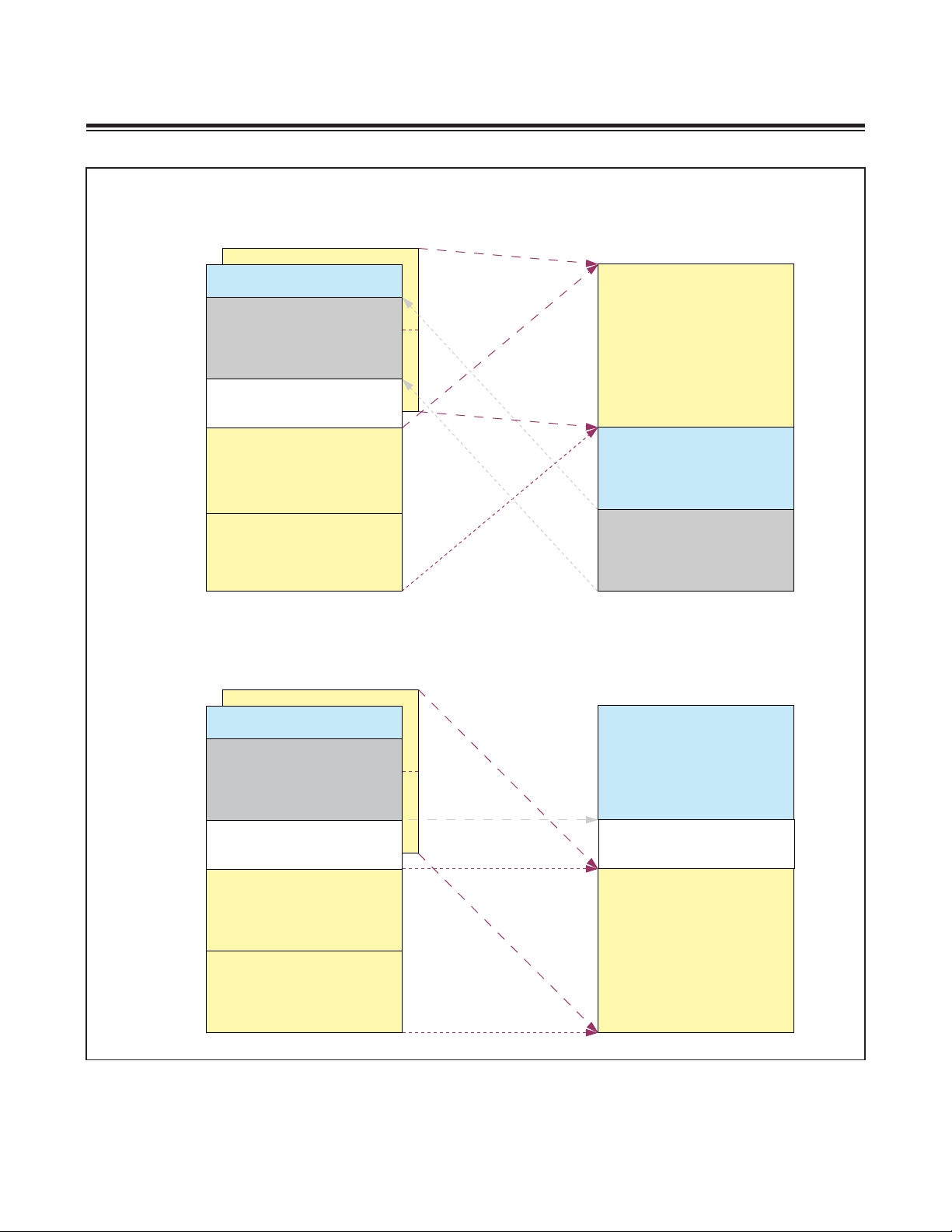
2.5.1 Memory Mapping Into Data Space
The MAXQ612/MAXQ622 map program memory into data space from 0000h to FFFFh. The selection of physical program memory page or pages to be logically mapped to data space is determined by the CDA1 and CDA0 bits, as
shown in Table 2-2.
Figure 2-3 summarize the default memory maps for this memory structure. The WBSn bits of the MAXQ612/MAXQ622
default to word access mode (WBSn = 1).
The upper half of the data memory map (8000h to FFFFh) is the logical area for the utility ROM when accessed as
data. Executing code from the utility ROM allows the user to map the program memory to 8000h to FFFFh by properly
selecting the CDA bits.
Figure 2-4 and 2-5 illustrate the effects of the CDA bits.
Maxim Integrated 2-9
Page 14
MAXQ612/MAXQ622 User’s Guide
WORD MODE MEMORY MAP (UPA = 0, EXECUTING FROM UTILITY ROM)
PROGRAM MEMORY
15 0
xFFFF
xA000
x8000
x0000
LOGICAL SPACE
UTILITY ROM
PHYSICAL PROGRAM
(P1)
PHYSICAL PROGRAM
(P0)
P3
P2
CDA1 = 1
CDA1 = 0
WORD MODE MEMORY MAP (UPA = 0, EXECUTING FROM PHYSICAL DATA MEMORY)
15 0
xFFFF
LOGICAL SPACE
P3
DATA MEMORY
15
PHYSICAL DATA
DATA MEMORYPROGRAM MEMORY
15
0
x8000
x4000
x0000
0
xFFFF
LOGICAL SPACE
LOGICAL DATA MEMORY
xA000
UTILITY ROM
x8000
PHYSICAL PROGRAM
(P1)
PHYSICAL PROGRAM
(P0)
x0000
P2
LOGICAL UTILITY ROM
x8000
CDA1 = 1
CDA1 = 0
x0000
Figure 2-4. CDA Functions in Word Mode
2-10 Maxim Integrated
Page 15

MAXQ612/MAXQ622 User’s Guide
BYTE MODE MEMORY MAP (EXECUTING FROM UTILITY ROM)
15 0 07
xFFFF
xA000
x8000
x0000
LOGICAL SPACE
UTILITY ROM
PHYSICAL PROGRAM
(P1)
PHYSICAL PROGRAM
(P0)
CDA[1:0] = 00
BYTE MODE MEMORY MAP (EXECUTING FROM PHYSICAL DATA MEMORY)
15 0 07
xFFFF
LOGICAL SPACE
DATA MEMORYPROGRAM MEMORY
xFFFF
x8000
CDA[1:0] = 01
PHYSICAL DATA
x0000
DATA MEMORYPROGRAM MEMORY
xFFFF
LOGICAL SPACE
xA000
UTILITY ROM
x8000
x0000
PHYSICAL PROGRAM
(P1)
PHYSICAL PROGRAM
(P0)
CDA[1:0] = 01
CDA[1:0] = 00
x8000
x0000
Figure 2-5. CDA Functions in Byte Mode
Maxim Integrated 2-11
Page 16
MAXQ612/MAXQ622 User’s Guide
CODE POINTER ACCESS OF WORD MODE MEMORY MAP
CODE POINTER MAPPHYSICAL PROGRAM MEMORY
15 0
xFFFF
PHYSICAL PROGRAM (P3)
15 0
PHYSICAL PROGRAM (P3)
xFFFF
PHYSICAL PROGRAM (P2)
PHYSICAL PROGRAM (P1)
PHYSICAL PROGRAM (P0)
x0000
PHYSICAL PROGRAM (P2)
PHYSICAL PROGRAM (P1)
PHYSICAL PROGRAM (P0)
CODE POINTER OF BYTE MODE MEMORY MAP
PHYSICAL PROGRAM MEMORY
15 0 07
xFFFF
PHYSICAL PROGRAM (P3)
PHYSICAL PROGRAM (P2)
PHYSICAL PROGRAM (P1)
PHYSICAL PROGRAM (P0)
x0000
CPA = 1
CPA = 0
x0000
CODE POINTER MAP
xFFFF
x0000
Figure 2-6. CPA Impact on Code Pointer Access of Program Memory
Table 2-3. CPA Access of Program Data with Code Pointer
CPA BYTE MODE ACCESS WORD MODE ACCESS
0 Lower 64KB Don’t care/no effect
1 Upper 64KB Don’t care/no effect
2.5.2 Memory Mapping into Code Space
The effective program address can be anywhere in the full 128KB memory space. Program memory from 0000h to
FFFFh is the normal user code segment, followed by the utility ROM. The top of the memory is the logical area for data
memory when accessed as a code segment. Pages P2, P3 of the program memory are not accessible for program
execution by default. These pages need to be activated by user software. The upper program access (UPA) bit must
be set to 1 to activate P2 and P3. Once UPA is set, P2 and P3 occupy the upper half of the program space, and utility
ROM and physical data memory can be accessed as data only. Figure 2-7 summarizes UPA effect.
2-12 Maxim Integrated
Page 17
MAXQ612/MAXQ622 User’s Guide
MAXQ612/MAXQ622 MEMORY MAP (DEFAULT, UPA = 0)
PROGRAM MEMORY
15 0
xFFFF
LOGICAL SPACE
P3
DATA MEMORY
15
0
xFFFF
xA000
UTILITY ROM
x8000
PHYSICAL PROGRAM
(P1)
PHYSICAL PROGRAM
(P0)
x0000
MAXQ612/MAXQ622 MEMORY MAP (UPA = 1)
15
xFFFF
x8000
PROGRAM MEMORY
PHYSICAL PROGRAM
(P3)
PHYSICAL PROGRAM
(P2)
P2
x8000
LOGICAL SPACE
x4000
PHYSICAL DATA
x0000
0
15
DATA MEMORY
LOGICAL UTILITY ROM
0
xFFFF
x8000
PHYSICAL PROGRAM
(P1)
PHYSICAL PROGRAM
(P0)
x0000
LOGICAL SPACE
x4000
PHYSICAL DATA
x0000
Figure 2-7. MAXQ622 Memory Map and UPA
Maxim Integrated 2-13
Page 18

MAXQ612/MAXQ622 User’s Guide
2.5.3 Memory Mapping Rules
When executing program code in a particular memory segment, the same memory segment cannot be simultaneously
accessed as data.
The following is a summary of the memory mapping rules.
• When executing from the normal user code segment:
The lower 32KWords program space (P0 and P1) is always executable as program.
The upper half of the code segment (P2 and P3) is accessible as program when UPA is set to 1.
The utility ROM is an extension of the program space if the UPA bit is 0.
The physical data memory is available for access as a code segment with offset at 0A000h if the UPA bit is 0.
Load and store operations to data memory are executed normally when addressed to the physical data memory.
The utility ROM can be read as data, starting at 08000h of the data space.
• When executing from the utility ROM (only when UPA bit is 0):
The lower 32KWords program space (P0 and P1) functions as normal program memory.
Data memory is available for access as a code segment at the upper half of the program memory map, immediately
following the utility ROM segment.
Load and store operations to data memory are executed normally when addressed to the physical data memory.
P0 can be accessed as data with offset at 08000h when CDA[1:0] = 00b in byte mode or CDA1 = 0 in word mode.
P1 can be accessed as data with offset at 08000h when CDA[1:0] = 01b in byte mode or at offset 0C000h when
CDA1 = 0 in word mode.
P2 can be accessed as data with offset at 00000h when CDA[1:0] = 10b in byte mode or CDA1 = 1 in byte mode.
P3 can be accessed as data with offset at 00000h when CDA[1:0] = 11b in byte mode or at offset 0C00h when CDA1
= 1 in word mode.
• When executing from the data memory (only when UPA is 0):
Program flows freely between the lower 32KWords user code (P0 and P1) and the utility ROM segment.
The utility ROM can be accessed as data with offset at 08000h.
P0 can be accessed as data with offset at 0000h when CDA[1:0] = 00b in byte mode or CDA1 = 0 in word mode.
P1 can be accessed as data with offset at 0000h when CDA[1:0] = 01b in byte mode or at offset 04000h when CDA1
= 0 in word mode.
P2 can be accessed as data with offset at 00000h when CDA[1:0] = 10b in byte mode or CDA1 = 1 in byte mode.
P3 can be accessed as data with offset at 00000h when CDA[1:0] = 11b in byte mode or at offset 0C00h when CDA1
= 1 in word mode.
2-14 Maxim Integrated
Page 19

MAXQ612/MAXQ622 User’s Guide
2.5.4 Code Examples
Because the MAXQ622 uses the maximum allowed program flash supported by this core, the most extreme example
of data pointer access would be the final bytes of the flash in byte mode. This can be accomplished by executing from
data memory (requiring the UPA bit to be cleared) and setting the CDA bits to map program segment P3 to the data
memory area. Code to read the final 3 bytes of the flash is shown below. This code would need to be executed from
data memory. Note that it is assumed that memory access protection, system clocking, etc., are all configured to allow
this access.
move SC, #00B0 ; UPA=0, CDA[1:0]=11
move DPC, #0000 ; SDPS[1:0]=00, WBS0=0
move DP[0], #07FFD ;Point to 3 addresses from top of prog mem mapped intodata
move ACC, @DP[0]++ ; Move first byte to ACC to check and post increment
call CHECKB1 ; call subroutine to check first byte
move ACC, @DP[0]++ ; Move second byte to ACC to check and post increment
call CHECKB2
move ACC, @DP[0] ; Move final byte to ACC
call CHECKB3
Alternatively, the code pointer could be used for the same purpose. The advantage of this is that no code loading to
data memory is required and the UPA bit does not affect the operation. Also, the mechanism for accessing the upper
(P3) segment is a little different, using only the CPA bit instead of the CDA bits to access the upper 64KB of program
memory (since the code pointer uses the entire 64K address space for code).
move SC, #0040 ; CPA=1
move DPC, #0000 ; CWBS=0
move CP, #0FFFD ; Point to 3 addresses from very top
move ACC, @CP++ ; Move first byte to ACC to check and post increment
call CHECKB1 ; call subroutine to check first byte
move ACC, @CP++ ; Move second byte to ACC to check and post increment
call CHECKB2
move ACC, @CP ; Move final byte to ACC
call CHECKB3
The above code could be called directly from user code in the program flash; however, each access would require two
system clock cycles to complete as opposed to the usual one cycle for data pointer access.
Maxim Integrated 2-15
Page 20

MAXQ612/MAXQ622 User’s Guide
2.6 Memory Protection
The MAXQ612/MAXQ622 support privilege levels for code. When enabled, code memory is separated into three areas.
Each area has an associated privilege level. RAM/utility ROM are assigned privilege levels as well:
• Code in the system area can be confidential. Code in the user areas can be prevented from reading and writing
system code.
• The user loader can be protected from user application code.
Table 2-4. Memory Areas and Associated Maximum Privilege Levels
AREA PAGE ADDRESS MAXIMUM PRIVILEGE LEVEL
System 0 to ULDR-1 High
User Loader ULDR to UAPP-1 Medium
User Application UAPP to top Low
Utility ROM N/A High
Other (RAM) N/A Low
The PRIV register reflects the current execution privilege. Hardware guarantees that the contents of PRIV are never
higher than the maximum privilege level of the memory area the code is running from. For example, if user code were
trying to set PRIV to high, this would be prevented by hardware. However, any code can decide to lower the privilege
level at any time (see Equation 1).
PRIV = min(maxprivilege(IP), PRIV) (Equation 1)
The bit contents of the PRIV register are shown in Table 2-5. The convenient constants high/medium/low are defined
in Table 2-6, but all values from 00b to 11b can be used.
In addition to the PRIV register, the privilege level can also be set by writing to PRIVT0 and PRIVT1 in sequence. Again,
hardware guarantees that the contents of PRIVT0 are never higher than the maximum privilege level of the memory
area the code is running from.
When writing to PRIVT1, hardware modifies the PRIV register based on Equation 2.
PRIV = min(PRIVT0, argument, maxprivilege(IP)) (Equation 2)
This means that, when using PRIVT[1:0], the privilege level cannot be raised unless all code between the writes to
PRIVT0 and PRIVT1 executes. Writing to PRIV automatically resets PRIVT0 to low.
Table 2-5. PRIV Register Bit Definitions
BIT
MEANING
3 2 1 0
System Write System Read User Loader Write User Loader Read
Table 2-6. Privilege Level Constants
BIT
HIGH
MEDIUM
LOW
In addition to the PRIV register, the privilege level can also be set by writing to PRIVT0 and PRIVT1 in sequence. Again,
hardware guarantees that the contents of PRIVT0 are never higher than the maximum privilege level of the memory
area the code is running from.
When writing to PRIVT1, hardware modifies the PRIV register based on
2-16 Maxim Integrated
3 2 1 0
1 1 1 1
0 0 1 1
0 0 0 0
PRIV’ = min(PRIVT0, argument, maxprivilege(IP))
Page 21

MAXQ612/MAXQ622 User’s Guide
This means that when using PRIVT0/PRIVT1, the privilege level cannot be raised unless all code between the writes to
PRIVT0 and PRIVT1 executes. Writing to PRIV automatically resets PRIVT0 to low.
2.6.1 Rules for System Software
While privilege levels are implemented in hardware, there are two ways user code could try to circumvent the memory
access protection:
• Manipulation of shared, common stack or registers
• Jumping or calling to code in system memory that is not an official entry point
To ensure a safe system and prevent these attacks, the system code programmer must follow the following rules:
• System code must not save and restore the privilege level. Instead, every interrupt and every system library function that raises the privilege must also unconditionally lower the privilege before exiting. If there are interrupts
that lower the privilege level, or interrupt code running outside of system space, any code that raises the privilege
must disable interrupts for the duration of the privileged operation.
Example:
interrupt:
move IGE, #0
move PRIV, #HIGH
… ; action
move PRIV, #LOW
move IGE, #1
reti
system_code:
move IGE, #0
move PRIV, #HIGH
... ; action
move PRIV, #LOW
move IGE, #1
ret
• An operation that requires high privilege levels must not call subroutines to raise the privilege level.
Example:
incorrect:
call raise_priv
… ; action
move PRIV, #LOW
correct:
move PRIV, #HIGH
… ; action
move PRIV, #LOW
Maxim Integrated 2-17
Page 22

MAXQ612/MAXQ622 User’s Guide
• A system library function that checks arguments before raising the privilege level must do so in an atomic fashion using PRIVT0 and PRIVT1 to prevent short-circuiting the check (the rule about disabling interrupts also applies).
Example:
system_library:
move IGE, #0
move PRIVT0, #HIGH
… ; check
jump ne, exit move PRIVT1, #HIGH
; … action
exit:
move PRIV, #LOW
move IGE, #1
ret
2.6.2 Privilege Exception Interrupt
Any attempt to exceed the current privilege level causes a privilege exception interrupt that can be handled by system
code. Examples that cause an interrupt are writing high to PRIV from user code, or trying to read system code while
PRIV is low. The intent of the interrupt is to notify low priority code when an operation was denied by hardware.
2.6.3 Memory Access Protection Impact on Data Pointers (and Code Pointer)
Memory access protection complicates the use of the data and code pointers. In the MAXQ architecture, code pointers
must be activated before use in order for memory data to be available on the same cycle it is needed using synchronous RAMs. This means that data is essentially prefetched into the physical data pointer when the pointer is activated
(e.g., by loading an address to DP[0]). This can have some unintended consequences with respect to the memory
protection function.
Specifically, when MPE is enabled, and when executing from RAM, any write to the traditional MAXQ data pointers,
DP[0], DP[1], and BP, OFFS, or DPC, has the potential to generate a memory fault.
For example, a scenario in which code is executed from RAM is presented. In this particular case, the code is stored in
a serial EEPROM. The code is loaded dynamically into RAM when needed. It is assumed this code has to have access
to RAM variables, and remember we are executing from RAM.
To accomplish this without memory access protection, the customer would configure DPC and load DP[0] and then
call the utility ROM function UROM_moveDP0. The code would look like the following:
MOVE DPC, #REQUIRED_DP0_MODE ; (1)
MOVE DP[0], #REQUESTED_RAM_ADDRESS ; (2)
LCALL UROM_MOVEDP0 ; (3)
; actual ROM function
MOVE DP[0], DP[0] ; (3a)
MOVE GR, @DP[0] ; (3b)
RET ; (3c)
In the above example, (1) and (2) are both considered valid pointer activation instructions. In the MAXQ transfertriggered architecture every standard instruction represents a MOVE from a source (SRC) to a destination (DST). The
POP ACC instruction is equivalent to MOVE ACC, @SP--, JUMP LABEL is equivalent to MOVE IP, #LABEL, and so on.
With the exception of a handful of arithmetic and logical instructions, every instruction is interpreted as a MOVE DST,
SRC operation.
2-18 Maxim Integrated
Page 23

MAXQ612/MAXQ622 User’s Guide
This is no different for instructions that operate on data pointers. For example, a pointer to pointer move such as MOVE
@DP[1], @DP[0] first requires the read pointer to be activated. Architecturally, this strobes the chip enable and read
signals on the memory mapped to the location in DP[0]. This value is latched internally so that it is available when @
DP[0] is used as the source operand. At that time, the internally latched data is transferred to the destination register.
This functions normally when memory protection is not enabled. However if MPE is set the same code can cause a
memory protection fault. For this example let us assume the following:
1) The code is executing from RAM
2) REQUESTED_RAM_ADDRESS is defined as #0000h
3) Flash memory is located from 0000h–7FFFh
MOVE DPC, #REQUIRED_DP0_MODE ; Activates DP[0]
; In this MMU mapping,
; addresses 0-7FFFh are in Flash
; and *if* the previous contents
; of DP[0], modified by DPC, are
; in System space, we will generate
; a memory fault
MOVE DP[0], #REQUESTED_RAM_ADDRESS ; Again, activates DP[0]
; Now we know that DP[0]
; points to address 0000h
; and in the current MMU
; mapping, we are
; definitely pointing to
; *and reading from*
; System space in flash.
; MEMORY FAULT GUARANTEED
LCALL UROM_MOVEDP0 ; Changes MMU mapping. In
; this case, addresses
; 0-7FFFh point to RAM
; actual ROM function
MOVE DP[0], DP[0] ; ACTIVATE DP[0] in RAM
; space. If we studied
; the above discussion
; carefully, we know that
; *activate* means *read*
MOVE GR, @DP[0] ; Transfer the latched
; DP[0] value to GR
RET ;
So, if MPE is enabled and the memory fault interrupt is enabled, the first two instructions generate a memory fault and
the corresponding interrupt is executed. To avoid a memory fault under these circumstances, a function must be written in flash. This function has to take as an input, the address to be accessed, but it must be passed using a nonpointer
register (such as an accumulator register). The RAM code routine would write the address into this register (e.g., A[0]).
Maxim Integrated 2-19
Page 24

MAXQ612/MAXQ622 User’s Guide
Next, the RAM routine calls into the flash function. Once we are executing out of flash, we can activate the DP[0] pointer
without causing a memory fault because the MMU now maps RAM into address range 0–7FFFh and ROM to higher
addresses. None of this space is MPE protected. That flash routine would look similar to this:
// this routine must be implemented in flash
ReadRAM:
push DPC
move DPC, #18h
move DP[0], A[0]
move A[0] @DP[0]
pop DPC
ret
The corresponding RAM routine looks like:
;
; No pointer activation from RAM code
;
MOVE A[0], #REQUESTED_RAM_ADDRESS
LCALL ReadRAM
2.6.4 Debugging
Note that debugging system code (including trace, break, memory dump, etc.) is disabled once memory protection
is enabled.
2.6.5 Enabling Memory Protection
Memory protection is always enabled unless the system password is empty. Utility ROM initialization code is responsible for checking the password and clearing the memory protection enable (MPE) bit.
2.6.6 Reset Procedure and Setup of Memory Protection
Utility ROM code as well as system and user loader code is responsible for setting up the memory protection boundaries.
Both passwords and memory area boundary definitions are loaded from code memory. These values are part of the system, user loader, and user application image files, and are defined when assembling or compiling the code image files.
Example for the System Image:
org 0000h
; Reset
move CP, #usr_ldr_page
move ULDR, @CP
jump sys_init
org 000Fh
user_ldr_page:
; Starting page address of user loader
dw 0020h ; Page 32
org 0010h
; System password
dw …, …, …, …
org 0020h
interrupt0:
2-20 Maxim Integrated
Page 25
MAXQ612/MAXQ622 User’s Guide
TOP (128KB)
APPL
USR APP PASSWORD
USR LDR PASSWORD
STARTUP
SYS PASSWORD
STARTUP
USR APP START
IVT IVT IVT
IVT IVT IVT
USR LDR START
UAPP
ULDR
0000
LDR
USER
SYSTEMUSER
+10h
+10h
20h
10h
RESET/STARTUP DEBUG LOCK
Figure 2-8. Overview of Memory Regions
Figure 2-8 shows the code memory with passwords and the location of the values that are programmed into the ULDR/
UAPP registers.
The user loader starting page address is located at 0Fh, one word before the system password. The user application
starting page address is stored one word before the user loader password (i.e., ULDR*Flash page size + 0Fh).
The startup sequence is as follows:
1) The system resets at 8000h and starts running utility ROM code. On a 64KB part with flash pages of 512 bytes,
ULDR and UAPP are at their reset values of 80h (end of flash memory). The PRIV register is at its reset value of
high. The MPE (memory protection enable bit) is at its reset value of 1 (enable).
2) Utility ROM initialization code checks the system password and disables MPE if the password is empty.
3) After utility ROM initialization is complete, the utility ROM passes execution to system code memory at address
0000h.
4) System code starts executing and uses a CP of 0Fh to read the user loader starting page address and writes it into
the ULDR register.
5) After system initialization is complete, system code jumps to address ULDR*Flash page size + 0000h. This jump
automatically drops PRIV to medium.
6) The user-loader code starts executing and uses a CP of ULDR*Flash page size + 0Fh to read the user application
starting page address and writes it into the UAPP register.
7) After user loader initialization is complete, user-loader code jumps to address UAPP*Flash page size + 0000h. This
jump automatically drops PRIV to low.
Maxim Integrated 2-21
Page 26

MAXQ612/MAXQ622 User’s Guide
2.6.7 Loader Access Control
As stated previously, the MAXQ612/MAXQ622 have three memory regions: system, user loader, and application. The
loader maintains a context register to determine which of the regions is to be the target of the loader commands. Family
0 and Family F commands have no context. They are global in scope. For details on the nonparty-specific loader commands, refer to Application Note 4012: Implementing a JTAG Bootloader Master for the MAXQ2000 Microcontroller.
There are two Family F loader commands specific to the MAXQ612/MAXQ622:
Command 0xF0: GetContext
Input : None
Output : Context Byte – 00x00, SystemContext; 0x01, LoaderContext; 0x2, ApplicationContext
Command 0xF1” SetContext
Input : Context Byte – 0x00, SystemContext; 0x01, LoaderContext; 0x02, ApplicationContext
Output : Sets Error Code (retrieved using Getstatus bootloader command)
The bootloader sets a default context based on the lowest privileged region that exists. The default context is selected
according to the following rules:
If all three regions exist:
The user application context (UAPP_CONTEXT).
If only system and user application regions exist:
The user application context.
If only system and user loader regions exist:
The user loader context (ULDR_CONTEXT).
If only the system region exists:
The system context (SYSTEM)CONTEXT). Only the default context will have its password tested and
corresponding PWL bit cleared. The context can be changed through the Family F commands shown above, but the
password for the new region is not tested after a context change and, therefore, a password match loader command
must be sent to clear the password lock bit of the associated region even if the password for that region is clear.
If the system password has not been set, memory protection is disabled by the ROM. If word address 000Eh in the
system code region is programmed (any value other than 0xFFFF), the debug lockout condition is set by setting
SC.DBGLCK to 1 (all debug functions are disabled).
The “current context” is used by the loader to determine how to apply master erase and password-protected loader
commands. The master erase command erases pages starting at the base address of the current context and all
pages with addresses greater than the base address. Password-protected commands check the password lock bit of
the current region. The unlock password command uses the password from the current region (indicated by the current
context) to determine the state of the current region password lock.
The loader provides several commands that require a password and a master erase command that does not.
All password-protected commands check the following:
• System password match: Access to full memory
• Loader password match: Access to user memory
• Application password match: Access to user application memory
• No match: No access
Three PWL bits allow the loader to find out whether a password match was successful. The PWL bits for system and
user loader can only be written by utility ROM code (see Section 15.2 Password-Protected Access).
Master erase does not require a password and defaults to erasing the user application only. Two Family F commands
are added that allow master erase of user loader and system code:
• Master erase system: Complete system erase.
• Master erase user loader: Erases user loader and user application.
2-22 Maxim Integrated
Page 27

MAXQ612/MAXQ622 User’s Guide
2.6.8 Disabling MAXQ612/MAXQ622-Specific Memory Access Features
The MAXQ612/MAXQ622 memory-protection features are specific to the MAXQ612/MAXQ622 family of parts and can
cause some confusion in the way that they impact debugging and bootloader commands when compared to MAXQ
parts. To enable users to develop initial firmware as quickly as possible, the following code can be added to your
application code to disable the memory protection features and allow code loading and debugging in the same manner as previous parts:
ORG 0
Jump Start
ORG 000eh
Debug_Lockout:
DW 0ffffh ; disable debug lockout
ORG 000fh
ULDR_PageNumber:
DW 0ffffh ; do not define a user loader page
ORG 0010h
System_PassworD:
DW offffh,offffh, offffh,offffh, offffh,offffh, offffh,offffh
DW offffh,offffh, offffh,offffh, offffh,offffh, offffh,offffh
ORG 0020h
; interrupt vectors go here
ORG 0100h
Start:
; Your application code here
;…
END
Once the memory-protection features are fully understood, this code can be removed from the user’s application code
to enable memory access control.
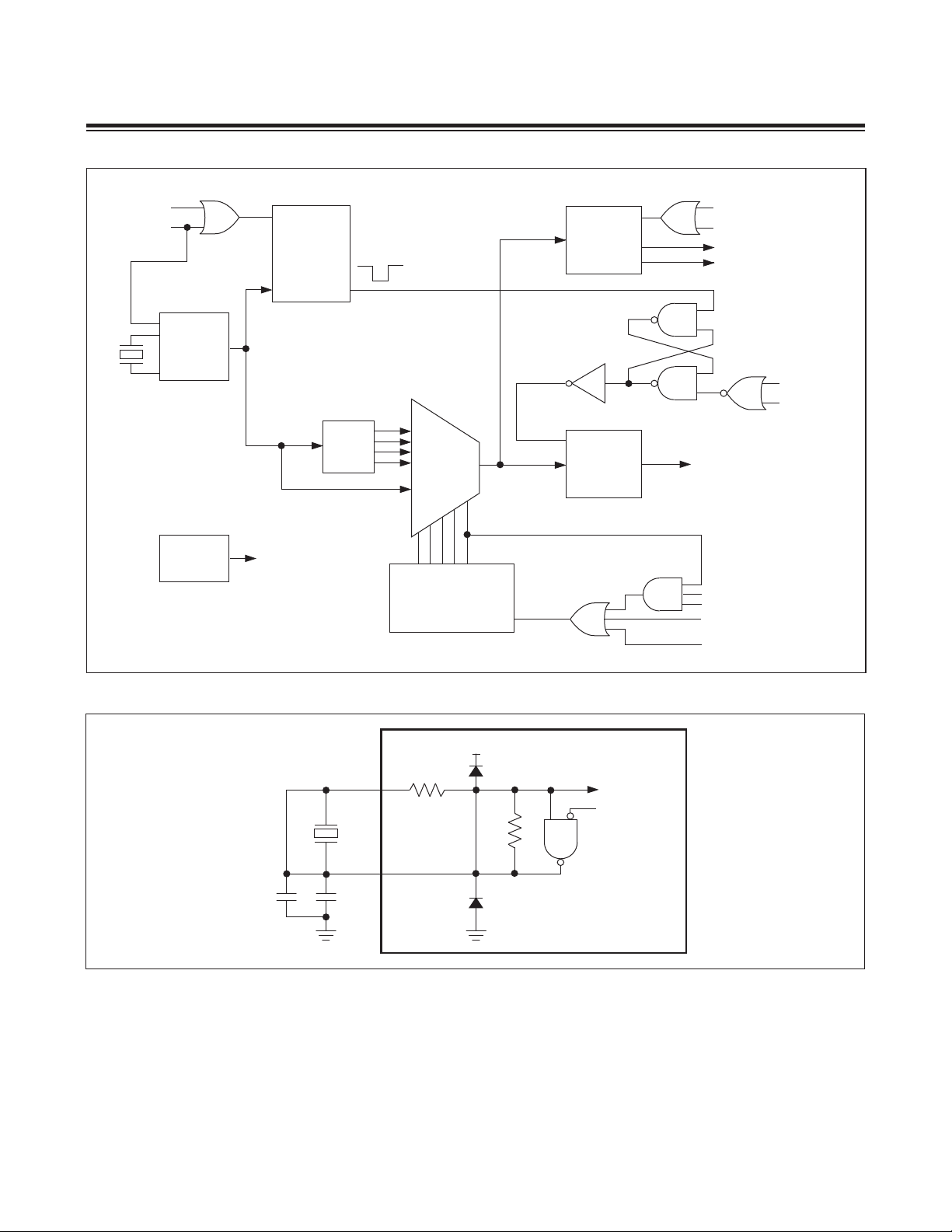
2.7 Clock Generation
All functional modules in the MAXQ612/MAXQ622 are synchronized to a single system clock with the exception of the
wake-up timer. The internal clock circuitry generates the system clock from one of two possible sources:
• Internal oscillator, using an external crystal or resonator
• External clock signal
The external clock and crystal are mutually exclusive since they are input through the same clock pin. Each time code
execution must start or restart (as can be the case when exiting stop mode) using the external clock source, the following sequence occurs:
• Reset the crystal warmup counter.
• Allow the required warmup delay: 8192 external clock cycles if exiting from stop mode.
• Code execution starts after the crystal warmup sequence.
2.7.1 External Clock (Crystal/Resonator)
An external quartz crystal or a ceramic resonator can be connected from HFXIN to HFXOUT determining the frequency,
as illustrated in Figure 2-10. The fundamental mode of the crystal operates as inductive reactance in parallel resonance
with external capacitance to the crystal.
Maxim Integrated 2-23
Page 28
MAXQ612/MAXQ622 User’s Guide
POWER-ON
RESET
STOP
CRYSTAL KILL
HF
CRYSTAL
8kHz
RING
RESET
XDOG
STARTUP
TIMER
CLK INPUT
WAKE-UP TIMER
MAXQ612
MAXQ622
CLOCK
DIVIDER
XDOG DONE
GLITCH-FREE
DIV 1
DIV 2
SELECTOR
DIV 4
MUX
DIV 8
PMM
DEFAULT
RESET DOG
WATCHDOG
TIMER
ENABLE
CLOCK
GENERATION
RWT
RESET
WATCHDOG RESET
WATCHDOG INTERRUPT
SYSTEM CLOCK
SWB
INTERRUPT/SERIAL PORT
RESET
STOP
STOP
POWER-ON
RESET
Figure 2-9. MAXQ612/MAXQ622 Clock Sources
HFXIN
HFXOUT
C1
C2
Figure 2-10. On-Chip Crystal Oscillator
V
DD
R
F
R
= 1MΩ ±50%
F
CLOCK CIRCUITRY
STOP
MAXQ612
MAXQ622
2-24 Maxim Integrated
Page 29

MAXQ612/MAXQ622 User’s Guide
Crystal specifications, operating temperature, operating voltage, and parasitic capacitance must be considered when
designing the internal oscillator. The MAXQ612/MAXQ622 are designed to operate at a 12MHz maximum frequency.
To further reduce the effects of external noise, a guard ring can be placed around the oscillator circuitry.
Pins HFXIN and HFXOUT are protected by clamping devices against on-chip electrostatic discharge. These clamping
devices are diodes parasitic to the feedback resistor RF in the oscillator’s inverter circuit. The inverter circuit is presented as a NAND gate that can disable clock generation in stop mode.
Noise at HFXIN and HFXOUT can adversely affect on-chip clock timing. It is good design practice to place the crystal
and capacitors near the oscillator circuitry and connect to HFXIN, HFXOUT, and ground with a direct shot trace. The
typical values of external capacitors vary with the type of crystal used and should be initially selected based on the
load capacitance as suggested by the crystal manufacturer.
For cost-sensitive applications, a ceramic resonator can be used instead of a crystal. Using the ceramic resonator can
require a different circuit configuration and capacitance value.
2.7.2 External Clock (Direct Input)
The MAXQ612/MAXQ622 CPU can also obtain the system clock signal directly from an external clock source. In this
configuration, the clock generation circuitry is driven directly by an external clock.
To operate the MAXQ612/MAXQ622 from an external clock, connect the clock source to HFXIN and connect HFXOUT
to GND. The clock source should be driven through a CMOS driver. If the clock driver is a TTL gate, its output must
be connected to VDD through a pullup resistor to ensure a satisfactory logic level for active clock pulses. To minimize
system noise on the clock circuitry, the external clock source must meet the maximum rise and fall times and the minimum high and low times specified for the clock source. The external noise can affect clock generation circuit if these
parameters do not meet the specification.
2.7.3 Internal System Clock Generation
The internal system clock is derived from the currently selected oscillator input. By default, one system clock cycle is
generated per oscillator cycle, but the number of oscillator cycles per system clock can also be increased by setting
the power-management mode enable (PMME) bit and the clock-divide control (CD[1:0]) register bits according to
Table 2-7.
Table 2-7. System Clock Rate Control Settings
PMME CD[1:0] CYCLES PER CLOCK
0 00 1 (default)
0 01 2
0 10 4
0 11 8
1 xx 256
2.8 Wake-Up Timer
The MAXQ612/MAXQ622 provide a simple wake-up timer that can trigger an interrupt after a user-definable number of
internal 8kHz ring cycles. Since the wake-up timer is running off the internal ring and keeps running even during stop
mode, it can be used to wake the MAXQ612/MAXQ622 up from stop mode at periodic intervals.
To use the wake-up timer, the WUT register should be written first (before the wake-up timer is started) to define the
countdown interval. Once the time interval has been defined, the wake-up timer can be started by setting the WTE bit
to 1. The time interval until the wake-up timer counts down to zero is defined by:
f
x WUT[15:0]
NANO
With the maximum possible time interval being:
f
x (216 - 1)
NANO
Maxim Integrated 2-25
Page 30

MAXQ612/MAXQ622 User’s Guide
2.8.1 Using the Wake-Up Timer to Exit Stop Mode
To use the wake-up timer to exit stop mode after a predefined period of time, the following conditions must be met
before entering stop mode:
• The WUT register must be written to define the countdown interval value.
• The WTE bit must be written to 1 to start the wake-up timer.
• The IGE (IC.0) bit must be set to 1 to enable global interrupts. The wake-up timer cannot wake the MAXQ612/
MAXQ622 up from stop mode if its interrupt does not fire.
2.9 Interrupts
The MAXQ612/MAXQ622 provide a hardware interrupt handler with interrupt vector (IV) table base address register
and the interrupt control (IC) register. The IV register is fixed at 0020h and acts as the vector table base location.
Interrupts can be generated from system level sources (e.g., watchdog timer) or by sources associated the peripheral
modules. The interrupt vectors are preset at eight fixed memory address offsets from IV with hardware priority control
that can be programmed through the interrupt priority register zero (IPR0 and IPR1).
2.9.1 Servicing Interrupts
For the MAXQ612/MAXQ622 to service an interrupt, interrupt handling must be enabled globally and locally. The IGE
bit located in the IC register acts as a global interrupt mask that affects all interrupts, with the exception of the powerfail warning interrupt. This bit defaults to 0, and it must be set to 1 before any interrupt handling takes place.
The local interrupt-enable bit for a particular source is in one of the peripheral registers associated with that peripheral
module or in a system register for any system interrupt source. When an interrupt condition occurs, its individual flag
is set, even if the interrupt source is disabled at the local or global level. Interrupt flags must be cleared within the user
interrupt routine to avoid repeated interrupts from the same source.
The handler uses three levels of interrupt priorities that allow the user software to select a suitable priority for an interrupt vector source. The interrupt handler (hardware) modifies the interrupt priority status bits (IPSn) when it is servicing
an interrupt. These bits are set to 11b by the interrupt handler when executing a RETI instruction.
2.9.2 Interrupt System Operation
The interrupt handler responds to any interrupt event when it is enabled. An interrupt event occurs when an interrupt
flag is set. All interrupt requests are sampled at the rising edge of the clock, and can be served by the processor one
clock cycle later, assuming the request does not hit the interrupt exception window. The one cycle stall between detection and acknowledgement/servicing is due to the fact that the current instruction could also be accessing the stack,
or that the current instruction could be a prefix register (PFX[n]) write. For this reason, the CPU must allow the current
instruction to complete before pushing the stack and vectoring to the proper interrupt vector table address. If an interrupt exception window is generated by the currently executing instruction, the following instruction must be executed,
thus the interrupt service routine is delayed an additional cycle.
Interrupt operation in the MAXQ612/MAXQ622 CPU is essentially a state-machine-generated long CALL instruction. When the interrupt handler services an interrupt, it temporarily takes control of the CPU to perform the following
sequence of actions:
1) The next instruction fetch from program memory is cancelled.
2) The return address is pushed on to the stack.
3) The IPS bits are set to the current interrupt level to prevent recursive interrupt calls from interrupts of lower priority.
4) The instruction pointer is set to the location of the interrupt service routine as defined by the interrupt source.
5) The CPU begins executing the interrupt service routine.
Once the interrupt service routine completes, it should use the RETI instruction to return to the main program. Execution
of RETI involves the following sequence of actions:
1) The return address is popped off the stack.
2-26 Maxim Integrated
Page 31

MAXQ612/MAXQ622 User’s Guide
2) The IPS bits are set to 11b to re-enable interrupt handling.
3) The instruction pointer is set to the return address that was popped off the stack.
4) The CPU continues execution of the main program.
Pending interrupt requests do not interrupt a RETI instruction; a new interrupt is serviced after first being acknowledged
in the execution cycle that follows the RETI instruction and then after the standard one stall cycle of interrupt latency.
This means there are at least two cycles between back-to-back interrupts.
2.9.3 Synchronous vs. Asynchronous Interrupt Sources
Interrupt sources can be classified as either asynchronous or synchronous. All internal interrupts are synchronous interrupts. An internal interrupt is directly routed to the interrupt handler that can be recognized in one cycle. All external
interrupts are asynchronous interrupts by nature. Asynchronous interrupt sources are passed through a three-clock
sampling/glitch filter circuit before being routed to the interrupt handler. The sampling/glitch filter circuit is running on
the undivided source clock (i.e., before PMME, CD[1:0] controlled clock divide) such that the number of system clocks
required to recognize an asynchronous interrupt request depend upon the system clock divide ratio:
• If the system clock-divide ratio is 1, the interrupt request is recognized after three system clocks.
• If the system clock-divide ratio is 2, the interrupt request is recognized after two system clocks.
• If the system clock divide ratio is 4 or greater, the interrupt request is recognized after one system clock.
An interrupt request with pulse width less than three undivided clock cycles is not recognized.
Note that the granularity of interrupt source is at module level. Synchronous interrupts and sampled asynchronous
interrupts assigned to the same module product a single interrupt to the interrupt handler.
External interrupts, when enabled, can be used as switchback sources from power-management mode. There is no
latency associated with the switchback because the circuit is being clocked by an undivided clock source vs. the
divide-by-256 system clock. For the same reason, there is no latency for other switchback sources that do not qualify
as interrupt sources.
2.9.4 Interrupt Prioritization by Software
There are three levels of interrupt priorities: level 0 to 2. Level 0 is the highest priority and level 2 is the lowest. All
interrupts have individual priority bits in the IPR0 register to allow each interrupt to be assigned a priority level. All interrupts have a natural priority or hierarchy. In this manner, when a set of interrupts has been assigned the same priority, this natural priority hierarchy determines which interrupt is allowed to take precedence if multiple interrupts occur
simultaneously. The natural hierarchy is determined by analyzing potential interrupts in a sequential manner with the
preferred order as listed in Table 2-8. Once an interrupt is being processed, only an interrupt with higher priority level
can preempt it. Therefore, the MAXQ612/MAXQ622 support a maximum of two levels of interrupt nesting.
For example, suppose three interrupts occur simultaneously and the assigned priorities (IVP bits) for each of the interrupt sources are as follows:
• IR Timer: assigned priority level 1
• Serial Port 0: assigned priority level 2
• Timer B0: assigned priority level 2
Because simultaneous interrupts are first evaluated according to assigned priority level, the IR timer interrupt is serviced first. Once the IR timer interrupt source has been cleared, the serial port 0 and timer B0 interrupt sources are
evaluated. Both of these interrupt sources have been assigned to the same priority level (level 2), so the natural priority of each source is used to determine which is serviced first. The serial port 0 interrupt is serviced first as its natural
priority is 4, whereas timer B0 has natural priority 6. If two interrupts that are grouped under the same natural priority
occur simultaneously, the order in which handling of the interrupts occurs is left to the discretion of user code (i.e., user
code must decide what order to check the associated interrupt flags).
For an unhandled interrupt, the interrupt handler vectors to flash address 0x98 if the user disables any of the interrupts when an interrupt is triggered or when a medium priority interrupt occurs while in stop mode. A simple “RETI” is
required to be placed at 0x98.
Maxim Integrated 2-27
Page 32

Table 2-8. Interrupt Priority
MAXQ612/MAXQ622 User’s Guide
VECTOR
INTERRUPT
Power Fail 20h 0 PFI (PWCN.2) PFIE (PWCN.1) IVP0[1:0] (IPR0[1:0])
Memory Fault 28h 1
External INT[7:0] 30h 2 IE[7:0] (EIF0) EX[7:0] (EIE0) IVP2[1:0] (IPR0[5:4])
IR Timer 38h 3
Serial Port 0
Serial Port 1
SPI 0
External INT[15:8] IE[15:8] (EIF1) EX15[7:8] (EIE1)
Timer B0
Timer B1
Wake-Up Timer
Watchdog Timer WDIF (WDCN.3) EWDI (WDCN.6)
USB 60h 8
I2C 68h 9 I2CST.11:0 I2CIE[11:0] IPR1[3:2]
SPI 1 70h 10
Reserved 78h 11 — — IPR1[7:6]
Reserved 80h 12 — — IPR1[9:8]
Reserved 88h 13 — — IPR1[11:10]
Reserved 90h 14 — — IPR1[13:12]
Reserved 98h 15 — — IPR1[15:14]
*With the exception of the power-fail interrupt, all interrupts require that the IGE bit be set to 1 to generate an interrupt request,
regardless of the individual interrupt enable listed. The power-fail interrupt is not governed by IGE (i.e., interrupt request generation is controlled solely by the PFIE enable bit).
ADDRESS
(HEX)
40h 4
48h 5
50h 6
58h 7
NATURAL
PRIORITY
FLAG ENABLE* PRIORITY CONTROL
PULRF (IC.4),
PULWF (IC.5),
PSYRF (IC.6),
PSYWF (IC.7)
IROV (IRCNB.0),
IRIF (IRCNB.1)
RI (SCON0.0),
TI (SCON0.1)
RI (SCON1.0),
TI (SCON1.1)
MODF (SPICN0.3),
WCOL (SPICN0.4),
ROVR (SPICN0.5),
SPIC (SPICN0.6)
TFB (TBOCN.7),
EXFB (TB0CN.6)
TFB (TB1CN.7),
EXFB (TB1CN.6)
WTF (WUTC.1) WTE (WUTC.0)
USBINT.7:0,
EPINT.7:0
MODF (SPICN1.3),
WCOL (SPICN1.4),
ROVR (SPICN1.5),
SPIC (SPICN1.6)
MPE (SC.10) IVP1[1:0] (IPR0[3:2])
IRIE (IRCNB.2) IVP3[1:0] (IPR0[7:6])
ESI (SMD0.2)
IVP4[1:0] (IPR0[9:8])
ESI (SMD1.2)
ESPII (SPICF.7)
ETB (TB0CN.1)
ETB (TB1CN.1)
USBIE.7:0, EPIEN.7:0 IPR1[1:0]
ESPII (SPICF.7) IPR1[5:4]
IVP5[1:0] (IPR0[11:10])
IVP6[1:0] (IPR0[13:12])
IVP7[1:0] (IPR0[15:14])
2-28 Maxim Integrated
Page 33

MAXQ612/MAXQ622 User’s Guide
2.9.5 Interrupt Exception Window
An interrupt exception window is a noninterruptible execution cycle. During this cycle, the interrupt handler does not
respond to any interrupt requests. All interrupts that would normally be serviced during an interrupt exception window
are delayed until the next execution cycle.
Interrupt exception windows are used when two or more instructions must be executed consecutively without any
delays in between. There are two conditions in the MAXQ612/MAXQ622 microcontrollers that cause an interrupt exception window:
• Activation of the prefix register (PFX[n])
• Code memory access using the code pointer (CP)
When the prefix register (PFX[n]) is activated by writing a value to it, it retains that value only for the next clock cycle.
For the prefix value to be used properly by the next instruction, the instruction that sets the prefix value and the instruction that uses it must always be executed back to back. Therefore, writing to the PFX[n] register causes an interrupt
exception window on the next cycle.
The one-cycle stall when using the code pointer is due to the fact that the current instruction could also be accessing
the stack.
If an interrupt occurs during an interrupt exception window, an additional latency of one cycle in the interrupt handling
is caused as the interrupt is not serviced until the next cycle.
2.10 Operating Modes
In addition to the standard program execution mode, the MAXQ612/MAXQ622 can also be in three other operating
modes. During reset mode, the processor is temporarily halted by an external or internal reset source. During powermanagement mode, the processor executes instructions at a reduced clock rate in order to decrease power consumption. Finally, stop mode halts execution and all internal clocks (with the exception of the wake-up timer if enabled) to
save power until an external stimulus indicates that processing should be resumed.
2.11 Reset Mode
When the MAXQ612/MAXQ622 microcontrollers are in reset mode, no instruction execution or other system or peripheral operations occur, and all input/output pins return to default states. Once the condition that caused the reset (whether
internal or external) is removed, the processor begins executing code from utility ROM at address 8000h.
There are four different sources that can cause the MAXQ612/MAXQ622 to enter reset mode:
• Power-on/power-fail reset
• External reset
• Watchdog timer reset
• Internal system reset
2.11.1 Power-On/Power-Fail Reset
An on-chip power-on reset (POR) circuit is provided to ensure proper initialization on internal device states. The POR
circuit provides a minimum POR delay sufficient to accomplish this initialization. For fast VDD supply rise times, the
MAXQ612/MAXQ622 are, at a minimum, held in reset for the POR delay when initially powered up. For slow VDD supply
rise times, the MAXQ612/MAXQ622 are held in reset until VDD is above the POR voltage threshold.
Table 2-9. Power-Fail Reset Check Interval
PFRCK[1:0] POWER-FAIL MONITOR CHECK INTERVAL (NANOPOWER RING OSCILLATOR CYCLES)
00 No interval defined (Monitor on always as normal)
01 2
10 2
11 2
10
(~ 128ms for 8kHz nanopower ring oscillator frequency)
11
(~ 256ms for 8kHz nanopower ring oscillator frequency)
12
(~ 512ms for 8kHz nanopower ring oscillator frequency)
Maxim Integrated 2-29
Page 34

MAXQ612/MAXQ622 User’s Guide
The MAXQ612/MAXQ622 support power-fail detection where an on-chip bandgap and reference comparator constantly monitor the supply voltage VDD to ensure that it is within acceptable limits. If VDD is below the power-fail level warning level, an interrupt is generated to the CPU if enabled. If VDD falls further to below the operating condition, the power
monitor initiates a reset condition. This can occur either when the MAXQ612/MAXQ622 are first powered up when the
VDD supply is above the POR voltage threshold, or when VDD drops out of tolerance from an acceptable level.
In either case, the reset condition is maintained until VDD rises above the reset level V
is a delay of 8192 oscillator cycles until execution resumes to ensure that the clock source has stabilized.
Rather than leaving the power-fail reset monitoring circuit always on once the V
RST
advantageous to the application to conserve battery capacity during power-fail reset in order to extend the time until
POR is reached (and possibly retaining SRAM contents). While there is still no single bit indicator that can be used to
guarantee SRAM retention once power-fail reset has occurred, one possibility is that the user can perform a checksum
over the area for which retention is questioned to make this assessment. So, in order to reduce current consumption
during the power-fail reset state, two power-fail reset check time configuration bits (PFRCK[1:0]) are provided for the
user. These bits are used to enable duty cycling of the V
below the V
threshold but has not reached the POR threshold. These bits are reset only by POR (not even V
RST
power-monitoring circuitry during the time when VDD is
RST
Table 2-9 provides the bit settings and corresponding duty cycling of the power monitor check when V
V
. Note that the V
RST
During the power-fail reset condition, duty cycling of the V
state for the bits is 00b, which results in the monitor being on always.
POR
power-monitoring circuitry results in reduced current that
RST
can be approximated by the following equation:
I
POWERFAIL
= (3 x IS2 + (Check Interval Cycles - 3) x (IS1 + I
))/Check Interval Cycles
NANO
where:
IS1 = stop-mode current with power-fail monitor off
IS2 = stop-mode current with power-fail monitor on
I
= nanopower ring oscillator current
NANO
When the processor exits from the power-on/power-fail reset state, the POR bit in the watchdog control register
(WDCN) is set to 1 and can only be cleared by software. The user software can examine the POR bit following a reset
to determine whether the reset was caused by a power-on reset or by another source.
The power-fail monitor is always on during normal operation. However, it can be selectively disabled during stop
mode using the power-fail monitor disable (PFD) bit in the PWCN register if the regulator is also selectively disabled
(REGEN = 0) during stop mode. If the user opts to leave the regulator on during stop mode, the power-fail monitor is
automatically left enabled as well, regardless of the state of the PFD bit. The reset default state for the PFD bit is 0,
which enables the power-fail monitor function during stop mode. If power-fail monitoring is disabled (PFD = 1) during
stop mode, the circuitry responsible for generating a power-fail warning or reset is shut down and neither condition is
detected. Thus, the VDD < V
condition does not generate a reset. However, in the event that VDD falls below the
RST
POR level, a POR is generated. The power-fail monitor is enabled prior to the stop mode exit and before code execution begins. If a power-fail warning condition (VDD < V
mode exit. If a power-fail reset condition is detected (VDD < V
) is then detected, the power-fail interrupt flag is set on stop
PFW
), the CPU goes into reset.
RST
. Once (VDD > V
RST
RST
), there
condition has occurred, it can be
).
RST
< VDD <
POR
2.11.2 External Reset
During normal operation, the MAXQ612/MAXQ622 are placed into external reset mode by holding the RESET pin low
for at least four clock cycles. If the MAXQ612/MAXQ622 are in the low-power stop mode (i.e., system clock is not
active), the RESET pin becomes an asynchronous source, forcing the reset state immediately after being taken low.
Once the MAXQ612/MAXQ622 enter reset mode, it remains in reset as long as the RESET pin is held low. After the
RESET pin returns to high, the processor exits the reset state within four clock cycles and begins program execution
from utility ROM at address 8000h.
The RESET pin is an output as well as an input. If a reset condition is caused by another source (such as a power-fail
reset or internal reset), an output reset pulse is generated at the RESET pin for as long as the MAXQ612/MAXQ622
remain in reset. If the RESET pin is connected to an RC reset circuit or a similar circuit, it may not be able to drive the
output reset signal; however, if this occurs, it does not affect the internal reset condition.
2-30 Maxim Integrated
Page 35

MAXQ612/MAXQ622 User’s Guide
2.11.3 Watchdog Timer Reset
The watchdog timer is a programmable hardware timer that can be set to reset the processor in the case of a software lockup or other unrecoverable error. Once the watchdog is enabled in this manner, the processor must reset the
watchdog timer periodically to avoid a reset. If the processor does not reset the watchdog timer before it elapses, the
watchdog initiates a reset state.
If the watchdog resets the processor, it remains in reset for four clock cycles. Once the reset condition is removed, the
processor begins executing program code from utility ROM at address 8000h. When a reset occurs due to a watchdog timeout, the watchdog timer reset flag in the WDCN register is set to 1 and can only be cleared by software. User
software can examine this bit following a reset to determine if that reset was caused by a watchdog timeout.
2.11.4 Internal System Reset
The MAXQ612/MAXQ622 can incorporate functions that logically warrant the ability to generate an internal system
reset. This reset generation capability is assessed by MAXQ612/MAXQ622 function based upon its expected use.
In-system programming is a prime example of functionality that benefits by having the ability to reset the device. The
exact in-system programming protocol is somewhat device- and interface-specific, however, it is expected that, upon
completion of in-system programming, many users will want the ability to reset the system. This internal (softwaretriggered) reset generation capability is possible following in-system programming.
2.12 Power-Management Mode
There are two major sources of power dissipation in CMOS circuitry. The first is static dissipation caused by continuous leakage current. The second is dynamic dissipation caused by transient switching current required to charge and
discharge load capacitors as well as short-circuit current produced by momentary connections between VDD and
ground during gate switching.
Usually it is the dynamic switching power dissipation that dominates the total power consumption, and this power dissipation (PD) for a CMOS circuit can be calculated in terms of load capacitance (CL), power-supply voltage (VDD),
and operating frequency (f) as:
PD = CL O V
Capacitance and supply voltage are technology dependent and relatively fixed. However, the operating frequency
determines the clock rate, and the required clock rate can be different from application to application depending on
the amount of processing power required.
If an external crystal or oscillator is being used, the operating frequency can be adjusted by changing external components. However, it could be the case that a single application can require maximum processing power at some times
and very little at others. Power-management mode allows an application to reduce its clock frequency and, therefore,
its power consumption under software control.
Power-management mode is invoked by setting the PMME bit to 1. Once this bit has been set, one system clock cycle
occurs every 256 oscillator cycles. All operations continue as normal in this mode, but at the reduced clock rate. Powermanagement mode can be deactivated by clearing the PMME bit to 0; the PMME bit is also cleared automatically to
0 by any reset condition.
To avoid data loss, the PMME bit cannot be set while the USART or SPI ports are either transmitting or receiving, or
while an external interrupt is waiting to be serviced. Attempts to set the PMME bit under these conditions result in a
no-op.
DD
2
O f
2.12.1 Switchback
When power-management mode is active, the MAXQ612/MAXQ622 operate at a reduced clock rate. Although execution continues as normal, peripherals that base their timing on the system clock such as the USART module and the SPI
module might be unable to operate normally or at a high enough speed for proper application response. Additionally,
interrupt latency is greatly increased.
The switchback feature is used to allow a processor running under power-management mode to switch back to normal
mode quickly under certain conditions that require rapid response. Switchback is enabled by setting the SWB bit to 1.
Maxim Integrated 2-31
Page 36

MAXQ612/MAXQ622 User’s Guide
If switchback is enabled, a processor running under power-management mode automatically clears the PMME bit to
0 and returns to normal mode when any of the following conditions occur:
• An external interrupt condition occurs on an INTn pin and the corresponding external interrupt is enabled.
• An active-low transition occurs on the USART serial receive input line (modes 1, 2, and 3) and data reception is
enabled.
• The SBUF register is written to send an outgoing byte through the USART and transmission is enabled.
• The SPIB register is written in master mode (STBY = 1) to send an outgoing character through the SPI module and
transmission is enabled.
• The SPI module’s SSEL signal is asserted in slave mode.
• Active debug mode is entered either by breakpoint match or issuance of the debug command from background
mode.
• Power-fail interrupt if enabled (PFIE = 1).
2.13 Stop Mode
When the MAXQ612/MAXQ622 are in stop mode, the CPU system clock is stopped and all processing activity is halted.
All on-chip peripherals requiring the system clock are also stopped. Power consumption in the lowest power stop mode
is basically limited to static leakage current.
Stop mode is entered by setting the STOP bit to 1. The processor enters stop mode immediately once the instruction
that sets the STOP bit is executed.
Note: It is necessary to include a ‘nop’ immediately following the instruction to invoke stop mode for proper interrupt
operation. Example code is as follows:
move ckcn, #010h ; enter stop mode
nop ; No operation to cause a one cycle delay
The MAXQ612/MAXQ622 exit stop mode when any of the following conditions occur:
• An external interrupt condition occurs on one of the INTn pins and the corresponding external interrupt is enabled.
After the interrupt returns, execution resumes after the stop point.
• An external reset signal is applied to the RESET pin. After the reset signal is removed, execution resumes from utility
ROM at 8000h as it would after any reset state.
• A power-fail interrupt occurs, if enabled (PFIE = 1).
• A wake-up timer interrupt occurs, if enabled (WTE = 1).
Note that the voltage monitor and bandgap reference can be disabled during stop mode to conserve current consumption. In this case, a power-fail condition does not cause a reset as it would under normal conditions. However,
the POR monitor remains enabled, and any voltage drop on VDD that goes below the POR level causes a POR to
occur. To continue to monitor supply voltage during stop mode, the power-fail monitor is left on if the regulator is left
on (REGEN = 1), or it can be explicitly enabled (if the regulator is disabled; REGEN = 0) by clearing the PWCN.PFD bit
to 0. The power-fail monitor is always enabled prior to stop mode exit and resumption of code execution.
Once the processor exits stop mode, it resumes execution as follows:
• If the crystal oscillator is selected as the system clock source, the crystal oscillator is started and execution resumes
following an 8192-clock-cycle delay to allow the oscillator frequency to stabilize.
2-32 Maxim Integrated
Page 37

MAXQ612/MAXQ622 User’s Guide
SECTION 3: PROGRAMMING
This section contains the following information:
3.1 Addressing Modes.........................................................................3-3
3.2 Prefix Operations ..........................................................................3-3
3.3 Reading and Writing Registers ...............................................................3-4
3.3.1 Loading an 8-Bit Register with an Immediate Value ..........................................3-4
3.3.2 Loading a 16-Bit Register with a 16-Bit Immediate Value ......................................3-4
3.3.3 Moving Values Between Registers of the Same Size .........................................3-4
3.3.4 Moving Values Between Registers of Different Sizes .........................................3-5
3.3.5 8-Bit Destination ← Low Byte (16-Bit Source) ...............................................3-5
3.3.6 8-Bit Destination ← High Byte (16-Bit Source) ..............................................3-5
3.3.7 16-Bit Destination ← Concatenation (8-Bit Source, 8-Bit Source)................................3-5
3.3.8 Low (16-Bit Destination) ← 8-Bit Source ...................................................3-6
3.3.9 High (16-Bit Destination) ← 8-Bit Source ..................................................3-6
3.4 Reading and Writing Register Bits.............................................................3-6
3.5 Using the Arithmetic and Logic Unit ...........................................................3-7
3.5.1 Selecting the Active Accumulator ........................................................3-7
3.5.2 Enabling Autoincrement and Autodecrement ...............................................3-7
3.5.3 ALU Operations Using the Active Accumulator and a Source ..................................3-9
3.5.4 ALU Operations Using Only the Active Accumulator .........................................3-9
3.5.5 ALU Bit Operations Using Only the Active Accumulator.......................................3-10
3.5.6 Example: Adding Two 4-Byte Numbers Using Autoincrement ..................................3-10
3.6 Processor Status Flag Operations .............................................................3-10
3.6.1 Sign Flag ...........................................................................3-10
3.6.2 Zero Flag ...........................................................................3-11
3.6.3 Equals Flag..........................................................................3-11
3.6.4 Carry Flag...........................................................................3-11
3.6.5 Overflow Flag ........................................................................3-12
3.7 Controlling Program Flow....................................................................3-12
3.7.1 Obtaining the Next Execution Address ....................................................3-12
3.7.2 Unconditional jumps...................................................................3-12
3.7.3 Conditional Jumps ....................................................................3-13
3.7.4 Calling Subroutines ...................................................................3-13
3.7.5 Loop Operations......................................................................3-13
3.7.6 Conditional Returns ...................................................................3-14
3.7.7 Conditional Return from Interrupt.........................................................3-15
3.8 Accessing the Stack .......................................................................3-15
3.9 Accessing Data Memory ....................................................................3-16
3.9.1 Word/Byte Access Mode ...............................................................3-16
Maxim Integrated 3-1
Page 38

MAXQ612/MAXQ622 User’s Guide
3.9.2 Data Pointer Activation.................................................................3-17
3.10 Using the Watchdog Timer .................................................................3-18
LIST OF FIGURES
Figure 3-1. Watchdog Timer Block Diagram ........................................................3-19
LIST OF TABLES
Table 3-1. Accumulator Pointer Control Register Settings .............................................3-8
Table 3-2. Watchdog Timer Register Control Bits ....................................................3-18
Table 3-3. Watchdog Timeout Period Selection .....................................................3-20
3-2 Maxim Integrated
Page 39

MAXQ612/MAXQ622 User’s Guide
SECTION 3: PROGRAMMING
This section provides a programming overview of the MAXQ612/MAXQ622. For full details on the instruction set as
well as the system register and peripheral register detailed bit descriptions, see the appropriate sections later in this
document.
3.1 Addressing Modes
The instruction set for the MAXQ612/MAXQ622 provides three different addressing modes: direct, indirect, and immediate.
System and peripheral registers are referenced by direct addressing only. This addressing mode is used to specify
both source and destination registers, such as:
move A[0], A[1] ; copy accumulator 1 to accumulator 0
push A[0] ; push accumulator 0 on the stack
add A[1] ; add accumulator 1 to the active accumulator
Direct addressing is also used to specify addressable bits within registers.
move C, Acc.0 ; copy bit zero of the active accumulator
; to the carry flag
move PO0.3, #1 ; set bit three of port 0 Output register
Indirect addressing, in which a register contains a source or destination address, is used only in a few cases.
move @DP[0], A[0] ; copy accumulator 0 to the data memory
; location pointed to by data pointer 0
move A[0], @SP-- ; where @SP-- is used to pop the data pointed to
; by the stack pointer register
Immediate addressing is used to provide values to be directly loaded into registers or used as operands.
move A[0], #10h ; set accumulator 1 to 10h/16d
3.2 Prefix Operations
All instructions on the MAXQ612/MAXQ622 are 16 bits long and execute in a single cycle. However, some operations
require more data than can be specified in a single cycle or require that high-order register index bits be set to achieve
the desired transfer. In these cases, the prefix register module, PFX[n], is loaded with temporary data and/or required
register index bits to be used by the following instruction. The PFX[n] module only holds loaded data for a single cycle
before it clears to zero.
Instruction prefixing is required for the following operations, which effectively makes them two-cycle operations.
• When providing a 16-bit immediate value for an operation (e.g., loading a 16-bit register, ALU operation, supplying
an absolute program branch destination), the PFX[n] module must be loaded in the previous cycle with the high byte
of the 16-bit immediate value unless that high byte is zero. One exception to this rule is when supplying an absolute
branch destination to 00xxh. In this case, PFX[n] still must be written with 00h. Otherwise, the branch instruction
would be considered a relative one instead of the desired absolute branch.
• When selecting registers with indexes greater than 07h within a module as destinations for a transfer or registers
with indexes greater than 0Fh within a module as sources, the PFX[n] register must be loaded in the previous cycle.
This can be combined with the previous item.
Generally, prefixing operations are inserted automatically by the assembler as needed, so that (for example):
move DP[0], #1234h
actually assembles as:
move PFX[0], #12h
move DP[0], #34h
Maxim Integrated 3-3
Page 40

MAXQ612/MAXQ622 User’s Guide
However, the operation:
move DP[0], #0055h
does not require a prefixing operation even though the register DP[0] is 16 bits. This is because the prefix value
defaults to zero, so the following line is not required:
move PFX[0], #00h
3.3 Reading and Writing Registers
All functions in the MAXQ612/MAXQ622 are accessed through registers, either directly or indirectly. This section
discusses loading registers with immediate values and transferring values between registers of the same size and
different sizes.
3.3.1 Loading an 8-Bit Register with an Immediate Value
Any writable 8-bit register with a subindex from 0h to 7h within its module can be loaded with an immediate value in a
single cycle using the MOVE instruction.
move AP, #05h ; load accumulator pointer register with 5
Writable 8-bit registers with subindexes 8h and higher can be loaded with an immediate value using MOVE as well,
but an additional cycle is required to set the prefix value for the destination.
move WDCN, #33h ; assembles to: move PFX[2], #00h
; move (WDCN-80h), #33h
3.3.2 Loading a 16-Bit Register with a 16-Bit Immediate Value
Any writable 16-bit register with a subindex from 0h to 7h can be loaded with an immediate value in a single cycle if
the high byte of that immediate value is zero.
move LC[0], #0010h ; prefix defaults to zero for high byte
If the high byte of that immediate value is not zero or if the 16-bit destination subindex is greater than 7h, an extra cycle
is required to load the prefix value for the high byte and/or the high-order register index bits.
; high byte <> #00h
move LC[0], #0110h ; assembles to: move PFX[2], #01h
; move LC[0], #10h
; destination sub-index > 7h
move A[8], #0034h ; assembles to: move PFX[2], #00h
; move (A[8]-80h), #34h
3.3.3 Moving Values Between Registers of the Same Size
Moving data between same-size registers can be done in a single-cycle MOVE if the destination register’s index is from
0h to 7h and the source register index is between 0h and 0Fh.
move A[0], A[8] ; copy accumulator 8 to accumulator 0
move LC[0], LC[1] ; copy loop counter 1 to loop counter 0
If the destination register’s index is greater than 7h or if the source register index is greater than 0Fh, prefixing is
required.
move A[15], A[0] ; assembles to: move PFX[2], #00h
; move (A[15]-80h), A[0]
3-4 Maxim Integrated
Page 41

MAXQ612/MAXQ622 User’s Guide
3.3.4 Moving Values Between Registers of Different Sizes
Before covering some transfer scenarios that might arise, a special register must be introduced that is used in many
of these cases. The 16-bit general register (GR) is expressly provided for performing byte singulation of 16-bit words.
The high and low bytes of GR are individually accessible in the GRH and GRL registers, respectively. A read-only GRS
register makes a byte-swapped version of GR accessible, and the GRXL register provides a sign-extended version of
GRL.
3.3.5 8-Bit Destination ← Low Byte (16-Bit Source)
The simplest transfer possibility would be loading an 8-bit register with the low byte of a 16-bit register. This transfer
does not require use of GR and requires a prefix only if the destination or source register are outside the single-cycle
write or read regions, 0 to 7h and 0 to 0Fh, respectively.
move OFFS, LC[0] ; copy the low byte of LC[0] to the OFFS
; register
move ULDR, @DP[1] ; copy the low byte @DP[1] to the ULDR register
move WDCN, LC[0] ; assembles to: move PFX[2], #00h
; move (WDCON-80h), LC[0]
3.3.6 8-Bit Destination ← High Byte (16-Bit Source)
If, however, we needed to load an 8-bit register with the high byte of a 16-bit source, it would be best to use the GR
register. Transferring the 16-bit source to the GR register adds a single cycle.
move GR, LC[0] ; move LC[0] to the GR register
move IC, GRH ; copy the high byte into the IC register
3.3.7 16-Bit Destination ← Concatenation (8-Bit Source, 8-Bit Source)
Two 8-bit source registers can be concatenated and stored into a 16-bit destination by using the prefix register to hold
the high-order byte for the concatenated transfer. An additional cycle could be required if either source byte register
index is greater than 0Fh or the 16-bit destination is greater than 07h.
move PFX[0], IC ; load high order source byte IC into PFX
move @++SP, AP ; store @DP[0] the concatenation of IC:AP
; 16-bit destination sub-index: dst=08h
; 8-bit source sub-indexes:
; high=10h, low=11h
move PFX[1], #00h ;
move PFX[3], hig ; PFX=00:high
move dst, low ; dst=high:low
Maxim Integrated 3-5
Page 42

MAXQ612/MAXQ622 User’s Guide
3.3.8 Low (16-Bit Destination) ← 8-Bit Source
To modify only the low byte of a given 16-bit destination, the 16-bit register should be moved into the GR register such
that the high byte can be singulated and the low byte written exclusively. An additional cycle is required if the destination index is greater than 0Fh.
move GR, DP[0 ; move DP[0] to the GR register
move PFX[0], GRH ; get the high byte of DP[0] via GRH
move DP[0], #20h ; store the new DP[0] value
; 16-bit destination sub-index: dst=10h
; 8-bit source sub-index: src=11h
move PFX[1], #00h ;
move GR, dst ; read dst word to the GR register
move PFX[5], GRH ; get the high byte of dst via GRH
move dst, src ; store the new dst value
3.3.9 High (16-Bit Destination) ← 8-Bit Source
To modify only the high byte of a given 16-bit destination, the 16-bit register should be moved into the GR register such
that the low byte can be singulated and the high byte can be written exclusively. Additional cycles are required if the
destination index is greater than 0Fh or if the source index is greater than 0Fh.
move GR, DP[0 ; move DP[0] to the GR register
move PFX[0], #20h ; get the high byte of DP[0] via GRH
move DP[0], GRL ; store the new DP[0] value
; 16-bit destination sub-index: dst=10h
; 8-bit source sub-index: src=11h
move PFX[1], #00h ;
move GR, dst ; read dst word to the GR register
move PFX[1], #00h
move PFX[4], src ; get the new src byte
move dst, GRL ; store the new dst value
If the high byte needs to be cleared to 00h, the operation can be shortened by transferring only the GRL byte to the
16-bit destination (example follows):
move GR, DP[0 ; move DP[0] to the GR register
move DP[0], GRL ; store the new DP[0] value, 00h used for high
; byte
3.4 Reading and Writing Register Bits
The MOVE instruction can also be used to directly set or clear any one of the lowest 8 bits of a peripheral register in
modules 0h to 5h or a system register in module 8h. The set or clear operation does not affect the upper byte of a 16-bit
register that is the target of the set or clear operation. If a set or clear instruction is used on a destination register that
does not support this type of operation, the register high byte is written with the prefix data and the low byte is written
with the bit mask (i.e., all zeros with a single one for the set bit operation or all ones with a single zero for the clear bit
operation).
3-6 Maxim Integrated
Page 43

MAXQ612/MAXQ622 User’s Guide
Register bits can be set or cleared individually using the MOVE instruction as follows:
move IGE, #1 ; set IGE (Interrupt Global Enable) bit
move APC.6, #0 ; clear IDS bit (APC.6)
As with other instructions, prefixing is required to select destination registers beyond index 07h. The MOVE instruction
can also be used to transfer any one of the lowest 8 bits from a register source or any active accumulator (Acc) bit to
the carry flag. There is no restriction on the source register module for the “MOVE C, src.bit” instruction.
move C, Acc.7 ; copy Acc.7 to Carry
Prefixing is required to select source registers beyond index 15h.
3.5 Using the Arithmetic and Logic Unit
The MAXQ612/MAXQ622 provides a 16-bit arithmetic and logic unit (ALU) that allows operations to be performed
between the active accumulator and any other register. The default ALU configuration provides 16 accumulator registers that are 16-bit wide, of which any one can be selected as the active accumulator.
3.5.1 Selecting the Active Accumulator
Any of the 16 accumulator registers A[0] to A[15] can be selected as the active accumulator by setting the low 4 bits
of the accumulator pointer register (AP) to the index of the accumulator register the users wants to select.
move AP, #01h ; select A[1] as the active accumulator
move AP, #0Fh ; select A[15] as the active accumulator
The current active accumulator can be accessed as the Acc register, which is also the register used as the implicit
destination for all arithmetic and logical operations.
move A[0], #55h ; set A[0] = 0055 hex
move AP, #00h ; select A[0] as active accumulator
move Acc, #55h ; set A[0] = 0055 hex
3.5.2 Enabling Autoincrement and Autodecrement
The accumulator pointer, AP, can be set to automatically increment or decrement after each arithmetic or logical
operation. This is useful for operations involving a number of accumulator registers, such as adding or subtracting two
multibyte integers.
If autoincrement/decrement is enabled, the AP register increments or decrements after any of the following operations:
• ADD src (Add source to active accumulator)
• ADDC src (Add source to active accumulator with carry)
• SUB src (Subtract source from active accumulator)
• SUBB src (Subtract source from active accumulator with borrow)
• AND src (Logical AND active accumulator with source)
• OR src (Logical OR active accumulator with source)
• XOR src (Logical XOR active accumulator with source)
• CPL (Bitwise complement active accumulator)
• NEG (Negate active accumulator)
• SLA (Arithmetic shift left on active accumulator)
• SLA2 (Arithmetic shift left active accumulator 2 bit positions)
• SLA4 (Arithmetic shift left active accumulator 4 bit positions)
• SRA (Arithmetic shift right on active accumulator)
• SRA2 (Arithmetic shift right active accumulator 2 bit positions)
Maxim Integrated 3-7
Page 44

MAXQ612/MAXQ622 User’s Guide
• SRA4 (Arithmetic shift right active accumulator 4 bit positions)
• RL (Rotate active accumulator left)
• RLC (Rotate active accumulator left through carry flag)
• RR (Rotate active accumulator right)
• RRC (Rotate active accumulator right through carry flag)
• SR (Logical shift active accumulator right)
• MOVE Acc, src (Copy data from source to active accumulator)
• MOVE dst, Acc (Copy data from active accumulator to destination)
• MOVE Acc, Acc (Recirculation of active accumulator contents)
• XCHN (Exchange nibbles within each byte of active accumulator)
• XCH (Exchange active accumulator bytes)
The active accumulator cannot be the source in any instruction where it is also the implicit destination.
There is an additional notation that can be used to refer to the active accumulator for the instruction “MOVE dst, Acc.”
If the instruction is instead written as “MOVE dst, A[AP],” the source value is still the active accumulator, but no AP
autoincrement or autodecrement function takes place, even if this function is enabled. Note that the active accumulator
cannot be the destination for the MOVE dst, A[AP] instruction (i.e., MOVE Acc, A[AP] is prohibited).
So, the following two instructions are equivalent, except that the first instruction triggers autoincrement/decrement (if it
is enabled), while the second one would never do so.
move A[7], Acc
move A[7], A[AP]
The accumulator pointer control register (APC) is used to control the automatic increment/decrement mode as well as
select the range of bits (modulo) in the AP register that are to be incremented or decremented. There are 10 unique
settings for the APC register, as listed in Table 3-1.
Table 3-1. Accumulator Pointer Control Register Settings
APC.2
(MOD2)
0 0 0 0 00h No autoincrement/decrement (default mode)
0 0 1 0 01h Increment bit 0 of AP (modulo 2)
0 0 1 1 41h Decrement bit 0 of AP (modulo 2)
0 1 0 0 02h Increment bits [1:0] of AP (modulo 4)
0 1 0 1 42h Decrement bits [1:0] of AP (modulo 4)
0 1 1 0 03h Increment bits [2:0] of AP (modulo 8)
0 1 1 1 43h Decrement bits [2:0] of AP (modulo 8)
1 0 0 0 04h Increment all 4 bits of AP (modulo 16)
1 0 0 1 44h Decrement all 4 bits of AP (modulo 16)
For the modulo increment or decrement operation, the selected range of bits in AP are incremented or decremented.
However, if these bits roll over or under, they simply wrap around without affecting the remaining bits in the accumulator
pointer. So, the operations can be defined as follows:
• Increment modulo 2: AP = AP[3:1] + ((AP[0] + 1) mod 2)
• Decrement modulo 2: AP = AP[3:1] + ((AP[0] - 1) mod 2)
• Increment modulo 4: AP = AP[3:2] + ((AP[1:0] + 1) mod 4)
• Decrement modulo 4: AP = AP[3:2] + ((AP[1:0] - 1) mod 4)
APC.1
(MOD1)
APC.0
(MOD0)
APC.6
(IDS)
APC AUTOINCREMENT/DECREMENT SETTING
3-8 Maxim Integrated
Page 45

MAXQ612/MAXQ622 User’s Guide
• Increment modulo 8: AP = AP[3] + ((AP[2:0] + 1) mod 8)
• Decrement modulo 8: AP = AP[3] + ((AP[2:0] - 1) mod 8)
• Increment modulo 16: AP = (AP + 1) mod 16
• Decrement modulo 16: AP = (AP - 1) mod 16
For this example, assume that all 16 accumulator registers are initially set to zero.
move AP, #02h ; select A[2] as active accumulator
mov APC, #02h ; auto-increment AP[1:0] modulo 4
; AP A[0] A[1] A[2] A[3]
; 02 0000 0000 0000 0000
add #01h ; 03 0000 0000 0001 0000
add #02h ; 00 0000 0000 0001 0002
add #03h ; 01 0003 0000 0001 0002
add #04h ; 02 0003 0004 0001 0002
add #05h ; 03 0003 0004 0006 0002
3.5.3 ALU Operations Using the Active Accumulator and a Source
The following arithmetic and logical operations can use any register or immediate value as a source. The active accumulator, Acc, is always used as the second operand and the implicit destination. Also, Acc cannot be used as the
source for any of these operations.
add A[4] ; Acc = Acc + A[4]
addc #32h ; Acc = Acc + 0032h + Carry
sub A[15] ; Acc = Acc – A[15]
subb A[1] ; Acc = Acc – A[1] - Carry
cmp #00h ; If (Acc == 0000h), set Equals flag
and A[0] ; Acc = Acc AND A[0]
or #55h ; Acc = Acc OR #0055h
xor A[1] ; Acc = Acc XOR A[1]
3.5.4 ALU Operations Using Only the Active Accumulator
The following arithmetic and logical operations operate only on the active accumulator.
cpl ; Acc = NOT Acc
neg ; Acc = (NOT Acc) + 1
rl ; Rotate accumulator left (not using Carry)
rlc ; Rotate accumulator left through Carry
rr ; Rotate accumulator right (not using Carry)
rrc ; Rotate accumulator right through Carry
sla ; Shift accumulator left arithmetically once
sla2 ; Shift accumulator left arithmetically twice
sla4 ; Shift accumulator left arithmetically 4 times
sr ; Shift accumulator right, set Carry to Acc.0,
; set Acc.15 to zero
Maxim Integrated 3-9
Page 46

MAXQ612/MAXQ622 User’s Guide
sra ; Shift accumulator right arithmetically once
sra2 ; Shift accumulator right arithmetically twice
sra4 ; Shift accumulator right arithmetically 4 times
xchn ; Swap low and high nibbles of each Acc byte
xch ; Swap low byte and high byte of Acc
3.5.5 ALU Bit Operations Using Only the Active Accumulator
The following operations operate on single bits of the current active accumulator in conjunction with the carry flag. Any
of these operations can use an Acc bit from 0 to 7.
move C, Acc.0 ; copy bit 0 of accumulator to Carry
move Acc.5, C ; copy Carry to bit 5 of accumulator
and Acc.3 ; Acc.3 = Acc.3 AND Carry
or Acc.0 ; Acc.0 = Acc.0 OR Carry
xor Acc.1 ; Acc.1 = Acc.1 OR Carry
None of the above bit operations cause the autoincrement, autodecrement, or modulo operations defined by the accumulator pointer control (APC) register.
3.5.6 Example: Adding Two 4-Byte Numbers Using Autoincrement
move A[0], #5678h ; First number – 12345678h
move A[1], #1234h
move A[2], #0AAAAh ; Second number – 0AAAAAAAh
move A[3], #0AAAh
move APC, #81h ; Active Acc = A[0], increment low bit = mod 2
add A[2] ; A[0] = 5678h + AAAAh = 0122h + Carry
addc A[3] ; A[1] = 1234h + AAAh + 1 = 1CDFh
; 12345678h + 0AAAAAAAh = 1CDF0122h
3.6 Processor Status Flag Operations
The processor status flag (PSF) register contains four flags that are used to indicate and store the results of arithmetic
and logical operations as well as control program branching.
3.6.1 Sign Flag
The sign flag (PSF.6) reflects the current state of the high bit of the active accumulator, Acc.15. If signed arithmetic is
being used, this flag indicates whether the value in the accumulator is positive or negative.
Because the sign flag is a dynamic reflection of the high bit of the active accumulator, any instruction that changes the
value in the active accumulator can potentially change the value of the sign flag. Also, any instruction that changes
which accumulator is the active one (including AP autoincrement/decrement) can also change the sign flag.
The following operation uses the sign flag:
• JUMP S, src (jump if sign flag is set)
3-10 Maxim Integrated
Page 47

MAXQ612/MAXQ622 User’s Guide
3.6.2 Zero Flag
The zero flag (PSF.7) is a dynamic flag that reflects the current state of the active accumulator Acc. If all bits in the
active accumulator are zero, the zero flag equals 1. Otherwise, it equals 0.
Because the zero flag is a dynamic reflection of (Acc = 0), any instruction that changes the value in the active accumulator can potentially change the value of the zero flag. Any instruction that changes which accumulator is the active
one (including AP autoincrement/decrement) can also change the zero flag.
The following operations use the zero flag:
• JUMP Z, src (jump if zero flag is set)
• JUMP NZ, src (jump if zero flag is cleared)
3.6.3 Equals Flag
The equals flag (PSF.0) is a static flag set by the CMP instruction. When the source given to the CMP instruction is
equal to the active accumulator, the equals flag is set to 1. When the source is different from the active accumulator,
the equals flag is cleared to 0.
The following instructions use the value of the equals flag. Note that the ‘src’ for the JUMP E/NE instructions must be
immediate.
• JUMP E, src (jump if equals flag is set)
• JUMP NE, src (jump if equals flag is cleared)
In addition to the CMP instruction, any instruction using PSF as the destination can alter the equals flag.
3.6.4 Carry Flag
The carry flag (PSF.1) is a static flag indicating that a carry or borrow bit resulted from the last ADD/ADDC or SUB/
SUBB operation. Unlike the other status flags, it can be set or cleared explicitly, and is also used as a generic bit
operand by many other instructions.
The following instructions can alter the carry flag:
• ADD src (Add source to active accumulator)
• ADDC src (Add source and carry to active accumulator)
• SUB src (Subtract source from active accumulator)
• SUBB src (Subtract source and carry from active accumulator)
• SLA, SLA2, SLA4 (Arithmetic shift left active accumulator)
• SRA, SRA2, SRA4 (Arithmetic shift right active accumulator)
• SR (Shift active accumulator right)
• RLC/RRC (Rotate active accumulator left/right through carry)
• MOVE C, Acc.<b> (Set Carry to selected active accumulator bit)
• MOVE C, #i (Explicitly set, i = 1, or clear, i = 0, the carry flag)
• CPL C (Complement carry)
• MOVE C, src.<b> (Copy bit addressable register bit to carry)
• any instruction using PSF as the destination
The following instructions use the value of the carry flag:
• ADDC src (Add source and carry to active accumulator)
• SUBB src (Subtract source and carry from active accumulator)
• RLC/RRC (Rotate active accumulator left/right through carry)
• CPL C (Complement carry)
Maxim Integrated 3-11
Page 48

MAXQ612/MAXQ622 User’s Guide
• MOVE Acc.<b>, C (Set selected active accumulator bit to carry)
• AND Acc.<b> (Carry = carry AND selected active accumulator bit)
• OR Acc.<b> (Carry = carry OR selected active accumulator bit)
• XOR Acc.<b> (Carry = carry XOR selected active accumulator bit)
• JUMP C, src (Jump if carry flag is set)
• JUMP NC, src (Jump if carry flag is cleared)
3.6.5 Overflow Flag
The overflow flag (PSF.2) is a static flag indicating that the carry or borrow bit (carry status flag) resulting from the last
ADD/ADDC or SUB/SUBB operation, but did not match the carry or borrow of the high order bit of the active accumulator. The overflow flag is useful when performing signed arithmetic operations.
The following instructions can alter the overflow flag:
• ADD src (Add source to active accumulator)
• ADDC src (Add source and carry to active accumulator)
• SUB src (Subtract source from active accumulator)
• SUBB src (Subtract source and carry from active accumulator)
3.7 Controlling Program Flow
The MAXQ612/MAXQ622 provides several options to control program flow and branching. Jumps can be unconditional, conditional, relative, or absolute. Subroutine calls store the return address on the soft stack for later return. Built-in
counters and address registers are provided to control looping operations.
3.7.1 Obtaining the Next Execution Address
The address of the next instruction to be executed can be read at any time by reading the IP register. This can be
particularly useful for initializing loops, as shown in the following sections. Note that the value returned is actually the
address of the current instruction plus 1, so this is the address of the next instruction executed as long as the current
instruction does not cause a jump.
3.7.2 Unconditional jumps
An unconditional jump can be relative (IP +127/-128 words) or absolute (to anywhere in program space). Relative
jumps must use an 8-bit immediate operand, such as:
Label1: ; must be within +127/-128 words of the JUMP
....
jump Label1
Absolute jumps can use either a 16-bit immediate operand, a 16-bit register, or an 8-bit register.
jump LongJump ; assembles to: move PFX[0], #high(LongJump)
; jump #low(LongJump)
jump DP[0] ; absolute jump to the address in DP[0]
If an 8-bit register is used as the jump destination, the prefix value is used as the high byte of the address and the
register is used as the low byte.
3-12 Maxim Integrated
Page 49

MAXQ612/MAXQ622 User’s Guide
3.7.3 Conditional Jumps
Conditional jumps transfer program execution based on the value of one of the status flags (C, E, Z, S). Except where
noted for JUMP E and JUMP NE, the absolute and relative operands allowed are the same as for the unconditional
JUMP command.
jump c, Label1 ; jump to Label1 if Carry is set
jump nc, LongJump ; jump to LongJump if Carry is not set
jump z, LC[0] ; jump to 16-bit register destination if
; Zero is set
jump nz, Label1 ; jump to Label1 if Zero is not set (Acc<>0)
jump s, A[2] ; jump to A[2] if Sign flag is set
jump e, Label1 ; jump to Label1 if Equal is set
jump ne, Label1 ; jump to Label1 if Equal is cleared
JUMP E and JUMP NE can only use immediate destinations.
3.7.4 Calling Subroutines
The CALL instruction works the same as the unconditional JUMP, except that the next execution address is pushed on
the stack before the jump is made. The RET instruction is used to return from a normal call, and RETI is used to return
from an interrupt handler routine.
call Label1 ; if Label1 is relative,
; assembles to: call #immediate
call LongCall ; assembles to: move PFX[0], #high(LongCall)
; call #low(LongCall)
call LC[0] ; call to address in LC[0]
LongCall:
ret ; return from subroutine
3.7.5 Loop Operations
Looping over a section of code can, of course, be performed by using the conditional jump instructions. However,
there is built-in functionality in the form of the “DJNZ LC[n], src” instruction to support faster, more compact looping
code with separate loop counters. The 16-bit registers LC[0] and LC[1] are used to store these loop counts. The “DJNZ
LC[n], src” instruction automatically decrements the associated loop counter register and jumps to the loop address
specified by src if the loop counter has not reached 0.
To initialize a loop, set the LC[n] register to the desired count before entering the loop’s main body.
The desired loop address should be supplied in the src operand of the “DJNZ LC[n], src” instruction. When the supplied loop address is relative (+127/-128 words) to the DJNZ LC[n] instruction, as is typically the case, the assembler
automatically calculates the relative offset and inserts this immediate value in the object code.
move LC[1], #10h ; loop 16 times
LoopTop: ; loop addr relative to djnz LC[n],src
call LoopSub
djnz LC[1], LoopTop ; decrement LC[1] and jump if nonzero
Maxim Integrated 3-13
Page 50

MAXQ612/MAXQ622 User’s Guide
When the supplied loop address is outside the relative jump range, the prefix register (PFX[0]) is used to supply the
high byte of the loop address as required.
move LC[1], #10h ; loop 16 times
LoopTop: ; loop addr not relative to djnz LC[n],src
call LoopSub
...
djnz LC[1], LoopTop ; decrement LC[1] and jump if nonzero
; assembles to: move PFX[0], #high(LoopTop)
; djnz LC[1], #low(LoopTop)
If loop execution speed is critical and a relative jump cannot be used, one might consider preloading an internal 16-bit
register with the src loop address for the “DJNZ LC[n], src” loop. This ensures that the prefix register does not need to
supply the loop address and always yields the fastest execution of the DJNZ instruction.
move LC[0], #LoopTop ; using LC[0] as address holding register
; assembles to: move PFX[0], #high(LoopTop)
; move LC[0], #low(LoopTop)
move LC[1], #10h ; loop 16 times
...
LoopTop: ; loop address not relative to djnz LC[n],src
call LoopSub
...
djnz LC[1], LC[0] ; decrement LC[1] and jump if nonzero
If opting to preload the loop address to an internal 16-bit register, the most time and code efficient means is by performing the load in the instruction just prior to the top of the loop:
move LC[1], #10h ; Set loop counter to 16
move LC[0], IP ; Set loop address to the next address
LoopTop: ; loop addr not relative to djnz LC[n],src
...
3.7.6 Conditional Returns
Similar to the conditional jumps, the MAXQ612/MAXQ622 microcontrollers also support a set of conditional return
operations. Based upon the value of one of the status flags, the CPU can conditionally pop the stack and begin execution at the address popped from the stack. If the condition is not true, the conditional return instruction does not pop
the stack and does not change the instruction pointer. The following conditional return operations are supported:
RET C ; if C=1, a RET is executed
RET NC ; if C=0, a RET is executed
RET Z ; if Z=1 (Acc=00h), a RET is executed
RET NZ ; if Z=0 (Acc<>00h), a RET is executed
RET S ; if S=1, a RET is executed
3-14 Maxim Integrated
Page 51

MAXQ612/MAXQ622 User’s Guide
3.7.7 Conditional Return from Interrupt
Similar to the conditional returns, the MAXQ612/MAXQ622 microcontrollers also support a set of conditional return
from interrupt operation. Based upon the value of one of the status flags, the CPU can conditionally pop the stack, set
the IPS bits to 11b, and begin execution at the address popped from the stack. If the condition is not true, the conditional return from interrupt instruction leaves the IPS bits unchanged, does not pop the stack and does not change the
instruction pointer. The following conditional return from interrupt operations are supported:
RETI C ; if C=1, a RETI is executed
RETI NC ; if C=0, a RETI is executed
RETI Z ; if Z=1 (Acc=00h), a RETI is executed
RETI NZ ; if Z=0 (Acc<>00h), a RETI is executed
RETI S ; if S=1, a RETI is executed
3.8 Accessing the Stack
The soft stack is used automatically by the CALL, RET, and RETI instructions, but it can also be used explicitly to store
and retrieve data. All values stored on the stack are 16 bits wide.
The PUSH instruction increases the stack depth (by decrementing the stack pointer SP) and then stores a value on the
stack. When pushing a 16-bit value onto the stack, the entire value is stored. However, when pushing an 8-bit value
onto the stack, the high byte stored on the stack comes from the prefix register. The @++SP stack access mnemonic
is the associated destination specifier that generates this push behavior, thus the following two instruction sequences
are equivalent:
move PFX[0], IC
push PSF ; stored on stack: IC:PSF
move PFX[0], IC
move @++SP, PSF ; stored on stack: IC:PSF
The POP instruction removes a value from the stack and then decreases the stack depth (by incrementing the stack
pointer). The @SP-- stack access mnemonic is the associated source specifier that generates this behavior, thus, the
following two instructions are equivalent:
pop PSF
move PSF, @SP--
The POPI instruction is equivalent to the POP instruction, but additionally sets the IPS bits to 11b’. Thus, the following
two instructions would be equivalent:
popi IP
reti
The @SP-- mnemonic can be used by the MAXQ612/MAXQ622 so that stack values can be used directly by ALU
operations (e.g., ADD src, XOR src, etc.) without requiring that the value be first popped into an intermediate register
or accumulator.
add @SP-- ; sum the last three words pushed onto the
add @SP-- ; with Acc, disregarding overflow
add @SP--
The stack pointer SP can be set explicitly, however, only the least significant bits needed to represent the stack depth
are used. The MAXQ612/MAXQ622 have a stack depth constrained only by the size of the SRAM, and the lowest 10
bits of SP are used. Setting SP to 03F0h returns it to its reset state.
On the MAXQ612/MAXQ622, the stack naturally grows downward from the top of the SRAM. A push operation
(move @++SP, …) increases the depth of the stack, but decreases the numeric value in the stack pointer. A pop
(move …, @SP--) decreases the depth of the stack, but decreases the numeric value in the stack pointer.
Maxim Integrated 3-15
Page 52

MAXQ612/MAXQ622 User’s Guide
Because the stack is 16 bits wide, it is possible to store two 8-bit register values on it in a single location. This allows
more efficient use of the stack if it is being used to save and restore registers at the start and end of a subroutine.
SubOne:
move PFX[0], IC
push PSF ; store IC:PSF on the stack
...
pop GR ; 16-bit register
move IC, GRH ; IC was stored as high byte
move PSF, GRL ; PSF was stored as low byte
ret
3.9 Accessing Data Memory
Data memory is accessed through the data pointer registers DP[0] and DP[1] or the frame pointer BP[OFFS]. Once
one of these registers is set to a location in data memory, that location can be read or written as follows, using the
mnemonic @DP[0], @DP[1], or @BP[OFFS] as a source or destination.
move DP[0], #0000h ; set pointer to location 0000h
move A[0], @DP[0] ; read from data memory
move @DP[0], #55h ; write to data memory
Either of the data pointers can be postincremented or postdecremented following any read, or can be preincremented
or predecremented before any write access by using the following syntax.
move A[0], @DP[0]++ ; increment DP[0] after read
move @++DP[0], A[1] ; increment DP[0] before write
move A[5], @DP[1]-- ; decrement DP[1] after read
move @--DP[1], #00h ; decrement DP[1] before write
The frame pointer (BP[OFFS]) is actually composed of a base pointer (BP) and an offset from the base pointer (OFFS).
For the frame pointer, the offset register (OFFS) is the target of any increment or decrement operation. The base pointer
(BP) is unaffected by increment and decrement operations on the frame pointer. Similar to DP[n], the OFFS register
can be preincremented/decremented when writing to data memory, and can be postincremented/decremented when
reading from data memory.
move A[0], @BP[OFFS--] ; decrement OFFS after read
move @BP[++OFFS], A[1] ; increment OFFS before write
3.9.1 Word/Byte Access Mode
All three data pointers support both byte and word access to data memory. Each data pointer has its own word/byte
select (WBSn) special function register bit to control the access mode associated with the data pointer. These three
register bits (WBS2, which controls BP[OFFS] access; WBS1, which controls DP[1] access; and WBS0, which controls
DP[0] access) reside in the data pointer control register (DPC). When a given WBSn control bit is configured to 1, the
associated pointer is operated in the word-access mode. When the WBSn bit is configured to 0, the pointer is operated
in the byte-access mode. Word access mode allows addressing of 64KWords of memory, while byte-access mode
allows addressing of 64KB of memory.
Each data pointer and frame pointer base (BP) register is actually implemented internally as a 17-bit register (e.g.,
16:0). The frame pointer offset register (OFFS) is implemented internally as a 9-bit register (e.g., 8:0). The WBSn bit
for the respective pointer controls whether the highest 16 bits (16:1) of the pointer are in use, as is the case for word
mode (WBSn = 1) or whether the lowest 16 bits (15:0) are in use, as is the case for byte mode (WBSn = 0). The WBS2
bit also controls whether the high 8 bits (8:1) of the offset register are in use (WBS2 = 1) or the low 8 bits (7:0) are
used (WBS2 = 0). All data pointer register reads, writes, autoincrement/decrement operations occur with respect to
3-16 Maxim Integrated
Page 53

MAXQ612/MAXQ622 User’s Guide
the current WBSn selection. Data pointer increment and decrement operations only affect those bits specific to the
current word- or byte-addressing mode (e.g., incrementing a byte-mode data pointer from FFFFh does not carry into
the internal high-order bit that is used only for word-mode data-pointer access). Switching from byte- to word-access
mode or vice versa does not alter the data pointer contents. Therefore, it is important to maintain the consistency of
data-pointer address value within the given access mode.
move DPC, #0 ; DP[0] in byte mode
move DP[0], #2345h ; DP[0]=2345h (byte mode)
; internal bits 15:0 loaded
move DPC, #4 ; DP[0] in word mode
move DP[0], #2345h ; DP[0]=2345h (word mode)
; internal bits 16:1 loaded
move DPC, #0 ; DP[0] in byte mode
move GR, DP[0] ; GR = 468Bh (looking at bits 15:0)
3.9.2 Data Pointer Activation
The three pointers share a single read/write port on the data memory and, thus, the user must knowingly activate
a desired pointer before using it for data memory read operations. This can be done explicitly using the datapointer select bits (SDPS[1:]0; DPC[1:0]) or implicitly by writing to the DP[n], BP, or OFFS register, as shown below.
Additionally, any write operation sets the SDPS bits, thereby activating the write pointer as the active source pointer.
move DPC, #2 ; (explicit) selection of FP as the pointer
move DP[0], src ; (implicit) selection of DP[0]; set SDPS1:0=00b
move DP[1], DP[1] ; (implicit) selection of DP[1]; set SDPS1:0=01b
move OFFS, src ; (implicit) selection of FP; set SDPS1=1
Once the pointer selection has been made, it remains in effect until:
• The source data-pointer select bits are changed through the explicit or implicit methods described above (i.e.,
another data pointer is selected for use)
• The memory to which the active source data pointer is addressing is enabled for code fetching using the instruction
pointer, or
• A data-memory write operation sets the SDPS and activates the pointer used for writing as the active source pointer.
move DP[1], DP[1] ; select DP[1] as the active pointer
move dst, @DP[1] ; read from pointer
move @DP[1], src ; write using a data pointer
; DP[0] is needed
move DP[0], DP[0] ; select DP[0] as the active pointer
To simplify data pointer increment/decrement operations without disturbing register data, a virtual NUL destination has
been assigned to system module 6, subindex 7 to serve as a “bit bucket.” Data-pointer increment/decrement operations can be done as follows without altering the contents of any other register:
move NUL, @DP[0]++ ; increment DP[0]
move NUL, @DP[0]-- ; decrement DP[0]
The following data-pointer-related instructions are invalid:
move @++DP[0], @DP[0]++
move @++DP[1], @DP[1]++
move @BP[++Offs], @BP[Offs++]
move @--DP[0], @DP[0]--
Maxim Integrated 3-17
Page 54

move @--DP[1], @DP[1]--
move @BP[--Offs], @BP[Offs--]
move @++DP[0], @DP[0]--
move @++DP[1], @DP[1]--
move @BP[++Offs], @BP[Offs--]
move @--DP[0], @DP[0]++
move @--DP[1], @DP[1]++
move @BP[--Offs], @BP[Offs++]
move @DP[0], @DP[0]++
move @DP[1], @DP[1]++
move @BP[Offs], @BP[Offs++]
move @DP[0], @DP[0]--
move @DP[1], @DP[1]--
move @BP[Offs], @BP[Offs--]
move DP[0], @DP[0]++
move DP[0], @DP[0]--
move DP[1], @DP[1]++
move DP[1], @DP[1]--
move Offs, @BP[Offs--]
move Offs, @BP[Offs++]
MAXQ612/MAXQ622 User’s Guide
3.10 Using the Watchdog Timer
The watchdog timer is a user-programmable clock counter that can serve as a time-base generator, an event timer,
or a system supervisor. As shown in Figure 3-1, the main system clock drives the timer, which is supplied to a series
of dividers. If the watchdog interrupt and the watchdog reset are disabled (EWDI = 0 and EWT = 0), the watchdog
timer and its input clock are disabled. Whenever the watchdog timer is disabled, the watchdog interval timer (through
the WD[1:0] bits) and the 512-clock reset counter are reset if either the interrupt or reset function is enabled. When
the watchdog timer is initially enabled, there is a one- to three-clock-cycle delay before it starts. The divider output is
selectable and determines the interval between timeouts. When the timeout is reached, an interrupt flag is set, and,
if enabled, an interrupt occurs. A watchdog-reset function is also provided in addition to the watchdog interrupt. The
reset and interrupt are completely discrete functions that can be acknowledged or ignored, together or separately, for
various applications.
The watchdog timer reset function works as follows: After initializing the correct timeout interval (discussed below),
software can enable, if desired, the reset function by setting the enable watchdog timer reset (EWT = WDCN.1) bit.
Setting the EWT bit resets/restarts the watchdog timer if the watchdog interrupt is not already enabled. At any time
prior to reaching its user-selected terminal value, software can set the reset watchdog timer (RWT = WDCN.0) bit. If
Table 3-2. Watchdog Timer Register Control Bits
BIT NAME DESCRIPTION REGISTER LOCATION BIT POSITION
EWDI Enable Watchdog Timer Interrupt
WD[1:0] Watchdog Interval Control Bits WDCN[5:4]
WDIF Watchdog Interrupt Flag WDCN.3
WTRF Watchdog Timer Reset Flag WDCN.2
EWT Enable Watchdog Timer Reset WDCN.1
RWT Reset Watchdog Timer WDCN.0
WDCN (0Fh, 8h)
WDCN.6
3-18 Maxim Integrated
Page 55

MAXQ612/MAXQ622 User’s Guide
RWT (WDCN.0)
(RESET WATCHDOG)
DIVIDE BY
3
2
TIMEOUT
WATCHDOG
INTERRUPT
RESET
WTRF
(WDCN.2)
HFXOUT
HFXIN
SYSTEM CLOCK
MODE
MAXQ612
MAXQ622
DIVIDE BY
15
2
WD1
WD0
DIVIDE BY
3
2
15
2
(ENABLE WATCHDOG INTERRUPT)
(ENABLE WATCHDOG TIMER RESET)
18
2
TIMEOUT
SELECTOR
WDIF
(WDCN.3)
512 SYSCLK
DELAY
EWDI (WDCN.6)
EWT (WDCN.1)
DIVIDE BY
3
2
21224
2
Figure 3-1. Watchdog Timer Block Diagram
the watchdog timer is reset (RWT bit written to 1) before the timeout period expires, the timer starts over. Hardware
automatically clears RWT after software sets it.
If the timeout is reached without RWT being set, hardware generates a watchdog interrupt if the interrupt source has
been enabled. If no further action is taken to prevent a watchdog reset, in the 512 system clock cycles following the
timeout, hardware can reset the CPU if EWT = 1. When the reset occurs, the watchdog timer reset flag (WTRF =
WDCN.2) is automatically set to indicate the cause of the reset, however, software must clear this bit manually.
The watchdog interrupt is also available for applications that do not need a true watchdog reset, but simply a very
long timer. The interrupt is enabled using the enable watchdog timer interrupt (EWDI = WDCN.6) bit. When the timeout
occurs, the watchdog timer sets the WDIF bit (WDCN.3), and an interrupt occurs if the interrupt global enable (IGE
= IC.0) is set and either 1) the interrupt priority status (IPS[1:0]) bits are set to 11b (idle), or 2) the watchdog timer
interrupt is configured to higher priority than an interrupt currently being serviced. Note that WDIF is set 512 system
clocks before a potential watchdog reset. The watchdog interrupt flag indicates the source of the interrupt, and must
be cleared by software.
Using the watchdog interrupt during software development can allow the user to select ideal watchdog reset locations.
Code is first developed without enabling the watchdog interrupt or reset functions. Once the program is complete,
the watchdog interrupt function is enabled to identify the required locations in code to set the RWT (WDCN.0) bit.
Incrementally adding instructions to reset the watchdog timer prior to each address location (identified by the watchdog interrupt) allows the code to eventually run without receiving a watchdog interrupt. At this point the watchdog timer
reset can be enabled without the potential of generating unwanted resets. At the same time the watchdog interrupt can
also be disabled. Proper use of the watchdog interrupt with the watchdog reset allows interrupt software to survey the
system for errant conditions.
When using the watchdog timer as a system monitor, the watchdog reset function should be used. If the interrupt function were solely used, the purpose of the watchdog would be defeated. For example, assume the system is executing errant code prior to the watchdog interrupt. The interrupt would temporarily force the system back into control by
vectoring the CPU to the interrupt service routine. Restarting the watchdog and exiting by an RETI or RET would return
Maxim Integrated 3-19
Page 56

MAXQ612/MAXQ622 User’s Guide
the processor to the lost position prior to the interrupt. By using the watchdog reset function, the processor is restarted
from the beginning of the program and therefore placed into a known state.
The watchdog timeout selection is made using bits WD1 (WDCN.5) and WD0 (WDCN.4). The watchdog has four timeout selections based on the system clock frequency as shown Figure 3-1. Because the timeout is a function of the
system clock, the actual timeout interval is dependent on both the crystal frequency and the system clock mode selection. Table 3-3 shows a summary of the selectable watchdog timeout intervals for the various system clock modes and
WD[1:0] control bit settings. If enabled, the watchdog reset is always scheduled to occur 512 system clocks following
the timeout. Watchdog-generated resets last for eight system clock cycles.
Table 3-3. Watchdog Timeout Period Selection
SYSTEM CLOCK
MODE
SYSTEM CLOCK SELECT BITS
PMME CD1 CD0 WD[1:0] = 00b WD[1:0] = 01b WD[1:0] = 10b WD[1:0] = 11b
Divide by 1 (default) 0 0 0 2
Divide by 2 0 0 1 2
Divide by 4 0 1 0 2
Divide by 8 0 1 1 2
Power-Management
Mode (Divide by 256)
1 x x 2
WATCHDOG TIMEOUT
(IN NUMBER OF OSCILLATOR CLOCKS)
15
16
17
18
23
18
2
19
2
20
2
21
2
26
2
21
2
22
2
23
2
24
2
29
2
24
2
25
2
26
2
27
2
32
2
3-20 Maxim Integrated
Page 57

MAXQ612/MAXQ622 User’s Guide
SECTION 4: SYSTEM REGISTER DESCRIPTION
This section contains the following information:
4.1 System Register Descriptions ................................................................4-5
LIST OF TABLES
Table 4-1. System Register Map .................................................................4-2
Table 4-2. System Register Bit Map ..............................................................4-3
Table 4-3. System Register Bit Reset Values .......................................................4-4
Maxim Integrated 4-1
Page 58

MAXQ612/MAXQ622 User’s Guide
SECTION 4: SYSTEM REGISTER DESCRIPTION
Registers currently defined in the MAXQ612/MAXQ622 system register map are described in Tables 4-1, 4-2, and 4-3.
Table 4-1. System Register Map
MODULE SPECIFIER
REGISTER
INDEX WITHIN
MODULE
00h — — AP
01h — — APC
02h — — PRIV
03h — — PRIVT0
04h — — PSF
05h — — IC
06h — — PRIVT1
07h — — —
08h — —
09h — —
0Ah — —
0Bh — — PRIVF
0Ch — — ULDR
0Dh — — UAPP
0Eh — — CKCN
0Fh — — WDCN
10h — — — — — — — — — —
11h — — — — — — — — — —
12h — — — — — — — — — —
13h — — — — — — — — — —
14h — — — — — — — — — —
15h — — — — — — — — — —
16h — — — — — — — — — —
17h — — — — — — — — — —
18h — — — — — — — — — —
19h — — — — — — — — — —
1Ah — — — — — — — — — —
1Bh — — — — — — — — — —
1Ch — — — — — — — — — —
1Dh — — — — — — — — — —
1Eh — — — — — — — — — —
1Fh — — — — — — — — — —
Note 1: Register names that appear in italics indicate read-only registers. Register names that appear in bold indicate 16-bit registers.
Note 2: Registers with indexes 8h and higher can only be accessed as destinations by using the prefix register. Similarly, registers
with indexes 10h and higher can only be accessed as sources through the prefix register.
Note 3: All undefined or unused indexes (indicated by a “—”) are either used for op-code implementation or reserved for future
expansion, and should not be accessed explicitly. Accessing these locations as registers can have deterministic effects, but the
effects are probably not the intended ones.
06h 07h 08h 09h 0Ah 0Bh 0Ch 0Dh 0Eh 0Fh
A[0] Acc PFX[0] IP
A[1] A[AP] PFX[1]
A[2]
A[3]
A[4]
A[5]
A[6]
A[7]
SC A[8]
IPR0 A[9]
IPR1 A[10]
A[11]
A[12]
A[13]
A[14]
A[15]
—
—
—
—
—
—
—
— — — —
— — — — GRH —
— — — — GRXL —
— — — —
— — — — — —
— — — — — —
— — — — — —
— — — — — —
PFX[2]
PFX[3]
PFX[4]
PFX[5]
PFX[6]
PFX[7]
—
— — OFFS
— —
— —
—
—
— — —
SP
IV
LC[0]
LC[1] BP DP[1]
— —
— —
DP[0]
DPC
GR
GRL —
GRS
FP CP
—
—
—
4-2 Maxim Integrated
Page 59

MAXQ612/MAXQ622 User’s Guide
Table 4-2. System Register Bit Map
REG
AP — — — — AP (4 bits)
APC CLR IDS — — — MOD2 MOD1 MOD0
PRIV — — — — PSYW PSYR PULW PULR
PRIVT0 — — — — PRIVT0 (4 bits)
PSF Z S — GPF1 GPF0 OV C E
IC — — — — IPS1 IPS0 — IGE
PRIVT1 — — — — PRIVT1 (4 bits)
SC — — — — — MPE PWLL PWLS TAP — CDA1 CDA0 UPA ROD PWL —
IPR0 IVP7[1:0] IVP6[1:0] IVP5[1:0] IVP4[1:0] IVP3[1:0] IVP2[1:0] IVP1[1:0] IVP0[1:0]
IPR1 IVP15[1:0] IVP14[1:0] IVP13[1:0] IVP12[1:0] IVP11[1:0] IVP10[1:0] IVP9[1:0] IVP8[1:0]
PRIVF PSYWF PSYRF PULWF PULRF — — — —
ULDR — — — — — — — ULDR (9 bits)
UAPP — — — — — — — UAPP (9 bits)
CKCN — — — STOP SWB PMME CD1 CD0
WDCN POR EWDI WD1 WD0 WDIF WTRF EWT RWT
A[0:15] A[0:15] (16 bits)
PFX[0:7] PFX[0:7] (16 bits)
IP IP (16 bits)
SP — — — — — — SP (10 bits)
IV IV (16 bits)
LC[0] LC[0] (16 bits)
LC[1] LC[1] (16 bits)
OFFS OFFS (8 bits)
DPC — — — — — — — — — CWBS — WBS2 WBS1 WBS0 SDPS1 SDPS0
GR GR (16 bits)
GRL GRL (8 bits)
BP BP (16 bits)
GRS GRS (16 bits) = (GRL, GRH)
GRH GRH (8 bits)
GRXL GRXL (16 bits) = (GRL.7, 8 bits):(GRL, 8 bits)
FP FP = BP[OFFS] (16 bits)
DP[0] DP[0] (16 bits)
DP[1] DP[1] (16 bits)
CP CP (16 bits)
15 14 13 12 11 10 9 8 7 6 5 4 3 2 1 0
BIT
Maxim Integrated 4-3
Page 60

MAXQ612/MAXQ622 User’s Guide
Table 4-3. System Register Bit Reset Values
REG
AP 0 0 0 0 0 0 0 0
APC 0 0 0 0 0 0 0 0
PRIV 0 0 0 0 1 1 1 1
PRIVT0 0 0 0 0 0 0 0 0
PSF 1 0 0 0 0 0 0 0
IC 0 0 0 0 1 1 0 0
PRIVT1 0 0 0 0 0 0 0 0
SC 0 0 0 0 0 1 s s 1 0 0 0 0 0 s 0
IPR0 0 0 0 0 0 0 0 0 0 0 0 0 0 0 0 0
IPR1 0 0 0 0 0 0 0 0 0 0 0 0 0 0 0 0
PRIVF 0 0 0 0 0 0 0 0
ULDR 0 0 0 0 0 0 0 0 1 0 0 0 0 0 0 0
UAPP 0 0 0 0 0 0 0 0 1 0 0 0 0 0 0 0
CKCN s s s 0 0 0 0 0
WDCN s s 0 0 0 s s 0
A[0:15] 0 0 0 0 0 0 0 0 0 0 0 0 0 0 0 0
PFX[0:7] 0 0 0 0 0 0 0 0 0 0 0 0 0 0 0 0
IP 1 0 0 0 0 0 0 0 0 0 0 0 0 0 0 0
SP 0 0 0 0 0 0 1 1 1 1 1 1 0 0 0 0
IV 0 0 0 0 0 0 0 0 0 0 1 0 0 0 0 0
LC[0] 0 0 0 0 0 0 0 0 0 0 0 0 0 0 0 0
LC[1] 0 0 0 0 0 0 0 0 0 0 0 0 0 0 0 0
OFFS 0 0 0 0 0 0 0 0
DPC 0 0 0 0 0 0 0 0 0 1 0 1 1 1 0 0
GR 0 0 0 0 0 0 0 0 0 0 0 0 0 0 0 0
GRL 0 0 0 0 0 0 0 0
BP 0 0 0 0 0 0 0 0 0 0 0 0 0 0 0 0
GRS 0 0 0 0 0 0 0 0 0 0 0 0 0 0 0 0
GRH 0 0 0 0 0 0 0 0
GRXL 0 0 0 0 0 0 0 0 0 0 0 0 0 0 0 0
FP 0 0 0 0 0 0 0 0 0 0 0 0 0 0 0 0
DP[0] 0 0 0 0 0 0 0 0 0 0 0 0 0 0 0 0
DP[1] 0 0 0 0 0 0 0 0 0 0 0 0 0 0 0 0
CP 0 0 0 0 0 0 0 0 0 0 0 0 0 0 0 0
Note 1: Bits marked as “s” are static across some or all resets.
Note 2: ULDR/UAPP reset values shown are for parts with 64KB/512B per page of program space. The reset value is the first
page address past the available program memory on all resets.
15 14 13 12 11 10 9 8 7 6 5 4 3 2 1 0
BIT
4-4 Maxim Integrated
Page 61

MAXQ612/MAXQ622 User’s Guide
4.1 System Register Descriptions
The addresses for each register are given in the format module[index], where module is the module specifier from 08h
to 0Fh and index is the register subindex from 00h to 0Fh.
REGISTER DESCRIPTION
AP, 08h[00h]
Initialization This register is cleared to 00h on all forms of reset.
Access Unrestricted direct read/write access.
AP.3 to AP.0 Active Accumulator Select. These bits select which of the 16 accumulator registers are
AP.7 to AP.4 Reserved. All reads return 0.
APC, 08h[01h]
Initialization This register is cleared to 00h on all forms of reset.
Access Unrestricted direct read/write access.
APC.2 to APC.0
(MOD2 to MOD0)
Accumulator Pointer Register (8 bits)
used for arithmetic and logical operations. If the APC register has been set to perform
automatic increment/decrement of the active accumulator, this setting is automatically
changed after each arithmetic or logical operation. If a ‘MOVE AP, Acc’ instruction is executed, any enabled AP inc/dec/modulo control takes precedence over the transfer of Acc
data into AP.
Accumulator Pointer Control Register (8 bits)
Accumulator Pointer Auto Increment/Decrement Modulus. If these bits are set to a non-
zero value, the accumulator pointer (AP[3:0]) is automatically incremented or decremented
following each arithmetic or logical operation.
The mode for the autoincrement/decrement is determined as follows:
MOD[2:0] AUTOINCREMENT/DECREMENT MODE
000 No autoincrement/decrement (default)
001 Increment/decrement AP[0] modulo 2
010 Increment/decrement AP[1:0] modulo 4
011 Increment/decrement AP[2:0] modulo 8
100 Increment/decrement AP modulo 16
101 to 111 Reserved (modulo 16 when set)
APC.5 to APC.3
APC.6 (IDS) Increment/Decrement Select. If this bit is set to 0, the accumulator pointer, AP, is incre-
APC.7 (CLR) AP Clear. Writing this bit to 1 clears the accumulator pointer, AP, to zero. If a ‘MOVE APC,
Reserved. All reads return 0.
mented following each arithmetic or logical operation according to MOD[2:0].
If this bit is set to 1, the accumulator pointer, AP, is decremented following each arithmetic
or logical operation according to MOD[2:0].
If MOD[2:0] is set to 000, the setting of this bit is ignored.
Acc’ instruction is executed requesting that AP be set to zero (i.e., CLR = 1), the AP clear
function overrides any enabled inc/dec/modulo control. All reads from this bit return 0.
Maxim Integrated 4-5
Page 62

MAXQ612/MAXQ622 User’s Guide
REGISTER DESCRIPTION
PRIV, 08h[02h]
Initialization This register is reset to 00001111b on all resets.
Access Bits 3 and 2 can only be modified by utility ROM code, or system code. Bits 1 and 0 can
PRIV.0 (PULR) User Loader Read Privilege. This bit defaults to 1 on a power-on reset. When this bit
PRIV.1 (PULW) User Loader Write Privilege. This bit defaults to 1 on a power-on reset. This bit defaults
PRIV.2 (PSYR) System Read Privilege. This bit defaults to 1 on a power-on reset. When this bit is 1, code
PRIV.3 (PSYW) System Write Privilege. This bit defaults to 1 on a power-on reset. This bit defaults to 1 on
PRIV.7 to PRIV.4 Reserved. Reads return 0.
PRIVT0, 08h[03h]
Initialization This register is reset to 00h on all resets, and on any write to the PRIV register, or the
Access Bits 3 and 2 can only be modified by utility ROM code, or system code. Bits 1 and 0 can
PRIVT0.3 to PRIVT0.0 Privilege Atomic 0 Bits. These bits default to 0 on a power-on reset. The bits are used as
Privilege Register (8 bits)
Bits 3 and 2 are cleared by hardware when the current IP is not in utility ROM code, nor
system code.
Bits 1 and 0 are cleared by hardware when the current IP is not in utility ROM, system, nor
user loader code.
only be modified by utility ROM code, system code, or user loader code. Unrestricted read
access.
Writing this register clears the PRIVT0 register.
is 1, code can read the user loader memory area. Clearing this bit to 0 disables reading
from user loader memory and any read attempt generates a protection-fault interrupt. Note
that this bit is automatically cleared when the current IP is not in utility ROM code, system
memory, or user loader memory.
to 1 on a power-on reset. When this bit is 1, code can write (program) the user loader
memory area. Clearing this bit to 0 disables writing to user loader memory and any write
attempt generates a protection-fault interrupt. Note that this bit is automatically cleared
when the current IP is not in utility ROM code, system memory, or user loader memory.
can read the system memory area. Clearing this bit to 0 disables reading from system
memory and any read attempt generates a protection-fault interrupt. Note that this bit is
automatically cleared when the current IP is not in utility ROM code or system memory.
a power-on reset. When this bit is 1, code can write (program) the system memory area.
Clearing this bit to 0 disables writing to system memory and any write attempt generates
a protection-fault interrupt. Note that this bit is automatically cleared when the current IP is
not in utility ROM code or system memory.
Privilege Register Atomic 0 (8 bits)
PRIVT1 destination.
Bits 3 and 2 are cleared by hardware when the current IP is not in utility ROM code, nor
system code.
Bits 1 and 0 are cleared by hardware when the current IP is not in utility ROM, system, nor
user loader code.
only be modified by utility ROM code, system code, or user loader code. Unrestricted read
access.
a logical AND bit mask when writing to PRIVT1.
PRIVT0.7 to PRIVT0.4 Reserved. Reads return 0.
4-6 Maxim Integrated
Page 63

MAXQ612/MAXQ622 User’s Guide
REGISTER DESCRIPTION
PSF, 08h[04h]
Initialization This register is cleared to 80h on all forms of reset.
Access Bit 7 (Z) and bit 6 (S) are read-only.
PSF.0 (E) Equals Flag. This bit flag is set to 1 whenever a compare operation (CMP) returns an
PSF.1 (C) Carry Flag. This bit flag is set to 1 whenever an addition or subtraction operation (ADD,
PSF.2 (OV) Overflow Flag. This flag is set to 1 if there is a carry out of bit 14 but not out of bit 15, or
PSF.3 (GPF0)
PSF.4 (GPF1) General-Purpose Flag 1. General-purpose flag bits are provided for user software control.
PSF.5 Reserved. Reads return 0.
PSF.6 (S) Sign Flag. This bit flag mirrors the current value of the high bit of the active accumulator
PSF.7 (Z) Zero Flag. The value of this bit flag equals 1 whenever the active accumulator is equal to
Processor Status Flags Register (8 bits)
Bits 4, 3 (GPF1, GPF0), bit 2 (OV), bit 1 (C) and bit 0 (E) are unrestricted read/write.
equal result. If a CMP operation returns not equal, this bit is cleared.
ADDC, SUB, SUBB) returns a carry or borrow.
This bit flag is cleared to 0 whenever an addition or subtraction operation does not return a
carry or borrow.
a carry out of bit 15 but not out of bit 14 from the last arithmetic operation, otherwise, the
OV flag remains as 0. OV indicates a negative number resulted as the sum of two positive
operands, or a positive sum resulted from two negative operands.
General-Purpose Flag 0
(Acc.15).
zero, and it equals 0 otherwise.
Maxim Integrated 4-7
Page 64

MAXQ612/MAXQ622 User’s Guide
REGISTER DESCRIPTION
IC, 8h[5h]
Initialization This register is cleared to 0Ch on all forms of reset.
Access Unrestricted direct read. Write access to bits 0, 4, 5, 6, 7 only. See bit descriptions for
IC.0 (IGE)
IC.1 Reserved. Reads return 0.
IC.2 (IPS0)
IC.3 (IPS1) Interrupt Priority Status 1. These read-only bits are set to 11b if the processor is not
IC.7 to IC.4 Reserved. Reads return 0.
PRIVT1, 08h[06h]
Initialization This register is reset to 00h on all resets.
Access Bits 3 and 2 can only be written by utility ROM code, or system code. Bits 1 and 0 can
PRIVT1.3 to PRIVT1.0 Privilege Atomic 1 Bits. These bits default to 0 on a power-on reset. The bits are used as
PRIVT1.7 to PRIVT1.4 Reserved. Reads return 0.
Interrupt and Control Register (8 bits)
details.
Interrupt Global Enable
If this bit is set to 1, interrupts can be enabled individually.
If this bit is set to 0, all interrupts are disabled (except the power-fail warning interrupt,
which is enabled solely by its interrupt enable (PFIE)).
Interrupt Priority Status 0
serving an interrupt. These bits are updated by the interrupt handler in response to an
interrupt request. Any value other than 11b indicates that the processor is currently executing an interrupt service routine with the specified priority. These bits are set to 11b when
the processor executes the corresponding RETI instruction.
IPS1 IPS0 FUNCTION
0 0 Serving a level 0 (highest priority) interrupt
0 1 Serving a level 1 interrupt
1 0 Serving a level 2 (lowest priority) interrupt
1 1 Not serving any interrupt
Privilege Register Atomic 1 (8 bits)
Bits 3 and 2 are cleared by hardware when the current IP is not in utility ROM code, nor
system code.
Bits 1 and 0 are cleared by hardware when the current IP is not in utility ROM, system, nor
user loader code.
only be written by utility ROM code, system code, or user loader code. No read access.
a logical AND bit mask. Writing these bits sets the corresponding bits in the PRIV register
using the PRIVT0 register as a logical AND bit mask:
PRIV = (PRIVT0) AND (PRIVT1).
Writing to PRIVT1 clears the PRIVT0 register.
4-8 Maxim Integrated
Page 65

MAXQ612/MAXQ622 User’s Guide
REGISTER DESCRIPTION
SC, 08h[08h]
Initialization This register is reset to 000001ss100000s0b on all resets. Bits 1, 8, and 9 (PWL, PWLS,
Access Bits 8, 9, and 10 have write restrictions (see bit descriptions). All other bits: unrestricted
SC.0 Reserved. All reads return 0.
SC.1 (PWL) Password Lock Application. This bit defaults to 1 on power-fail and power-on reset.
SC.2 (ROD) Utility ROM Operation Done. This bit is used to signify completion of a utility ROM opera-
SC.3 (UPA) Upper Program Access. The physical program memory is logically divided into four
SC.5 to SC.4
(CDA1, CDA0)
System Control Register (16 bits)
PWLL) are set to 1 on power-fail and power-on reset only.
read/write access.
When this bit is 1, it requires a 32-byte password to be matched with the password in the
user application program space before allowing access to the user-application password
protected in-circuit debug or bootstrap loader utility ROM routines. Clearing this bit to
0 disables the password protection for these utility ROM routines. ROM-assisted active
debug commands are always disallowed if the value at flash word address 000Eh is programmed (i.e., ≠FFFFh).
tion sequence to the control units. This allows the debug engine to determine the status
of a utility ROM sequence. Setting this bit to 1 causes an internal system reset if the JTAG
SPE bit is also set. Setting the ROD bit clears the JTAG SPE bit if it is set, and the ROD bit
is automatically cleared by hardware once the control unit acknowledges the done indication.
pages; P0 and P1 occupy the lower 32KWords while P2 and P3 occupy the upper
32KWords. P0 and P1 are assigned to the lower half of the program space and are always
active. However, P2 and P3 must be implicitly activated in the upper half of the program
space by setting the UPA bit to 1 for normal program execution. When UPA bit is cleared
to 0, the upper program memory space is occupied by the utility ROM and the physical
data to be accessible as program memory. This bit is reserved and reads return 0 on all
parts with 64KB program memory or less.
Code Data Access Bits 1:0. The CDA bits are used to logically map physical program
memory page to the data space for read/write access:
CDA[1:0]
00 P0 P0 and P1
01 P1 P0 and P1
10 P2 P2 and P3
11 P3 P2 and P3
The logical addresses are depending on which memory segment is executing.
CDA1 is reserved and reads return 0 on all parts with 64KB program memory or less.
CDA0 is reserved and reads return 0 on all parts with 32KB program memory or less.
SC.6 Reserved. All reads return 0.
SC.7 (TAP) Test Access (JTAG) Port Enable. This bit controls whether the test access port special
function pins are enabled. The TAP defaults to being enabled. Clearing this bit to 0 disables the TAP special function pins.
SC.8 (PWLS) Password Lock System. This bit defaults to 1 on power-fail and power-on reset. When
this bit is 1, it requires a 32-byte password to be matched with the password in the system
program space before allowing access to the system password-protected in-circuit debug
or bootstrap loader utility ROM routines. Clearing this bit to 0 disables the password protection for these utility ROM routines. This register bit can only be written by utility ROM
code when PRIV = HIGH. ROM assisted active debug commands are always disallowed if
the value at flash word address 000Eh is programmed (i.e., ≠FFFFh).
Maxim Integrated 4-9
BYTE MODE
ACTIVE PAGE
WORD MODE
ACTIVE PAGE
Page 66

MAXQ612/MAXQ622 User’s Guide
REGISTER DESCRIPTION
SC.9 (PWLL) Password Lock User Loader. This bit defaults to 1 on power-fail and power-on reset.
When this bit is 1, it requires a 32-byte password to be matched with the password in the
user loader program space before allowing access to the user loader password-protected
in-circuit debug or bootstrap loader utility ROM routines. Clearing this bit to 0 disables the
password protection for these utility ROM routines. This register bit can only be written
by utility ROM code when PRIV R MEDIUM. ROM-assisted active debug commands are
always disallowed if the value at flash word address 000Eh is programmed (i.e., ≠FFFFh).
SC.10 (MPE) Memory Protection Enable. This bit defaults to 1 on any reset. When this bit is 1, it
enables memory protection and access control. When this bit is 0, no protection-fault
interrupts are generated and any code can access the protected resources. This register
bit can only be changed from 1 to 0 (thereby disabling memory protection) when PRIV =
HIGH. Note that the ability to read utility ROM is always allowed (independent of the MPE
bit state).
SC.15 to SC.11 Reserved. Reads return 0.
IPR0, 08h[09h]
Initialization This register is cleared to 0000h on all forms of reset.
Access Unrestricted direct read/write.
IPR0[1:0] (IVP0[1:0]) Interrupt Vector 0 Priority Bits 1:0. These bits are used to specify the priority level of
IPR0[3:2] (IVP1[1:0]) Interrupt Vector 1 Priority Bits 1:0. These bits are used to specify the priority level of
IPR0[5:4] (IVP2[1:0]) Interrupt Vector 2 Priority Bits 1:0. These bits are used to specify the priority level of
IPR0[7:6] (IVP3[1:0]) Interrupt Vector 3 Priority Bits 1:0. These bits are used to specify the priority level of
IPR0[9:8] (IVP4[1:0]) Interrupt Vector 4 Priority Bits 1:0. These bits are used to specify the priority level of
IPR0[11:10] (IVP5[1:0]) Interrupt Vector 5 Priority Bits 1:0. These bits are used to specify the priority level of
IPR0[13:12] (IVP6[1:0]) Interrupt Vector 6 Priority Bits 1:0. These bits are used to specify the priority level of
IPR0[15:14] (IVP7[1:0]) Interrupt Vector 7 Priority Bits 1:0. These bits are used to specify the priority level of
Interrupt Priority Register Zero (16 bits)
interrupt vector 0.
IVP[1:0] PRIORITY
00 Level 0 (the highest)
01 Level 1
10 Level 2 (the lowest)
11 Reserved (interrupt disabled)
interrupt vector 1.
interrupt vector 2.
interrupt vector 3.
interrupt vector 4.
interrupt vector 5.
interrupt vector 6.
interrupt vector 7.
4-10 Maxim Integrated
Page 67

MAXQ612/MAXQ622 User’s Guide
REGISTER DESCRIPTION
IPR1, 08h[0Ah]
Initialization This register is cleared to 0000h on all forms of reset.
Access Unrestricted direct read/write.
IPR1[1:0] (IVP8[1:0]) Interrupt Vector 8 Priority Bits 1:0. These bits are used to specify the priority level of
IPR1[3:2] (IVP9[1:0])
IPR1[5:4] (IVP10[1:0]) Interrupt Vector 10 Priority Bits 1:0. These bits are used to specify the priority level of
IPR1[7:6] (IVP11[1:0]) Interrupt Vector 11 Priority Bits 1:0. These bits are used to specify the priority level of
IPR1[9:8] (IVP12[1:0]) Interrupt Vector 12 Priority Bits 1:0. These bits are used to specify the priority level of
IPR1[11:10] (IVP13[1:0]) Interrupt Vector 13 Priority Bits 1:0. These bits are used to specify the priority level of
IPR1[13:12] (IVP14[1:0]) Interrupt Vector 14 Priority Bits 1:0. These bits are used to specify the priority level of
IPR1[15:14] (IVP15[1:0]) Interrupt Vector 15 Priority Bits 1:0. These bits are used to specify the priority level of
Interrupt Priority Register One (16 bits)
interrupt vector 8.
IVP[1:0] PRIORITY
00 Level 0 (the highest)
01 Level 1
10 Level 2 (the lowest)
11 Reserved (interrupt disabled)
Interrupt Vector 9 Priority Bits 1:0. These bits are used to specify the priority level of
interrupt vector 9.
interrupt vector 10.
interrupt vector 11.
interrupt vector 12.
interrupt vector 13.
interrupt vector 14.
interrupt vector 15.
PRIVF, 08h[0Bh]
Initialization This register is cleared to 00h on all forms of reset.
Access Unrestricted direct read/write.
PRIVF.3 to PRIVF.0 Reserved. All reads return 0.
PRIVF.4 (PULRF) Protected User Loader Read Interrupt Flag. The interrupt flag is set to 1 if code
PRIVF.5 (PULWF) Protected User Loader Write Interrupt Flag. The interrupt flag is set to 1 if code
PRIVF.6 (PSYRF) Protected System Read Interrupt Flag. The interrupt flag is set to 1 if code attempts/
PRIVF.7 (PSYWF) Protected System Write Interrupt Flag. The interrupt flag is set to 1 if code attempts/
Privilege Flag Register (8 bits)
attempts/requests to read user loader memory when PULR = 0. Once set, this flag can
only be cleared by software or by reset.
attempts/requests to write user loader memory when PULW = 0. Once set, this flag can
only be cleared by software or by reset.
requests to read system memory when PSYR = 0. Once set, this flag can only be cleared
by software or by reset.
requests to write system memory when PSYW = 0. Once set, this flag can only be cleared
by software or by reset.
Maxim Integrated 4-11
Page 68

MAXQ612/MAXQ622 User’s Guide
REGISTER DESCRIPTION
ULDR, 08h[0Ch]
Initialization This register is reset to the first page address past the available flash program memory on
Access This register can only be modified when PRIV = HIGH. Unrestricted read access.
ULDR.8 to ULDR.0 User Loader Starting Page Address. These bits define the starting page address of the
ULDR.15 to ULDR.9 Reserved. Reads return 0.
UAPP, 08h[0Dh]
Initialization This register is reset to the first page address past the available flash program memory on
Access
UAPP.8 to UAPP.0 User Application Starting Page Address. These bits define the starting page address of
UAPP.15 to UAPP.9 Reserved. Reads return 0.
CKCN, 08h[0Eh]
Initialization Bits 4:0 are cleared to zero on all forms of reset. See bit description for bits 7:5.
Access Unrestricted read/write, except there is a locking mechanism for the PMME, CD1, and CD0
CKCN.0 (CD0)
CKCN.1 (CD1) Clock Divide Bit 1. If the PMME bit is cleared, the CD0 and CD1 bits control the number
User Loader Starting Page Address (16 bits)
all resets. On a part with 64KB of program memory with 512-byte pages, this register is
reset to 0080h.
user loader memory area.
User Application Starting Page Address (16 bits)
all resets. On a part with 64KB of program memory with 512-byte pages, this register is
reset to 0080h.
This register can only be modified when PRIV R MEDIUM. Unrestricted read access.
the user application memory area.
System Clock Control Register (8 bits)
bits when changing their bits values; bit 5 is read-only.
Clock Divide Bit 0
of oscillator clocks required to generate one system clock as follows:
CD1 CD0
0 0 1 (default)
0 1 2
1 0 4
1 1 8
If the PMME bit is set to 1, the values of CD0 and CD1 cannot be altered and do not affect
the system clock frequency.
CKCN.2 (PMME) Power-Management Mode Enable. If the PMME bit is cleared to 0, the values of CD0 and
CD1 determine the number of oscillator clock cycles per system clock cycle. If the PMME
bit is set to 1, the values of CD0 and CD1 are ignored and the system clock operates in a
fixed mode of 1 cycle per 256 oscillator cycles (divide by 256).
If the PMME bit is set to 1, switchback mode has been enabled by setting the SWB bit and
a switchback source (such as an enabled external interrupt) is currently active, PMME is
cleared to 0 and cannot be set to 1 unless all switchback sources are inactive.
CKCN.3 (SWB) Switchback Enable. If the SWB bit is cleared to 0, switchback mode is not active. If the
SWB bit is set to 1, switchback mode is active.
Switchback mode has no effect if power management mode is not active (PMME = 0).
If power management mode is active and switchback mode is enabled, the PMME bit is
cleared to 0 when one of the qualifying events occurs. For details, refer to the switchback
description.
When any of these conditions cause switchback to clear PMME to 0, the system clock rate
is then determined by the settings of CD0 and CD1. After PMME is cleared to 0 by switchback, it cannot be set back to 1 as long as any of the above conditions are true.
CKCN.4 (STOP) Stop Mode Select. Setting this bit to 1 causes the MAXQ612/MAXQ622 to enter stop
mode. This does not change the currently selected clock divide ratio (CD0, CD1, PMME).
CKCN.7 to CKCN.5 Reserved. Reads return 0.
OSCILLATOR CLOCK CYCLES PER SYSTEM CLOCK
CYCLE
4-12 Maxim Integrated
Page 69

MAXQ612/MAXQ622 User’s Guide
REGISTER DESCRIPTION
WDCN, 08h[0Fh]
Initialization Bits 5, 4, 3, and 0 are cleared to 0 on all forms of reset; for others, see individual bit
Access Unrestricted direct read/write access.
WDCN.0 (RWT) Reset Watchdog Timer. Setting this bit to 1 resets the watchdog timer count. If watchdog
WDCN.1 (EWT) Enable Watchdog Timer Reset. If this bit is set to 1 when the watchdog timer elapses,
WDCN.2 (WTRF) Watchdog Timer Reset Flag. This bit is set to 1 when the watchdog resets the processor.
WDCN.3 (WDIF) Watchdog Interrupt Flag. This bit is set to 1 when the watchdog timer interval has
WDCN.4 (WD0)
WDCN.5 (WD1)
Watchdog Control Register (8 bits)
descriptions.
interrupt and/or reset modes are enabled, the software must set this bit to 1 before the
watchdog timer elapses to prevent an interrupt or reset from occurring.
This bit always returns 0 when read.
the watchdog resets the processor 512 system clock cycles later unless action is taken to
disable the reset event. Clearing this bit to 0 prevents a watchdog reset from occurring but
does not stop the watchdog timer or prevent watchdog interrupts from occurring if EWDI
= 1. If EWT = 0 and EWDI = 0, the watchdog timer is stopped. If the watchdog timer is
stopped (EWT = 0 and EWDI = 0), setting the EWT bit resets the watchdog interval and
resets counter, and enables the watchdog timer.
This bit is cleared on power-fail and power-on reset and is unaffected by other forms of
reset.
Software can check this bit following a reset to determine if the watchdog was the source
of the reset.
Setting this bit to 1 in software does not cause a watchdog reset. This bit is cleared by
power-fail and power-on reset only and is unaffected by other forms of reset. It should also
be cleared by software following any reset so that the source of the next reset can be correctly determined by software.
This bit is only set to 1 when a watchdog reset actually occurs, so if EWT is cleared to 0
when the watchdog timer elapses, this bit is not set.
elapsed or can be set to 1 by user software. When WDIF = 1, an interrupt request occurs
if the watchdog interrupt has been enabled (EWDI = 1) and not otherwise masked or
prevented by a higher priority interrupt already in service (i.e., IGE = 1, and IPS = 11b
or lower priority interrupt in service in order for the interrupt to occur). This bit should be
cleared by software before exiting the interrupt service routine to avoid repeated interrupts. Furthermore, if the watchdog reset has been enabled (EWT = 1), a reset is scheduled to occur 512 system clock cycles following setting of the WDIF bit.
Watchdog Timer Mode Select Bit 0
Watchdog Timer Mode Select Bit 1. These bits determine the watchdog interval or the
length of time between resetting of watchdog timer and the watchdog generated interrupt
in terms of system clocks. Modifying the watchdog interval through the WD[1:0] bits automatically resets the watchdog timer unless the 512 system clock reset counter is already in
progress, in which case, changing the WD[1:0] bits does not affect the watchdog timer or
reset counter.
WD1 WD0
0 0 2
0 1 2
1 0 2
1 1 2
Maxim Integrated 4-13
CLOCKS UNTIL
INTERRUPT
15
18
21
24
CLOCKS UNTIL RESET
215 + 512
218 + 512
221 + 512
224 + 512
Page 70

MAXQ612/MAXQ622 User’s Guide
REGISTER DESCRIPTION
WDCN.6 (EWDI) Watchdog Interrupt Enable. If this bit is set to 1, an interrupt request can be generated
when the WDIF bit is set to 1 by any means. If this bit is cleared to 0, no interrupt occurs
when WDIF is set to 1, however, it does not stop the watchdog timer or prevent watchdog resets from occurring if EWT = 1. If EWT = 0 and EWDI = 0, the watchdog timer is
stopped. If the watchdog timer is stopped (EWT = 0 and EWDI = 0), setting the EWDI bit
resets the watchdog interval and reset counter, and enables the watchdog timer.
This bit is cleared to 0 by power-fail and power-on reset and is unaffected by other forms
of reset.
WDCN.7 (POR) Power-on Reset Flag. This bit is set to 1 anytime when VDD is below the V
This bit must be cleared by software. This bit is unaffected by resets and is set to 1 by
hardware only by POR (VDD < V
A[n], 09h[nh]
Initialization This register is cleared to 0000h on all forms of reset.
Access Unrestricted direct read/write access.
A[n].15 to A[n].0 This register acts as the accumulator for all ALU arithmetic and logical operations when
PFX[n], 0Bh
Initialization This register is cleared to 0000h on all forms of reset.
Access Unrestricted direct read/write access.
PFX[n].15 to PFX[n].0 The prefix register provides a means of supplying an additional 8 bits of high-order data
Accumulator n Register (16 bits)
selected by the accumulator pointer (AP). It can also be used as a general-purpose working register.
Prefix Register (16 bits)
for use by the succeeding instruction as well as providing additional indexing capabilities.
This register only holds any data written to it for one execution cycle, after which it reverts
to 0000h. Although this is a 16-bit register, only the lower 8 bits are actually used for prefixing purposes by the next instruction.
Writing to or reading from any index in the prefix module selects the same 16-bit register.
However, when the prefix register is written, the index n used for the PFX[n] write also
determines the high-order bits for the register source and destination specified in the following instruction.
SOURCE, DESTINATION INDEX SELECTION
WRITE TO
PFX[0] 00h to 0Fh 00h to 07h
PFX[1] 10h to 1Fh 00h to 07h
PFX[2] 00h to 0Fh 08h to 0Fh
PFX[3] 10h to 1Fh 08h to 0Fh
PFX[4] 00h to 0Fh 10h to 17h
PFX[5] 10h to 1Fh 10h to 17h
PFX[6] 00h to 0Fh 18h to 1Fh
PFX[7] 10h to 1Fh 18h to 1Fh
The index selection reverts to 0 (default mode allowing selection of registers 0h to 7h for
destinations) after one cycle in the same manner as the contents of the prefix register.
).
POR
SOURCE REGISTER
RANGE
DESTINATION REGISTER
threshold.
POR
RANGE
4-14 Maxim Integrated
Page 71

MAXQ612/MAXQ622 User’s Guide
REGISTER DESCRIPTION
IP, 0Ch[00h]
Initialization This register is cleared to 8000h on all forms of reset.
Access Unrestricted direct read/write access.
IP.15 to IP.0 This register contains the address of the next instruction to be executed and is automati-
Instruction Pointer Register (16 bits)
cally incremented by 1 after each program fetch.
Writing an address value to this register causes program flow to jump to that address.
Reading from this register does not affect program flow.
SP, 0Dh[01h]
Initialization This register is cleared to 03F0h on all forms of reset.
Access Unrestricted direct read/write access.
SP.9 to SP.0 These 10 bits indicate the current top (equals the lowest address used) of the soft stack.
SP.15 to SP.10 Reserved. Reads return 0.
IV, 0Dh[02h]
Initialization This register is cleared to 0020h on all forms of reset.
Access Unrestricted direct read-only.
IV.15 to IV.0 This register contains the address of the interrupt service routine. The interrupt handler
LC[0], 0Dh[06h]
Initialization This register is cleared to 0000h on all forms of reset.
Access Unrestricted direct read/write access.
LC[0].15 to LC[0].0 This register is used as the loop counter for the DJNZ LC[0], src operation. This operation
LC[1], 0Dh[07h]
Initialization This register is cleared to 0000h on all forms of reset.
Access Unrestricted direct read/write access.
LC[1].15 to LC[1].0 This register is used as the loop counter for the DJNZ LC[1], src operation. This operation
Stack Pointer Register (16 bits)
This pointer is decremented before a value is pushed on the stack (increasing the stack
depth, MOVE @++SP, …) and incremented after a value is popped from the stack
(decreasing the stack depth, MOVE …, @SP--).
Interrupt Vector Register (16 bits)
generates a CALL to an offset from this address whenever the corresponding interrupt is
acknowledged.
Loop Counter 0 Register (16 bits)
decrements LC[0] by one and then jumps to the address specified in the instruction by src.
Loop Counter 1 Register (16 bits)
decrements LC[1] by one and then jumps to the address specified in the instruction by src.
OFFS, 0Eh[03h]
Initialization This register is cleared to 00h on all forms of reset.
Access Unrestricted direct read/write access.
OFFS.7 to OFFS.0 This 8-bit register provides the frame pointer (FP) offset from the base pointer (BP). The
Maxim Integrated 4-15
Frame Pointer Offset Register (8 bits)
frame pointer is formed by unsigned addition of frame pointer base register (BP) and
frame pointer offset register (OFFS). The contents of this register can be postincremented
or postdecremented when using the frame pointer for read operations and can be preincremented or predecremented when using the frame pointer for write operations. A carry
out or borrow resulting from an increment/decrement operation has no effect on the frame
pointer base register (BP).
Page 72

MAXQ612/MAXQ622 User’s Guide
REGISTER DESCRIPTION
DPC, 0Eh[04h]
Initialization This register is cleared to 005Ch on all forms of reset.
Access Unrestricted direct read/write access.
DPC.1 to DPC.0
(SDPS1, SDPS0)
DPC.2 (WBS0) Word/Byte Select 0. This bit selects access mode for DP[0]. When WBS0 is set to 1, the
DPC.3 (WBS1) Word/Byte Select 1. This bit selects access mode for DP[1]. When WBS1 is set to 1, the
DPC.4 (WBS2) Word/Byte Select 2. This bit selects access mode for BP[OFFS]. When WBS2 is set to 1,
DPC.5 Reserved. Reads return 0.
DPC.6 (CWBS) Code Pointer Word/Byte Select. This bit selects access mode for the code pointer, CP.
Data Pointer Control Register (16 bits)
Source Data Pointer Select Bits 1:0. These bits select one of the three data pointers
as the active source pointer for the load operation. A new data pointer must be selected
before being used to read data memory:
SDPS1 SDPS0 SOURCE POINTER SELECTION
0 0 DP[0]
0 1 DP[1]
1 0 FP (BP[OFFS])
1 1 Reserved (select FP if set)
These bits default to 00b but do not activate DP[0] as an active source pointer until the
SDPS bits are explicitly cleared to 00b or the DP[0] register is written by an instruction. Also,
modifying the register contents of a data/frame pointer register (DP[0], DP[1], BP or OFFS)
changes the setting of the SDPS bits to reflect the active source pointer selection.
DP[0] is operated in word mode for data memory access; when WBS0 is cleared to 0,
DP[0] is operated in byte mode for data memory access.
DP[1] is operated in word mode for data memory access; when WBS1 is cleared to 0,
DP[1] is operated in byte mode for data memory access.
the BP[OFFS] is operated in word mode for data memory access; when WBS2 is cleared
to 0, BP[OFFS] is operated in byte mode for data memory access.
When CWBS is set to 1, the CP is operated in word mode for data memory access; when
CWBS is cleared to 0, CP is operated in byte mode for data memory access.
DPC.15 to DPC.7 Reserved. Read returns 0.
GR, 0Eh[05h]
Initialization This register is cleared to 0000h on all forms of reset.
Access Unrestricted direct read/write access.
GR.15 to GR.0 This register is intended primarily for supporting byte operations on 16-bit data. The 16-bit
GRL, 0Eh[06h]
Initialization This register is cleared to 00h on all forms of reset.
Access Unrestricted direct read/write access.
GRL.7 to GRL.0 This register reflects the low byte of the GR register and is intended primarily for support-
BP, 0Eh[07h]
Initialization This register is cleared to 0000h on all forms of reset.
Access Unrestricted direct read/write access.
BP.15 to BP.0 This register serves as the base pointer for the frame pointer (FP). The frame pointer is
4-16 Maxim Integrated
General Register (16 bits)
register is byte-readable, byte-writable through the corresponding GRL and GRH 8-bit registers and byte-swappable through the GRS 16-bit register
General Register Low Byte (8 bits)
ing byte operations on 16-bit data. Any data written to the GRL register is also stored in
the low byte of the GR register.
Frame Pointer Base Register (16 bits)
formed by unsigned addition of frame pointer base register (BP) and frame pointer offset
register (OFFS). The content of this base pointer register is not affected by increment/decrement operations performed on the offset (OFFS) register.
Page 73

MAXQ612/MAXQ622 User’s Guide
REGISTER DESCRIPTION
GRS, 0Eh[08h]
Initialization This register is cleared to 0000h on all forms of reset
Access Unrestricted read-only access.
GRS.15 to GRS.0 This register is intended primarily for supporting byte operations on 16-bit data. This 16-bit
General Register Byte-Swapped (16 bits)
read-only register returns the byte-swapped value for the data contained in the GR register.
GRH, 0Eh[09h]
Initialization This register is cleared to 00h on all forms of reset.
Access Unrestricted direct read/write access.
GRH.7 to GRH.0 This register reflects the high byte of the GR register and is intended primarily for support-
GRXL, 0Eh[0Ah]
Initialization This register is cleared to 0000h on all forms of reset.
Access Unrestricted direct read-only access.
GRXL.15 to GRXL.0 This register provides the sign extended low byte of GR as a 16-bit source.
FP, 0Eh[0Bh]
Initialization This register is cleared to 0000h on all forms of reset.
Access Unrestricted direct read-only access.
FP.15 to FP.0 This register provides the current value of the frame pointer (BP[OFFS]).
DP[0], 0Fh[03h]
Initialization This register is cleared to 0000h on all forms of reset.
Access Unrestricted direct read/write access.
DP[0].15 to DP[0].0 This register is used as a pointer to access data memory. DP[0] can be automatically
DP[1], 0Fh[07h]
Initialization This register is cleared to 0000h on all forms of reset.
Access Unrestricted direct read/write access.
DP[1].15 to DP[1].0 This register is used as a pointer to access data memory. DP[1] can be automatically
General Register High Byte (8 bits)
ing byte operations on 16-bit data. Any data written to the GRH register is also stored in
the high byte of the GR register.
General Register Sign Extended Low Byte (16 bits)
Frame Pointer Register (16 bits)
Data Pointer 0 Register (16 bits)
incremented or decremented following each read operation or can be automatically incremented or decremented before each write operation.
Data Pointer 1 Register (16 bits)
incremented or decremented following each read operation or can be automatically incremented or decremented before each write operation.
CP, 0Fh[0Bh]
Initialization This register is cleared to 0000h on all forms of reset.
Access Unrestricted direct read/write access.
CP.15 to CP.0 This register is used as a pointer to access program code memory. CP can be automati-
Maxim Integrated 4-17
Code Pointer Address Register (16 bits)
cally incremented or decremented following each read operation.
Page 74

MAXQ612/MAXQ622 User’s Guide
SECTION 5: PERIPHERAL REGISTER MODULES
This section contains the following information:
5.1 Peripheral Register Bit Descriptions ...........................................................5-6
LIST OF TABLES
Table 5-1. Peripheral Register Map...............................................................5-2
Table 5-2. Peripheral Register Bit Function .........................................................5-2
Table 5-3. Peripheral Register Reset Values ........................................................5-4
Maxim Integrated 5-1
Page 75

MAXQ612/MAXQ622 User’s Guide
SECTION 5: PERIPHERAL REGISTER MODULES
The MAXQ612/MAXQ622 microcontroller uses peripheral registers to control and monitor peripheral modules. These
registers reside in modules 0h to 3h, with subindex values 0h to 1Fh.
Table 5-1. Peripheral Register Map
MODULE INDEX OF SPECIAL FUNCTION REGISTER (SECTIONS I AND II)
MODULE SPECIFIER 00000 00001 00010 00011 00100 00101 00110 00111 01000 01001 01010 01011 01100 01101 01110 01111
M0 00000 PO0 PO1 PO2 PO3 EIF0 EIE0 EIF1 EIE1 PI0 PI1 PI2 PI3 EIES0 EIES1
M1 00001 PO4 PO5 PO6* WUTC WUT PI4 PI5 PI6* PWCN
M2 00010 TB0R TB0CN TB1R TB1CN IRCN IRCA IRMT IRCNB TB0C TB0V TB1C TB1V IRV
M3 00011 SCON0 SBUF0 SCON1 SBUF1 SPIB0 SPICN0 SPIB1 SPICN1 PR0 SMD0 PR1 SMD1 SPICF0 SPICK0 SPICF1 SPICK1
M4 00100 I2CCN I2CST I2CBUF I2CIE UADDR** UDATA** I2CCK I2CTO I2CSLA
M5 00101
MODULE INDEX OF SPECIAL FUNCTION REGISTER (SECTION III)
MODULE SPECIFIER 10000 10001 10010 10011 10100 10101 10110 10111 11000 11001 11010 11011 11100 11101 11110 11111
M0 00000 PD0 PD1 PD2 PD3
M1 00001 PD4 PD5 PD6*
M2 00010
M3 00011
M4 00100
M5 00101
*Port 6 is only available in the bare die configuration.
**UADDR and UDATA are applicable only for the MAXQ622.
CHPREV
Table 5-2. Peripheral Register Bit Function
REG
PO0 PO0[7:0]
PO1 PO1[7:0]
PO2 PO2[7:0]
PO3 PO3[7:0]
EIF0 IE[7:0]
EIE0 EX[7:0]
EIF1 IE[15:8]
EIE1 EX[15:8]
PI0 PI0[7:0]
PI1 PI1[7:0]
PI2 PI2[7:0]
PI3 PI3[7:0]
EIES0 IT[7:0]
EIES1 IT[15:8]
PD0 PD0[7:0]
PD1 PD1[7:0]
PD2 PD2[7:0]
PD3 PD3[7:0]
15 14 13 12 11 10 9 8 7 6 5 4 3 2 1 0
5-2 Maxim Integrated
BIT
Page 76

MAXQ612/MAXQ622 User’s Guide
Table 5-2. Peripheral Register Bit Function (continued)
REG
CHPREV CHPREV[7:0]
PO4 PO4[7:0]
PO5 PO5[7:0]
PO6 PO6[7:0]
WUTC — — — — — — WTF WTE
WUT WUT[15:0]
PI4 PI4[7:0]
PI5 PI5[7:0]
PI6 PI6[7:0]
PWCN PFWARNCN[1:0] CKRY CTM CTMS FRCVDD PFRCK1 PFRCK0 PFRST IRRXWP IRTXOUT IRTXOE REGEN PFI PFIE PFD
PD4 PD4[7:0]
PD5 PD5[7:0]
PD6 PD6[7:0]
TB0R TB0R[15:0]
TB0CN C/TB — — TBCS TBCR TBPS2 TBPS1 TBPS0 TFB EXFB TBOE DCEN EXENB TRB ETB CP/RLB
TB1R TB1R[15:0]
TB1CN C/TB — — TBCS TBCR TBPS2 TBPS1 TBPS0 TFB EXFB TBOE DCEN EXENB TRB ETB CP/RLB
IRCN — — — IRDIV[2:0] IRENV[1:0] IRXRL IRCFME IRRXSEL[1:0] IRDATA IRTXPOL IRMODE IREN
IRCA IRCAH[7:0] IRCAL[7:0]
IRMT IRMT[15:0]
IRCNB — — — — RXBCNT IRIE IRIF IROV
TB0C TB0C[15:0]
TB0V TB0V[15:0]
TB1C TB1C[15:0]
TB1V TB1V[15:0]
IRV IRV[15:0]
SCON0 SM0/FE SM1 SM2 REN TB8 RB8 TI RI
SBUF0 SBUF0[7:0]
SCON1 SM0/FE SM1 SM2 REN TB8 RB8 TI RI
SBUF1 SBUF1[7:0]
SPIB0 SPIB0[15:0]
SPICN0 STBY SPIC ROVR WCOL MODF MODFE MSTM SPIEN
SPIB1 SPIB1[15:0]
SPICN1 STBY SPIC ROVR WCOL MODF MODFE MSTM SPIEN
PR0 PR0[15:0]
SMD0 — — — — — ESI0 SMOD0 FEDE0
PR1 PR1[15:0]
SMD1 — — — — — ESI1 SMOD1 FEDE1
SPICF0 ESPII SAS — — — CHR CKPHA CKPOL
SPICK0 CKR[7:0]
SPICF1 ESPII SAS — — — CHR CKPHA CKPOL
SPICK1 CKR[7:0]
I2CCN I2CRST — — — — — I2CSTREN I2CGCEN I2CSTOP I2CSTART I2CACK I2CSTRS — I2CMODE I2CMST I2CEN
I2CST I2CBUS I2CBUSY — — I2CSPI I2CSCL I2CROI I2CGCI I2CNACKI I2CALI I2CAMI I2CTOI I2CSTRI I2CRXI I2CTXI I2CSRI
15 14 13 12 11 10 9 8 7 6 5 4 3 2 1 0
BIT
Maxim Integrated 5-3
Page 77

MAXQ612/MAXQ622 User’s Guide
Table 5-2. Peripheral Register Bit Function (continued)
REG
I2CBUF I2CBUF[7:0]
I2CIE — — — — I2CSPIE — I2CROIE I2CGCIE
UADDR USBRW UBUSY — UADDR[4:0]
UDATA UDATA[7:0]
I2CCK I2CCKH[7:0] I2CCKL[7:0]
I2CTO I2CTO[7:0]
I2CSLA I2CLSA[9:0]
15 14 13 12 11 10 9 8 7 6 5 4 3 2 1 0
Table 5-3. Peripheral Register Reset Values
REG
PO0 0 0 0 0 0 0 0 0
PO1 0 0 0 0 0 0 0 0
PO2 0 0 0 0 0 0 0 0
PO3 0 0 0 0 0 0 0 0
EIF0 0 0 0 0 0 0 0 0
EIE0 0 0 0 0 0 0 0 0
EIF1 0 0 0 0 0 0 0 0
EIE1 0 0 0 0 0 0 0 0
PI0 s s s s s s s s
PI1 s s s s s s s s
PI2 s s s s s s s s
PI3 s s s s s s s s
EIES0 0 0 0 0 0 0 0 0
EIES1 0 0 0 0 0 0 0 0
PD0 s s s s s s s s
PD1 s s s s s s s s
PD2 s s s s s s s s
PD3 s s s s s s s s
CHPREV s s s s s s s s
PO4 0 0 0 0 0 0 0 0
PO5 0 0 0 0 0 0 0 0
PO6 0 0 0 0 0 0 0 0
WUTC 0 0 0 0 0 0 0 0
WUT 0 0 0 0 0 0 0 0 0 0 0 0 0 0 0 0
PI4 s s s s s s s s
PI5 s s s s s s s s
PI6 s s s s s s s s
PWCN 0 0 0 0 0 0 s s s 1 1 0 0 0 0 0
PD4 s s s s s s s s
PD5 s s s s s s s s
PD6 s s s s s s s s
TB0R 0 0 0 0 0 0 0 0 0 0 0 0 0 0 0 0
15 14 13 12 11 10 9 8 7 6 5 4 3 2 1 0
BIT
I2CNACKIE
BIT
I2CALIE I2CAMIE I2CTOIE I2CSTRIE I2CRXIE I2CTXIE I2CSRIE
5-4 Maxim Integrated
Page 78

MAXQ612/MAXQ622 User’s Guide
Table 5-3. Peripheral Register Reset Values (continued)
REG
TB0CN 0 0 0 0 0 0 0 0 0 0 0 0 0 0 0 0
TB1R 0 0 0 0 0 0 0 0 0 0 0 0 0 0 0 0
TB1CN 0 0 0 0 0 0 0 0 0 0 0 0 0 0 0 0
IRCN 0 0 0 0 0 0 0 0 0 0 0 0 0 0 0 0
IRCA 0 0 0 0 0 0 0 0 0 0 0 0 0 0 0 0
IRMT 0 0 0 0 0 0 0 0 0 0 0 0 0 0 0 0
IRCNB 0 0 0 0 0 0 0 0 0 0 0 0 0 0 0 0
TB0C 0 0 0 0 0 0 0 0 0 0 0 0 0 0 0 0
TB0V 0 0 0 0 0 0 0 0 0 0 0 0 0 0 0 0
TB1C 0 0 0 0 0 0 0 0 0 0 0 0 0 0 0 0
TB1V 0 0 0 0 0 0 0 0 0 0 0 0 0 0 0 0
IRV 0 0 0 0 0 0 0 0 0 0 0 0 0 0 0 0
SCON0 0 0 0 0 0 0 0 0
SBUF0 0 0 0 0 0 0 0 0
SCON1 0 0 0 0 0 0 0 0
SBUF1 0 0 0 0 0 0 0 0
SPIB0 0 0 0 0 0 0 0 0 0 0 0 0 0 0 0 0
SPICN0 0 0 0 0 0 0 0 0
SPIB1 0 0 0 0 0 0 0 0 0 0 0 0 0 0 0 0
SPICN1 0 0 0 0 0 0 0 0
PR0 0 0 0 0 0 0 0 0 0 0 0 0 0 0 0 0
SMD0 0 0 0 0 0 0 0 0
PR1 0 0 0 0 0 0 0 0 0 0 0 0 0 0 0 0
SMD1 0 0 0 0 0 0 0 0
SPICF0 0 0 0 0 0 0 0 0
SPICK0 0 0 0 0 0 0 0 0
SPICF1 0 0 0 0 0 0 0 0
SPICK1 0 0 0 0 0 0 0 0
I2CCN 0 0 0 0 0 0 0 0 0 0 0 0 0 0 0 0
I2CST 0 0 0 0 0 0 0 0 0 0 0 0 0 0 0 0
I2CBUF 0 0 0 0 0 0 0 0
I2CIE 0 0 0 0 0 0 0 0 0 0 0 0 0 0 0 0
UADDR 0 0 0 0 0 1 0 0
UDATA 0 0 0 0 0 1 0 0
I2CCK 0 0 0 0 0 0 1 0 0 0 0 0 0 1 0 0
I2CTO 0 0 0 0 0 1 0 0
I2CSLA 0 0 0 0 0 0 0 0 0 0
15 14 13 12 11 10 9 8 7 6 5 4 3 2 1 0
BIT
Maxim Integrated 5-5
Page 79

MAXQ612/MAXQ622 User’s Guide
5.1 Peripheral Register Bit Descriptions
REGISTER DESCRIPTION
PO0 (00h, 00h) Port 0 Output Register (8-bit register)
Initialization: This register is set to 00h on all forms of reset.
Read/Write Access: Unrestricted read/write.
PO0.7 to PO0.0 Port 0 Output Register Bits 7:0. The PO0 register stores output data for port 0 when it is
defined as an output port and controls whether the internal weak p-channel pullup transistor
is enabled/disabled if a port pin is defined as an input. The contents of this register can be
modified by a write access. Reading from the register returns the contents of the register.
Changing the direction of port 0 does not change the data contents of the register.
PO1 (01h, 00h) Port 1 Output Register (8-bit register)
Initialization: This register is set to 00h on all forms of reset.
Read/Write Access: Unrestricted read/write.
PO1.7 to PO1.0 Port 1 Output Register Bits 7:0. The PO1 register stores output data for port 1 when it is
defined as an output port and controls whether the internal weak p-channel pullup transistor
is enabled/disabled if a port pin is defined as an input. The contents of this register can be
modified by a write access. Reading from the register returns the contents of the register.
Changing the direction of port 1 does not change the data contents of the register.
PO2 (02h, 00h) Port 2 Output Register (8-bit register)
Initialization: This register is set to 00h on all forms of reset.
Read/Write Access: Unrestricted read/write.
PO2.7 to PO2.0 Port 2 Output Register Bits 7:0. The PO2 register stores output data for port 2 when it is
defined as an output port and controls whether the internal weak p-channel pullup transistor
is enabled/disabled if a port pin is defined as an input. The contents of this register can be
modified by a write access. Reading from the register returns the contents of the register.
Changing the direction of port 2 does not change the data contents of the register.
PO3 (03h, 00h) Port 3 Output Register (8-bit register)
Initialization: This register is set to 00h on all forms of reset.
Read/Write Access: Unrestricted read/write.
PO3.7 to PO3.0 Port 3 Output Register Bits 7:0. The PO3 register stores output data for port 3 when it is
defined as an output port and controls whether the internal weak p-channel pullup transistor
is enabled/disabled if a port pin is defined as an input. The contents of this register can be
modified by a write access. Reading from the register returns the contents of the register.
Changing the direction of port 3 does not change the data contents of the register.
EIF0 (04h, 00h) External Interrupt Flag 0 Register
Initialization: EIF0 is cleared to 00h on all forms of reset.
Read/Write Access: Unrestricted read/write.
EIF0.7 to EIF0.0 (IE[7:0]) Interrupt Edge Detect Bits 7:0. These bits are set when a negative edge (ITn = 1) or
a positive edge (ITn = 0) is detected on the interrupt pin n. Setting any of the bits to 1
generates an interrupt to the CPU if the corresponding interrupt is enabled. The bit remains
set until cleared by software or a reset. It must be cleared by software before exiting the
interrupt source routine or another interrupt is generated as long as the bit remains set.
EIE0 (05h, 00h) External Interrupt Enable 0 Register
Initialization: EIE0 is cleared to 00h on all forms of reset.
Read/Write Access: Unrestricted read/write.
EIE0.7 to EIE0.0 (EX[7:0]) Enable External Interrupt Bits 7:0. Setting any of these bits to 1 enables the
corresponding external interrupt. Clearing any of the bits to 0 disables the corresponding
interrupt function.
5-6 Maxim Integrated
Page 80

MAXQ612/MAXQ622 User’s Guide
REGISTER DESCRIPTION
EIF1 (06h, 00h) External Interrupt Flag 1 Register
Initialization: EIF1 is cleared to 00h on all forms of reset.
Read/Write Access: Unrestricted read/write.
EIF1.7 to EIF1.0 (IE[15:8]) Interrupt Edge Detect Bits 15:8. These bits are set when a negative edge (ITn = 1) or
a positive edge (ITn = 0) is detected on the interrupt n pin. Setting any of the bits to 1
generates an interrupt to the CPU if the corresponding interrupt is enabled. The bit remains
set until cleared by software or a reset. It must be cleared by software before exiting the
interrupt source routine or another interrupt is generated as long as the bit remains set.
Note: For the 32-pin package, the INT8 to INT15 functions are not present on external pins,
however, the associated interrupt registers (EIE1, EIF1, EIES1) are still present. Software
should not write to the EIF1 register as this could trigger an unplanned interrupt condition if
EIE1 and EIES1 are used for general purpose.
EIE1 (07h, 00h) External Interrupt Enable 1 Register
Initialization: EIE1 is cleared to 00h on all forms of reset.
Read/Write Access: Unrestricted read/write.
EIE1.7 to EIE1.0 (EX[15:8]) Enable External Interrupt Bits 15:8. Setting any of these bits to 1 enables the
corresponding external interrupt. Clearing any of the bits to 0 disables the corresponding
interrupt function.
Note: For the 32-pin package, the INT8 to INT15 functions are not present on external pins.
This register can be used as a general-purpose register as long as the user software does
not write to the EIF1 flag register since this could trigger an unplanned interrupt condition.
PI0 (08h, 00h) Port 0 Input Register
Initialization: The reset value for this register is dependent on the logical states of the pins.
Read/Write Access: Unrestricted read-only.
PI0.7 to PI0.0 Port 0 Input Register Bits 7:0. The PI0 register always reflects the logic state of its pins
when read. Note that each port pin has a weak pullup circuit when functioning as an input
and the p-channel pullup transistor is controlled by its respective PO bits. If the PO bit is set
to 1, the weak pullup is on, if the PO bit is cleared to 0, the weak pullup is off and forces the
port pin into three-state.
PI1 (09h, 00h) Port 1 Input Register
Initialization: The reset value for this register is dependent on the logical states of the pins.
Read/Write Access: Unrestricted read.
PI1.7 to PI1.0 Port 1 Input Register Bits 7:0. The PI1 register always reflects the logic state of its pins
when read. Note that each port pin has a weak pullup circuit when functioning as an input
and the p-channel pullup transistor is controlled by its respective PO bits. If the PO bit is set
to 1, the weak pullup is on, if the PO bit is cleared to 0, the weak pullup is off and forces the
port pin into three-state.
PI2 (0Ah, 00h) Port 2 Input Register
Initialization: The reset value for this register is dependent on the logical states of the pins.
Read/Write Access: Unrestricted read.
PI2.7 to PI2.0 Port 2 Input Register Bits 7:0. The PI2 register always reflects the logic state of its pins
when read. Note that each port pin has a weak pullup circuit when functioning as an input
and the p-channel pullup transistor is controlled by its respective PO bits. If the PO bit is set
to 1, the weak pullup is on, if the PO bit is cleared to 0, the weak pullup is off and forces the
port pin into three-state.
Maxim Integrated 5-7
Page 81

MAXQ612/MAXQ622 User’s Guide
REGISTER DESCRIPTION
PI3 (0Bh, 00h) Port 3 Input Register
Initialization: The reset value for this register is dependent on the logical states of the pins.
Read/Write Access: Unrestricted read.
PI3.7 to PI3.0 Port 3 Input Register Bits 7:0. The PI3 register always reflects the logic state of its pins
when read. Note that each port pin has a weak pullup circuit when functioning as an input
and the p-channel pullup transistor is controlled by its respective PO bits. If the PO bit is set
to 1, the weak pullup is on, if the PO bit is cleared to 0, the weak pullup is off and forces the
port pin into three-state.
EIES0 (0Ch, 00h) External Interrupt Edge Select 0 Register
Initialization: EIES0 is cleared to 00h on all forms of reset.
Read/Write Access: Unrestricted read/write.
EIES0.7 to EIES0.0 (IT[7:0])
EIES1 (0Dh, 00h) External Interrupt Edge Select 1 Register
Initialization: EIES1 is cleared to 00h on all forms of reset.
Read/Write Access: Unrestricted read/write.
EIES1.7 to EIES1.0 (IT[15:8])
Edge Select for External Interrupt Bits 7:0
ITn = 0: External Interrupt n is positive edge triggered.
ITn = 1: External Interrupt n is negative edge triggered.
External Interrupt Edge Select Bits 15:8
ITx = 0: External interrupt x is positive edge triggered.
ITx = 1: External interrupt x is negative edge triggered.
Note: For the 32-pin package, the INT8 to INT15 functions are not present on external pins.
This register can be used as a general-purpose register as long as the user software does
not write to the EIF1 flag register since this could trigger an unplanned interrupt condition.
PD0 (10h, 00h) Port 0 Direction Register
Initialization: This register is cleared to 00h on all resets except power-fail reset. This register is
unaffected by power-fail reset.
Read/Write Access: Unrestricted read/write.
PD0.7 to PD0.0 Port 0 Direction Register Bits 7:0. PD0 is used to determine the direction of the port 0
function. The port pins are independently controlled by their direction bits. When a bit is set
to 1, its corresponding pin is used as an output; data in the PO register is driven on the pin.
When a bit is cleared to 0, its corresponding pin is used as an input, and allows an external
signal to drive the pin. Note that each port pins has a weak pullup circuit when functioning
as an input and the p-channel pullup transistor is controlled by its respective PO bits. If the
PO bit is set to 1, the weak pullup is on, if the PO bit is cleared to 0, the weak pullup is off
and forces the port pin into three-state.
PD1 (11h, 00h) Port 1 Direction Register
Initialization: This register is cleared to 00h on all resets except power-fail reset. This register is
unaffected by power-fail reset.
Read/Write Access: Unrestricted read/write.
PD1.7 to PD1.0 Port 1 Direction Register Bits 7:0. PD1 is used to determine the direction of the port 1
function. The port pins are independently controlled by their direction bit. When a bit is set
to 1, its corresponding pin is used as an output; data in the PO register is driven on the pin.
When a bit is cleared to 0, its corresponding pin is used as an input, and allows an external
signal to drive the pin. Note that each port pin has a weak pullup circuit when functioning
as an input and the p-channel pullup transistor is controlled by its respective PO bits. If the
PO bit is set to 1, the weak pullup is on, if the PO bit is cleared to 0, the weak pullup is off
and forces the port pin into three-state.
5-8 Maxim Integrated
Page 82

MAXQ612/MAXQ622 User’s Guide
REGISTER DESCRIPTION
PD2 (12h, 00h) Port 2 Direction Register
Initialization: This register is cleared to 00h on all resets except power-fail reset. This register is
unaffected by power-fail reset.
Read/Write Access: Unrestricted read/write.
PD2.7 to PD2.0 Port 2 Direction Register Bits 7:0. PD2 is used to determine the direction of the port 2
function. The port pins are independently controlled by their direction bit. When a bit is set
to 1, its corresponding pin is used as an output; data in the PO register is driven on the pin.
When a bit is cleared to 0, its corresponding pin is used as an input, and allows an external
signal to drive the pin. Note that each port pin has a weak pullup circuit when functioning
as an input and the p-channel pullup transistor is controlled by its respective PO bits. If the
PO bit is set to 1, the weak pullup is on, if the PO bit is cleared to 0, the weak pullup is off
and forces the port pin into three-state.
PD3 (13h, 00h) Port 3 Direction Register
Initialization: This register is cleared to 00h on all resets except power-fail reset. This register is
unaffected by power-fail reset.
Read/Write Access: Unrestricted read/write.
PD3.7 to PD3.0 Port 3 Direction Register Bits 7:0. PD3 is used to determine the direction of the port 3
function. The port pins are independently controlled by their direction bit. When a bit is set
to 1, its corresponding pin is used as an output; data in the PO register is driven on the pin.
When a bit is cleared to 0, its corresponding pin is used as an input, and allows an external
signal to drive the pin. Note that each port pin has a weak pullup circuit when functioning
as an input and the p-channel pullup transistor is controlled by its respective PO bits. If the
PO bit is set to 1, the weak pullup is on, if the PO bit is cleared to 0, the weak pullup is off
and forces the port pin into three-state.
CHPREV (13h, 00h) Chip Revision Register (16-bit register)
Initialization: The reset value of this register is dependent on the revision of the chip.
Read/Write Access: Unrestricted read-only.
CHPREV.7 to CHPREV.0 Chip Revision ID Register Bits 7:0. The register is used to provide chip revision
information. Read accesses return the chip revision in the lower byte and 00h in the upper
byte (e.g., 00A1h).
PO4 (00h, 01h) Port 4 Output Register (8-bit register)
Initialization: This register is set to 00h on all forms of reset.
Read/Write Access: Unrestricted read/write.
PO4.7 to PO4.0 Port 4 Output Register Bits 7:0. The PO4 register stores output data for port 4 when it is
defined as an output port and controls whether the internal weak p-channel pullup transistor
is enabled/disabled if a port pin is defined as an input. The contents of this register can be
modified by a write access. Reading from the register returns the contents of the register.
Changing the direction of port 4 does not change the data contents of the register.
PO5 (01h, 01h) Port 5 Output Register (8-bit register)
Initialization: This register is set to 00h on all forms of reset.
Read/Write Access: Unrestricted read/write.
PO5.7 to PO5.0 Port 5 Output Register Bits 7:0. The PO5 register stores output data for port 5 when it is
defined as an output port and controls whether the internal weak p-channel pullup transistor
is enabled/disabled if a port pin is defined as an input. The contents of this register can be
modified by a write access. Reading from the register returns the contents of the register.
Changing the direction of port 5 does not change the data contents of the register.
Maxim Integrated 5-9
Page 83

MAXQ612/MAXQ622 User’s Guide
REGISTER DESCRIPTION
PO6 (02h, 01h) Port 6 Output Register (8-bit register)
Initialization: This register is set to 00h on all forms of reset.
Read/Write Access: Unrestricted read/write.
PO6.7 to PO6.0 Port 6 Output Register Bits 7:0. The PO6 register stores output data for port 64 when it is
defined as an output port and controls whether the internal weak p-channel pullup transistor
is enabled/disabled if a port pin is defined as an input. The contents of this register can be
modified by a write access. Reading from the register returns the contents of the register.
Changing the direction of port 6 does not change the data contents of the register.
WUTC (04h, 01h) Wake-Up Timer Control Register (8-bit register)
Initialization: This register is cleared to 00h on all resets.
Read/Write Access: Unrestricted read/write access except that bit 1 is read-only.
WUTC.0 (WTE) Wake-Up Timer Enable. This control bit enables down counting of the 16-bit wake-up
timer. Clearing this bit resets the internal wake-up timer down counter and resets WTF =
0. When WTE = 0, the initial down-counter starting value written into the WUT register is
accessed on WUT register reads. Setting this bit from 0 to 1 loads the internal down counter
with the initial value written to the WUT register, and enables down counting of the wake-up
timer using the ring oscillator. When WTE = 1, the internal down counter value is accessed
on WUT register reads. When WTE = 1, hardware setting of the WTF bit can generate an
interrupt request to the CPU if also enabled globally.
WUTC.1 (WTF) Wake-Up Timer Flag. This bit serves as a status bit/interrupt flag to denote when the wake-
up timer down count has reached 0h. Hardware sets this bit whenever the wake-up down
counter reaches 0h. The WTF bit is cleared by hardware any time the WTE bit is changed
from 1 to 0.
WUTC.7 to WUT.2 Reserved. Reads return 0.
WUT (05h, 01h) Wake-Up Timer Register (16-bit register)
Initialization: This register is cleared to 0000h on all resets.
Read/Write Access: Unrestricted write access.
When WTE = 0, reads access the initial starting value written to WUT. When WTE = 1, reads
access the internal down counter, thus multiple reads should be made to attain a stable
value
WUT.15 to WUT.0 Wake-Up Timer Value Register Bits 15:0. These bits reflect the 16 bit value of the Wake-
Up Timer. When WTE = 0, the initial wake-up timer starting value may be accessed by
reads and writes of the WUT register. This initial starting value is retained internally so that
triggering another wake-up timer interval requires only toggling of the WTE bit 1 ≥ 0 ≥ 1.
When WTE = 1, the internal down-counter value is accessed by reads of WUT, however,
write access is still directed to the initial starting value (that is loaded to the down counter
each time WTE is changed 0 ≥ 1). The 16-bit wake-up timer counts downward until reaching
0h unless disabled. The internal down counter is asynchronously reset to 0 anytime the
wake-up timer is disabled by clearing WTE = 0. Once started, the WTF flag is set by
hardware when the down count reaches 0h. The 0FFFFh starting state for the WUT[15:0]
bits yield the maximum possible down-count range. Writing the WUT[15:0] bits establishes
the down-count starting values shown below:
WUT[15:0] DOWN-COUNT START VALUE
0001h 1
0002h 2
0003h 3
0004h 4
--Other-- (WUT[15:0])
0FFFEh (216 - 2) = 65,534
0FFFFh (216 - 1) = 65,535
5-10 Maxim Integrated
Page 84

MAXQ612/MAXQ622 User’s Guide
REGISTER DESCRIPTION
PI4 (08h, 01h) Port 4 Input Register
Initialization: The reset value for this register is dependent on the logical states of the pins.
Read/Write Access: Unrestricted read.
PI4.7 to PI4.0 Port 4 Input Register Bits 7:0. The PI4 register always reflects the logic state of its pins
when read. Note that each port pin has a weak pullup circuit when functioning as an input
and the p-channel pullup transistor is controlled by its respective PO bits. If the PO bit is set
to 1, the weak pullup is on, if the PO bit is cleared to 0, the weak pullup is off and forces the
port pin into three-state.
PI5 (09h, 01h) Port 5 Input Register
Initialization: The reset value for this register is dependent on the logical states of the pins.
Read/Write Access: Unrestricted read.
PI5.7 to PI5.0 Port 5 Input Register Bits 7:0. The PI5 register always reflects the logic state of its pins
when read. Note that each port pin has a weak pullup circuit when functioning as an input
and the p-channel pullup transistor is controlled by its respective PO bits. If the PO bit is set
to 1, the weak pullup is on, if the PO bit is cleared to 0, the weak pullup is off and forces the
port pin into three-state.
PI6 (0Ah, 01h) Port 6 Input Register
Initialization: The reset value for this register is dependent on the logical states of the pins.
Read/Write Access: Unrestricted read.
PI6.7 to PI6.0 Port 6 Input Register Bits 7:0. The PI6 register always reflects the logic state of its pins
when read. Note that each port pin has a weak pullup circuit when functioning as an input
and the p-channel pullup transistor is controlled by its respective PO bits. If the PO bit is set
to 1, the weak pullup is on, if the PO bit is cleared to 0, the weak pullup is off and forces the
port pin into three-state.
PWCN (0Ch, 01h) Power Control Register (16-bit register)
Initialization: This register is set to 000000sss1100000b on all forms of reset.
Read/Write Access: Unrestricted read/write.
PWCN.0 (PFD) Power-Fail Monitor Disable. This bit determines whether the power-fail monitoring is
enabled in stop mode when the regulator is off (REGEN = 0). When the regulator is enabled
(as in normal operation or when REGEN = 1 in stop mode), the power-fail monitoring is
always enabled, independent of the PFD bit setting. Otherwise, when set to 1, the powerfail reset detection for DVDD is disabled when the device is placed into stop mode. When
placed into stop mode with PFD = 1 and REGEN = 0, the power-fail reset comparator shuts
down. When configured to 0 with REGEN = 0, the power-fail monitoring function is enabled
for detecting the condition DVDD < V
PWCN.1 (PFIE) Power-Fail Monitor Interrupt Enable. Setting this bit to 1 generates an interrupt to the CPU
when PFI is set to 1. Clearing this bit to 0 disables the interrupt from generating. The powerfail monitor interrupt is not masked by the global interrupt enable (IGE) and is controlled
solely by the PFIE bit.
PWCN.2 (PFI) Power-Fail Monitor Interrupt. This bit is set to 1 when the supply voltage falls below the
power-fail warning threshold. Clearing this bit to 0 clears the interrupt flag. However, if the
supply voltage is still below the threshold, this flag is set again. Setting this bit to 1 causes
an interrupt to the CPU when PFIE = 1. The power-fail monitor interrupt is not masked by
the global interrupt enable (IGE) and is controlled solely by the PFIE bit.
It is not recommended to write to flash when the supply voltage drops below the power-fail
warning level as there is uncertainty in the duration of continuous power supply. The user
application should check the status of the PFI flag before initiating a flash program/erase
operation.
PWCN.3 (REGEN) Regulator Enable. When set to 1, the internal regulator remains powered on when the
device is placed in stop mode. When cleared to 0, the internal regulator is shut down to
conserve power. The regulator is always enabled outside of stop mode, independent of the
REGEN bit setting.
during stop mode.
RST
Maxim Integrated 5-11
Page 85

MAXQ612/MAXQ622 User’s Guide
REGISTER DESCRIPTION
PWCN.4 (IRTXOE) IRTX Output Enable. The IRTXOE bit is used in conjunction with the IRTXOUT bit to
determine the state of the IRTX pin when the IR timer is not enabled (i.e., IREN = 0). When
the bit is set to 1, the IRTX pin is used as an output; data in the IRTXOUT bit is driven on
the pin. When the bit is cleared to 0, the IRTX pin is three-stated (if IRTXOUT = 0) or weakly
pulled up (if IRTXOUT = 1).
IRTXOE IRTXOUT IREN IRTX PIN STATE
0 0 0 High-Z
0 1 0 Weak Pullup
1 0 0 Strong 0
1 1 0 Strong 1
X X 1 IR Timer Tx Control
PWCN.5 (IRTXOUT) IRTX Output Pin Control. This bit controls the output drive state for the IRTX pin when the
IR timer is not enabled (i.e., IREN = 0) and when the IRTX pin has been enabled for output
by IRTXOE = 1. When IREN = 0 and IRTXOE = 1, setting this bit to 1 enables a strong
output high drive on the IRTX pin. Clearing this bit to 0 enables a strong output low drive on
the IRTX pin. When IRTXOE = 0 and the IR timer is not enabled (IREN = 0), this bit controls
the input mode for the IRTX pin. When IRTXOE = 0, the IRTX pin is three-state. When
IRTXOE = 1, the pin is weakly pulled up.
PWCN.6 (IRRXWP) IRRX Weak Pullup Enable. This bit controls the input mode of the IRRX pin. When this bit
is set to 1, the internal weak pullup is enabled. When this bit is cleared to 0, the internal
weak pullup is turned off, resulting in the three-state input mode.
PWCN.7 (PFRST) Power-Fail Reset Flag. This bit is set to 1 whenever a power-fail reset occurs. It is
unaffected by other forms of reset. This bit can be checked by software following a reset to
determine if it was a power-fail reset that occurred. It should always be cleared by software
following a reset to ensure that the source of any future reset can be determined correctly.
Note that this bit is set anytime VDD < V
determine whether VDD was below the V
PWCN.9 to PWCN.8 (PFRCK[1:0]) Power-Fail Reset Check Time Bits 1:0. These bits are used to enable duty cycling of the
V
power-monitoring circuitry during the time when VDD is below the V
RST
has not reached the POR threshold. The duty cycling of the power-fail monitor during the
V
condition is provided to reduce the time-averaged current consumption and extend
RST
the SRAM data-retention time when the battery voltage is low, but still provide adequate
response time to exit the V
only by POR (not even V
state if the battery source is replaced. These bits are reset
RST
). The table below provides the bit settings and corresponding
RST
duty cycling of the power monitor check when V
. The WDCN.POR bit can be examined to
RST
threshold.
POR
RST
< VDD < V
POR
RST
.
threshold, but
PFRCK[1:0]
POWER-FAIL MONITOR CHECK INTERVAL (NANOPOWER RING
OSCILLATOR CYCLES)
00 No interval defined (Monitor on always as normal)
01 210 (~128ms for 8kHz nanopower ring oscillator frequency)
10 211 (~256ms for 8kHz nanopower ring oscillator frequency)
11 212 (~512ms for 8kHz nanopower ring oscillator frequency)
PWCN.10 (FRCVDD) Force VDD Power Supply. When set to 1, V
always used as the core 3V power supply. When this bit is cleared to 0, V
the core 3V supply if V
is present. This bit is cleared on all reset.
BUS
power switching is disabled, and VDD is
DDB
is used as
DDB
PWCN.11 (CTMS) System Clock Multiplier Select. When set to 1, this bit selects the output of the USB clock
multiplier PLL as the source of the system clock (the switchover occurs when CKRY is
high). The USB PLL is enabled whenever the USB is enabled or when this bit is set. The
output of the PLL is 48MHz (12MHz crystal input x 4), which is then automatically divided
by 4 to provide the system clock with a 12MHz clock, synchronous to the USB clock. When
cleared, the USB PLL is enabled or disabled by the USB enable.
5-12 Maxim Integrated
Page 86

MAXQ612/MAXQ622 User’s Guide
REGISTER DESCRIPTION
PWCN.12 (CTM) Crystal Multiplier Enable. The CTM bit is used to enable the crystal clock multiplier.
When programmed to 0, the CTM bit disables the crystal clock multiplier to save energy.
When programmed to 1, the CTM bit enables the crystal clock multiplier. The crystal
clock multiplier requires a startup stabilization period. Clearing the CTM to 0 automatically
clears the CKRY and CTMS bits. Setting CTM to 1 starts the crystal clock multiplier startup
counter. During the startup count, the CKRY bit remains cleared.
PWCN.13 (CKRY) Clock Ready. The CKRY bit indicates the status of the startup period delay for the USB
clock multiplier PLL warmup period of certain clock cycles. When the CKRY = 0, the counter
for the startup delay is still counting. When the CKRY = 1, the count has been completed.
The CKRY bit is cleared each time the CTMS bit is cleared to 0 and the USB enable is low.
This bit is also cleared by STOP mode.
PWCN.[14:15] (PFWARNCN[1:0])
PD4 (10h, 01h) Port 4 Direction Register
Initialization: This register is cleared to 00h on all resets except power-fail reset. This register is
Read/Write Access: Unrestricted read/write.
PD4.7 to PD4.0 Port 4 Direction Register Bits 7:0. PD4 is used to determine the direction of the port 4
PD5 (11h, 01h) Port 5 Direction Register
Initialization: This register is cleared to 00h on all resets except power-fail reset. This register is
Read/Write Access: Unrestricted read/write.
PD5.7 to PD5.0 Port 5 Direction Register Bits 7:0. PD5 is used to determine the direction of the port 5
PD6 (12h, 01h) Port 6 Direction Register
Initialization: This register is cleared to 00h on all resets except power-fail reset. This register is
Read/Write Access: Unrestricted read/write.
PD6.7 to PD6.0 Port 6 Direction Register Bits 7:0. PD65 is used to determine the direction of the port 6
Maxim Integrated 5-13
Power-Fail Warning Trip Point Control [1:0]. These bits are used to change the trip point
voltage for indicating that a power warning has occurred. These two bits are reset only by POR.
PFWARNCN[1:0] NOMINAL VOLTAGE TRIP POINT (V)
00 1.8
01 1.9
10 2.55
11 2.75
unaffected by power-fail reset.
function. The port pins are independently controlled by their direction bit. When a bit is set
to 1, its corresponding pin is used as an output; data in the PO register is driven on the pin.
When a bit is cleared to 0, its corresponding pin is used as an input, and allows an external
signal to drive the pin. Note that each port pin has a weak pullup circuit when functioning
as an input and the p-channel pullup transistor is controlled by its respective PO bits. If the
PO bit is set to 1, the weak pullup is on, if the PO bit is cleared to 0, the weak pullup is off
and forces the port pin into three-state.
Page 87

MAXQ612/MAXQ622 User’s Guide
REGISTER DESCRIPTION
TB0R (00h, 02h) Timer B0 Capture/Reload Value Register (16-bit register)
Initialization: This register is cleared to 0000h on all forms of reset.
Read/Write Access: Unrestricted read/write.
TB0R.15 to TB0R.0 Timer B0 Capture/Reload Bits 15:0. This register is used to capture the TBV value when
Timer B0 is configured in capture mode. This register is also used as the 16-bit reload value
when Timer B0 is configured in autoreload mode.
TB0CN (01h, 02h) Timer B0 Control Register (16-bit register)
Initialization: This register is cleared to 0000h on all forms of reset.
Read/Write Access: Unrestricted read/write.
TB0CN.0 (CP/RLB) Capture/Reload Select. This bit determines whether the capture or reload function is used
for Timer B. Timer B functions in an autoreload mode following each overflow/underflow.
See the TFB bit description for overflow/underflow condition. Setting this bit to 1 causes a
Timer B capture to occur when a falling edge is detected on TBB if EXENB is 1. Clearing
this bit to 0 causes an autoreload to occur when Timer B overflow or a falling edge is
detected on TBB if EXENB is 1. It is not intended that the Timer B compare functionality
should be used when operating in capture mode.
TB0CN.1 (ETB) Enable Timer B Interrupt. Setting this bit to 1 enables the interrupt from the Timer B TFB
and EXFB flags in TBCN. In Timer B clock output mode (TBOE = 1), the timer overflow flag
(TFB) is still set on an overflow, however, the TBOE = 1 condition prevents this flag from
causing an interrupt when ETB = 1.
TB0CN.2 (TRB) Timer B Run Control. This bit enables Timer B operation when set to 1. Clearing this bit to
0 halts Timer B operation and preserves the current count in TBV.
TB0CN.3 (EXENB) Timer B External Enable. Setting this bit to 1 enables the capture/reload function on the
TBB pin for a negative transition (in up-counting mode). A reload results in TBV being
reset to 0000h. Clearing this bit to 0 causes Timer B to ignore all external events on TBB
pin. When operating in autoreload mode (CP/RLB = 0) with the PWM output functionality
enabled, enabling the TBB input function (EXENB = 1) allows PWM output negative
transitions to set the EXFB flag, however, no reload occurs as a result of the external
negative edge detection.
TB0CN.4 (DCEN) Down-Count Enable. This bit in conjunction with the TBB pin controls the direction that
Timer B counts in 16-bit autoreload mode. Clearing this bit to 0 causes Timer B to count
up only. Setting this bit to 1 enables the up/down-counting mode (i.e., it causes Timer B
to count up if the TBB pin is 1 and to count down if the TBB pin is 0). When Timer B PWM
output mode functionality is enabled along with up/down counting (DCEN = 1), the up/
down-count control of Timer B is controlled internally based upon the count in relation to the
register settings. In the compare modes, the DCEN bit controls whether the timer counts up
and resets (DCEN = 0), or counts up and down (DCEN = 1).
5-14 Maxim Integrated
Page 88

MAXQ612/MAXQ622 User’s Guide
REGISTER DESCRIPTION
TB0CN.5 (TBOE) Timer B Output Enable. Setting this bit to 1 enables the clock output function on the TBA
pin if C/TB = 0. Timer B rollovers do not cause interrupts. Clearing this bit to 0 allows the
TBA pin to function as either a standard port pin or a counter input for Timer B. Timer B 0
and Timer B1 share the TBA pin. If both timers are configured to generate clock output, the
Timer B0 clock output special function takes priority over the Timer B1 clock output.
TB0CN.6 (EXFB) External Timer B Trigger Flag. When configured as a Timer (C/TB = 0), a negative
transition on the TBB pin causes this flag to be set if (CP/RLB = EXENB = 1) or (CP/RLB
= DCEN = 0 and EXENB = 1) or (CP/RLB = 0 and DCEN = EXENB = 1 and TBCS:TBCR ≠
00b). When CP/RLB = 0 and DCEN = 1 and TBCS:TBCR = 00b, EXFB toggles whenever
Timer B underflows or overflows. Overflow/underflow condition is the same as described for
the TFB bit. In this mode, EXFB can be used as the 17th timer bit and does not cause an
interrupt. If set by a negative transition, this flag must be cleared by software. Setting this bit
to 1 forces a timer interrupt if enabled.
TB0CN.7 (TFB) Timer B Overflow Flag. This bit is set when Timer B overflows from TBR or the count is
equal to 0000h in down count mode. It must be cleared by software.
TB0CN.10 to TB0CN.8 (TBPS[2:0]) Timer B Clock Prescaler Bits 2:0. The TBPS[2:0] bits select the clock prescaler applied
to the system clock input to Timer B. The TBPS[2:0] bits should be configured by the
user when the timer is stopped (TRB = 0). While hardware does not prevent changing the
TBPS[2:0] bits when the timer is running, the resulting behavior is indeterministic.
Timer B Clock = System Clock/2
(2xTBPS[2:0])
TBPS[2:0] TIMER B INPUT CLOCK
000 Sysclk/1
001 Sysclk/4
010 Sysclk/16
011 Sysclk/64
100 Sysclk/256
101 Sysclk/1024
11x Sysclk/1
TB0CN.11 (TBCR)
TB0CN.12 (TBCS) TBB Pin Output Set Mode. These mode bits define whether the PWM mode output function
TB0CN.14 to TBCN.13 Reserved. Reads return 0.
TB0CN.15 (C/TB) Counter/Timer Select. This bit determines whether Timer B functions as a timer or counter.
TB1R (02h, 02h)
TB1CN (03h, 02h)
TBB Pin Output Reset Mode
is enabled on the TBB pin, the initial output starting state, and what compare mode output
function is in effect. Note that the TBB pin still has certain input functionality when the PWM
output function is enabled. Reference the PWM Output Function section for details on this
mode.
Setting this bit to 1 causes Timer B to count negative transitions on the TBA pin. Clearing
this bit to 0 causes Timer B to function as a timer. The speed of Timer B is determined by
the TBPS[2:0] bits of TBCN.
Timer B Capture/Reload Value Register (see the TB0R register bit description)
Timer B Control Register (see the TB0CN register bit description)
Maxim Integrated 5-15
Page 89

MAXQ612/MAXQ622 User’s Guide
REGISTER DESCRIPTION
IRCN (04h, 02h) Infrared Control Register (16-bit register)
Initialization: This register is cleared to 0000h on all forms of reset.
Read/Write Access: Unrestricted read/write.
IRCN.0 (IREN) IR Enable. This register bit enables the IR module. Setting this bit to 1 starts the operating
mode as defined by IRMODE bit. Clearing this bit to 0 terminates IR operation.
IRCN.1 (IRMODE) IR Mode. This register bit controls the IR module operation mode.
IRMODE IR OPERATION MODE
0 Receive Mode
1 Transmit Mode
IRCN.2 (IRTXPOL) IR TX Polarity Select. When the IR timer is enabled (IREN = 1), this bit selects the starting/
idle logic state, and the carrier polarity for the IRTX transmit output. This bit also impacts the
polarity of the IRTXM envelope when the independent modulator transmit output mode is
enabled (IRENV[1:0] = 01b or 10b). When IRENV[1:0] = 01b or 10b, the latched IRDATA bit
is directly output to the IRTXM pin as the envelope when IRTXPOL = 0. When IRTXPOL = 1,
the complement of the latched IRDATA bit is output.
IRCN.3 (IRDATA) IR Data. This register bit defines how the carrier is modulated in transmit mode and in
receive mode, it contains the state of IRRX when a qualified capture event happens. When
IR transmit mode is in effect, setting IRDATA = 1 enables the output of the carrier module
(as affected by IRTXPOL) to be visible on the IRTX pin. When IRDATA = 0, the IR module
is put in the idle state and IRTXPOL is output onto IRTX. In receive mode, the IRDATA bit
contains the latched state of the IRRX pin each time a capture event occurs.
IRCN.5 to IRCN.4 (IRRXSEL[1:0]) IR Receive Edge Select Bits. These bits define which edge of the input signal trigger a
receive capture function when enabled.
IRRXSEL[1:0] IR RECEIVE MODE
00 Trigger on falling edge
01 Trigger on rising edge
10 Trigger on both rising and falling edge
11 Reserved (disables edge detection)
IRCN.6 (IRCFME) IR Clock Frequency Mux Enable. In receive mode, setting this bit to 1 enables direct
clocking of the IRV register using the defined IRCLK during the IR receive operation.
Clearing this bit to 0 results in IRV counting of the IRCA-defined carrier during the receive
operation. Using IRCFME = 1 allows IRCLK clock resolution when capturing whereas
IRCFME = 0 allows only (IRCLK/2) resolution when IRCA = 0000h. In transmit mode,
setting this bit to 1 enables direct clocking of the IRV register down counter with IRCLK
so that intervals can be generated with IRCLK resolution. When this bit is cleared to 0, the
IRV down counter is clocked with the IRCA-defined carrier clock, resulting in IRV interval
generation according to the defined carrier frequency.
IRCN.7 (IRXRL) IR Receive Reload Enable. Setting this bit to 1 enables automatic reload of the IRV register
with 0000h whenever a qualified edge event capture occurs during the IR receive operation.
If IRXRL = 0, the IRV register is not reloaded with 0000h, but continues running during the
IR receive operation.
IRCN.9 to IRCN.8 (IRENV[1:0]) IR Envelope Mode Bits 1:0. Setting either of these bits (but not both) to 1 enables the
envelope modulation signal (based upon the IRDATA and IRTXPOL bits) to be output
separately to the IRTXM pin during transmit mode. When the bits are both cleared to 0 or
set to 1, the standard internal modulation is performed during IR transmit mode and the
envelope signal is not output to the IRTXM pin. When the envelope mode is enabled, it is
possible to output either the modulated or unmodulated carrier to the IRTX pin (see table).
IRENV[1:0] IRTX OUTPUT
00 or 11
01 Standard IRTX modulation.
10 Constant IRTX carrier (unmodulated).
Envelope mode disabled.
Standard IRTX modulation (default).
5-16 Maxim Integrated
Page 90

MAXQ612/MAXQ622 User’s Guide
REGISTER DESCRIPTION
IRCN.12 to IRCN.10 (IRDIV[2:0]) IR Clock Divide Bits. These two bits select the divide ratio for the IR input clock.
IRDIV[2:0] IR INPUT CLOCK-DIVIDE RATIO
000 f
001 f
010 f
011 f
100 f
101 f
110 f
111 f
SYSCLK
SYSCLK
SYSCLK
SYSCLK
IRCN.15 to IRCN.13 Reserved. Reads return 0.
IRCA (05h, 02h) IR Carrier Register (16-bit register)
Initialization: This register is cleared to 0000h on all forms of reset.
Read/Write Access: Unrestricted read/write.
IRCA.7 to IRCA.0 (IRCAL[7:0]) IR Carrier Low Byte Bits 7:0. The IRCAL byte defines the number of IR input clocks during
carrier low time. The carrier low time = IRCAL[7:0] + 1.
IRCA.15 to IRCA.8 (IRCAH[7:0]) IR Carrier High Byte Bits 7:0. The IRCAH byte defines the number of IR input clocks
during carrier high time. The carrier high time = IRCAH[7:0] + 1.
IRMT (06h, 02h) IR Modulator Time (16-bit register)
Initialization: This register is cleared to 0000h on all forms of reset.
Read/Write Access: Unrestricted read/write.
IRMT.15 to IRMT.0 IR Modulator Time Bits 15:0. The IRMT register is a 16-bit register that defines the IRDATA
active time during transmit mode. In receive mode (when RXBCNT = 0), it is used to
capture the IRV value on qualified IRRXSEL edges. In receive mode (when RXBCNT = 1),
the IRMT register increments on detection of selected IRRXSEL edge(s). When RXBCNT is
changed from 0 to 1, the IRMT register is set to 0001h by hardware.
IRCNB (07h, 02h) Infrared Control Register B (8-bit register)
Initialization: This register is cleared to 00h on all forms of reset.
Read/Write Access: Unrestricted read/write.
IRCNB.0 (IROV) IR Timer Overflow Flag. This flag is set to 1 when the IR timer overflows from 0FFFFh to
0000h in receive mode. This bit must be cleared to 0 by software once it is set.
IRCNB.1 (IRIF) IR Interrupt Flag. This flag is set to 1 during transmit when the IR timer reloads its value
and in receive mode (if RXBCNT = 0), when a capture occurs. In receive mode (when
RXBCNT = 1), this flag is set whenever the IRCA*2 interval timer expires. This bit must be
cleared to 0 by software once it is set.
IRCNB.2 (IRIE) IR Interrupt Enable. Setting this bit to 1 enables an interrupt be generated to the CPU
when the IR timer overflow (IROV) or IR interrupt flag is set (IRIF). Clearing this bit to 0
disables IR timer interrupt generation.
IRCNB.3 (RXBCNT) Receive Carrier Burst-Count Enable. Setting this bit to 1 enables the carrier burst
counting mode for the IR timer when operating in receive mode. This bit is not meaningful
for the transmit mode. Whenever software changes RXBCNT from 0 to 1, the IRMT register
is set to 0001h by hardware. When RXBCNT = 1, the IR timer receive mode is modified in
the following ways: 1) The IRV register is not captured to the IRMT register on detection of
the IRRXSEL[1:0] selected edge(s); 2) The IRMT register is incremented on detection of the
IRRXSEL[1:0] selected edge(s); 3) The IRIF flag is no longer set on capture edge detection;
4) An IRCA x 2 interval timer is enabled and upon expiration the IRIF flag is set. When
RXBCNT = 0, the receive carrier burst-count mode is disabled and normal receive capture
functionality can be used.
IRCNB.7 to IRCNB.4 Reserved. Reads return 0.
SYSCLK
SYSCLK
SYSCLK
SYSCLK
/1
/2
/4
/8
/16
/32
/64
/128
Maxim Integrated 5-17
Page 91

MAXQ612/MAXQ622 User’s Guide
REGISTER DESCRIPTION
TB0C (08h, 02h) Timer B0 Compare Register (16-bit register)
Initialization: This register is cleared to 0000h on all forms of reset.
Read/Write Access: Unrestricted read/write.
TB0C.15 to TB0C.0 Timer B0 Compare Bits 15:0. This register is used for comparison versus the TBV value
when Timer B is operated in compare mode.
TB0V (09h, 02h) Timer B0 Value Register (16-bit register)
Initialization: The Timer B0 Value is cleared to 0000h on all forms of reset.
Read/Write Access: Unrestricted read/write.
TB0V.15 to TB0V.0 Timer B0 Value Bits 15:0. This register is used to load and read the 16-bit Timer B value.
TB1C (0Ah, 02h)
TB1V (0Bh, 02h)
IRV (0Ch, 02h) IR Value Register (16-bit register)
Initialization: This register is cleared to 0000h on all forms of reset.
Read/Write Access: Unrestricted read/write.
IRV.15 to IRV.0 IR Value Register Bits 15:0. The IRV register is a 16-bit register that holds the current
SCON0 (00h, 03h) Serial Port 0 Control Register
Initialization: The serial port control is cleared to 00h on all forms of reset.
Read/Write Access: Unrestricted read/write.
SCON0.0 (RI) Receive Interrupt Flag. This bit indicates that a data byte has been received in the serial
SCON0.1 (TI) Transmit Interrupt Flag. This bit indicates that the data in the serial port data buffer has
SCON0.2 (RB8) 9th Received Bit State. This bit identifies the state of the 9th bit of received data in serial
SCON0.3 (TB8) 9th Transmission Bit State. This bit defines the state of the 9th transmission bit in serial
SCON0.4 (REN) Receive Enable.
SCON0.5 (SM2) Serial Port Mode Bit 2. Setting this bit in mode 1 ignores reception if an invalid stop
Timer B1 Compare Register (see the TB0C register bit description)
Timer B1 Value Register (see the TB0V register bit description)
IR timer value. The IR timer value starts counting when the IREN bit is set to 1. It stops
counting when the IREN bit is cleared to 0 and retains the current timer value.
port buffer. The bit is set at the end of the 8th bit for mode 0, after the last sample of the
incoming stop bit for mode 1 subject to the value of the SM2 bit, or after the last sample of
RB8 for modes 2 and 3. This bit must be cleared by software once set.
been completely shifted out. It is set at the end of the last data bit for all modes of operation
and must be cleared by software once set.
port modes 2 and 3. When SM2 is 0, it is the state of the stop bit in mode 1. This bit has no
meaning in mode 0.
port modes 2 and 3.
REN_0 = 0: Serial port 0 receiver disabled.
REN_0 = 1: Serial port 0 receiver enabled for modes 1, 2, and 3. Initiate synchronous
reception for mode 0.
bit is detected. Setting this bit in mode 2 or 3 enables multiprocessor communications,
and prevents the RI bit from being set and the interrupt from being asserted if the 9th bit
received is 0. This bit also used to support mode 0 for clock selection:
SM2 = 0: Clock is divided by 12.
SM2 = 1: Clock is divided by 4.
5-18 Maxim Integrated
Page 92

MAXQ612/MAXQ622 User’s Guide
REGISTER DESCRIPTION
SCON0.6 (SM1)
SCON0.7 (SM0/FE)
Serial Port 0 Mode Bits 1:0 (when FEDE is 0). When FEDE is set to 1, this bit is the
Framing Error Flag that is set upon detection of an invalid stop bit. It must be cleared by
software. Modification of this bit when FEDE is set has no effect on the serial mode.
MODE SM2 SM1 SM0 FUNCTION
0 0 0 0 Synchronous 8 12 system clocks
0 1 0 0 Synchronous 8 4 system clocks
1 x 1 0 Asynchronous 10
2 0 0 1 Asynchronous 11
2 1 0 1 Asynchronous (MP) 11
3 0 1 1 Asynchronous 11
3 1 1 1 Asynchronous (MP) 11
SBUF0 (01h, 03h) Serial Data Buffer 0
Initialization: This buffer is cleared to 00h on all forms of reset.
Read/Write Access: Unrestricted read/write.
SBUF0.7 to SBUF0.0 Serial Data Buffer 0 Bits 7:0. Data for serial port 0 is read from or written to this location.
The serial transmit and receive buffers are separate but both are addressed at this location.
LENGTH
(BITS)
PERIOD
64/16 baud clocks
(SMOD = 0/1)
64/32 system
clocks (SMOD =
0/1)
64/32 system
clocks (SMOD =
0/1)
64/16 baud clocks
(SMOD = 0/1)
64/16 baud clocks
(SMOD = 0/1)
Maxim Integrated 5-19
Page 93

MAXQ612/MAXQ622 User’s Guide
REGISTER DESCRIPTION
SCON1 (02h, 03h) Serial Port 1 Control Register
Initialization: The serial port control is cleared to 00h on all forms of reset.
Read/Write Access: Unrestricted read/write.
SCON1.0 (RI) Receive Interrupt Flag. This bit indicates that a data byte has been received in the serial
port buffer. The bit is set at the end of the 8th bit for mode 0, after the last sample of the
incoming stop bit for mode 1 subject to the value of the SM2 bit, or after the last sample of
RB8 for modes 2 and 3. This bit must be cleared by software once set.
SCON1.1 (TI) Transmit Interrupt Flag. This bit indicates that the data in the serial port data buffer has
been completely shifted out. It is set at the end of the last data bit for all modes of operation
and must be cleared by software once set.
SCON1.2 (RB8) 9th Received Bit State. This bit identifies the state of the 9th bit of received data in serial
port modes 2 and 3. When SM2 is 0, it is the state of the stop bit in mode 1. This bit has no
meaning in mode 0.
SCON1.3 (TB8) 9th Transmission Bit State. This bit defines the state of the 9th transmission bit in serial
port modes 2 and 3.
SCON1.4 (REN)
SCON1.5 (SM2) Serial Port 1 Mode Bit 2. Setting this bit in mode 1 ignores reception if an invalid stop
SCON1.6 (SM1)
SCON1.7 (SM0/FE)
Receive Enable
REN_0 = 0: Serial port 0 receiver disabled.
REN_0 = 1: Serial port 0 receiver enabled for modes 1, 2, and 3. Initiate synchronous
reception for mode 0.
bit is detected. Setting this bit in mode 2 or 3 enables multiprocessor communications,
and prevents the RI bit from being set and the interrupt from being asserted if the 9th bit
received is 0. This bit also used to support mode 0 for clock selection:
SM2 = 0: Clock is divided by 12.
SM2 = 1: Clock is divided by 4.
Serial Port 1 Mode Bits 1:0 (when FEDE is 0). When FEDE is set to 1, this bit is the Framing
Error Flag that is set upon detection of an invalid stop bit. It must be cleared by software.
Modification of this bit when FEDE is set has no effect on the serial mode.
MODE SM2 SM1 SM0 FUNCTION
0 0 0 0 Synchronous 8 12 system clocks
0 1 0 0 Synchronous 8 4 system clocks
LENGTH
(BITS)
PERIOD
1 x 1 0 Asynchronous 10
2 0 0 1 Asynchronous 11
2 1 0 1 Asynchronous (MP) 11
3 0 1 1 Asynchronous 11
3 1 1 1 Asynchronous (MP) 11
5-20 Maxim Integrated
64/16 baud clocks
(SMOD = 0/1)
64/32 system
clocks (SMOD =
0/1)
64/32 system
clocks (SMOD =
0/1)
64/16 baud clocks
(SMOD = 0/1)
64/16 baud clocks
(SMOD = 0/1)
Page 94

MAXQ612/MAXQ622 User’s Guide
REGISTER DESCRIPTION
SBUF1 (03h, 03h) Serial Data Buffer 1
Initialization: This buffer is cleared to 00h on all forms of reset.
Read/Write Access: Unrestricted read/write.
SBUF1.7 to SBUF1.0 Serial Data Buffer 1 Bit 7:0. Data for serial port 0 is read from or written to this location.
The serial transmit and receive buffers are separate but both are addressed at this location.
SPIB0 (04h, 03h) SPI Data Buffer 0 (16-bit register)
Initialization: This buffer is cleared to 0000h on all forms of reset.
Read/Write Access: Unrestricted read, write is allowed outside of a transfer cycle; when the STBY bit is set, write
is blocked and causes write collision error.
SPIB0.15 to SPIB0.0 SPI Data Buffer 0 Bits 15:0. Data for SPI is read from or written to this location. The serial
transmit and receive buffers are separate but both are addressed at this location.
SPICN0 (05h, 03h) SPI Control Register 0
Initialization: This buffer is cleared to 00h on all forms of reset.
Read/Write Access: Unrestricted read/write except bit 7 is read-only.
SPICN0.0 (SPIEN) SPI Enable. Setting this bit to 1 enables the SPI module and its baud-rate generator for SPI
operation. Clearing this bit to 0 disables the SPI module and its baud-rate generator.
SPICN0.1 (MSTM) Master Mode Enable. MSTM functions as a master mode enable bit for the SPI module.
When MSTM is set to 1, the SPI operates as a master. When MSTM is cleared to 0, the
SPI module operates in slave mode. Note that this bit can be set from 0 to 1 only when the
SSEL signal is deasserted.
SPICN0.2 (MODFE)
SPICN0.3 (MODF) Mode Fault Flag. This bit is the mode fault flag when the SPI is operating as a master.
SPICN0.4 (WCOL) Write Collision Flag. This bit indicates a write collision when set to 1. This is caused by
SPICN0.5 (ROVR) Receive Overrun Flag. This bit indicates a receive overrun when set to 1. This is caused
SPICN0.6 (SPIC) SPI Transfer Complete Flag. This bit indicates the completion of a transfer cycle when
SPICN0.7 (STBY) SPI Transfer Busy Flag. This bit is used to indicate the current status of the SPI module.
SPIB1 (06h, 03h) SPI Data Buffer 1 (16-bit register)
Initialization: This buffer is cleared to 0000h on all forms of reset.
Read/Write Access: Unrestricted read, write is allowed outside of a transfer cycle; when the STBY bit is set, write
SPIB1.15 to SPIB1.0 SPI Data Buffer 1 Bits 15:0. Data for SPI is read from or written to this location. The serial
Mode Fault Enable. When set to 1 in master mode, this bit enables the use of SSEL input
as a mode fault signal; when cleared to 0, the SSEL has no function and its port pin can be
used for other purposes. In slave mode, the SSEL pin always functions as a slave select
input signal to the SPI module, independent of the setting of the MODFE bit.
When mode fault detection is enabled as MODFE = 1 in master mode, a detection of a
high to low transition on the SSEL pin signifies a mode fault and sets the MODF to 1. This
bit must be cleared to 0 by software once set. Setting this bit to 1 by software causes an
interrupt if enabled. This flag has no meaning in slave mode.
attempting to write to the SPIB while a transfer cycle is in progress. This bit must be cleared
to 0 by software once set. Setting this bit to 1 by software causes an interrupt if enabled.
by two or more characters have been received since the last read by the processor. The
newer data is lost. This bit must be cleared to 0 by software once set. Setting this bit to 1 by
software causes an interrupt if enabled.
set to 1. This bit must be cleared to 0 by software once set. Setting this bit to 1 by software
causes an interrupt if enabled.
STBY is set to 1 when starting a SPI transfer cycle and is cleared to 0 when the transfer
cycle is completed. This bit is controlled by hardware and is read-only for user software.
is blocked and causes write collision error.
transmit and receive buffers are separate but both are addressed at this location.
Maxim Integrated 5-21
Page 95

MAXQ612/MAXQ622 User’s Guide
REGISTER DESCRIPTION
SPICN1 (07h, 03h) SPI Control Register 1
Initialization: This buffer is cleared to 00h on all forms of reset.
Read/Write Access: Unrestricted read/write except bit 7 is read-only.
SPICN1.0 (SPIEN) SPI Enable. Setting this bit to 1 enables the SPI module and its baud-rate generator for SPI
operation. Clearing this bit to 0 disables the SPI module and its baud-rate generator.
SPICN1.1 (MSTM) Master Mode Enable. MSTM functions as a master mode enable bit for the SPI module.
When MSTM is set to 1, the SPI operates as a master. When MSTM is cleared to 0, the
SPI module operates in slave mode. Note that this bit can be set from 0 to 1 only when the
SSEL signal is deasserted.
SPICN1.2 (MODFE)
SPICN1.3 (MODF) Mode Fault Flag. This bit is the mode fault flag when the SPI is operating as a master.
SPICN1.4 (WCOL) Write Collision Flag. This bit indicates a write collision when set to 1. This is caused by
SPICN1.5 (ROVR) Receive Overrun Flag. This bit indicates a receive overrun when set to 1. This is caused
SPICN1.6 (SPIC) SPI Transfer Complete Flag. This bit indicates the completion of a transfer cycle when
SPICN1.7 (STBY) SPI Transfer Busy Flag. This bit is used to indicate the current status of the SPI module.
PR0 (08h, 03h) Phase Register 0
Initialization: The phase register is cleared to 0000h on all forms of reset.
Read/Write Access: Unrestricted read/write.
PR0.15 to PR0.0 Phase Register Bits 15:0. This register is used to load and read the 16-bit value in the
SMD0 (09h, 03h) Serial Port Mode Register 0
Initialization: This register is cleared to 00h on all forms of reset.
Read/Write Access: Unrestricted read/write.
SMD0.0 (FEDE0) Framing Error-Detection Enable. This bit selects the function of SM0 (SCON0.7):
SMD0.1 (SMOD0) Serial Port 0 Baud-Rate Select. The SMOD selects the final baud rate for the
SMD0.2 (ESI0) Enable Serial Port 0 Interrupt. Setting this bit to 1 enables interrupt requests generated by
SMD0.7 to SMD0.3 Reserved. Reads return 0.
Mode Fault Enable. When set to 1 in master mode, this bit enables the use of SSEL input
as a mode fault signal; when cleared to 0, the SSEL has no function and its port pin can be
used for other purposes. In slave mode, the SSEL pin always functions as a slave select
input signal to the SPI module, independent of the setting of the MODFE bit.
When mode fault detection is enabled as MODFE = 1 in master mode, a detection of a
high to low transition on the SSEL pin signifies a mode fault and sets the MODF to 1. This
bit must be cleared to 0 by software once set. Setting this bit to 1 by software causes an
interrupt if enabled. This flag has no meaning in slave mode.
attempting to write to the SPIB while a transfer cycle is in progress. This bit must be cleared
to 0 by software once set. Setting this bit to 1 by software causes an interrupt if enabled.
by two or more characters have been received since the last read by the processor. The
newer data is lost. This bit must be cleared to 0 by software once set. Setting this bit to 1 by
software causes an interrupt if enabled.
set to 1. This bit must be cleared to 0 by software once set. Setting this bit to 1 by software
causes an interrupt if enabled.
STBY is set to 1 when starting a SPI transfer cycle and is cleared to 0 when the transfer
cycle is completed. This bit is controlled by hardware and is read-only for user software.
phase register that determines the baud rate for the serial port 0.
FEDE = 0: SCON0.7 functions as SM0 for serial port mode selection.
FEDE = 1: SCON0.7 is converted to the framing error (FE) flag.
asynchronous mode:
SMOD = 1: 16 times the baud clock for mode 1 and 3,
32 times the system clock for mode 2.
SMOD = 0: 64 times the baud clock for mode 1 and 3,
64 times the system clock for mode 2.
the RI or TI flags in SCON0. Clearing this bit to 0 disables the serial port interrupt.
5-22 Maxim Integrated
Page 96

MAXQ612/MAXQ622 User’s Guide
PR1 (0Ah, 03h) Phase Register 1
Initialization: The phase register is cleared to 0000h on all forms of reset.
Read/Write Access: Unrestricted read/write.
PR1.15 to PR1.0 Phase Register 1 Bits 15:0. This register is used to load and read the 16-bit value in the
SMD1 (0Bh, 03h) Serial Port Mode Register 1
Initialization: This register is cleared to 00h on all forms of reset.
Read/Write Access: Unrestricted read/write.
SMD1.0 (FEDE1) Framing Error-Detection Enable. This bit selects the function of SM0 (SCON1.7):
SMD1.1 (SMOD1) Serial Port 1 Baud-Rate Select. The SMOD selects the final baud rate for the asynchronous
SMD1.2 (ESI1) Enable Serial Port 1 Interrupt. Setting this bit to 1 enables interrupt requests generated by
SMD1.7 to SMD1.3
SPICF0 (0Ch, 03h) SPI Configuration Register 0
Initialization: This buffer is cleared to 00h on all forms of reset.
Read/Write Access: Unrestricted read/write.
SPICF0.0 (CKPOL) Clock Polarity Select. This bit is used with the CKPHA bit to determine the SPI transfer
SPICF0.1 (CKPHA) Clock Phase Select. This bit is used with the CKPOL bit to determine the SPI transfer
SPICF0.2 (CHR) Character Length Bit. The CHR bit determines the character length for an SPI transfer
SPICF0.5 to SPICF0.3 Reserved. Reads return 0.
SPICF0.6 (SAS)
SPICF0.7 (ESPII) SPI Interrupt Enable. Setting this bit to 1 enables the SPI interrupt when MODF, WCOL,
SPICK0 (0Dh, 03h) SPI Clock Register 0
Initialization: This buffer is cleared to 00h on all forms of reset.
Read/Write Access: Unrestricted read/write.
SPICK0.7 to SPICK0.0 (CKR[7:0]) Clock-Divide Ratio Bits 7:0. These bits select one of the 256 divide ratios (0 to 255) used
REGISTER DESCRIPTION
phase register that determines the baud rate for the serial port 1.
FEDE = 0: SCON1.7 functions as SM0 for serial port mode selection.
FEDE = 1: SCON1.7 is converted to the framing error (FE) flag.
mode:
SMOD = 1: 16 times the baud clock for mode 1 and 3, 32 times the system clock for mode 2.
SMOD = 0: 64 times the baud clock for mode 1 and 3, 64 times the system clock for mode 2.
the RI or TI flags in SCON1. Clearing this bit to 0 disables the serial port interrupt.
Reserved, read returns 0.
format. When the CKPOL is set to 1, the SPI uses the clock falling edge as an active edge.
When the CKPOL is cleared to 0, the SPI selects the clock rising edge as an active edge.
format. When the CKPHA is set to 1, the SPI samples input data at an inactive edge. When
the CKPHA is cleared to 0, the SPI samples input data at an active edge.
cycle. A character can consist 8 or 16 bits in length. When CHR bit is 0, the character is 8
bits; when CHR is set to 1, the character is 16 bits.
Slave Active Select. This bit is used to determine the SSEL active state. When the SAS is
cleared to 0, the SSEL is active low and responds to an external low signal. When the SAS
is set to 1, the SSEL is active high.
ROVR, or SPIC flags are set. Clearing this bit to 0 disables the SPI interrupt.
for the baud-rate generator, with bit 7 as the most significant bit. The frequency of the SPI
baud rate is calculated using the following equation:
SPI Baud Rate = 0.5 x System Clock/(divide ratio + 1)
This register has no function when operating in slave mode and the clock generation
circuitry should be disabled.
Maxim Integrated 5-23
Page 97

MAXQ612/MAXQ622 User’s Guide
REGISTER DESCRIPTION
SPICF1 (0Eh, 03h) SPI Configuration Register 1
Initialization: This buffer is cleared to 00h on all forms of reset.
Read/Write Access: Unrestricted read/write.
SPICF1.0 (CKPOL) Clock Polarity Select. This bit is used with the CKPHA bit to determine the SPI transfer
format. When the CKPOL is set to 1, the SPI uses the clock falling edge as an active edge.
When the CKPOL is cleared to 0, the SPI selects the clock rising edge as an active edge.
SPICF1.1 (CKPHA) Clock Phase Select. This bit is used with the CKPOL bit to determine the SPI transfer
format. When the CKPHA is set to 1, the SPI samples input data at an inactive edge. When
the CKPHA is cleared to 0, the SPI samples input data at an active edge.
SPICF1.2 (CHR) Character Length Bit. The CHR bit determines the character length for an SPI transfer
cycle. A character can consist 8 or 16 bits in length. When CHR bit is 0, the character is 8
bits; when CHR is set to 1, the character is 16 bits.
SPICF1.5 to SPICF1.3 Reserved. Reads return 0.
SPICF1.6 (SAS)
SPICF1.7 (ESPII) SPI Interrupt Enable. Setting this bit to 1 enables the SPI interrupt when MODF, WCOL,
SPICK1 (0Fh, 03h) SPI Clock Register 1
Initialization: This buffer is cleared to 00h on all forms of reset.
Read/Write Access: Unrestricted read/write.
SPICK1.7 to SPICK1.0 (CKR[7:0]) Clock-Divide Ratio Bits 7:0. These bits select one of the 256 divide ratios (0 to 255) used
Slave Active Select. This bit is used to determine the SSEL active state. When the SAS is
cleared to 0, the SSEL is active low and responds to an external low signal. When the SAS
is set to 1, the SSEL is active high.
ROVR, or SPIC flags are set. Clearing this bit to 0 disables the SPI interrupt.
for the baud-rate generator, with bit 7 as the most significant bit. The frequency of the SPI
baud rate is calculated using the following equation:
SPI Baud Rate = 0.5 x System Clock/(divide ratio + 1)
This register has no function when operating in slave mode and the clock generation
circuitry should be disabled.
I2CCN (00h, 04h) I2C Control Register (16-bit register)
Initialization: This register is cleared to 0000h on all forms of reset. The I2CSTART and I2CSTOP bits are
reset to 0 when I2CMST = 0 or when I2CEN = 0. I2CSTART and I2CSTOP are a mutually
exclusive operation. User software can only set one of these bits at any given time. I2CRST
is reset to 0 when I2CEN = 0.
Read/Write Access: Unrestricted read. Unrestricted write access when I2CBUSY = 0. Writes to I2CMST and
I2CMODE are ignored when I2CBUSY = 1. Writes to I2CEN are normally disabled when
I2CBUSY = 1. However, when the I2CRST = 1, I2CEN can be written to even when
I2CBUSY = 1. Writes to I2CACK are ignored when I2CRST = 1.
I2CCN.0 (I2CEN) I2C Enable. This bit enables the I2C function. When set to 1, the I2C communication unit is
enabled. When cleared to 0, the I2C function is disabled.
I2CCN.1 (I2CMST) I2C Master Mode Enable. The I2CMST bit functions as a master mode-enable bit for the
I2C module. When the I2CMST bit is set to 1, the I2C operates as a master. When the
I2CMST is cleared to 0, the I2C module operates in slave mode. This bit is automatically
cleared whenever the I2C controller receives a slave address match (I2CAMI = 1), loses
arbitration (I2CALI = 1), or through a general call (I2CGCI = 1).
I2CCN.2 (I2CMODE) I2C Transfer Mode. The transfer mode bit selects the direction of data transfer with respect
to the master. When the I2CMODE bit is set to 1, the master is operating in receiver mode
(reading from slave). When the I2CMODE bit is cleared to 0, the master is operating in
transmitter mode (writing to slave). Note that software writing to this bit is prohibited in slave
mode. When operating in master mode, software configures this bit to the desired direction
of data transfer. When operating in slave mode, the direction of data transfer is determined
by the R/W bit received during the address stage and this bit reflects the actual R/W bit
value in the current transfer and is set by hardware. Software writing to this bit in slave
mode is ignored.
5-24 Maxim Integrated
Page 98

MAXQ612/MAXQ622 User’s Guide
REGISTER DESCRIPTION
I2CCN.3:
I2CCN.4 (I2CSTRS) I2C Clock Stretch Select. Setting this bit to 1 enables clock stretching after the falling edge of
I2CCN.5 (I2CACK) I2C Data Acknowledge Bit. This bit selects the acknowledge bit returned by the I2C
I2CCN.6 (I2CSTART) I2C START Enable. Setting this bit automatically generates a START condition when
I2CCN.7 (I2CSTOP) I2C STOP Enable. Setting this bit to 1 generates a STOP condition. This bit is automatically
I2CCN.8 (I2CGCEN) I2C General Call Enable. Setting this bit to 1 enables the I2C to respond to a general
I2CCN.9 (I2CSTREN) I2C Clock Stretch Enable. Setting this bit to 1 stretches the clock (hold SCL low) at the end
I2CCN.14:10
I2CCN.15 (I2CRST) I2C Reset. Setting this bit to 1 aborts the current transaction and resets the I2C controller.
Reserved. Read returns 0.
the 8th clock cycle. Clearing this bit to 0 enables clock stretching after the falling edge of the
9th clock cycle. This bit has no effect when clock stretching is disabled (I2CSTREN = 0).
controller while acting as a receiver. Setting this bit to 1 generates a NACK (leaving SDA
high). Clearing the I2CACK bit to 0 generates an ACK (pulling SDA LOW) during the
acknowledgement cycle. This bit retains its value unless changed by software or hardware.
When an I2C abort is in progress (I2CRST = 1), this bit is set to 1 by hardware and software
and writes to this bit are ignored when I2CRST = 1.
the bus is free or a repeated START condition during a transfer where the I2C module is
operating as the master. This bit automatically is self-cleared to 0 after the START condition
has been generated. If the I2C START interrupt is enabled, a START condition generates an
interrupt to the CPU.
In master mode, setting this bit may also start the timeout timer if enabled. If the timeout
timer expires before the START condition can be generated, a timeout interrupt will be
generated to the CPU if enabled. The I2CSTART bit will also be cleared to ‘0’ by the
timeout event.
Note that this bit has no effect when the I2C is operating in slave mode (I2CMST=0) and will
be reset to ‘0’ when I2CMST =0 or I2CEN=0. Also the I2CSTART and I2CSTOP are mutually
exclusive. If both bits are set at the same time, it is considered as an invalid operation and
the I2C controller will ignore the request and reset both bits to 0. Setting the I2CSTART bit
to 1 while I2CSTOP = 1 is an invalid operation and will be ignored, leaving I2CSTART bit
cleared to 0.
self-cleared to 0 after the STOP condition has been generated.
In master mode, setting this bit may also start the timeout timer if enabled. If the timeout
timer expires before the STOP condition can be generated, a timeout interrupt will be
generated to the CPU if enabled. The I2CSTOP bit will also be cleared to ‘0’ by the timeout
event.
Note that this bit has no effect when the I2C is operating in slave mode (I2CMST=0) and will
be reset to ‘0’ when I2CMST=0 or I2CEN=0. Setting the I2CSTOP bit to 1 while I2CSTART =
1 is an invalid operation and will be ignored, leaving I2CSTOP bit cleared to 0.
call address (address = 0000 0000). Clearing this bit to 0 disables the I2C to respond to
general call address.
of the clock cycle specified in I2CSTRS. Clearing this bit disables clock stretching.
Reserved. Read returns 0.
This bit is set to 1 by software and is only cleared to 0 by hardware after the reset or when
I2CEN = 0.
Maxim Integrated 5-25
Page 99

MAXQ612/MAXQ622 User’s Guide
REGISTER DESCRIPTION
I2CST (01h, 04h) I2C Status Register (16-bit register)
Initialization: This register is cleared to 0000h on all forms of reset.
Read/Write Access: Unrestricted read. Not all the bits can be written by software. For each bit accessibility refer
to individual bit description.
I2CST.0 (I2CSRI) I2C START Interrupt Flag. This bit is set to 1 when a START condition (S or Sr) is detected.
This bit must be cleared to 0 by software once set. Setting this bit to 1 by software causes
an interrupt if enabled.
I2CST.1 (I2CTXI) I2C Transmit Complete Interrupt Flag. This bit indicates that an address or a data byte
has been successfully shifted out and the I2C controller has received an acknowledgment
from the receiver (NACK or ACK). This bit must be cleared by software once set. Setting
this bit to 1 by software causes an interrupt if enabled.
I2CST.2 (I2CRXI) I2C Receive Ready Interrupt Flag. This bit indicates that a data byte has been received
in the I2C buffer. This bit must be cleared by software once set. Setting this bit to 1 by
hardware causes an interrupt if enabled. This bit is set by hardware only.
I2CST.3 (I2CSTRI) I2C Clock Stretch Interrupt Flag. This bit indicates that the I2C controller is operating
with clock stretching enabled and is holding the SCL clock signal low. The I2C controller
releases SCL after this bit has been cleared to 0. Setting this bit to 1 by hardware causes
an interrupt if enabled. This bit must be cleared to 0 by software once set. This bit is set by
hardware only.
I2CST.4 (I2CTOI) I2C Timeout Interrupt Flag. This bit is set to 1 if either the I2C controller cannot generate a
START condition or the I2C SCL low time has expired the timeout value specified in I2CTO
register. This happens when the I2C controller is operating in master mode and some other
device on the bus is using the bus or holding SCL low for an extended period of time. This
bit must be cleared to 0 by software once set. Setting this bit to 1 by software causes an
interrupt if enabled.
I2CST.5 (I2CAMI) I2C Slave Address Match Interrupt Flag. This bit is set to 1 when the I2C controller
receives an address that matches the contents in its slave address register (I2CSLA) during
the address stage. This bit must be cleared to 0 by software once set. Setting this bit to 1
by software causes an interrupt if enabled.
I2CST.6 (I2CALI) I2C Arbitration Loss Flag. This bit is set to 1 when the I2C is configured as a master and
loses in the arbitration. When the master loses arbitration, the I2CMST bit is cleared to 0.
Setting this bit to 1 by hardware causes an interrupt if enabled. This bit must be cleared to
0 by software once set. This bit is set by hardware only.
I2CST.7 (I2CNACKI) I2C NACK Interrupt Flag. This bit is set to 1 if the I2C transmitter receives a NACK from the
receiver. Setting this bit to 1 by hardware causes an interrupt if enabled. This bit must be
cleared to 0 by software once set. This bit is set by hardware only.
I2CST.8 (I2CGCI) I2C General Call Interrupt Flag. This bit is set to 1 when the general call is enabled
(I2CGCEN = 1) and the general call address is received. This bit must be cleared to 0 by
software once set. Setting this bit to 1 by software causes an interrupt if enabled.
I2CST.9 (I2CROI) I2C Receiver Overrun Flag. This bit indicates a receive overrun when set to 1. This bit
is set to 1 if the receiver has already received 2 bytes since the last CPU read. This bit is
cleared to 0 by software reading the I2CBUF. Setting this bit to 1 by software causes an
interrupt if enabled. Writing 0 to this bit does not clear the interrupt.
I2CST.10 (I2CSCL) I2C SCL Status. This bit reflects the logic state of SCL signal. This bit is set to 1 when SCL
is at a logic-high (1), and cleared to 0 when SCL is at a logic-low (0). This bit is controlled
by hardware and is read only.
I2CST.11 (I2CSPI) I2C STOP Interrupt Flag. This bit is set to 1 when a STOP condition (P) is detected. This
bit must be cleared to 0 by software once set. Setting this bit to 1 by software causes an
interrupt if enabled.
I2CST.13 to I2CST.12
Reserved. Reads return 0.
5-26 Maxim Integrated
Page 100

MAXQ612/MAXQ622 User’s Guide
REGISTER DESCRIPTION
I2CST.14 (I2CBUSY) I2C Busy. This bit is used to indicate the current status of the I2C module. The I2CBUSY is
set to 1 when the I2C controller is actively participating in a transaction or when it does not
have control of the bus. This bit is controlled by hardware and is read only.
I2CST.15 (I2CBUS) I2C Bus Busy. This bit is set to 1 when a START/repeated START condition is detected and
cleared to 0 when the STOP condition is detected. This bit is reset to 0 on all forms of reset
and when I2CEN = 0. This bit is controlled by hardware and is read only.
I2CBUF (02h, 04h) I2C Data Buffer Register (8-bit register)
Initialization: This register is cleared to 00h on all forms of resets
Read/Write Access: Unrestricted read access. This register can be written to only when I2CBUSY = 0.
I2CBUF.7 to I2CBUF.0 I2C Data Buffer Bits 7:0. Data for I2C transfer is read from or written to this location. The
I2C transmit and receive buffers are separate, but both are addressed at this location.
During address transmission, only I2CBUF[6:0] is used as the address bits. During data
transmission, only I2CBUF[7:0] is used.
I2CIE (03h, 04h) I2C Interrupt Enable Register (16-bit register)
Initialization: This register is cleared to 0000h on all forms of reset.
Read/Write Access: Unrestricted read/write access.
I2CIE.0 (I2CSRIE) I2C START Interrupt Enable. Setting this bit to 1 causes an interrupt to the CPU when a
START condition is detected (I2CSRI = 1). Clearing this bit to 0 disables a START detection
interrupt from generating.
I2CIE.1 (I2CTXIE) I2C Transmit Complete Interrupt Enable. Setting this bit to 1 causes an interrupt to the
CPU when the transmit interrupt flag is set (I2CTXI = 1). Clearing this bit to 0 disables the
transmit interrupt from generating.
I2CIE.2 (I2CRXIE) I2C Receive Ready Interrupt Enable. Setting this bit to 1 causes an interrupt to the CPU
when the receive interrupt flag is set (I2CRXI = 1). Clearing this bit to 0 disables the receive
interrupt from generating.
I2CIE.3 (I2CSTRIE) I2C Clock Stretch Interrupt Enable. Setting this bit to 1 generates an interrupt to the CPU
when the clock stretch interrupt flag is set (I2CSTRI = 1). Clearing this bit disables the clock
stretch interrupt from generating.
I2CIE.4 (I2CTOIE) I2C Timeout Interrupt Enable. Setting this bit to 1 causes an interrupt to the CPU when
a timeout condition is detected (I2CTOI = 1). Clearing this bit to 0 disables the timeout
interrupt from generating.
I2CIE.5 (I2CAMIE) I2C Slave Address Match Interrupt Enable. Setting this bit to 1 causes an interrupt to the
CPU when the I2C controller detects an address that matches the I2CSLA value (I2CAMI =
1). Clearing this bit to 0 disables the address match interrupt from generating.
I2CIE.6 (I2CALIE) I2C Arbitration Loss Enable. Setting this bit to 1 causes an interrupt to the CPU when the
I2C master loses in an arbitration (I2CALI = 1). Clearing this bit to 0 disables the arbitration
loss interrupt from generating.
I2CIE.7 (I2CNACKIE) I2C NACK Interrupt Enable. Setting this bit to 1 causes an interrupt to the CPU when
a NACK is detected (I2CNACKI = 1). Clearing this bit to 0 disables the NACK detection
interrupt from generating.
I2CIE.8 (I2CGCIE) I2C General Call Interrupt Enable. Setting this bit to 1 generates an I2CGCI (general call
interrupt) to the CPU when general call is enabled (I2CGCEN = 1). Clearing this bit to 0
disables the general call interrupt from generating.
I2CIE.9 (I2CROIE) I2C Receiver Overrun Interrupt Enable. Setting this bit to 1 causes an interrupt to the CPU
when a receiver overrun condition is detected (I2ROI = 1). Clearing this bit to 0 disables the
receiver overrun detection interrupt from generating.
I2CIE.10
Reserved. Reads return 0.
Maxim Integrated 5-27
 Loading...