

Page 1
Rev 0; 6/09
MAXQ FAMILY USER’S GUIDE:
MAXQ2010 SUPPLEMENT
16
IN-CIRCUIT
DEBUGGER
I2CRTCSPI
12-BIT
8-CHANNEL
MACWATCHDOG
ADC
ADD REG
ADDRESS
GENERATOR
STACK
IP
DP
SYSTEM
REGISTERS
Acc
PERIPHERAL
REGISTERS
LCD
DVDD
DGND
RESET
DEMUX
TIMERUSART
AVDD
AGND
SYSTEM
CLOCK
STATUS
POWER
OSC UP
BROWNOUT
RESET
CONTROL
16
INSTRUCTION
DECODER
PROGRAM
MEMORY
DATA
MEMORY
HFX
FLL
32kHz
PMM
STOP
JTAG
MAXQ2010
MUX
INTERRUPT
SUPPLY
VOLTAGE
MONITOR
_______________________________________________________________ Maxim Integrated Products i
For pricing, delivery, and ordering information, please contact Maxim Direct at 1-888-629-4642,
or visit Maxim’s website at www.maxim-ic.com.
Page 2

MAXQ Family User’s Guide:
MAXQ2010 Supplement
TABLE OF CONTENTS
ADDENDUM TO SECTION 1: OVERVIEW 1-1
1.1 References . . . . . . . . . . . . . . . . . . . . . . . . . . . . . . . . . . . . . . . . . . . . . . . . . . . . . . . . . . . . . . . . . . . . . . . . . . . . . . .1-1
ADDENDUM TO SECTION 2: ARCHITECTURE 2-1
2.1 Instruction Set . . . . . . . . . . . . . . . . . . . . . . . . . . . . . . . . . . . . . . . . . . . . . . . . . . . . . . . . . . . . . . . . . . . . . . . . . . . .2-1
2.2 Harvard Memory Architecture . . . . . . . . . . . . . . . . . . . . . . . . . . . . . . . . . . . . . . . . . . . . . . . . . . . . . . . . . . . . . . . .2-1
2.3 Register Space. . . . . . . . . . . . . . . . . . . . . . . . . . . . . . . . . . . . . . . . . . . . . . . . . . . . . . . . . . . . . . . . . . . . . . . . . . . .2-1
2.4 Memory Organization. . . . . . . . . . . . . . . . . . . . . . . . . . . . . . . . . . . . . . . . . . . . . . . . . . . . . . . . . . . . . . . . . . . . . . .2-3
2.4.1 Register Space. . . . . . . . . . . . . . . . . . . . . . . . . . . . . . . . . . . . . . . . . . . . . . . . . . . . . . . . . . . . . . . . . . . . . . .2-3
2.4.2 Program Stack . . . . . . . . . . . . . . . . . . . . . . . . . . . . . . . . . . . . . . . . . . . . . . . . . . . . . . . . . . . . . . . . . . . . . . .2-3
2.4.3 Data SRAM . . . . . . . . . . . . . . . . . . . . . . . . . . . . . . . . . . . . . . . . . . . . . . . . . . . . . . . . . . . . . . . . . . . . . . . . . .2-3
2.4.4 Program Flash . . . . . . . . . . . . . . . . . . . . . . . . . . . . . . . . . . . . . . . . . . . . . . . . . . . . . . . . . . . . . . . . . . . . . . .2-3
2.5 Program and Data Memory Mapping . . . . . . . . . . . . . . . . . . . . . . . . . . . . . . . . . . . . . . . . . . . . . . . . . . . . . . . . . .2-3
2.6 Clock Generation . . . . . . . . . . . . . . . . . . . . . . . . . . . . . . . . . . . . . . . . . . . . . . . . . . . . . . . . . . . . . . . . . . . . . . . . . .2-5
2.6.1 External High-Frequency Oscillator Circuit . . . . . . . . . . . . . . . . . . . . . . . . . . . . . . . . . . . . . . . . . . . . . . . . .2-5
2.6.2 External 32kHz Crystal Oscillator Circuit . . . . . . . . . . . . . . . . . . . . . . . . . . . . . . . . . . . . . . . . . . . . . . . . . . .2-6
2.6.3 Frequency-Locked Loop (FLL) . . . . . . . . . . . . . . . . . . . . . . . . . . . . . . . . . . . . . . . . . . . . . . . . . . . . . . . . . .2-7
2.7 Interrupts . . . . . . . . . . . . . . . . . . . . . . . . . . . . . . . . . . . . . . . . . . . . . . . . . . . . . . . . . . . . . . . . . . . . . . . . . . . . . . . .2-8
2.8 Reset Conditions . . . . . . . . . . . . . . . . . . . . . . . . . . . . . . . . . . . . . . . . . . . . . . . . . . . . . . . . . . . . . . . . . . . . . . . . . .2-9
2.8.1 Power-On Reset . . . . . . . . . . . . . . . . . . . . . . . . . . . . . . . . . . . . . . . . . . . . . . . . . . . . . . . . . . . . . . . . . . . . . .2-10
2.8.2 Watchdog Timer Reset. . . . . . . . . . . . . . . . . . . . . . . . . . . . . . . . . . . . . . . . . . . . . . . . . . . . . . . . . . . . . . . . .2-10
2.8.3 External Reset . . . . . . . . . . . . . . . . . . . . . . . . . . . . . . . . . . . . . . . . . . . . . . . . . . . . . . . . . . . . . . . . . . . . . . .2-10
2.9 Power-Management Features . . . . . . . . . . . . . . . . . . . . . . . . . . . . . . . . . . . . . . . . . . . . . . . . . . . . . . . . . . . . . . . .2-10
2.9.1 Divide-by-256 Mode (PMM) . . . . . . . . . . . . . . . . . . . . . . . . . . . . . . . . . . . . . . . . . . . . . . . . . . . . . . . . . . . . .2-12
2.9.2 Switchback Mode. . . . . . . . . . . . . . . . . . . . . . . . . . . . . . . . . . . . . . . . . . . . . . . . . . . . . . . . . . . . . . . . . . . . .2-12
2.9.3 Stop Mode . . . . . . . . . . . . . . . . . . . . . . . . . . . . . . . . . . . . . . . . . . . . . . . . . . . . . . . . . . . . . . . . . . . . . . . . . .2-13
ADDENDUM TO SECTION 3: PROGRAMMING 3-1
ADDENDUM TO SECTION 4: SYSTEM REGISTER DESCRIPTIONS 4-1
4.1 System Register Descriptions . . . . . . . . . . . . . . . . . . . . . . . . . . . . . . . . . . . . . . . . . . . . . . . . . . . . . . . . . . . . . . . .4-3
4.1.1 Processor Status Flags Register (PSF, M8[04h]). . . . . . . . . . . . . . . . . . . . . . . . . . . . . . . . . . . . . . . . . . . . .4-3
4.1.2 Interrupt Mask Register (IMR, M8[06h]) . . . . . . . . . . . . . . . . . . . . . . . . . . . . . . . . . . . . . . . . . . . . . . . . . . .4-3
4.1.3 System Control Register (SC, M8[08h]) . . . . . . . . . . . . . . . . . . . . . . . . . . . . . . . . . . . . . . . . . . . . . . . . . . . .4-4
4.1.4 Interrupt Identification Register (IIR, M8[0Bh]) . . . . . . . . . . . . . . . . . . . . . . . . . . . . . . . . . . . . . . . . . . . . . .4-4
4.1.5 System Clock Control Register (CKCN, M8[0Eh]) . . . . . . . . . . . . . . . . . . . . . . . . . . . . . . . . . . . . . . . . . . . .4-5
ADDENDUM TO SECTION 5: PERIPHERAL REGISTER MODULES 5-1
ADDENDUM TO SECTION 6: GENERAL-PURPOSE I/O MODULE 6-1
6.1 GPIO and External Interrupt Register Descriptions. . . . . . . . . . . . . . . . . . . . . . . . . . . . . . . . . . . . . . . . . . . . . . . .6-4
6.1.1 Port 0 Direction Register (PD0, M0[10h]) . . . . . . . . . . . . . . . . . . . . . . . . . . . . . . . . . . . . . . . . . . . . . . . . . .6-4
ii
Page 3

MAXQ Family User’s Guide:
MAXQ2010 Supplement
TABLE OF CONTENTS (continued)
6.1.2 Port 1 Direction Register (PD1, M0[11h]) . . . . . . . . . . . . . . . . . . . . . . . . . . . . . . . . . . . . . . . . . . . . . . . . . .6-4
6.1.3 Port 2 Direction Register (PD2, M0[12h]) . . . . . . . . . . . . . . . . . . . . . . . . . . . . . . . . . . . . . . . . . . . . . . . . . .6-5
6.1.4 Port 3 Direction Register (PD3, M0[13h]) . . . . . . . . . . . . . . . . . . . . . . . . . . . . . . . . . . . . . . . . . . . . . . . . . .6-5
6.1.5 Port 4 Direction Register (PD4, M1[10h]) . . . . . . . . . . . . . . . . . . . . . . . . . . . . . . . . . . . . . . . . . . . . . . . . . .6-5
6.1.6 Port 5 Direction Register (PD5, M1[11h]) . . . . . . . . . . . . . . . . . . . . . . . . . . . . . . . . . . . . . . . . . . . . . . . . . .6-6
6.1.7 Port 6 Direction Register (PD6, M1[12h]) . . . . . . . . . . . . . . . . . . . . . . . . . . . . . . . . . . . . . . . . . . . . . . . . . .6-6
6.1.8 Port 0 Output Register (PO0, M0[00h]) . . . . . . . . . . . . . . . . . . . . . . . . . . . . . . . . . . . . . . . . . . . . . . . . . . . .6-6
6.1.9 Port 1 Output Register (PO1, M0[01h]) . . . . . . . . . . . . . . . . . . . . . . . . . . . . . . . . . . . . . . . . . . . . . . . . . . . .6-6
6.1.10 Port 2 Output Register (PO2, M0[02h]) . . . . . . . . . . . . . . . . . . . . . . . . . . . . . . . . . . . . . . . . . . . . . . . . . . .6-7
6.1.11 Port 3 Output Register (PO3, M0[03h]) . . . . . . . . . . . . . . . . . . . . . . . . . . . . . . . . . . . . . . . . . . . . . . . . . . .6-7
6.1.12 Port 4 Output Register (PO4, M1[00h]) . . . . . . . . . . . . . . . . . . . . . . . . . . . . . . . . . . . . . . . . . . . . . . . . . . .6-7
6.1.13 Port 5 Output Register (PO5, M1[01h]) . . . . . . . . . . . . . . . . . . . . . . . . . . . . . . . . . . . . . . . . . . . . . . . . . . .6-7
6.1.14 Port 6 Output Register (PO6, M1[02h]) . . . . . . . . . . . . . . . . . . . . . . . . . . . . . . . . . . . . . . . . . . . . . . . . . . .6-8
6.1.15 Port 0 Input Register (PI0, M0[08h]) . . . . . . . . . . . . . . . . . . . . . . . . . . . . . . . . . . . . . . . . . . . . . . . . . . . . .6-8
6.1.16 Port 1 Input Register (PI1, M0[09h]) . . . . . . . . . . . . . . . . . . . . . . . . . . . . . . . . . . . . . . . . . . . . . . . . . . . . .6-8
6.1.17 Port 2 Input Register (PI2, M0[0Ah]) . . . . . . . . . . . . . . . . . . . . . . . . . . . . . . . . . . . . . . . . . . . . . . . . . . . . .6-8
6.1.18 Port 3 Input Register (PI3, M0[0Bh]) . . . . . . . . . . . . . . . . . . . . . . . . . . . . . . . . . . . . . . . . . . . . . . . . . . . . .6-9
6.1.19 Port 4 Input Register (PI4, M1[08h]) . . . . . . . . . . . . . . . . . . . . . . . . . . . . . . . . . . . . . . . . . . . . . . . . . . . . .6-9
6.1.20 Port 5 Input Register (PI5, M1[09h]) . . . . . . . . . . . . . . . . . . . . . . . . . . . . . . . . . . . . . . . . . . . . . . . . . . . . .6-9
6.1.21 Port 6 Input Register (PI6, M1[0Ah]) . . . . . . . . . . . . . . . . . . . . . . . . . . . . . . . . . . . . . . . . . . . . . . . . . . . . .6-9
6.1.22 External Interrupt Flag 0 Register (EIF0, M0[04h]) . . . . . . . . . . . . . . . . . . . . . . . . . . . . . . . . . . . . . . . . . .6-10
6.1.23 External Interrupt Flag 1 Register (EIF1, M1[04h]) . . . . . . . . . . . . . . . . . . . . . . . . . . . . . . . . . . . . . . . . . .6-10
6.1.24 External Interrupt Flag 2 Register (EIF2, M1[06h]) . . . . . . . . . . . . . . . . . . . . . . . . . . . . . . . . . . . . . . . . . .6-11
6.1.25 External Interrupt Enable 0 Register (EIE0, M0[05h]) . . . . . . . . . . . . . . . . . . . . . . . . . . . . . . . . . . . . . . . .6-11
6.1.26 External Interrupt Enable 1 Register (EIE1, M1[05h]) . . . . . . . . . . . . . . . . . . . . . . . . . . . . . . . . . . . . . . . .6-12
6.1.27 External Interrupt Enable 2 Register (EIE2, M1[07h]) . . . . . . . . . . . . . . . . . . . . . . . . . . . . . . . . . . . . . . . .6-12
6.1.28 External Interrupt Edge Select 0 Register (EIES0, M0[0Ch]) . . . . . . . . . . . . . . . . . . . . . . . . . . . . . . . . . .6-13
6.1.29 External Interrupt Edge Select 1 Register (EIES1, M1[0Bh]). . . . . . . . . . . . . . . . . . . . . . . . . . . . . . . . . . .6-13
6.1.30 External Interrupt Edge Select 2 Register (EIES2, M1[0Ch]) . . . . . . . . . . . . . . . . . . . . . . . . . . . . . . . . . .6-14
6.2 GPIO and External Interrupt Code Examples . . . . . . . . . . . . . . . . . . . . . . . . . . . . . . . . . . . . . . . . . . . . . . . . . . . .6-14
6.2.1 GPIO Example 1: Driving Outputs on Port 0 . . . . . . . . . . . . . . . . . . . . . . . . . . . . . . . . . . . . . . . . . . . . . . . .6-14
6.2.2 GPIO Example 2: Receiving Inputs on Port 1 . . . . . . . . . . . . . . . . . . . . . . . . . . . . . . . . . . . . . . . . . . . . . . .6-14
6.2.3 External Interrupt Example: Handling Interrupt on INT10/P5.2 . . . . . . . . . . . . . . . . . . . . . . . . . . . . . . . . . .6-15
ADDENDUM TO SECTION 7: TIMER/COUNTER 0 MODULE 7-1
ADDENDUM TO SECTION 8: TIMER/COUNTER 1 MODULE 8-1
ADDENDUM TO SECTION 9: TIMER/COUNTER 2 MODULE 9-1
iii
Page 4

MAXQ Family User’s Guide:
MAXQ2010 Supplement
TABLE OF CONTENTS (continued)
ADDENDUM TO SECTION 10: SERIAL I/O MODULE 10-1
10.1 Serial USART I/O Pins and Control Registers . . . . . . . . . . . . . . . . . . . . . . . . . . . . . . . . . . . . . . . . . . . . . . . . . .10-1
10.2 Serial USART Code Examples . . . . . . . . . . . . . . . . . . . . . . . . . . . . . . . . . . . . . . . . . . . . . . . . . . . . . . . . . . . . . .10-1
10.2.1 Serial USART Example: Echo Characters in 10-Bit Asynchronous Mode. . . . . . . . . . . . . . . . . . . . . . . .10-1
ADDENDUM TO SECTION 11: SERIAL PERIPHERAL INTERFACE (SPI) MODULE 11-1
11.1 SPI Input/Output Pins and Control Registers. . . . . . . . . . . . . . . . . . . . . . . . . . . . . . . . . . . . . . . . . . . . . . . . . . .11-1
11.2 SPI Code Examples . . . . . . . . . . . . . . . . . . . . . . . . . . . . . . . . . . . . . . . . . . . . . . . . . . . . . . . . . . . . . . . . . . . . . .11-1
11.2.1 SPI Example 1: Transmitting Data in Master Mode . . . . . . . . . . . . . . . . . . . . . . . . . . . . . . . . . . . . . . . . .11-1
11.2.2 SPI Example 2: Receiving Data in Slave Mode . . . . . . . . . . . . . . . . . . . . . . . . . . . . . . . . . . . . . . . . . . . .11-2
ADDENDUM TO SECTION 12: HARDWARE MULTIPLIER MODULE 12-1
12.1 Hardware Multiplier Control Registers . . . . . . . . . . . . . . . . . . . . . . . . . . . . . . . . . . . . . . . . . . . . . . . . . . . . . . . .12-1
12.2 Hardware Multiplier Code Examples . . . . . . . . . . . . . . . . . . . . . . . . . . . . . . . . . . . . . . . . . . . . . . . . . . . . . . . . .12-1
12.2.1 Hardware Multiplier Example: Multiply and Square/Accumulate . . . . . . . . . . . . . . . . . . . . . . . . . . . . . .12-1
ADDENDUM TO SECTION 13: 1-Wire BUS MASTER 13-1
ADDENDUM TO SECTION 14: REAL-TIME CLOCK MODULE 14-1
14.1 RTC Pins and Control Registers . . . . . . . . . . . . . . . . . . . . . . . . . . . . . . . . . . . . . . . . . . . . . . . . . . . . . . . . . . . .14-1
14.2 RTC Operation Overview . . . . . . . . . . . . . . . . . . . . . . . . . . . . . . . . . . . . . . . . . . . . . . . . . . . . . . . . . . . . . . . . . .14-1
14.3 RTC Trim Operation . . . . . . . . . . . . . . . . . . . . . . . . . . . . . . . . . . . . . . . . . . . . . . . . . . . . . . . . . . . . . . . . . . . . . .14-2
14.4 RTC Register Descriptions. . . . . . . . . . . . . . . . . . . . . . . . . . . . . . . . . . . . . . . . . . . . . . . . . . . . . . . . . . . . . . . . .14-4
14.4.1 RTC Trim Register (RTRM, M0[18h]) . . . . . . . . . . . . . . . . . . . . . . . . . . . . . . . . . . . . . . . . . . . . . . . . . . . .14-4
14.4.2 RTC Control Register (RCNT, M0[19h]) . . . . . . . . . . . . . . . . . . . . . . . . . . . . . . . . . . . . . . . . . . . . . . . . . .14-4
14.4.3 Real-Time Subsecond Counter Register (RTSS, M0[1Ah]) . . . . . . . . . . . . . . . . . . . . . . . . . . . . . . . . . . .14-6
14.4.4 RTC Seconds Counter High Register (RTSH, M0[1Bh]) . . . . . . . . . . . . . . . . . . . . . . . . . . . . . . . . . . . . .14-6
14.4.5 RTC Seconds Counter Low Register (RTSL, M0[1Ch]) . . . . . . . . . . . . . . . . . . . . . . . . . . . . . . . . . . . . . .14-6
14.4.6 RTC Subsecond Alarm Register (RSSA, M0[1Dh]) . . . . . . . . . . . . . . . . . . . . . . . . . . . . . . . . . . . . . . . . .14-7
14.4.7 RTC Time-of-Day Alarm High Register (RASH, M0[1Eh]) . . . . . . . . . . . . . . . . . . . . . . . . . . . . . . . . . . . .14-7
14.4.8 RTC Time-of-Day Alarm Low Register (RASL, M0[1Fh]) . . . . . . . . . . . . . . . . . . . . . . . . . . . . . . . . . . . . .14-7
14.5 RTC Example: Starting and Setting the Clock . . . . . . . . . . . . . . . . . . . . . . . . . . . . . . . . . . . . . . . . . . . . . . . . . .14-8
ADDENDUM TO SECTION 15: TEST ACCESS PORT (TAP) 15-1
ADDENDUM TO SECTION 16: IN-CIRCUIT DEBUG MODE 16-1
16.1 Register Read and Write Commands . . . . . . . . . . . . . . . . . . . . . . . . . . . . . . . . . . . . . . . . . . . . . . . . . . . . . . . .16-1
16.2 Data Memory Read Command . . . . . . . . . . . . . . . . . . . . . . . . . . . . . . . . . . . . . . . . . . . . . . . . . . . . . . . . . . . . .16-1
16.3 Data Memory Write Command. . . . . . . . . . . . . . . . . . . . . . . . . . . . . . . . . . . . . . . . . . . . . . . . . . . . . . . . . . . . . .16-1
16.4 Program Stack Read Command . . . . . . . . . . . . . . . . . . . . . . . . . . . . . . . . . . . . . . . . . . . . . . . . . . . . . . . . . . . .16-1
16.5 Read Register Map Command . . . . . . . . . . . . . . . . . . . . . . . . . . . . . . . . . . . . . . . . . . . . . . . . . . . . . . . . . . . . .16-1
iv
Page 5

MAXQ Family User’s Guide:
MAXQ2010 Supplement
TABLE OF CONTENTS (continued)
ADDENDUM TO SECTION 17: IN-SYSTEM PROGRAMMING (JTAG) 17-1
17.1 JTAG Bootloader Protocol . . . . . . . . . . . . . . . . . . . . . . . . . . . . . . . . . . . . . . . . . . . . . . . . . . . . . . . . . . . . . . . . .17-1
17.2 Family 0 Commands (Not Password Protected) . . . . . . . . . . . . . . . . . . . . . . . . . . . . . . . . . . . . . . . . . . . . . . . .17-2
17.3 Family 1 Commands: Load Variable Length (Password Protected) . . . . . . . . . . . . . . . . . . . . . . . . . . . . . . . . .17-4
17.4 Family 2 Commands: Dump Variable Length (Password Protected) . . . . . . . . . . . . . . . . . . . . . . . . . . . . . . . .17-5
17.5 Family 3 Commands: CRC Variable Length (Password Protected) . . . . . . . . . . . . . . . . . . . . . . . . . . . . . . . . .17-6
17.6 Family 4 Commands: Verify Variable Length (Password Protected). . . . . . . . . . . . . . . . . . . . . . . . . . . . . . . . .17-6
17.7 Family 5 Commands: Load and Verify Variable Length (Password Protected) . . . . . . . . . . . . . . . . . . . . . . . .17-7
17.8 Family E Commands: Erase Fixed Length (Password Protected). . . . . . . . . . . . . . . . . . . . . . . . . . . . . . . . . . .17-7
ADDENDUM TO SECTION 18: MAXQ FAMILY INSTRUCTION SET SUMMARY 18-1
SECTION 19: ANALOG-TO-DIGITAL CONVERTER (SPECIFIC TO MAXQ2010) 19-1
19.1 Analog-to-Digital Converter Features . . . . . . . . . . . . . . . . . . . . . . . . . . . . . . . . . . . . . . . . . . . . . . . . . . . . . . . .19-1
19.2 Analog-to-Digital Pins and Control Registers . . . . . . . . . . . . . . . . . . . . . . . . . . . . . . . . . . . . . . . . . . . . . . . . . .19-2
19.2.1 Analog-to-Digital Converter Status Register (ADST, M4[06h]) . . . . . . . . . . . . . . . . . . . . . . . . . . . . . . . .19-3
19.2.2 ADC Conversion Sequence Address Register (ADADDR, M4[07h]) . . . . . . . . . . . . . . . . . . . . . . . . . . .19-5
19.2.3 ADC Control Register (ADCN, M4[0Eh]) . . . . . . . . . . . . . . . . . . . . . . . . . . . . . . . . . . . . . . . . . . . . . . . . .19-5
19.2.4 ADC Data Register (ADDATA, M4[0Fh]) . . . . . . . . . . . . . . . . . . . . . . . . . . . . . . . . . . . . . . . . . . . . . . . . .19-7
19.2.5 ADC Data Buffer Registers (ADBUF[0] to ADBUF[15], ADDATA[00h] to ADDATA[0Fh]) . . . . . . . . . . .19-7
19.2.6 ADC Conversion Configuration Registers (ADCFG[0] to ADCFG[7], ADDATA[10h] to ADDATA[17h]) 19-8
19.3 Analog-to-Digital Converter Code Examples. . . . . . . . . . . . . . . . . . . . . . . . . . . . . . . . . . . . . . . . . . . . . . . . . . .19-9
19.3.1 ADC Example 1: Single Conversion . . . . . . . . . . . . . . . . . . . . . . . . . . . . . . . . . . . . . . . . . . . . . . . . . . . .19-9
19.3.2 ADC Example 2: Continuous Conversion . . . . . . . . . . . . . . . . . . . . . . . . . . . . . . . . . . . . . . . . . . . . . . . .19-9
SECTION 20: LCD CONTROLLER (SPECIFIC TO MAXQ2010) 20-1
20.1 LCD Controller Overview . . . . . . . . . . . . . . . . . . . . . . . . . . . . . . . . . . . . . . . . . . . . . . . . . . . . . . . . . . . . . . . . . .20-1
20.2 LCD Controller Register Descriptions . . . . . . . . . . . . . . . . . . . . . . . . . . . . . . . . . . . . . . . . . . . . . . . . . . . . . . . .20-2
20.2.1 LCD Configuration Register (LCFG, M2[06h]) . . . . . . . . . . . . . . . . . . . . . . . . . . . . . . . . . . . . . . . . . . . . .20-2
20.2.2 LCD Contrast Adjust Register (LCRA, M2[0Ah]) . . . . . . . . . . . . . . . . . . . . . . . . . . . . . . . . . . . . . . . . . . .20-3
20.2.3 LCD Display Register 0 (LCD0, M2[0Bh]) . . . . . . . . . . . . . . . . . . . . . . . . . . . . . . . . . . . . . . . . . . . . . . . .20-4
20.2.4 LCD Display Register 1 (LCD1, M2[0Ch]) . . . . . . . . . . . . . . . . . . . . . . . . . . . . . . . . . . . . . . . . . . . . . . . .20-4
20.2.5 LCD Display Register 2 (LCD2, M2[0Dh]) . . . . . . . . . . . . . . . . . . . . . . . . . . . . . . . . . . . . . . . . . . . . . . . .20-4
20.2.6 LCD Display Register 3 (LCD3, M2[0Eh]) . . . . . . . . . . . . . . . . . . . . . . . . . . . . . . . . . . . . . . . . . . . . . . . .20-4
20.2.7 LCD Display Register 4 (LCD4, M2[0Fh]) . . . . . . . . . . . . . . . . . . . . . . . . . . . . . . . . . . . . . . . . . . . . . . . .20-4
20.2.8 LCD Display Register 5 (LCD5, M2[10h]) . . . . . . . . . . . . . . . . . . . . . . . . . . . . . . . . . . . . . . . . . . . . . . . .20-4
20.2.9 LCD Display Register 6 (LCD6, M2[11h]) . . . . . . . . . . . . . . . . . . . . . . . . . . . . . . . . . . . . . . . . . . . . . . . .20-5
20.2.10 LCD Display Register 7 (LCD7, M2[12h]) . . . . . . . . . . . . . . . . . . . . . . . . . . . . . . . . . . . . . . . . . . . . . . .20-5
20.2.11 LCD Display Register 8 (LCD8, M2[13h]) . . . . . . . . . . . . . . . . . . . . . . . . . . . . . . . . . . . . . . . . . . . . . . .20-5
20.2.12 LCD Display Register 9 (LCD9, M2[14h]) . . . . . . . . . . . . . . . . . . . . . . . . . . . . . . . . . . . . . . . . . . . . . . .20-5
v
Page 6

MAXQ Family User’s Guide:
MAXQ2010 Supplement
TABLE OF CONTENTS (continued)
20.2.13 LCD Display Register 10 (LCD10, M2[15h]) . . . . . . . . . . . . . . . . . . . . . . . . . . . . . . . . . . . . . . . . . . . . .20-5
20.2.14 LCD Display Register 11 (LCD11, M2[16h]) . . . . . . . . . . . . . . . . . . . . . . . . . . . . . . . . . . . . . . . . . . . . .20-5
20.2.15 LCD Display Register 12 (LCD12, M2[17h]) . . . . . . . . . . . . . . . . . . . . . . . . . . . . . . . . . . . . . . . . . . . . .20-6
20.2.16 LCD Display Register 13 (LCD13, M2[18h]) . . . . . . . . . . . . . . . . . . . . . . . . . . . . . . . . . . . . . . . . . . . . .20-6
20.2.17 LCD Display Register 14 (LCD14, M2[19h]) . . . . . . . . . . . . . . . . . . . . . . . . . . . . . . . . . . . . . . . . . . . . .20-6
20.2.18 LCD Display Register 15 (LCD15, M2[1Ah]) . . . . . . . . . . . . . . . . . . . . . . . . . . . . . . . . . . . . . . . . . . . . .20-6
20.2.19 LCD Display Register 16 (LCD16, M2[1Bh]) . . . . . . . . . . . . . . . . . . . . . . . . . . . . . . . . . . . . . . . . . . . . .20-6
20.2.20 LCD Display Register 17 (LCD17, M2[1Ch]) . . . . . . . . . . . . . . . . . . . . . . . . . . . . . . . . . . . . . . . . . . . . .20-6
20.2.21 LCD Display Register 18 (LCD18, M2[1Dh]) . . . . . . . . . . . . . . . . . . . . . . . . . . . . . . . . . . . . . . . . . . . . .20-7
20.2.22 LCD Display Register 19 (LCD19, M2[1Eh]) . . . . . . . . . . . . . . . . . . . . . . . . . . . . . . . . . . . . . . . . . . . . .20-7
20.2.23 LCD Display Register 20 (LCD20, M2[1Fh]) . . . . . . . . . . . . . . . . . . . . . . . . . . . . . . . . . . . . . . . . . . . . .20-7
20.3 LCD Controller Operation Modes . . . . . . . . . . . . . . . . . . . . . . . . . . . . . . . . . . . . . . . . . . . . . . . . . . . . . . . . . . .20-7
20.4 LCD Drive Voltages . . . . . . . . . . . . . . . . . . . . . . . . . . . . . . . . . . . . . . . . . . . . . . . . . . . . . . . . . . . . . . . . . . . . . .20-7
20.5 Selecting the LCD Display Mode. . . . . . . . . . . . . . . . . . . . . . . . . . . . . . . . . . . . . . . . . . . . . . . . . . . . . . . . . . . .20-7
20.6 Segment Pin Configuration . . . . . . . . . . . . . . . . . . . . . . . . . . . . . . . . . . . . . . . . . . . . . . . . . . . . . . . . . . . . . . . .20-7
20.7 LCD Internal Adjustable Contrast Resistor . . . . . . . . . . . . . . . . . . . . . . . . . . . . . . . . . . . . . . . . . . . . . . . . . . . .20-8
20.8 LCD Frame Frequency. . . . . . . . . . . . . . . . . . . . . . . . . . . . . . . . . . . . . . . . . . . . . . . . . . . . . . . . . . . . . . . . . . . .20-9
20.9 LCD Display Memory . . . . . . . . . . . . . . . . . . . . . . . . . . . . . . . . . . . . . . . . . . . . . . . . . . . . . . . . . . . . . . . . . . . . .20-10
20.10 Display Waveform Generation . . . . . . . . . . . . . . . . . . . . . . . . . . . . . . . . . . . . . . . . . . . . . . . . . . . . . . . . . . . . .20-12
20.11 LCD Controller Static Drive Example . . . . . . . . . . . . . . . . . . . . . . . . . . . . . . . . . . . . . . . . . . . . . . . . . . . . . . . .20-13
20.12 LCD Controller 1/2 Duty Cycle Drive Example . . . . . . . . . . . . . . . . . . . . . . . . . . . . . . . . . . . . . . . . . . . . . . . .20-15
20.13 LCD Controller 1/3 Duty Cycle Drive Example . . . . . . . . . . . . . . . . . . . . . . . . . . . . . . . . . . . . . . . . . . . . . . . .20-15
20.14 LCD Controller 1/4 Duty Cycle Drive Example . . . . . . . . . . . . . . . . . . . . . . . . . . . . . . . . . . . . . . . . . . . . . . . .20-18
20.15 LCD Controller Example: Initializing the LCD Controller . . . . . . . . . . . . . . . . . . . . . . . . . . . . . . . . . . . . . . . . .20-19
SECTION 21: TIMER/COUNTER B MODULE (SPECIFIC TO MAXQ2010) 21-1
21.1 Timer/Counter B Register Descriptions . . . . . . . . . . . . . . . . . . . . . . . . . . . . . . . . . . . . . . . . . . . . . . . . . . . . . . .21-2
21.1.1 Timer B Timer/Counter 0/1/2 Capture/Reload Register (TB0R, TB1R, TB2R; M4[00h],
M4[02h], M4[04h]). . . . . . . . . . . . . . . . . . . . . . . . . . . . . . . . . . . . . . . . . . . . . . . . . . . . . . . . . . . . . . . . . . . . . . . .21-2
21.1.2 Timer B Timer/Counter 0/1/2 Compare Register (TB0C, TB1C, TB2C; M4[01h], M4[03h], M4[05h]) . .21-2
21.1.3 Timer B Timer/Counter 0/1/2 Control Register (TB0CN, TB1CN, TB2CN; M4[08h], M4[0Ah], M4[0Ch]) 21-3
21.1.4 Timer B Timer/Counter 0/1/2 Value Register (TB0V, TB1V, TB2V; M4[09h], M4[0Bh], M4[0Dh]). . . . . .21-4
21.2 Timer/Counter B Operation . . . . . . . . . . . . . . . . . . . . . . . . . . . . . . . . . . . . . . . . . . . . . . . . . . . . . . . . . . . . . . . .21-5
21.2.1 Timer B 16-Bit Timer/Counter Mode with Autoreload . . . . . . . . . . . . . . . . . . . . . . . . . . . . . . . . . . . . . . .21-5
21.2.2 Timer B 16-Bit Capture Mode . . . . . . . . . . . . . . . . . . . . . . . . . . . . . . . . . . . . . . . . . . . . . . . . . . . . . . . . .21-6
21.2.3 Timer B 16-Bit Up/Down Count with Autoreload Mode . . . . . . . . . . . . . . . . . . . . . . . . . . . . . . . . . . . . . .21-7
21.2.4 Timer B Clock Output Mode . . . . . . . . . . . . . . . . . . . . . . . . . . . . . . . . . . . . . . . . . . . . . . . . . . . . . . . . . .21-8
21.2.5 Timer B PWM/Output Control Functionality . . . . . . . . . . . . . . . . . . . . . . . . . . . . . . . . . . . . . . . . . . . . . . .21-8
21.2.6 16-Bit Up Count PWM/Output Control Mode . . . . . . . . . . . . . . . . . . . . . . . . . . . . . . . . . . . . . . . . . . . . . .21-9
vi
Page 7

MAXQ Family User’s Guide:
MAXQ2010 Supplement
TABLE OF CONTENTS (continued)
21.2.7 16-Bit Up/Down Count PWM/Output Control Mode . . . . . . . . . . . . . . . . . . . . . . . . . . . . . . . . . . . . . . . . .21-10
21.2.8 EXENB Control During PWM/Output Control Mode . . . . . . . . . . . . . . . . . . . . . . . . . . . . . . . . . . . . . . . . .21-12
21.3 Timer B Examples . . . . . . . . . . . . . . . . . . . . . . . . . . . . . . . . . . . . . . . . . . . . . . . . . . . . . . . . . . . . . . . . . . . . . . .21-12
21.3.1 Timer B Example: Reloading Timer Mode . . . . . . . . . . . . . . . . . . . . . . . . . . . . . . . . . . . . . . . . . . . . . . . .21-12
SECTION 22 : I2C BUS INTERFACE (SPECIFIC TO MAXQ2010) 22-1
22.1 I2C Register Descriptions . . . . . . . . . . . . . . . . . . . . . . . . . . . . . . . . . . . . . . . . . . . . . . . . . . . . . . . . . . . . . . . . .22-1
22.1.1 I2C Data Buffer Register (I2CBUF, M3[00h]) . . . . . . . . . . . . . . . . . . . . . . . . . . . . . . . . . . . . . . . . . . . . . .22-1
22.1.1.1 I2C Data Read and Write . . . . . . . . . . . . . . . . . . . . . . . . . . . . . . . . . . . . . . . . . . . . . . . . . . . . . . . .22-2
22.1.1.2 I2C Address Transmission . . . . . . . . . . . . . . . . . . . . . . . . . . . . . . . . . . . . . . . . . . . . . . . . . . . . . . .22-2
22.1.2 I2C Status Register (I2CST, M3[01h]) . . . . . . . . . . . . . . . . . . . . . . . . . . . . . . . . . . . . . . . . . . . . . . . . . . .22-2
22.1.3 Interrupt Enable Register (I2CIE, M3[02h]) . . . . . . . . . . . . . . . . . . . . . . . . . . . . . . . . . . . . . . . . . . . . . . .22-3
22.1.4 I2C Control Register (I2CCN, M3[0Ch]). . . . . . . . . . . . . . . . . . . . . . . . . . . . . . . . . . . . . . . . . . . . . . . . . .22-4
22.1.5 Clock Control Register (I2CCK, M3[0Dh]) . . . . . . . . . . . . . . . . . . . . . . . . . . . . . . . . . . . . . . . . . . . . . . . .22-5
22.1.6 I2C Timeout Register (I2CTO, M3[0Eh]) . . . . . . . . . . . . . . . . . . . . . . . . . . . . . . . . . . . . . . . . . . . . . . . . .22-6
22.1.7 I2C Slave Address Register (I2CSLA, M3[0Fh]) . . . . . . . . . . . . . . . . . . . . . . . . . . . . . . . . . . . . . . . . . . .22-6
22.2 I2C Code Examples . . . . . . . . . . . . . . . . . . . . . . . . . . . . . . . . . . . . . . . . . . . . . . . . . . . . . . . . . . . . . . . . . . . . . .22-7
22.2.1 I2C Example 1: Master Mode Transmit . . . . . . . . . . . . . . . . . . . . . . . . . . . . . . . . . . . . . . . . . . . . . . . . . .22-7
22.2.2 I2C Example 2: Master Mode Receive. . . . . . . . . . . . . . . . . . . . . . . . . . . . . . . . . . . . . . . . . . . . . . . . . . .22-7
22.2.3 I2C Example 3: Slave Mode Receive . . . . . . . . . . . . . . . . . . . . . . . . . . . . . . . . . . . . . . . . . . . . . . . . . . . .22-8
22.2.4 I2C Example 4: Slave Mode Receive . . . . . . . . . . . . . . . . . . . . . . . . . . . . . . . . . . . . . . . . . . . . . . . . . . . .22-8
SECTION 23: SUPPLY VOLTAGE MONITOR AND POWER CONTROL
(SPECIFIC TO MAXQ2010) 23-1
23.1 SVM and Power Control Register Descriptions . . . . . . . . . . . . . . . . . . . . . . . . . . . . . . . . . . . . . . . . . . . . . . . . .23-1
23.1.1 Power Control Register (PWCN, M0[0Fh]) . . . . . . . . . . . . . . . . . . . . . . . . . . . . . . . . . . . . . . . . . . . . . . . .23-1
23.1.2 Supply Voltage Monitor Register (SVM, M1[0Dh]). . . . . . . . . . . . . . . . . . . . . . . . . . . . . . . . . . . . . . . . . .23-3
SECTION 24: UTILITY ROM (SPECIFIC TO MAXQ2010) 24-1
24.1 Overview . . . . . . . . . . . . . . . . . . . . . . . . . . . . . . . . . . . . . . . . . . . . . . . . . . . . . . . . . . . . . . . . . . . . . . . . . . . . . .24-1
24.2 In-Application Programming Functions . . . . . . . . . . . . . . . . . . . . . . . . . . . . . . . . . . . . . . . . . . . . . . . . . . . . . . .24-2
24.2.1 UROM_flashWrite . . . . . . . . . . . . . . . . . . . . . . . . . . . . . . . . . . . . . . . . . . . . . . . . . . . . . . . . . . . . . . . . . . .24-2
24.2.2 UROM_flashErasePage . . . . . . . . . . . . . . . . . . . . . . . . . . . . . . . . . . . . . . . . . . . . . . . . . . . . . . . . . . . . . .24-2
24.2.3 UROM_flashEraseAll . . . . . . . . . . . . . . . . . . . . . . . . . . . . . . . . . . . . . . . . . . . . . . . . . . . . . . . . . . . . . . . .24-2
24.3 Data Transfer Functions. . . . . . . . . . . . . . . . . . . . . . . . . . . . . . . . . . . . . . . . . . . . . . . . . . . . . . . . . . . . . . . . . . .24-3
24.3.1 UROM_moveDP0 . . . . . . . . . . . . . . . . . . . . . . . . . . . . . . . . . . . . . . . . . . . . . . . . . . . . . . . . . . . . . . . . . . .24-4
24.3.2 UROM_moveDP0inc. . . . . . . . . . . . . . . . . . . . . . . . . . . . . . . . . . . . . . . . . . . . . . . . . . . . . . . . . . . . . . . . .24-4
24.3.3 UROM_moveDP0dec . . . . . . . . . . . . . . . . . . . . . . . . . . . . . . . . . . . . . . . . . . . . . . . . . . . . . . . . . . . . . . . .24-4
24.3.4 UROM_moveDP1 . . . . . . . . . . . . . . . . . . . . . . . . . . . . . . . . . . . . . . . . . . . . . . . . . . . . . . . . . . . . . . . . . . .24-5
24.3.5 UROM_moveDP1inc. . . . . . . . . . . . . . . . . . . . . . . . . . . . . . . . . . . . . . . . . . . . . . . . . . . . . . . . . . . . . . . . .24-5
vii
Page 8

MAXQ Family User’s Guide:
MAXQ2010 Supplement
TABLE OF CONTENTS (continued)
24.3.6 UROM_moveDP1dec . . . . . . . . . . . . . . . . . . . . . . . . . . . . . . . . . . . . . . . . . . . . . . . . . . . . . . . . . . . . . . . .24-5
24.3.7 UROM_moveBP . . . . . . . . . . . . . . . . . . . . . . . . . . . . . . . . . . . . . . . . . . . . . . . . . . . . . . . . . . . . . . . . . . . .24-6
24.3.8 UROM_moveBPinc. . . . . . . . . . . . . . . . . . . . . . . . . . . . . . . . . . . . . . . . . . . . . . . . . . . . . . . . . . . . . . . . . .24-6
24.3.9 UROM_moveBPdec . . . . . . . . . . . . . . . . . . . . . . . . . . . . . . . . . . . . . . . . . . . . . . . . . . . . . . . . . . . . . . . . .24-6
24.3.10 UROM_copyBuffer . . . . . . . . . . . . . . . . . . . . . . . . . . . . . . . . . . . . . . . . . . . . . . . . . . . . . . . . . . . . . . . . .24-7
24.4 Utility ROM Examples . . . . . . . . . . . . . . . . . . . . . . . . . . . . . . . . . . . . . . . . . . . . . . . . . . . . . . . . . . . . . . . . . . . .24-7
24.4.1 Utility ROM Example 1: Reading Constant Word Data from Flash . . . . . . . . . . . . . . . . . . . . . . . . . . . . .24-7
24.4.2 Utility ROM Example 2: Reading Constant Byte Data from Flash (Indirect Function Call) . . . . . . . . . . .24-8
APPENDIX 1: SAMPLE MAXQ2010 DEVICE INCLUDE FILE FOR MAX-IDE A1-1
REVISION HISTORY R-1
viii
Page 9

MAXQ Family User’s Guide:
MAXQ2010 Supplement
LIST OF FIGURES
Figure 2-1. MAXQ2010 System and Peripheral Register Map . . . . . . . . . . . . . . . . . . . . . . . . . . . . . . . . . . . . . . . . . .2-2
Figure 2-2. Memory Map When Executing from Program Flash Memory . . . . . . . . . . . . . . . . . . . . . . . . . . . . . . . . . .2-4
Figure 2-3. Memory Map When Executing from Utility ROM. . . . . . . . . . . . . . . . . . . . . . . . . . . . . . . . . . . . . . . . . . . .2-4
Figure 2-4. Memory Map When Executing from Data SRAM . . . . . . . . . . . . . . . . . . . . . . . . . . . . . . . . . . . . . . . . . . .2-5
Figure 2-5. MAXQ2010 Clock Sources . . . . . . . . . . . . . . . . . . . . . . . . . . . . . . . . . . . . . . . . . . . . . . . . . . . . . . . . . . . .2-6
Figure 2-6. Power-On Reset Timing. . . . . . . . . . . . . . . . . . . . . . . . . . . . . . . . . . . . . . . . . . . . . . . . . . . . . . . . . . . . . . .2-10
Figure 2-7. External Reset Timing . . . . . . . . . . . . . . . . . . . . . . . . . . . . . . . . . . . . . . . . . . . . . . . . . . . . . . . . . . . . . . . .2-11
Figure 14-1. RTC Block Diagram . . . . . . . . . . . . . . . . . . . . . . . . . . . . . . . . . . . . . . . . . . . . . . . . . . . . . . . . . . . . . . . .14-2
Figure 14-2. RTC Prescaler and Trim . . . . . . . . . . . . . . . . . . . . . . . . . . . . . . . . . . . . . . . . . . . . . . . . . . . . . . . . . . . .14-3
Figure 14-3. RTC Trim Adjustment (TSGN = 1) . . . . . . . . . . . . . . . . . . . . . . . . . . . . . . . . . . . . . . . . . . . . . . . . . . . . .14-3
Figure 14-4. RTC Trim Adjustment (TSGN = 0) . . . . . . . . . . . . . . . . . . . . . . . . . . . . . . . . . . . . . . . . . . . . . . . . . . . . .14-3
Figure 19-1. ADC Block Diagram . . . . . . . . . . . . . . . . . . . . . . . . . . . . . . . . . . . . . . . . . . . . . . . . . . . . . . . . . . . . . . .19-1
Figure 20-1. LCD Controller Block Diagram . . . . . . . . . . . . . . . . . . . . . . . . . . . . . . . . . . . . . . . . . . . . . . . . . . . . . . .20-1
Figure 20-2. LCD Drive Voltage Generation . . . . . . . . . . . . . . . . . . . . . . . . . . . . . . . . . . . . . . . . . . . . . . . . . . . . . . .20-8
Figure 20-3. LCD Internal and External Display Contrast Adjustment . . . . . . . . . . . . . . . . . . . . . . . . . . . . . . . . . . .20-9
Figure 20-4. Sample 7-Segment LCD Display. . . . . . . . . . . . . . . . . . . . . . . . . . . . . . . . . . . . . . . . . . . . . . . . . . . . . .20-13
Figure 20-5. Static Drive Example Display Connection. . . . . . . . . . . . . . . . . . . . . . . . . . . . . . . . . . . . . . . . . . . . . . .20-13
Figure 20-6. Static Drive Example Waveform Timing . . . . . . . . . . . . . . . . . . . . . . . . . . . . . . . . . . . . . . . . . . . . . . . .20-14
Figure 20-7. 1/2 Duty Drive Example Display Connection . . . . . . . . . . . . . . . . . . . . . . . . . . . . . . . . . . . . . . . . . . . .20-15
Figure 20-8. 1/2 Duty Drive Example Waveform Timing . . . . . . . . . . . . . . . . . . . . . . . . . . . . . . . . . . . . . . . . . . . . . .20-16
Figure 20-9. 1/3 Drive Example Display Connection. . . . . . . . . . . . . . . . . . . . . . . . . . . . . . . . . . . . . . . . . . . . . . . . .20-16
Figure 20-10. 1/3 Duty Drive Example Waveform Timing . . . . . . . . . . . . . . . . . . . . . . . . . . . . . . . . . . . . . . . . . . . . .20-17
Figure 20-11. 1/4 Duty Drive Example Display Connection . . . . . . . . . . . . . . . . . . . . . . . . . . . . . . . . . . . . . . . . . . .20-18
Figure 20-12. 1/4 Duty Drive Example Waveform Timing . . . . . . . . . . . . . . . . . . . . . . . . . . . . . . . . . . . . . . . . . . . . .20-19
Figure 21-1. Timer B Autoreload Mode Block Diagram . . . . . . . . . . . . . . . . . . . . . . . . . . . . . . . . . . . . . . . . . . . . . .21-6
Figure 21-2. Timer B 16-Bit Capture Mode Block Diagram. . . . . . . . . . . . . . . . . . . . . . . . . . . . . . . . . . . . . . . . . . . .21-6
Figure 21-3. Timer B 16-Bit Up/Down Count with Autoreload Mode Block Diagram . . . . . . . . . . . . . . . . . . . . . . . .21-7
Figure 21-4. Timer B Clock Output Mode Block Diagram. . . . . . . . . . . . . . . . . . . . . . . . . . . . . . . . . . . . . . . . . . . . .21-8
Figure 21-5. Up-Count PWM/Output Control Mode Block Diagram . . . . . . . . . . . . . . . . . . . . . . . . . . . . . . . . . . . . .21-9
Figure 21-6. Timer B PWM/Output Control Mode Waveform (Count Up) . . . . . . . . . . . . . . . . . . . . . . . . . . . . . . . . .21-10
Figure 21-7. Timer B Up/Down-Count PWM/Output Control Mode Block Diagram . . . . . . . . . . . . . . . . . . . . . . . . .21-11
Figure 21-8. Timer B PWM/Output Control Mode Waveform (Up/Down Count) . . . . . . . . . . . . . . . . . . . . . . . . . . . .21-11
Figure 24-1. Memory Map When Executing from Utility ROM. . . . . . . . . . . . . . . . . . . . . . . . . . . . . . . . . . . . . . . . . .24-3
ix
Page 10

MAXQ Family User’s Guide:
MAXQ2010 Supplement
LIST OF TABLES
Table 2-1. System Clock Generation and Control Registers . . . . . . . . . . . . . . . . . . . . . . . . . . . . . . . . . . . . . . . . . . . .2-7
Table 2-2. Interrupt Sources and Control Bits . . . . . . . . . . . . . . . . . . . . . . . . . . . . . . . . . . . . . . . . . . . . . . . . . . . . . . .2-8
Table 2-3. System Power-Management Registers. . . . . . . . . . . . . . . . . . . . . . . . . . . . . . . . . . . . . . . . . . . . . . . . . . . .2-11
Table 4-1. System Register Map . . . . . . . . . . . . . . . . . . . . . . . . . . . . . . . . . . . . . . . . . . . . . . . . . . . . . . . . . . . . . . . . .4-1
Table 4-2. System Register Bit Functions . . . . . . . . . . . . . . . . . . . . . . . . . . . . . . . . . . . . . . . . . . . . . . . . . . . . . . . . . .4-1
Table 4-3. System Register Reset Values . . . . . . . . . . . . . . . . . . . . . . . . . . . . . . . . . . . . . . . . . . . . . . . . . . . . . . . . . .4-2
Table 4-4. System Clock Modes . . . . . . . . . . . . . . . . . . . . . . . . . . . . . . . . . . . . . . . . . . . . . . . . . . . . . . . . . . . . . . . . .4-6
Table 5-1. Peripheral Register Map . . . . . . . . . . . . . . . . . . . . . . . . . . . . . . . . . . . . . . . . . . . . . . . . . . . . . . . . . . . . . . .5-1
Table 5-2. Peripheral Register Bit Functions . . . . . . . . . . . . . . . . . . . . . . . . . . . . . . . . . . . . . . . . . . . . . . . . . . . . . . . .5-2
Table 5-3. Peripheral Register Bit Reset Values . . . . . . . . . . . . . . . . . . . . . . . . . . . . . . . . . . . . . . . . . . . . . . . . . . . . .5-4
Table 6-1. Port Pin Special and Alternate Functions . . . . . . . . . . . . . . . . . . . . . . . . . . . . . . . . . . . . . . . . . . . . . . . . . .6-1
Table 6-2. Port Pin Input/Output States (in Standard Mode). . . . . . . . . . . . . . . . . . . . . . . . . . . . . . . . . . . . . . . . . . . .6-4
Table 10-1. Serial USART Input and Output Pins . . . . . . . . . . . . . . . . . . . . . . . . . . . . . . . . . . . . . . . . . . . . . . . . . . .10-1
Table 10-2. Serial USART Control Registers . . . . . . . . . . . . . . . . . . . . . . . . . . . . . . . . . . . . . . . . . . . . . . . . . . . . . . .10-1
Table 11-1. SPI Input and Output Pins . . . . . . . . . . . . . . . . . . . . . . . . . . . . . . . . . . . . . . . . . . . . . . . . . . . . . . . . . . .11-1
Table 11-2. SPI Control Registers . . . . . . . . . . . . . . . . . . . . . . . . . . . . . . . . . . . . . . . . . . . . . . . . . . . . . . . . . . . . . . .11-1
Table 12-1. Hardware Multiplier Control Registers . . . . . . . . . . . . . . . . . . . . . . . . . . . . . . . . . . . . . . . . . . . . . . . . . .12-1
Table 14-1. RTC Output Pins . . . . . . . . . . . . . . . . . . . . . . . . . . . . . . . . . . . . . . . . . . . . . . . . . . . . . . . . . . . . . . . . . . .14-1
Table 14-2. RTC Control Registers . . . . . . . . . . . . . . . . . . . . . . . . . . . . . . . . . . . . . . . . . . . . . . . . . . . . . . . . . . . . . .14-1
Table 16-1. Output from DebugReadMap Command . . . . . . . . . . . . . . . . . . . . . . . . . . . . . . . . . . . . . . . . . . . . . . . .16-2
Table 17-1. Bootloader Status Codes . . . . . . . . . . . . . . . . . . . . . . . . . . . . . . . . . . . . . . . . . . . . . . . . . . . . . . . . . . . .17-1
Table 17-2. Bootloader Status Flags . . . . . . . . . . . . . . . . . . . . . . . . . . . . . . . . . . . . . . . . . . . . . . . . . . . . . . . . . . . . .17-3
Table 18-1. Instruction Set Summary. . . . . . . . . . . . . . . . . . . . . . . . . . . . . . . . . . . . . . . . . . . . . . . . . . . . . . . . . . . . .18-1
Table 19-1. ADC Input and Power-Supply Pins. . . . . . . . . . . . . . . . . . . . . . . . . . . . . . . . . . . . . . . . . . . . . . . . . . . . .19-2
Table 19-2. ADC Control Registers . . . . . . . . . . . . . . . . . . . . . . . . . . . . . . . . . . . . . . . . . . . . . . . . . . . . . . . . . . . . . .19-2
Table 19-3. ADC Sample Rates Using a 10MHz Crystal. . . . . . . . . . . . . . . . . . . . . . . . . . . . . . . . . . . . . . . . . . . . . .19-6
Table 20-1. LCD Display Modes . . . . . . . . . . . . . . . . . . . . . . . . . . . . . . . . . . . . . . . . . . . . . . . . . . . . . . . . . . . . . . . .20-8
Table 20-2. Approximate LCD Frame Frequencies (Hz) . . . . . . . . . . . . . . . . . . . . . . . . . . . . . . . . . . . . . . . . . . . . . .20-9
Table 20-3. LCD Display Memory Map (Static) . . . . . . . . . . . . . . . . . . . . . . . . . . . . . . . . . . . . . . . . . . . . . . . . . . . . .20-10
Table 20-4. LCD Display Memory Map (1/2 Duty) . . . . . . . . . . . . . . . . . . . . . . . . . . . . . . . . . . . . . . . . . . . . . . . . . .20-11
Table 20-5. LCD Display Memory Map (1/3 Duty) . . . . . . . . . . . . . . . . . . . . . . . . . . . . . . . . . . . . . . . . . . . . . . . . . .20-11
Table 20-6. LCD Display Memory Map (1/4 Duty) . . . . . . . . . . . . . . . . . . . . . . . . . . . . . . . . . . . . . . . . . . . . . . . . . .20-12
Table 20-7. Static Drive Example Common Signal Selection . . . . . . . . . . . . . . . . . . . . . . . . . . . . . . . . . . . . . . . . . .20-14
Table 20-8. Static Drive Example Register Content . . . . . . . . . . . . . . . . . . . . . . . . . . . . . . . . . . . . . . . . . . . . . . . . .20-14
Table 20-9. 1/2 Duty Drive Example Common Signal Selection . . . . . . . . . . . . . . . . . . . . . . . . . . . . . . . . . . . . . . . .20-15
Table 20-10. 1/2 Duty Drive Example Register Content . . . . . . . . . . . . . . . . . . . . . . . . . . . . . . . . . . . . . . . . . . . . . .20-15
Table 20-11. 1/3 Duty Drive Example Common Signal Selection . . . . . . . . . . . . . . . . . . . . . . . . . . . . . . . . . . . . . . .20-17
Table 20-12. 1/3 Duty Drive Example Register Content . . . . . . . . . . . . . . . . . . . . . . . . . . . . . . . . . . . . . . . . . . . . . .20-17
x
Page 11

MAXQ Family User’s Guide:
MAXQ2010 Supplement
LIST OF TABLES (continued)
Table 20-13. 1/4 Duty Drive Example Common Signal Selection . . . . . . . . . . . . . . . . . . . . . . . . . . . . . . . . . . . . . . .20-18
Table 20-14. 1/4 Duty Drive Example Register Content . . . . . . . . . . . . . . . . . . . . . . . . . . . . . . . . . . . . . . . . . . . . . .20-18
Table 21-1. Type B Timer/Counter Input and Output Pins . . . . . . . . . . . . . . . . . . . . . . . . . . . . . . . . . . . . . . . . . . . .21-1
Table 21-2. Type B Timer/Counter Control Registers . . . . . . . . . . . . . . . . . . . . . . . . . . . . . . . . . . . . . . . . . . . . . . . .21-1
Table 21-3. Timer/Counter B Mode Summary . . . . . . . . . . . . . . . . . . . . . . . . . . . . . . . . . . . . . . . . . . . . . . . . . . . . . .21-5
Table 21-4. Timer B PWM/Output Control Function. . . . . . . . . . . . . . . . . . . . . . . . . . . . . . . . . . . . . . . . . . . . . . . . . .21-8
Table 22-1. I2C Input and Output Pins . . . . . . . . . . . . . . . . . . . . . . . . . . . . . . . . . . . . . . . . . . . . . . . . . . . . . . . . . . .22-1
Table 22-2. I2C Interface Control Registers . . . . . . . . . . . . . . . . . . . . . . . . . . . . . . . . . . . . . . . . . . . . . . . . . . . . . . .22-1
Table 24-1. Functions for MAXQ2010 Utility ROM Version 1.00 . . . . . . . . . . . . . . . . . . . . . . . . . . . . . . . . . . . . . . . .24-1
xi
Page 12

MAXQ Family User’s Guide:
MAXQ2010 Supplement
ADDENDUM TO SECTION 1: OVERVIEW
This document is provided as a supplement to the MAXQ Family User’s Guide, covering new or modified features
specific to the MAXQ2010. This document must be used in conjunction with the MAXQ Family User’s Guide, available
on our website at www.maxim-ic.com/MAXQUG. Addenda are arranged by section number, which correspond to
sections in the MAXQ Family User’s Guide. Additions and changes, with respect to the MAXQ Family User’s Guide,
are contained in this document, and updates/additions are added when available.
The MAXQ2010 is a low-power, high-performance, 16-bit, RISC microcontroller based on the MAXQM architecture
design. It includes support for integrated, in-system-programmable, flash memory and a wide range of peripherals
including an 8-channel, 12-bit successive-approximation analog-to-digital converter (SAR ADC) and an LCD driver
supporting up to 1/4-duty multiplexed displays. The MAXQ2010 is uniquely suited for any application that requires high
performance and low-power operation.
1.1 References
Refer to the MAXQ Family User’s Guide for the following information:
• Description of the core architecture, instruction set, and memory mapping common to all MAXQ microcontrollers.
• Definitions and functions of the common system register set, including accumulators, data pointers, loop counters,
and general-purpose registers.
• Descriptions of common clock generation, interrupt handling, and reset/power-management modes.
• Descriptions and programming examples for common MAXQ peripherals found on the MAXQ2010 including the
serial universal synchronous/asynchronous receiver-transmitter (USART), SPIK interface, and hardware multiplier.
• Description of the test access port (TAP) and in-circuit debug interface.
• Description of the in-system programming mode.
The MAXQ2010 data sheet, which contains electrical/timing specifications and pin descriptions, is available at
www.maxim-ic.com/MAXQ2010.
Errata sheets for the MAXQ2010 and other MAXQ micros are available at www.maxim-ic.com/errata.
For more information on other MAXQ microcontrollers, development hardware and software, frequently asked questions, and software examples, visit the MAXQ page at www.maxim-ic.com/MAXQ.
MAXQ is a registered trademark of Maxim Integrated Products, Inc.
SPI is a trademark of Motorola, Inc.
1-1
Page 13

MAXQ Family User’s Guide:
MAXQ2010 Supplement
ADDENDUM TO SECTION 2: ARCHITECTURE
The MAXQ2010 shares the common architecture features with other members of the MAXQ microcontroller family.
Details are discussed in the following sections.
2.1 Instruction Set
This device uses the standard 16-bit MAXQ20 core instruction set as described in the MAXQ Family User’s Guide.
2.2 Harvard Memory Architecture
Program memory, data memory, and register space follow the Harvard architecture model. Each type of memory
is kept separate and is accessed by a separate bus, allowing different word lengths for different types of memory.
Registers can be either 8 bits or 16 bits in width. Program memory is 16 bits in width to accommodate the standard
MAXQ20 16-bit instruction set. Data memory is also 16 bits in width, but can be accessed in 8-bit or 16-bit modes for
maximum flexibility.
The MAXQ2010 includes a flexible memory-management unit (MMU) that allows code to be executed from either the
program flash, the utility ROM, or the internal data SRAM. Any of these three memory spaces can also be accessed
in data space at any time, with the single restriction that the physical memory area that is currently being used as program space cannot be simultaneously read from in data space. In the event that it is necessary to read data from the
program segment that is currently in use (for example, when executing code from program flash that utilizes a lookup
table also located in program flash), standardized data transfer functions provided in the utility ROM can be used to
do so. See Section 24: Utility ROM for more details.
2.3 Register Space
The MAXQ2010 contains the standard set of MAXQ20 system registers as described in the MAXQ Family User’s Guide,
but with differences noted in this guide where they exist.
Peripheral register space (modules 0 to 4) contains registers that are used to access the following peripherals:
• 12-bit SAR ADC converter with up to eight single-ended or four differential input channels
• General-purpose 8-bit I/O ports (P0 to P6)
• External interrupts (up to 23)
• Three programmable Type B timer/counters
• Two serial USART interfaces
• I2C interface
• SPI interface
• Hardware multiplier
• Real-time clock (RTC)
• LCD controller
The lower 8 bits of all registers in modules 0 to 4 (as well as the AP module M8) are bit addressable.
2-1
Page 14
OOh
O1h
O2h
O3h
O4h
O5h
O6h
O7h
O8h
O9h
0Ah
OBh
OCh
ODh
OEh
OFh
10h
REGISTER INDEX
11h
12h
13h
14h
15h
16h
17h
18h
19h
1Ah
1Bh
1Ch
1Dh
1Eh
1Fh
MAXQ Family User’s Guide:
REGISTER MODULE
M0 M1 M2 M3 M4 M8 M9
PO0
PO1
PO2
PO3
EIFO MC1 TB2REIF1
PD0 PD4 LCD5
PD1
PD2 PD6
PD3
SPICN
SPICF LCD11
SPICK LCD12
RTRM LCD13
RCNT LCD14
RTSS LCD15
RTSH LCD16
RTSL LCD17
RSSA LCD18
RASH LCD19
RASL LCD20
MCNT
PO4 I2CBUF TBOR AP A[O] IP
MA
PO5
PO6
SPIB
SVM
PD5
MB
MC2
LCD6
LCD7
LCD8
LCD9
LCD10
I2CST
I2CIE
SCON0
SBUFO ICEIEO MC0 TB2CEIE1
SCON1 IMRLCFG ADSTEIF2
SBUF1 ADADDREIE2
SMD0 SCPIO MC1R TB0CNP14
PR0PI1 MC0R TBOVPI5
SMD1PF2 LCRA TB1CNPI6
PR1 IIRP13 LCD0 TB1VEIES1
I2CCNEIES0 LCD1 TB2CNEIES2
I2CCKLCD2 TB2V
I2CTOLCD3 ADCN
I2CSLALCD4PWCN
TBOC
TB1R
TB1C
ADDATA
APC A[1]
PSF
CKCN
WDCN
MAXQ2010 Supplement
A[2]
A[3]
A[4]
A[5]
A[6]
A[7]
A[8]
A[9]
A[10]
A[11]
A[12]
A[13]
A[14]
A[15]
M11
PFX
M12 M13 M14 M15
SP
IV
OFFS DP[O]
DPC
GR
LC[0] GRL
BPLC[1] DP[1]
GRS
GRH
GRXL
BP[OFFS]
RESERVED
OR
OP CODE
8-CHANNEL
SAR ADC
PORT PINS
(GPIO)
REAL-TIME
CLOCK
INTERRUPT
CONTROL
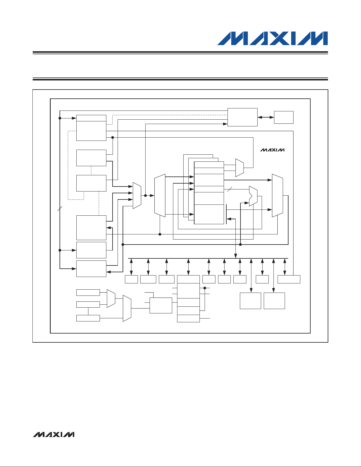
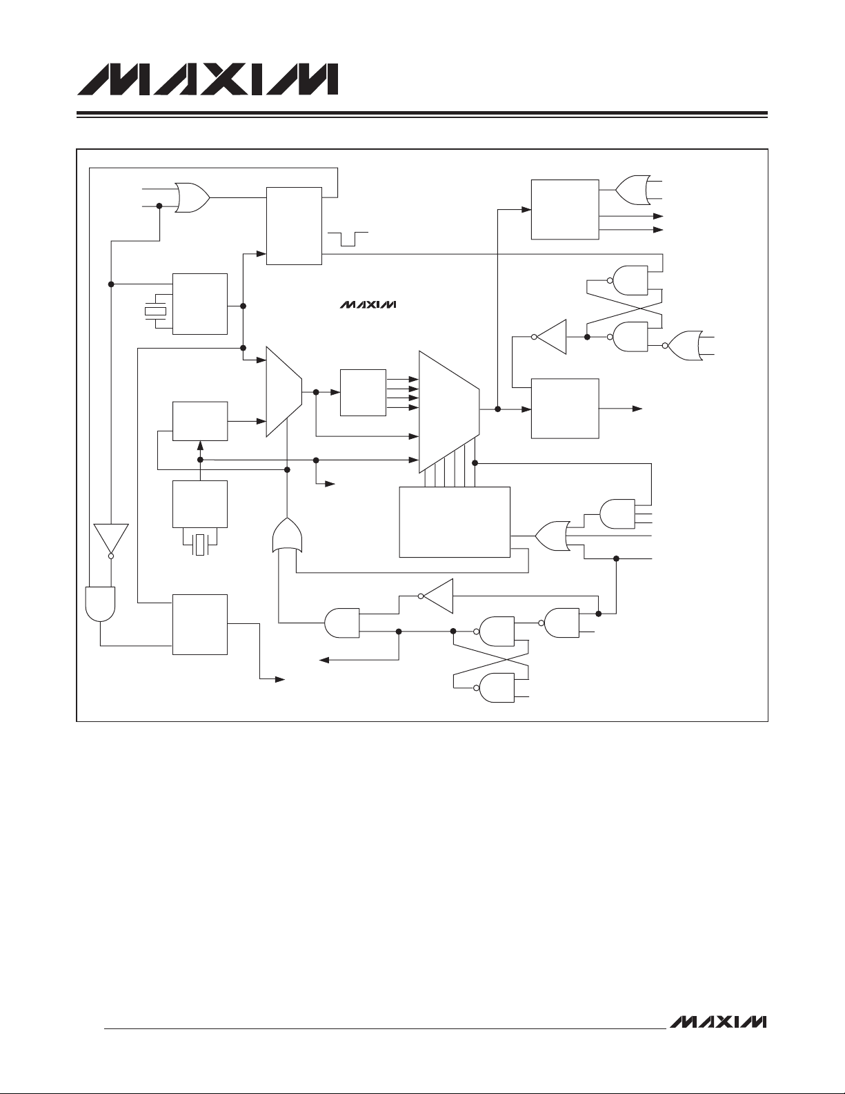
Figure 2-1. MAXQ2010 System and Peripheral Register Map
2-2
HARDWARE
MULTIPLIER
SERIAL,
SPI, I
2
C
LCD
CONTROLLER
TIMERS
ACC
ARRAY,
CONTROL
OTHER
FUNCTIONS
Page 15

MAXQ Family User’s Guide:
MAXQ2010 Supplement
2.4 Memory Organization
As with all MAXQ microcontrollers, the MAXQ2010 contains logically separate program and data memory spaces. All
memory is internal, and physical memory segments (other than the stack and register memories) can be accessed as
either program memory or as data memory, but not both at once.
The MAXQ2010 contains the following physical memory segments.
2.4.1 Register Space
As described in the MAXQ Family User’s Guide, register space on MAXQ microcontrollers consists of 16 register modules, each of which could contain up to 32 registers. Of these possible 16 register modules, only 12 are used on the
MAXQ2010: seven for system registers and five for peripheral registers.
2.4.2 Program Stack
The MAXQ2010 provides a 16 x 16 hardware stack to support subroutine calls and system interrupts. This stack is used
automatically by CALL/RET and PUSH/POP instructions, and can also be accessed directly through the SP register as
described in the MAXQ Family User’s Guide.
When using the in-circuit debugging features, one word of the stack must be reserved to store the return location when
execution branches into the debugging routines in the utility ROM. If in-circuit debug is not used, the entire stack is
available for application use.
2.4.3 Data SRAM
The MAXQ2010 contains up to 1024 words (2KB) of on-chip data SRAM, which can be mapped into either program or
data space. The contents of this SRAM are indeterminate after power-on reset, but are maintained during stop mode
and across non-POR resets.
When using the in-circuit debugging features, the highest 19 bytes of the SRAM must be reserved for saved state storage and working space for the debugging routines in the utility ROM. If in-circuit debug is not used, the entire SRAM
is available for application use.
2.4.4 Program Flash
The MAXQ2010 contains 32KWords (32K x 16) of flash memory, which normally serves as program memory. When
executing from the data SRAM or utility ROM, this memory is mapped to data space (as 32KWords or 64KB) and can
be used for lookup tables and similar functions.
Since program memory is mapped into data space starting at address 8000h, only half the available program memory
can be mapped into data space at one time when operating in byte-access mode. The CDA0 (code data access) bit
is used to control which half of program memory is available in data space as shown in Figure 2-3 and Figure 2-4, and
as described in the MAXQ Family User’s Guide. When operating in word-access mode, the entire 32KWord program
memory can be mapped into data space at once.
Flash memory mapped into data space can be read from directly, like any other type of data memory. However, writing
to flash memory must be done indirectly by calling the in-application functions provided by the utility ROM. See Section
24: Utility ROM for more details.
2.5 Program and Data Memory Mapping
Figures 2-2, 2-3, and 2-4 show the mapping of physical memory segments into the program and data memory space.
The mapping of memory segments into program space is always the same. The mapping of memory segments into
data space varies depending on which memory segment is currently being executed from.
In all cases, whichever memory segment is currently being executed from in program space may not be accessed in
data space.
2-3
Page 16
MAXQ Family User’s Guide:
MAXQ2010 Supplement
DATA SPACE
(BYTE MODE)
4K x 8
UTILITY ROM
2K x 8
DATA SRAM
EXECUTING FROM
PROGRAM
SPACE
1K x 16
DATA SRAM
2K x 16
UTILITY ROM
32K x 16
PROGRAM FLASH
FFFFh
A3FFh
A000h
87FFh
8000h
7FFFh
0000h
Figure 2-2. Memory Map When Executing from Program Flash Memory
DATA SPACE
(WORD MODE)
FFFFh FFFFh
8FFFh
8000h
07FFh
0000h
2K x 16
UTILITY ROM
1K x 16
DATA SRAM
87FFh
8000h
03FFh
0000h
EXECUTING FROM
PROGRAM
SPACE
1K x 16
DATA SRAM
2K x 16
UTILITY ROM
16K x 16
PROGRAM FLASH
(PAGE 1)
16K x 16
PROGRAM FLASH
(PAGE 0)
DATA SPACE
(BYTE MODE, CDA0 = 0)
FFFFh FFFFh
A3FFh
A000h
87FFh
8000h
7FFFh
4000h
3FFFh
0000h
32K x 8
LOWER HALF
(PAGE 0) OF
PROGRAM FLASH
MEMORY
8000h
07FFh
2K x 8
DATA SRAM
0000h
DATA SPACE
(BYTE MODE, CDA0 = 1)
32K x 8
UPPER HALF
(PAGE 1) OF
PROGRAM FLASH
MEMORY
2K x 8
DATA SRAM
FFFFh
8000h
07FFh
0000h
DATA SPACE
(WORD MODE)
FFFFh
32K x 16
PROGRAM FLASH
8000h
03FFh
1K x 16
DATA SRAM
0000h
Figure 2-3. Memory Map When Executing from Utility ROM
2-4
Page 17
MAXQ Family User’s Guide:
MAXQ2010 Supplement
EXECUTING FROM
PROGRAM
SPACE
1K x 16
DATA SRAM
2K x 16
UTILITY ROM
16K x 16
PROGRAM FLASH
(PAGE 1)
16K x 16
PROGRAM FLASH
(PAGE 0)
DATA SPACE
(BYTE MODE, CDA0 = 0)
FFFFh FFFFh
A3FFh
A000h
87FFh
4K x 8
UTILITY ROM
8000h
7FFFh
4000h
3FFFh
0000h
32K x 8
LOWER HALF
(PAGE 0) OF
PROGRAM FLASH
MEMORY
8000h
7FFFh
0000h
DATA SPACE
(BYTE MODE, CDA0 = 1)
4K x 8
UTILITY ROM
32K x 8
UPPER HALF
(PAGE 1) OF
PROGRAM FLASH
MEMORY
FFFFh
8000h
7FFFh
0000h
DATA SPACE
(WORD MODE)
FFFFh
87FFh8FFFh8FFFh
2K x 8
UTILITY ROM
8000h
7FFFh
32K x 16
PROGRAM FLASH
0000h
Figure 2-4. Memory Map When Executing from Data SRAM
2.6 Clock Generation
All functional modules in the MAXQ2010 are synchronized to a single system clock. This system clock can be generated from one of the following clock sources:
• External high-frequency clock
• Internal high-frequency oscillator using external crystal or resonator circuit
• External 32kHz clock
• Internal 32kHz oscillator using external crystal or resonator circuit
• 256x frequency-locked loop (FLL) using 32kHz clock as an input source
The MAXQ2010 does not support an external RC relaxation oscillator circuit, and the FLL takes the place of the ring
oscillator found in some other devices. The 32kHz crystal oscillator could also be used directly by the LCD controller
and the RTC, regardless of the currently selected system clock source.
The following registers and bits are used to control clock generation and selection. For more information, see the register descriptions in this guide and in the MAXQ Family User’s Guide.
2.6.1 External High-Frequency Oscillator Circuit
The high-frequency oscillator operates as described in Section 2.7: Clock Generation of the MAXQ Family User’s
Guide. If used, the external crystal or resonator circuit for this oscillator should be connected between the HFXIN and
HFXOUT pins.
The high-frequency oscillator can be disabled by setting HFXD (PWCN.4) to 1; this is only allowed if the high-frequency
oscillator is not currently being used as the clock source (FLLMD and FLLSL must both equal 1). In this configuration,
an external clock can be used to directly drive HFXIN; refer to the IC data sheet for more details.
2-5
Page 18
MAXQ Family User’s Guide:
MAXQ2010 Supplement
POWER-ON
RESET
STOP
CRYSTAL KLL
HF
CRYSTAL
FLL
ENABLE
32kHz
CRYSTAL
RESET XDOG COUNT
XDOG
STARTUP
TIMER
CLK INPUT
MUX
GLITCH-FREE
XDOG DONE
MAXQ2010
CLOCK
DIVIDER
WAKE-UP
TIMER, LCD
CONTROLLER
DIV 1
DIV 2
SELECTOR
MUX
GLITCH-FREE
DIV 4
DIV 8
32kHz
PMM1
DEFAULT
FLL SELECT
RESET DOG
WATCHDOG
TIMER
ENABLE
CLOCK
GENERATION
RWT
RESET
WATCHDOG RESET
WATCHDOG INTERRUPT
SYSTEM CLOCK
SWB
INTERRUPT/SERIAL PORT
RESET
STOP
STOP
POWER-ON
RESET
INPUT
CRYSTAL
MONITOR
ENABLE
FLLMD
POWER-ON RESET
XDOG DONE
FLLSL
Figure 2-5. MAXQ2010 Clock Sources
2.6.2 External 32kHz Crystal Oscillator Circuit
The 32kHz oscillator operates as described in Section 2.7: Clock Generation of the MAXQ Family User’s Guide. It cannot be used directly as a system clock source, but instead works as an input to the FLL. It can also be used directly by
the LCD controller and RTC modules, regardless of the current system clock source selection. This clock can be generated by an internal 32kHz crystal oscillator, using an external crystal connected between the 32KIN and 32KOUT pins.
Setting X32D (PWCN.2) to 1 disables the 32kHz clock source completely. This should only be done when all the following conditions are true:
• Either the high-frequency oscillator is being used as the system clock source, or if the FLL is being used as the
system clock source, it is already enabled and locked.
• The 32kHz clock is not being used to drive either the RTC or the LCD controller.
If X32D = 0, the control bit X32KBYP (PWCN.5) can be used to switch between the internal oscillator and external
32kHz clock modes of operation.
2-6
Page 19

MAXQ Family User’s Guide:
MAXQ2010 Supplement
Table 2-1. System Clock Generation and Control Registers
REGISTER ADDRESS BIT(S) FUNCTION
000: System clock = high-frequency clock divided by 1.
001: System clock = high-frequency clock divided by 2.
010: System clock = high-frequency clock divided by 4.
011: System clock = high-frequency clock divided by 8.
1xx: System clock = high-frequency clock/256.
CKCN M8[0Eh]
[2:0]—PMME,
CD[1:0]
CKCN M8[0Eh] 5—FLLMD
CKCN M8[0Eh] 6—FLLSL
PWCN M0[0Fh] 0—FLLEN
PWCN M0[0Fh] 1—FLOCK
PWCN M0[0Fh] 2—X32D
PWCN M0[0Fh] 3—X32KRDY
PWCN M0[0Fh] 4—HFXD
PWCN M0[0Fh] 5—X32KBYP
PWCN M0[0Fh] [9:8]—X32KMD
0: System clock is being provided by an external source.
1: System clock is being provided by the FLL.
0: Selects an external source for system clock generation.
1: Selects the FLL for system clock generation.
0: Disables the FLL (unless it is providing the system clock).
1: Enables the FLL and locks it to the 32kHz input.
0: Indicates the FLL is disabled or in the process of locking.
1: Indicates the FLL is locked to the 32kHz input.
0: 32kHz clock or oscillator operates normally (default).
1: Disables the 32kHz source completely (except in stop).
0: Indicates the 32kHz oscillator is still warming up.
1: Indicates the 32kHz oscillator is ready for use.
0: High-frequency oscillator operates normally (default).
1: Disables the high-frequency oscillator, allowing an external clock to be
provided at HFXIN.
0: 32kHz clock is provided by internal oscillator (default).
1: Disables the 32kHz oscillator, allowing an external clock to be provided at
32KIN.
00: 32kHz oscillator operates in noise immune mode.
01: 32kHz oscillator operates in quiet mode.
10: 32kHz oscillator operates in noise immune mode normally and in quiet mode
during stop mode. (Note: This setting should not be used on devices of rev
B3 or earlier; refer to the device errata for more details.)
11: 32kHz oscillator operates in quiet mode normally and in noise immune mode
during stop mode.
2.6.3 Frequency-Locked Loop (FLL)
The MAXQ2010 contains an FLL circuit that provides an optional, low-cost method of generating a high-frequency
system clock. The FLL uses the 32kHz clock as an input, multiplying its frequency by 256 to generate a clock output of
approximately 8.4MHz (refer to the IC data sheet for details). This clock output can be used as a system clock source.
On power-on reset, the FLL is automatically enabled as the system clock source while the high-frequency oscillator
warms up. Once the warmup count for the high-frequency oscillator has completed, the clock source switches to the
high-frequency oscillator automatically. If no external crystal or resonator circuit is provided at HFXIN, the switchover
never occurs, and the clock runs from the FLL indefinitely.
To select the FLL as the system clock source permanently, the FLLSL bit (CKCN.6) must be set to 1. Setting this bit
immediately switches over the system clock source to the FLL. The FLLMD (CKCN.5) bit indicates the current system
clock source. If the FLL is currently providing the system clock, FLLMD = 1; otherwise, FLLMD = 0.
Since the FLLSL bit is cleared by power-on reset only, if this bit is set before entering stop mode, the FLL is still used
as the system clock source when stop mode is exited. In this case, a four-cycle warmup delay is required when exiting
stop mode before execution resumes using the FLL as the system clock source.
2-7
Page 20

MAXQ Family User’s Guide:
MAXQ2010 Supplement
When the system clock source is switched back from the FLL to the high-frequency oscillator by clearing FLLSL to
zero, the FLL is still used as the system clock source until the warmup period has completed for the high-frequency
oscillator. This is reflected by the value of the FLLMD bit, which remains at 1 until the warmup for the high-frequency
oscillator has completed and the clock switches over, at which point FLLMD switches to 0.
2.7 Interrupts
In general, interrupt handling on the MAXQ2010 operates as described in the MAXQ Family User’s Guide. All interrupt
sources have the same priority, and all interrupts cause program execution to branch to the location specified by the
Interrupt Vector (IV) register, which defaults to 0000h.
Table 2-2 lists all possible interrupt sources for the MAXQ2010, along with their corresponding module interrupt enable
bits, local interrupt enable bits, and interrupt flags.
• Each module interrupt enable bit, when cleared to 0, blocks interrupts originating in that module from being acknowledged. When the module interrupt enable bit is set to 1, interrupts from that module are acknowledged (unless all
interrupts have been disabled globally).
• Each local interrupt enable bit, when cleared to 0, disables the corresponding interrupt. When the local interrupt-
enable bit is set to 1, the interrupt is triggered whenever its interrupt flag is set to 1 by hardware or by software.
• Each interrupt flag bit, when set to 1, causes its corresponding interrupt to trigger. Interrupt flag bits are typically set
by hardware and must be cleared by software (generally in the interrupt handler routine).
Note that for an interrupt to fire, the following five conditions must exist:
• Interrupts must be enabled globally by setting IGE (IC.0) to 1.
• The module interrupt enable bit for the interrupt source’s module must be set to 1.
• The local interrupt enable bit for the specific interrupt source must be set to 1.
• The interrupt flag for the interrupt source must be set to 1. Typically, this is done by hardware when the condition
that requires interrupt service occurs.
• The interrupt-in-service (INS) bit must be cleared to 0. This bit is set automatically upon vectoring to the interrupt
handler (IV) address and cleared automatically upon exit (RETI/POPI), so the only reason to clear this bit manually
(inside the interrupt handler routine) is to allow nested interrupt handling.
Table 2-2. Interrupt Sources and Control Bits
INTERRUPT MODULE ENABLE BIT LOCAL ENABLE BIT INTERRUPT FLAG
Watchdog Interrupt IMS (IMR.7) EWDI (WDCN.6) WDIF (WDCN.3)
External Interrupt 0 (P0.0) IM0 (IMR.0) EX0 (EIE0.0) IE0 (EIF0.0)
External Interrupt 1 (P0.1) IM0 (IMR.0) EX1 (EIE0.1) IE1 (EIF0.1)
External Interrupt 2 (P0.2) IM0 (IMR.0) EX2 (EIE0.2) IE2 (EIF0.2)
External Interrupt 3 (P0.3) IM0 (IMR.0) EX3 (EIE0.3) IE3 (EIF0.3)
External Interrupt 4 (P0.4) IM0 (IMR.0) EX4 (EIE0.4) IE4 (EIF0.4)
External Interrupt 5 (P0.5) IM0 (IMR.0) EX5 (EIE0.5) IE5 (EIF0.5)
External Interrupt 6 (P0.6) IM0 (IMR.0) EX6 (EIE0.6) IE6 (EIF0.6)
External Interrupt 7 (P0.7) IM0 (IMR.0) EX7 (EIE0.7) IE7 (EIF0.7)
RTC Time-of-Day Alarm IM0 (IMR.0) ADE (RCNT.1) ALDF (RCNT.6)
RTC Subsecond Alarm IM0 (IMR.0) ASE (RCNT.2) ALSF (RCNT.7)
External Interrupt 8 (P5.0) IM1 (IMR.1) EX8 (EIE1.0) IE8 (EIF1.0)
External Interrupt 9 (P5.1) IM1 (IMR.1) EX9 (EIE1.1) IE9 (EIF1.1)
External Interrupt 10 (P5.2) IM1 (IMR.1) EX10 (EIE1.2) IE10 (EIF1.2)
External Interrupt 11 (P5.3) IM1 (IMR.1) EX11 (EIE1.3) IE11 (EIF1.3)
External Interrupt 12 (P5.4) IM1 (IMR.1) EX12 (EIE1.4) IE12 (EIF1.4)
2-8
Page 21

MAXQ Family User’s Guide:
MAXQ2010 Supplement
Table 2-2. Interrupt Sources and Control Bits (continued)
INTERRUPT MODULE ENABLE BIT LOCAL ENABLE BIT INTERRUPT FLAG
External Interrupt 13 (P5.5) IM1 (IMR.1) EX13 (EIE1.5) IE13 (EIF1.5)
External Interrupt 14 (P5.6) IM1 (IMR.1) EX14 (EIE1.6) IE14 (EIF1.6)
External Interrupt 15 (P6.0) IM1 (IMR.1) EX15 (EIE2.0) IE15 (EIF2.0)
External Interrupt 16 (P6.1) IM1 (IMR.1) EX16 (EIE2.1) IE16 (EIF2.1)
External Interrupt 17 (P6.2) IM1 (IMR.1) EX17 (EIE2.2) IE17 (EIF2.2)
External Interrupt 18 (P6.3) IM1 (IMR.1) EX18 (EIE2.3) IE18 (EIF2.3)
External Interrupt 19 (P6.4) IM1 (IMR.1) EX19 (EIE2.4) IE19 (EIF2.4)
External Interrupt 20 (P6.5) IM1 (IMR.1) EX20 (EIE2.5) IE20 (EIF2.5)
External Interrupt 21 (P6.6) IM1 (IMR.1) EX21 (EIE2.6) IE21 (EIF2.6)
External Interrupt 22 (P6.7) IM1 (IMR.1) EX22 (EIE2.7) IE22 (EIF2.7)
Supply Voltage Monitor Interrupt IM1 (IMR.1) SVMIE (SVM.2) SVMI (SVM.3)
SPI Mode Fault Interrupt IM1 (IMR.1) ESPII (SPICF.7) MODF (SPICN.3)
SPI Write Collision Interrupt IM1 (IMR.1) ESPII (SPICF.7) WCOL (SPICN.4)
SPI Receive Overrun Interrupt IM1 (IMR.1) ESPII (SPICF.7) ROVR (SPICN.5)
SPI Transfer Complete Interrupt IM1 (IMR.1) ESPII (SPICF.7) SPIC (SPICN.6)
I2C START Condition Interrupt IM3 (IMR.3) I2CSRI (I2CST.0) I2CSRIE (I2CIE.0)
I2C Transmit Complete Interrupt IM3 (IMR.3) I2CTXI (I2CST.1) I2CTXIE (I2CIE.1)
I2C Receive Ready Interrupt IM3 (IMR.3) I2CRXI (I2CST.2) I2CRXIE (I2CIE.2)
I2C Clock Stretch Interrupt IM3 (IMR.3) I2CSTRI (I2CST.3) I2CSTRIE (I2CIE.3)
I2C Timeout Interrupt IM3 (IMR.3) I2CTOI (I2CST.4) I2CTOIE (I2CIE.4)
I2C Slave Address Match Interrupt IM3 (IMR.3) I2CAMI (I2CST.5) I2CAMIE (I2CIE.5)
I2C Arbitration Loss Interrupt IM3 (IMR.3) I2CALI (I2CST.6) I2CALIE (I2CIE.6)
I2C NACK Interrupt IM3 (IMR.3) I2CNACKI (I2CST.7) I2CNACKIE (I2CIE.7)
I2C General Call Address Interrupt IM3 (IMR.3) I2CGCI (I2CST.8) I2CGCIE (I2CIE.8)
I2C Receiver Overrun Interrupt IM3 (IMR.3) I2CROI (I2CST.9) I2CROIE (I2CIE.9)
I2C STOP Condition Interrupt IM3 (IMR.3) I2CSPI (I2CST.11) I2CSPIE (I2CIE.11)
Serial Port 0 Receive IM3 (IMR.3) ESI (SMD0.2) RI (SCON0.0)
Serial Port 0 Transmit IM3 (IMR.3) ESI (SMD0.2) TI (SCON0.1)
Serial Port 1 Receive IM3 (IMR.3) ESI (SMD1.2) RI (SCON1.0)
Serial Port 1 Transmit IM3 (IMR.3) ESI (SMD1.2) TI (SCON1.1)
ADC Data Available Interrupt IM4 (IMR.4) ADDAIE (ADCN.5) ADDAI (ADST.5)
Type B Timer 0—External Trigger IM4 (IMR.4) EXFB (TB0CN.6) ETB (TB0CN.1)
Type B Timer 0—Overflow IM4 (IMR.4) TFB (TB0CN.7) ETB (TB0CN.1)
Type B Timer 1—External Trigger IM4 (IMR.4) EXFB (TB1CN.6) ETB (TB1CN.1)
Type B Timer 1—Overflow IM4 (IMR.4) TFB (TB1CN.7) ETB (TB1CN.1)
Type B Timer 2—External Trigger IM4 (IMR.4) EXFB (TB2CN.6) ETB (TB2CN.1)
Type B Timer 2—Overflow IM4 (IMR.4) TFB (TB2CN.7) ETB (TB2CN.1)
2.8 Reset Conditions
There are four possible reset sources for the MAXQ2010. While in the reset state, the enabled system clock oscillator
continues running, but no code execution occurs. Once the reset condition has been removed or has completed, code
execution resumes at address 8000h for all reset types.
2-9
Page 22
MAXQ Family User’s Guide:
MAXQ2010 Supplement
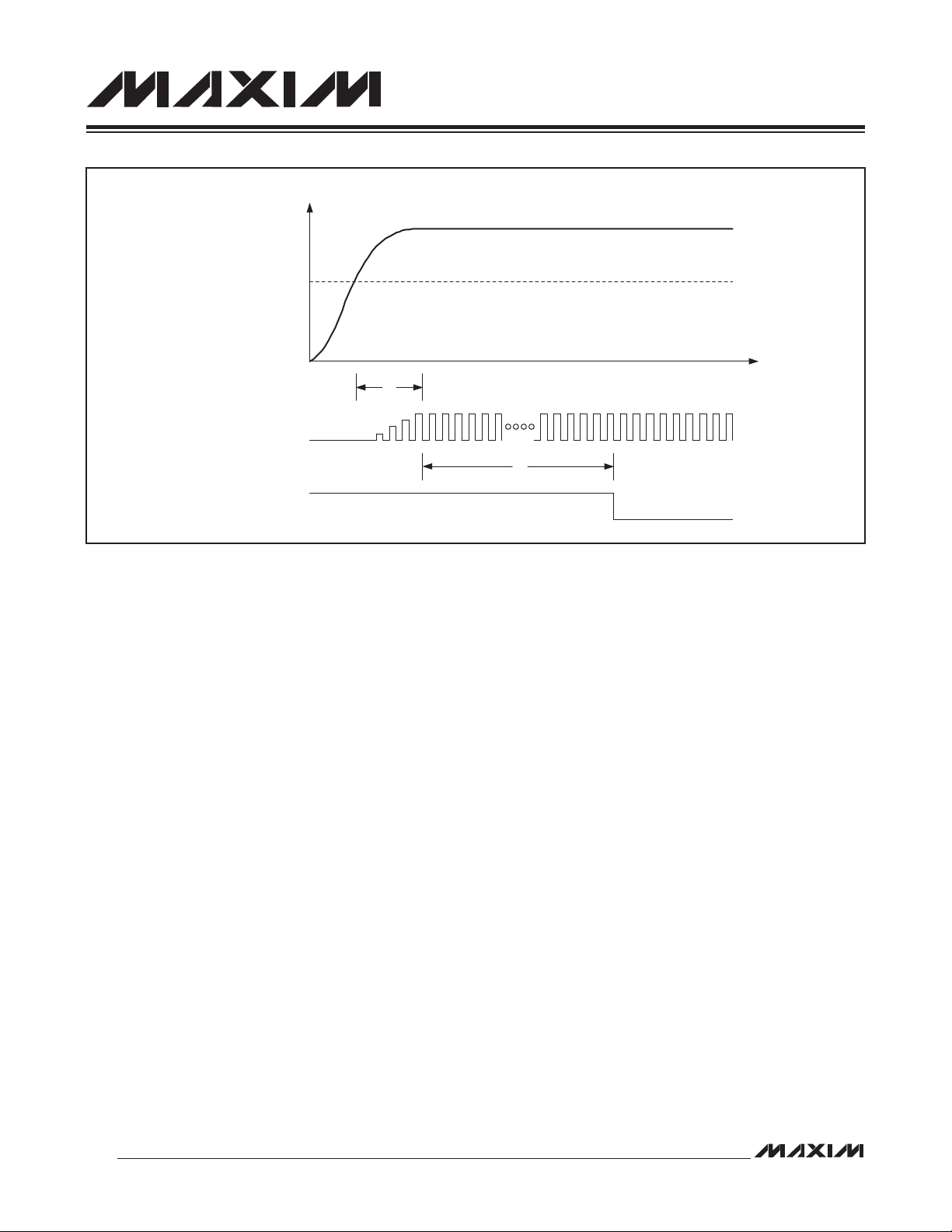
SUPPLY AT V
FREQUENCY-LOCKED LOOP
INTERNAL RESET
Figure 2-6. Power-On Reset Timing
DD
V
RST
T1
(T1 = STARTUP TIME FOR FLL)
T2
(T2 = 65,536 FLL CYCLES, OR 7.84ms AT 8.4MHz)
2.8.1 Power-On Reset
When power is first applied to the MAXQ2010, or when the supply voltage at VDD drops below the V
processor is held in a power-on reset state. See Figure 2-6. For the MAXQ2010 to exit power-on reset, the following
two conditions must apply:
• The supply voltage at VDD is above the power-on reset level V
RST.
• The FLL has completed 65,536 cycles (delay for power supply to stabilize).
level, the
RST
2.8.2 Watchdog Timer Reset
The watchdog timer on the MAXQ2010 functions as described in the MAXQ Family User’s Guide.
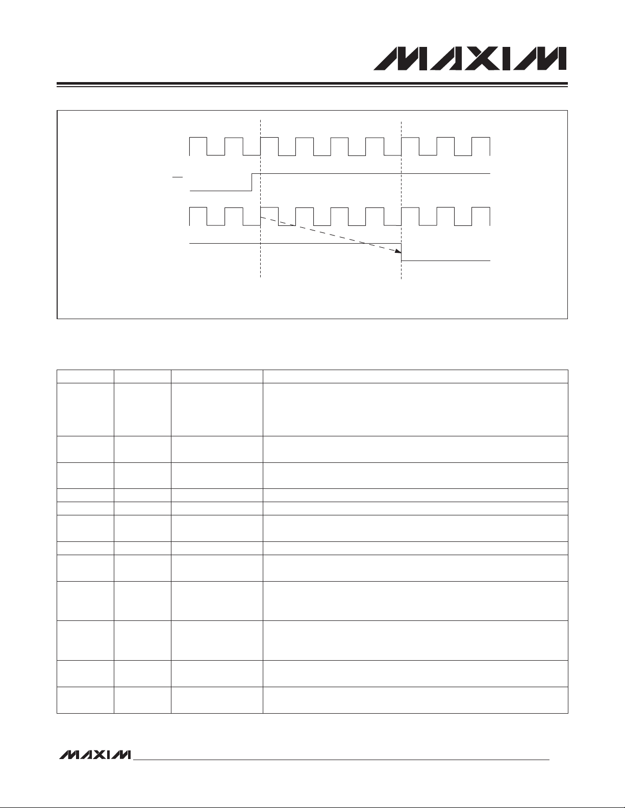
2.8.3 External Reset
External reset through the RST input is a synchronous reset source. After the external reset low has been removed and
sampled, execution resumes following a delay of four clock cycles, as shown in Figure 2-7.
2.9 Power-Management Features
The MAXQ2010 provides the following features to assist in power management:
• Divide-by-256 (PMM) mode to reduce current consumption.
• Switchback mode to exit PMM mode automatically when rapid processing is required.
• Ultra-low-power stop mode.
• Selective regulator and brownout detection disable during stop mode.
• Selectable noise immune mode or quiet mode for 32kHz oscillator operation.
Table 2-3 shows the system registers and bits used to control power-management features. For more information, see
the register descriptions in this document and in the MAXQ Family User’s Guide.
2-10
Page 23
MAXQ Family User’s Guide:
MAXQ2010 Supplement
CLOCK
RST
RESET SAMPLING
INTERNAL RESET
Figure 2-7. External Reset Timing
FIRST
INSTRUCTION
FETCH
Table 2-3. System Power-Management Registers
REGISTER ADDRESS BIT FUNCTION
00: System clock = high-frequency clock divided by 1.
CKCN M8[0Eh] [1:0]—CD[1:0]
CKCN M8[0Eh] 2—PMME
CKCN M8[0Eh] 3—SWB
CKCN M8[0Eh] 4—STOP When set to 1, causes the processor to enter stop mode.
PWCN M0[0Fh] 0—FLLEN When set to 1, enables the FLL and causes it to lock to the 32kHz input.
PWCN M0[0Fh] 1—FLOCK
PWCN M0[0Fh] 2—X32D When set to 1, disables the 32kHz clock source.
PWCN M0[0Fh] 3—X32KRDY
PWCN M0[0Fh] 4—HFXD
PWCN M0[0Fh] 5—X32KBYP
PWCN M0[0Fh] 6—REGEN
PWCN M0[0Fh] 7—BOD
01: System clock = high-frequency clock divided by 2.
10: System clock = high-frequency clock divided by 4.
11: System clock = high-frequency clock divided by 8.
0: System clock is determined by the settings of CD[1:0].
1: System clock = high-frequency clock divided by 256.
When set to 1, enables automatic switchback from PMM (divide-by-256
mode) to normal clock-divide mode under certain conditions.
0: FLL is disabled or warming up.
1: FLL is enabled and locked to the 32kHz input.
Read-only status bit; when 1, indicates that the 32kHz clock is ready for
use.
0: Enables the high-frequency oscillator.
1: Disables the high-frequency oscillator, allowing an external clock to be
provided at HFXIN.
0: Enables the internal 32kHz oscillator.
1: Disables the internal 32kHz oscillator, allowing an external clock to be
provided at 32KIN.
0: Internal regulator is shut down during stop mode.
1: Internal regulator remains powered on during stop mode.
0: Brownout detection remains enabled during stop mode.
1: Brownout detection is enabled during stop mode.
2-11
Page 24

MAXQ Family User’s Guide:
MAXQ2010 Supplement
Table 2-3. System Power-Management Registers (continued)
REGISTER ADDRESS BIT FUNCTION
Selects operating mode of the 32kHz oscillator as follows.
00: Always operate in noise immune mode.
01: Always operate in quiet mode.
10: Operate in noise immune mode normally and in quiet mode during stop.
PWCN M0[0Fh] [9:8]—X32KMD[1:0]
PWCN M0[0Fh] 15—FREQMD
2.9.1 Divide-by-256 Mode (PMM)
In this power-management mode, all operations continue as normal, but at a reduced clock rate (the high-frequency
clock divided by 256). This power-management mode affects module clock rates as follows:
• Program execution occurs at the high-frequency clock rate divided by 256.
• The RTC module continues to operate using the 32kHz clock.
• The LCD module continues to operate using its originally selected clock, which is either the high-frequency clock
divided by 512 or the 32kHz clock, as selected by the LCCS bit (LCRA.6).
• All other functional modules (timers, USARTs, SPI) operate at the high-frequency clock rate divided by 256.
This power-management mode is entered by setting the PMME bit (CKCN.2) to 1. When PMM mode is exited (either
by clearing the PMME bit or as a result of a switchback trigger), system operation reverts to divide-by-1 mode.
Wait for 32kHz oscillator warmup upon stop mode exit. (Note: This setting
should not be used on devices of rev B3 or earlier; refer to the device
errata for more details.)
11: Operate in noise immune mode normally and in quiet mode during stop.
Skip 32kHz oscillator warmup upon stop mode exit.
This bit is used to adjust the operating mode of the MAXQ2010 to provide
optimal current consumption based on operating frequency. Typically,
when running at a frequency of 3MHz or higher, this bit should be set to
0 to optimize current consumption. When running at a frequency under
3MHz, this bit should typically be set to 1. Refer to the “VDD Supply Current
vs. Clock Frequency” graph in the IC data sheet for more details.
2.9.2 Switchback Mode
As described in the MAXQ Family User’s Guide, switchback mode is used to provide an automatic exit from powermanagement mode when a higher clock rate is required to respond to I/O, such as USART activity, SPI activity, or an
external interrupt.
Switchback mode is enabled when the SWB (CKCN.3) bit is set to 1 and the PMME (CKCN.2) bit is set to 1 (the system
is in the PMM mode). If switchback is enabled, the PMME bit is cleared (causing the system to exit power-management
mode) when any of the following conditions occur:
• An external interrupt condition occurs on an external interrupt pin and the corresponding external interrupt is enabled.
• An active-low transition occurs on the RXD0 or RXD1 pin, and the corresponding USART is enabled to receive data.
• The SBUF0 or SBUF1 register is written to transmit a byte over the corresponding USART.
• The SPIB register is written to transmit a byte with the SPI interface enabled in master mode.
• The SSEL signal is asserted low with the SPI interface enabled in slave mode.
• A START condition occurs on the I2C bus and the I2C start interrupt is triggered.
• The supply voltage drops below the supply voltage monitor (SVM) threshold, and the SVM interrupt is triggered.
• A time-of-day alarm is generated by the RTC module.
• A subsecond alarm is generated by the RTC module.
2-12
Page 25

MAXQ Family User’s Guide:
MAXQ2010 Supplement
• An ADC conversion is initiated by setting ADCONV to 1.
• Active debug mode is entered either by a breakpoint match or direct issuance of the debug command from back-
ground mode.
As described in the MAXQ Family User’s Guide, if any of these conditions is true (a switchback source is active) and
the SWB bit has been set, the PMME bit cannot be set to enter power-management mode.
2.9.3 Stop Mode
Stop mode disables all circuits within the MAXQ2010 except for the 32kHz crystal amplifier and any circuitry that is
clocked directly by the 32kHz clock. All other on-chip clocks, timers, serial ports, and other peripherals are stopped,
and no code execution occurs. Once in stop mode, the MAXQ2010 is in a near-static state, with power consumption
determined largely by leakage currents.
The RTC always continues to run during stop mode if it was enabled upon stop mode entry. The LCD controller continues to run during stop mode if the following conditions are true:
• The 32kHz clock is selected as the LCD controller clock source (LCCS = 0).
• The LCD controller is in normal operation mode (OPM = 1).
• The LCD controller is enabled to operate during stop mode (SMO = 1).
Stop mode is invoked by setting the STOP bit to 1. The MAXQ2010 enters stop mode immediately when the STOP bit
is set. Entering stop mode does not affect the setting of the clock control bits; this allows the system to return to its
original operating frequency following stop mode removal.
The processor exits stop mode if any of the following conditions occur. In order to exit stop mode by means of an interrupt, the interrupt must be enabled globally, by module, and locally prior to entering stop mode.
• External reset (from the RST pin)
• Power-on/brownout reset
• External interrupt
• RTC time-of-day or subsecond alarm
• I2C start interrupt
• Supply voltage monitor interrupt (SVMSTOP must be set to 1)
Note that exiting stop mode through external reset or power-on reset causes the processor to undergo a normal reset
cycle, as opposed to resuming execution at the point at which it entered stop mode. Exiting stop mode by means of
an interrupt or RTC alarm causes the processor to vector to the interrupt handler routine at IV. Following the completion
of the interrupt handler, execution resumes at the instruction following the one that caused the entry into stop mode.
When the processor exits stop mode, program execution resumes after approximately four FLL oscillator cycles (refer
to the IC data sheet for timing details). The clock source following stop mode exit is selected as follows:
• If FLLSL = 1, the processor continues running from the FLL indefinitely.
• If FLLSL = 0, the processor continues running from the FLL until the high-frequency clock source completes its
65,536-cycle warmup count, at which point it switches over to the high-frequency clock automatically.
Note: The MAXQ2010 powers down parts of the memory interface during stop mode to conserve power. Because
of this, application code must always “re-prime” the active data pointer (DP[0], DP[1], or BP[OFFS]) following
any exit from stop mode before using that data pointer to read from memory. This can be accomplished by:
• Writing a new address (or rewriting the existing address) to the active data pointer.
• Writing to the DPC register to select a new data pointer (or reselect the active data pointer).
2-13
Page 26

MAXQ Family User’s Guide:
MAXQ2010 Supplement
ADDENDUM TO SECTION 3: PROGRAMMING
Refer to Section 3: Programming of the MAXQ Family User’s Guide for examples of general program operations involv-
ing the MAXQ core. The MAXQ2010 contains the MAXQ20 (16-bit accumulator version) of the MAXQ core.
3-1
Page 27
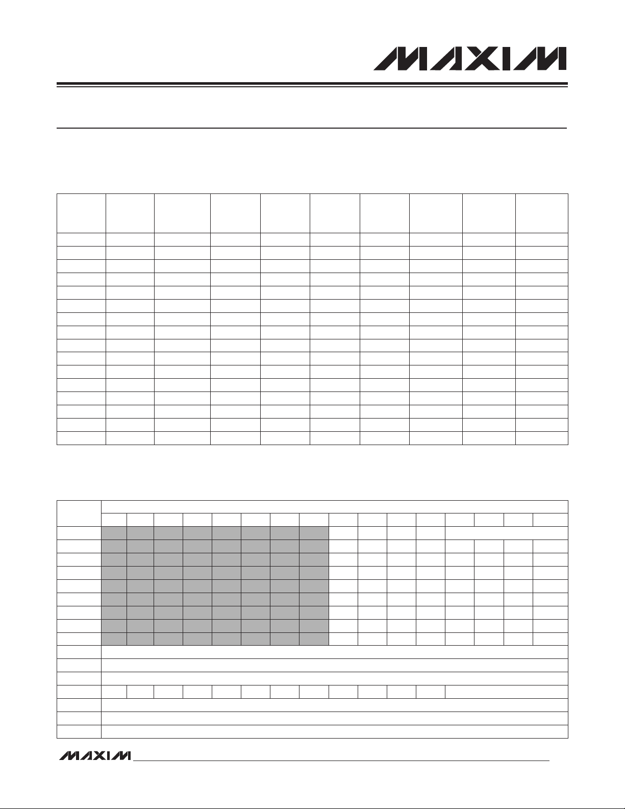
MAXQ Family User’s Guide:
MAXQ2010 Supplement
ADDENDUM TO SECTION 4: SYSTEM REGISTER DESCRIPTIONS
Refer to Section 4: System Register Descriptions of the MAXQ Family User’s Guide for functional descriptions of the
registers and bits in Table 4-1.
Table 4-1. System Register Map
CYCLES
TO
READ
1 1 00h AP
1 1 01h APC
1 1 02h —
1 1 03h —
1 1 04h PSF
1 1 05h IC
1 1 06h IMR
1 1 07h —
1 2 08h SC
1 2 09h —
1 2 0Ah —
1 2 0Bh IIR
1 2 0Ch —
1 2 0Dh —
1 2 0Eh CKCN
1 2 0Fh WDCN
Note: Register names that appear in italics indicate read-only registers. Register names that appear in bold indicate 16-bit registers. All other registers are 8 bits in width.
CYCLES
TO
WRITE
REGISTER
INDEX
M8 M9 M11 M12 M13 M14 M15
A[0] PFX[0] IP
A[1] PFX[1]
A[2] PFX[2]
A[3] PFX[3]
A[4] PFX[4]
A[5] PFX[5]
A[6] PFX[6]
A[7] PFX[7]
A[8]
A[9]
A[10]
A[11]
A[12]
A[13]
A[14]
A[15]
— — —
— — — GRH —
— — —
— — —
— — — — —
— — — — —
— — — — —
— — — — —
—
—
— — OFFS
— —
— —
—
—
— — —
SP
IV
LC[0]
LC[1] BP DP[1]
— —
— —
DPC
GR
GRL —
GRS
GRXL
BP[OFFS]
DP[0]
—
—
—
—
—
Table 4-2. System Register Bit Functions
REG
AP — — — — AP (4 bits)
APC CLR IDS — — — MOD2 MOD1 MOD0
PSF Z S — GPF1 GPF0 OV C E
IC — — — — — — INS IGE
IMR IMS — — IM4 IM3 IM2 IM1 IM0
SC TAP — — CDA0 — — PWL —
IIR IIS — — II4 II3 II2 II1 II0
CKCN — FLLSL FLLMD STOP SWB PMME CD1 CD0
WDCN POR EWDI WD1 WD0 WDIF WTRF EWT RWT
A[0:15] A[0:15] (16 bits)
PFX PFX (16 bits)
IP IP (16 bits)
SP — — — — — — — — — — — — SP (4 bits)
IV IV (16 bits)
LC[0] LC[0] (16 bits)
LC[1] LC[1] (16 bits)
15 14 13 12 11 10 9 8 7 6 5 4 3 2 1 0
BIT
4-1
Page 28
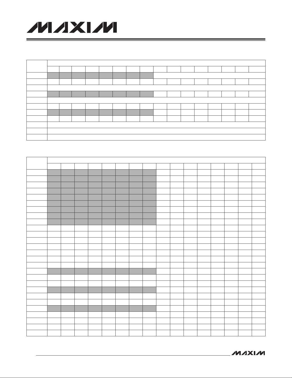
MAXQ Family User’s Guide:
MAXQ2010 Supplement
Table 4-2. System Register Bit Functions (continued)
REG
OFFS OFFS (8 bits)
DPC — — — — — — — — — — — WBS2 WBS1 WBS0 SDPS1 SDPS0
GR GR (16 bits)
GRL GR.7 GR.6 GR.5 GR.4 GR.3 GR.2 GR.1 GR.0
BP BP (16 bits)
GRS GR.7 GR.6 GR.5 GR.4 GR.3 GR.2 GR.1 GR.0 GR.15 GR.14 GR.13 GR.12 GR.11 GR.10 GR.9 GR.8
GRH GR.15 GR.14 GR.13 GR.12 GR.11 GR.10 GR.9 GR.8
GRXL GR.7 GR.7 GR.7 GR.7 GR.7 GR.7 GR.7 GR.7 GR.7 GR.6 GR.5 GR.4 GR.3 GR.2 GR.1 GR.0
BP[OFFS] BP[OFFS] (16 bits)
DP[0] DP[0] (16 bits)
DP[1] DP[1] (16 bits)
15 14 13 12 11 10 9 8 7 6 5 4 3 2 1 0
Table 4-3. System Register Reset Values
REG
AP 0 0 0 0 0 0 0 0
APC 0 0 0 0 0 0 0 0
PSF 1 0 0 0 0 0 0 0
IC 0 0 0 0 0 0 0 0
IMR 0 0 0 0 0 0 0 0
SC 1 0 0 0 0 0 s 0
IIR 0 0 0 0 0 0 0 0
CKCN 1 s s 0 0 0 0 0
WDCN s s 0 0 0 s s 0
A[0:15] 0 0 0 0 0 0 0 0 0 0 0 0 0 0 0 0
PFX 0 0 0 0 0 0 0 0 0 0 0 0 0 0 0 0
IP 1 0 0 0 0 0 0 0 0 0 0 0 0 0 0 0
SP 0 0 0 0 0 0 0 0 0 0 0 0 1 1 1 1
IV 0 0 0 0 0 0 0 0 0 0 0 0 0 0 0 0
LC[0] 0 0 0 0 0 0 0 0 0 0 0 0 0 0 0 0
LC[1] 0 0 0 0 0 0 0 0 0 0 0 0 0 0 0 0
OFFS 0 0 0 0 0 0 0 0
DPC 0 0 0 0 0 0 0 0 0 0 0 1 1 1 0 0
GR 0 0 0 0 0 0 0 0 0 0 0 0 0 0 0 0
GRL 0 0 0 0 0 0 0 0
BP 0 0 0 0 0 0 0 0 0 0 0 0 0 0 0 0
GRS 0 0 0 0 0 0 0 0 0 0 0 0 0 0 0 0
GRH 0 0 0 0 0 0 0 0
GRXL 0 0 0 0 0 0 0 0 0 0 0 0 0 0 0 0
BP[OFFS] 0 0 0 0 0 0 0 0 0 0 0 0 0 0 0 0
DP[0] 0 0 0 0 0 0 0 0 0 0 0 0 0 0 0 0
DP[1] 0 0 0 0 0 0 0 0 0 0 0 0 0 0 0 0
Note: Bits marked as “s” have special behavior upon reset; see the register descriptions for details.
15 14 13 12 11 10 9 8 7 6 5 4 3 2 1 0
BIT
BIT
4-2
Page 29
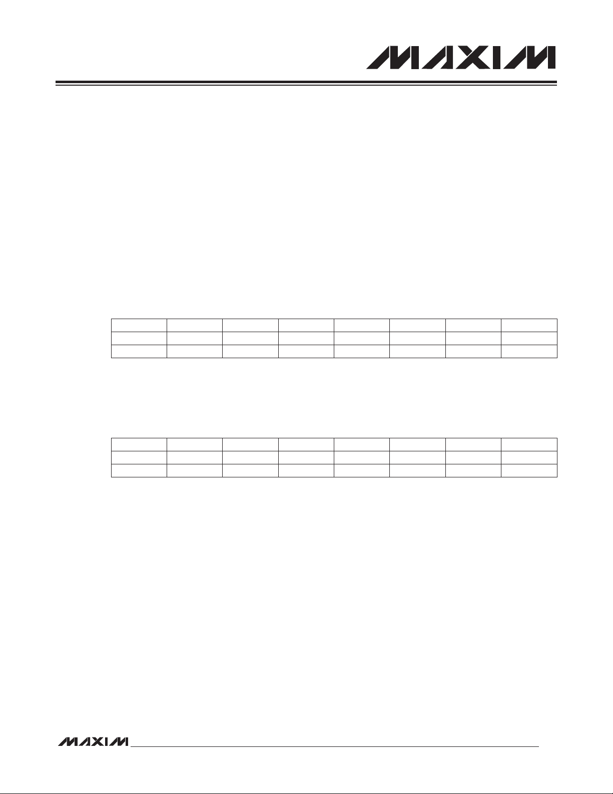
MAXQ Family User’s Guide:
MAXQ2010 Supplement
4.1 System Register Descriptions
This section details the functionality of any system register contained in the MAXQ2010 that operates differently from its
description in the MAXQ Family User’s Guide. Addresses for all system and peripheral registers are given as “Mx[yy],”
where x is the module number (from 0 to 15 decimal) and yy is the register index (from 00h to 1Fh hexadecimal). Fields
in the bit definition tables are defined as follows:
• Name: Symbolic names of bits or bit fields in this register.
• Reset: The value of each bit in this register following a standard reset. If this field reads “unchanged,” the given bit
is unaffected by standard reset. If this field reads “s,” the given bit does not have a fixed 0 or 1 reset value because
its value is determined by another internal state or external condition.
• POR: If present this field defines the value of each bit in this register following a power-on reset (as opposed to a
standard reset). Some bits are unaffected by standard resets and are set/cleared by POR only.
• Access: Bits can be read-only (r) or read/write (rw). Any special restrictions or conditions that could apply when
reading or writing this bit are detailed in the bit description.
4.1.1 Processor Status Flags Register (PSF, M8[04h])
Bit #
Name Z S — GPF1 GPF0 OV C E
Reset 1 0 0 0 0 0 0 0
Access r r r rw rw rw rw rw
7 6 5 4 3 2 1 0
This register operates as described in the MAXQ Family User’s Guide, with the exception that the overflow bit (OV)
can be written by software.
4.1.2 Interrupt Mask Register (IMR, M8[06h])
Bit #
Name IMS — — IM4 IM3 IM2 IM1 IM0
Reset 0 0 0 0 0 0 0 0
Access rw r r rw rw rw rw rw
The first five bits in this register are interrupt mask bits for modules 0 to 4, one bit per module. The eighth bit, IMS,
serves as a mask for any system module interrupt sources. Setting a mask bit allows the enabled interrupt sources for
the associated module or system (with IMS) to generate interrupt requests. Clearing the mask bit effectively disables
all interrupt sources associated with that module or, in the case of IMS, all system interrupt sources. The IMR register
is intended to facilitate user-definable interrupt prioritization.
Bit 7: System Module Interrupt Mask (IMS)
Bits 5:6: Reserved
Bit 4: Module 4 Interrupt Mask (IM4)
Bit 3: Module 3 Interrupt Mask (IM3)
Bit 2: Module 2 Interrupt Mask (IM2)
Bit 1: Module 1 Interrupt Mask (IM1)
Bit 0: Module 0 Interrupt Mask (IM0)
7 6 5 4 3 2 1 0
4-3
Page 30
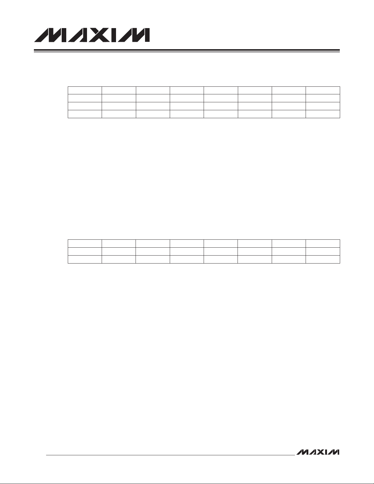
4.1.3 System Control Register (SC, M8[08h])
MAXQ Family User’s Guide:
MAXQ2010 Supplement
Bit #
Name TAP — — CDA0 — — PWL —
Reset 1 0 0 0 0 0 Unchanged 0
POR 1 0 0 0 0 0 1 0
Access rw r r r r r rw r
Bit 7: Test Access (Debug) Port Enable (TAP)
0 = Debug port functions are disabled, and P6.0 to P6.3 can be used as general-purpose I/O pins.
1 = Port pins P6.0 to P6.3 are enabled to act as debug port inputs and outputs.
Bits 6:5, 3:2, 0: Reserved
Bit 4: Code Data Access (CDA0). Setting this bit to 0 or 1 enables access to either the low or high page of program
memory in data space when accessing data in byte mode, as shown in Figure 2-3 and Figure 2-4. When accessing
data space in word mode, the setting of this bit has no effect.
Bit 1: Password Lock (PWL). This bit defaults to 1 on power-on reset only. When this bit is 1, it requires a 32-byte
password to be matched with the password in the program space (words 10h to 1Fh) before allowing access to the
ROM loader’s utilities for read/write of program memory and debug functions. Clearing this bit to 0 disables the password protection to the ROM loader.
7 6 5 4 3 2 1 0
4.1.4 Interrupt Identification Register (IIR, M8[0Bh])
Bit #
Name IIS — — II4 II3 II2 II1 II0
Reset 0 0 0 0 0 0 0 0
Access r r r r r r r r
7 6 5 4 3 2 1 0
The first four bits in this register indicate interrupts pending in modules 0 to 4, one bit per module. The eighth bit, IIS,
indicates a pending system interrupt (from the watchdog timer or other system function). The interrupt pending flags
are set only for enabled interrupt sources waiting for service. The interrupt pending flag is cleared when the pending
interrupt source(s) within that module are disabled or when the interrupt flag(s) are cleared by software.
Bit 7: Interrupt Pending Flag for System Modules (IIS)
Bits 6:5: Reserved
Bit 4: Interrupt Pending Flag for Module 4 (II4)
Bit 3: Interrupt Pending Flag for Module 3 (II3)
Bit 2: Interrupt Pending Flag for Module 2 (II2)
Bit 1: Interrupt Pending Flag for Module 1 (II1)
Bit 0: Interrupt Pending Flag for Module 0 (II0)
4-4
Page 31

MAXQ Family User’s Guide:
MAXQ2010 Supplement
4.1.5 System Clock Control Register (CKCN, M8[0Eh])
Bit #
Name — FLLSL FLLMD STOP SWB PMME CD1 CD0
Reset 1 Unchanged 0 0 0 0 0 0
POR 1 0 0 0 0 0 0 0
Access r rw s rw rw rw rw* rw*
*Unrestricted read access. This bit can only be modified when PMME = 0.
The CKCN register bit settings determine the system clock source and clock divider as described in Table 4-4.
Bit 7: Reserved
Bit 6: Frequency-Locked Loop Select (FLLSL)
0 = Selects the high-frequency oscillator as the system clock source.
1 = Selects the FLL as the system clock source.
Bit 5: Frequency-Locked Loop Mode (FLLMD). This read-only status bit indicates the clock source that is currently
being used.
0 = High-frequency oscillator is currently being used as the system clock source, because the FLL is not selected
(FLLSL = 0).
1 = FLL is currently being used as the system clock source. This is either because it is selected as the clock source
(FLLSL = 1), or because the high-frequency oscillator is in the process of warming up.
Bit 4: Stop-Mode Select (STOP). Setting this bit to 1 causes the processor to enter stop mode. This does not change
the currently selected clock-divide ratio.
Bit 3: Switchback Enable (SWB). Setting this bit to 1 enables switchback mode. If power-management mode (divide
by 256) is active and switchback is enabled, the PMME bit is cleared to 0 when any of the following conditions occurs.
• An external interrupt is generated based on an edge detect.
• Either serial port 0 or serial port 1 is enabled to receive data and detects a low condition on its data receive pin.
• Either serial port 0 or serial port 1 has a byte written to its buffer register by software.
• The SPI interface is enabled in master mode, and the SPIB register is written by software.
• The SPI interface is enabled is slave mode, and an external master drives the SSEL line low.
• A START condition occurs on the I2C bus, causing an I2C start interrupt to be generated.
• The power supply drops below the SVM threshold, causing an SVM interrupt to be generated.
• An ADC conversion is initiated by software by setting the ADCONV bit to 1.
• A time-of-day interrupt or subsecond alarm interrupt occurs from the RTC.
• Debug mode is entered through command entry or a breakpoint match (exits from PMM1 only).
Triggering a switchback condition only clears the PMME bit; the settings of CD0 and CD1 remain the same. When either
power-management mode is active, the SWB bit cannot be set to 1 as long as any of the above conditions are true.
Bit 2: Power-Management Mode Enable (PMME)
Bits 1:0: Clock Divide 1:0 (CD[1:0]). These three bits control the divide ratio or enable power-management mode for
the system clock as shown in Table 4-4. CD0 and CD1 can always be read, and they can be written as long as PMME
= 0.
Setting the PMME bit to 1 activates PMM mode, causing the system clock to be divided by 256. While PMME is set
to 1, CD0 and CD1 cannot be changed; their values determine the clock-divide ratio that is used when the processor
exits power-management mode.
7 6 5 4 3 2 1 0
4-5
Page 32

MAXQ Family User’s Guide:
MAXQ2010 Supplement
Table 4-4. System Clock Modes
FLLMD SWB PMME CD1 CD0 SYSTEM CLOCK SWITCHBACK
0 0 0 0 0 High-frequency clock/1 —
0 0 0 0 1 High-frequency clock/2 —
0 0 0 1 0 High-frequency clock/4 —
0 0 0 1 1 High-frequency clock/8 —
0 0 1 X X High-frequency clock/256 Not Active
0 1 1 X X High-frequency clock/256 Active
1 0 0 0 0 FLL clock/1 —
1 0 0 0 1 FLL clock/2 —
1 0 0 1 0 FLL clock/4 —
1 0 0 1 1 FLL clock/8 —
1 0 1 X X FLL clock/256 Not Active
1 1 1 X X FLL clock/256 Active
4-6
Page 33

MAXQ Family User’s Guide:
MAXQ2010 Supplement
ADDENDUM TO SECTION 5: PERIPHERAL REGISTER MODULES
Table 5-1. Peripheral Register Map
CYCLES
TO READ
1 1 00h PO0 PO4 MCNT
1 1 01h PO1 PO5
1 1 02h PO2 PO6
1 1 03h PO3
1 1 04h EIF0 EIF1
1 1 05h EIE0 EIE1
1 1 06h — EIF2 LCFG SCON1
1 1 07h — EIE2 — SBUF1
1 2 08h PI0 PI4
1 2 09h PI1 PI5
1 2 0Ah PI2 PI6
1 2 0Bh PI3 EIES1 LCD0
1 2 0Ch EIES0 EIES2 LCD1 I2CCN
1 2 0Dh —
1 2 0Eh — — LCD3 I2CTO
1 2 0Fh
2 2 10h PD0 PD4 LCD5 — — —
2 2 11h PD1 PD5 LCD6 — — —
2 2 12h PD2 PD6 LCD7 — — —
2 2 13h PD3 — LCD8 — — —
2 2 14h — — LCD9 — — —
2 2 15h — SPICN LCD10 — — —
2 2 16h — SPICF LCD11 — — —
2 2 17h — SPICK LCD12 — — —
2 2 18h RTRM — LCD13 — — —
2 2 19h
2 2 1Ah RTSS — LCD15 — — —
2 2 1Bh
2 2 1Ch
2 2 1Dh RSSA — LCD18 — — —
2 2 1Eh RASH — LCD19 — — —
2 2 1Fh
Note: Register names that appear in italics indicate registers in which all bits are read-only. Register names that appear in bold
indicate 16-bit registers. All other registers are 8 bits in width.
CYCLES
TO WRITE
REGISTER
INDEX
M0 M1 M2 M3 M4 M5
I2CBUF TB0R
MA I2CST TB0C
MB I2CIE TB1R
PWCN
RCNT
RTSH
RTSL
RASL
SPIB MC2
MC1
MC0
MC1R
MC0R PR0 TB0V
LCRA
SVM
— LCD4
— LCD14 — — —
— LCD16 — — —
— LCD17 — — —
— LCD20 — — —
LCD2
—
SCON0
SBUF0
SMD0
SMD1
PR1 TB1V
I2CCK TB2V
I2CSLA ADDATA
TB1C
TB2R
TB2C
ADST
ADADDR
TB0CN
TB1CN
TB2CN
ADCN
—
—
—
—
—
—
—
—
—
—
—
—
—
—
—
—
5-1
Page 34

MAXQ Family User’s Guide:
MAXQ2010 Supplement
Table 5-2. Peripheral Register Bit Functions
REG
PO0 PO0 (8 bits)
PO1 PO1 (8 bits)
PO2 PO2 (8 bits)
PO3 PO3 (8 bits)
EIF0 IE7 IE6 IE5 IE4 IE3 IE2 IE1 IE0
EIE0 EX7 EX6 EX5 EX4 EX3 EX2 EX1 EX0
PI0 PI0 (8 bits)
PI1 PI1 (8 bits)
PI2 PI2 (8 bits)
PI3 PI3 (8 bits)
EIES0 IT7 IT6 IT5 IT4 IT3 IT2 IT1 IT0
PWCN
PD0 PD0 (8 bits)
PD1 PD1 (8 bits)
PD2 PD2 (8 bits)
PD3 PD3 (8 bits)
RTRM TSGN TRM (7 bits)
RCNT WE — ACS — — — FT SQE ALSF ALDF RDYE RDY BUSY ASE ADE RTCE
RTSS RTSS (8 bits)
RTSH RTSH (16 bits)
RTSL RTSL (16 bits)
RSSA RSSA (8 bits)
RASH — — — — RASH (4 bits)
RASL RASL (8 bits)
PO4 PO4 (8 bits)
PO5 — PO5 (7 bits)
PO6 PO6 (8 bits)
SPIB SPIB (16 bits)
EIF1 — IE14 IE13 IE12 IE11 IE10 IE9 IE8
EIE1 — EX14 EX13 EX12 EX11 EX10 EX9 EX8
EIF2 IE22 IE21 IE20 IE19 IE18 IE17 IE16 IE15
EIE2 EX22 EX21 EX20 EX19 EX18 EX17 EX16 EX15
PI4 PI4 (8 bits)
PI5 — PI5 (7 bits)
PI6 PI6 (8 bits)
EIES1 — IT14 IT13 IT12 IT11 IT10 IT9 IT8
EIES2 IT22 IT21 IT20 IT19 IT18 IT17 IT16 IT15
SVM — — — — SVTH (4 bits) — — —
PD4 PD4 (8 bits)
PD5 — PD5 (7 bits)
PD6 PD6 (8 bits)
15 14 13 12 11 10 9 8 7 6 5 4 3 2 1 0
FREQMD
— — — — —
X32KMD
(2 bits)
BIT
BOD
REGEN
X32K
BYP
HFXD
SVM
STOP
X32K
X32D FLOCK FLLEN
RDY
SVMI SVMIE
SVM
RDY
SVMEN
5-2
Page 35

MAXQ Family User’s Guide:
MAXQ2010 Supplement
Table 5-2. Peripheral Register Bit Functions (continued)
I2CGCI
I2C
GCIE
I2C
GCEN
BIT
I2C
NACKI
NACKIE
SM0/
SM0/
I2C
STOP
MODFE
I2C
I2C
AD
I2C
I2CRXI I2CTXI I2CSRI
STRI
I2C
I2C
STRIE
RXIE
—
MODE
ADIDX (4 bits)
I2C
I2CAMI
I2CALI
I2C
I2C
ALIE
SM1 SM2 REN TB8 RB8 TI RI
FE
SM1 SM2 REN TB8 RB8 TI RI
FE
I2C
START
AD
CONV
I2C
AMIE
I2C
ACK
ADDAI
I2CTOI
TOIE
STRS
CFG
MSTM SPIEN
CKPHA
I2C
TXIE
I2C
MST
CKPOL
SRIE
I2CEN
REG
SPICN STBY SPIC ROVR WCOL MODF
SPICF ESPII — — — — CHR
SPICK SPICK (8 bits)
MCNT OF MCW CLD SQU OPCS MSUB MMAC SUS
MA MA (16 bits)
MB MB (16 bits)
MC2 MC2 (16 bits)
MC1 MC1 (16 bits)
MC0 MC0 (16 bits)
LCFG PCF4 PCF3 PCF2 PCF1 PCF0 SMO OPM DPE
MC1R MC1R (16 bits)
MC0R MC0R (16 bits)
LCRA — — — DUTY1 DUTY0 FRM3 FRM2 FRM1 FRM0 LCCS LRIG — LRA3 LRA2 LRA1 LRA0
LCD[n] LCD[n] (8 bits)
I2CBUF I2CBUF (16 bits)
I2CST
I2CIE — — — —
SCON0
SBUF0 SBUF0 (8 bits)
SCON1
SBUF1 SBUF1 (8 bits)
SMD0 — — — — — ESI SMOD FEDE
PR0 PR0 (16 bits)
SMD1 — — — — — ESI SMOD FEDE
PR1 PR1 (16 bits)
I2CCN
I2CCK I2CCKH (8 bits) I2CCKL (8 bits)
I2CTO I2CTO (8 bits)
I2CSLA — — — — — — I2CSLA (10 bits)
TB0R TB0R (16 bits)
TB0C TB0C (16 bits)
TB1R TB1R (16 bits)
TB1C TB1C (16 bits)
TB2R TB2R (16 bits)
TB2C TB2C (16 bits)
ADST — — — — ADDAT (4 bits) REFOK
ADADDR — — — — SEQSTORE (4 bits) — SEQSTART (3 bits) — SEQEND (3 bits)
15 14 13 12 11 10 9 8 7 6 5 4 3 2 1 0
I2C
BUS
I2C
RST
I2C
BUSY
— — I2CSPI
— — — — —
I2C
SPIE
I2CSCL
—
I2CROI
I2C
ROIE
I2C
STREN
I2C
5-3
Page 36

MAXQ Family User’s Guide:
MAXQ2010 Supplement
Table 5-2. Peripheral Register Bit Functions (continued)
REG
TB0CN C/TB — — TBCS TBCR TBPS (3 bits) TFB EXFB TBOE DCEN EXENB TRB ETB
TB0V TB0V (16 bits)
TB1CN C/TB — — TBCS TBCR TBPS (3 bits) TFB EXFB TBOE DCEN EXENB TRB ETB
TB1V TB1V (16 bits)
TB2CN C/TB — — TBCS TBCR TBPS (3 bits) TFB EXFB TBOE DCEN EXENB TRB ETB
TB2V TB2V (16 bits)
ADCN — — — — ADINT (2 bits)
ADDATA ADDATA (16 bits)
15 14 13 12 11 10 9 8 7 6 5 4 3 2 1 0
ADCLK
(2 bits)
Table 5-3. Peripheral Register Bit Reset Values
REG
PO0 1 1 1 1 1 1 1 1
PO1 1 1 1 1 1 1 1 1
PO2 1 1 1 1 1 1 1 1
PO3 1 1 1 1 1 1 1 1
EIF0 0 0 0 0 0 0 0 0
EIE0 0 0 0 0 0 0 0 0
PI0 s s s s s s s s
PI1 s s s s s s s s
PI2 s s s s s s s s
PI3 s s s s s s s s
EIES0 0 0 0 0 0 0 0 0
PWCN 0 0 0 0 0 0 0 0 0 0 0 0 s s 0 0
PD0 0 0 0 0 0 0 0 0
PD1 0 0 0 0 0 0 0 0
PD2 0 0 0 0 0 0 0 0
PD3 0 0 0 0 0 0 0 0
RTRM 0 0 0 0 0 0 0 0
RCNT 0 0 0 0 0 0 0 0 0 0 0 0 s 0 0 s
RTSS s s s s s s s s
RTSH s s s s s s s s s s s s s s s s
RTSL s s s s s s s s s s s s s s s s
RSSA 0 0 0 0 0 0 0 0
RASH 0 0 0 0 0 0 0 0
RASL 0 0 0 0 0 0 0 0 0 0 0 0 0 0 0 0
PO4 1 1 1 1 1 1 1 1
PO5 1 1 1 1 1 1 1 1
PO6 1 1 1 1 1 1 1 1
15 14 13 12 11 10 9 8 7 6 5 4 3 2 1 0
BIT
IREFENAD
BIT
CONTADDAIEADPMO
ADACQ (4 bits)
CP/
RLB
CP/
RLB
CP/
RLB
5-4
Page 37

MAXQ Family User’s Guide:
MAXQ2010 Supplement
Table 5-3. Peripheral Register Bit Reset Values (continued)
REG
SPIB 0 0 0 0 0 0 0 0 0 0 0 0 0 0 0 0
EIF1 0 0 0 0 0 0 0 0
EIE1 0 0 0 0 0 0 0 0
EIF2 0 0 0 0 0 0 0 0
EIE2 0 0 0 0 0 0 0 0
PI4 s s s s s s s s
PI5 0 s s s s s s s
PI6 s s s s s s s s
EIES1 0 0 0 0 0 0 0 0
EIES2 0 0 0 0 0 0 0 0
SVM 0 0 0 0 0 1 1 1 0 0 0 0 0 0 0 0
PD4 0 0 0 0 0 0 0 0
PD5 0 0 0 0 0 0 0 0
PD6 0 0 0 0 0 0 0 0
SPICN 0 0 0 0 0 0 0 0
SPICF 0 0 0 0 0 0 0 0
SPICK 0 0 0 0 0 0 0 0
MCNT 0 0 0 0 0 0 0 0
MA 0 0 0 0 0 0 0 0 0 0 0 0 0 0 0 0
MB 0 0 0 0 0 0 0 0 0 0 0 0 0 0 0 0
MC2 0 0 0 0 0 0 0 0 0 0 0 0 0 0 0 0
MC1 0 0 0 0 0 0 0 0 0 0 0 0 0 0 0 0
MC0 0 0 0 0 0 0 0 0 0 0 0 0 0 0 0 0
LCFG 0 0 0 0 0 0 0 0
MC1R 0 0 0 0 0 0 0 0 0 0 0 0 0 0 0 0
MC0R 0 0 0 0 0 0 0 0 0 0 0 0 0 0 0 0
LCRA 0 0 0 0 0 0 0 0 0 0 0 0 0 0 0 0
LCD[n] 0 0 0 0 0 0 0 0
I2CBUF 0 0 0 0 0 0 0 0 0 0 0 0 0 0 0 0
I2CST 0 0 0 0 0 0 0 0 0 0 0 0 0 0 0 0
I2CIE 0 0 0 0 0 0 0 0 0 0 0 0 0 0 0 0
SCON0 0 0 0 0 0 0 0 0
SBUF0 0 0 0 0 0 0 0 0
SCON1 0 0 0 0 0 0 0 0
SBUF1 0 0 0 0 0 0 0 0
SMD0 0 0 0 0 0 0 0 0
PR0 0 0 0 0 0 0 0 0 0 0 0 0 0 0 0 0
SMD1 0 0 0 0 0 0 0 0
PR1 0 0 0 0 0 0 0 0 0 0 0 0 0 0 0 0
I2CCN 0 0 0 0 0 0 0 0 0 0 0 0 0 0 0 0
I2CCK 0 0 0 0 0 0 1 0 0 0 0 0 0 1 0 0
I2CTO 0 0 0 0 0 0 0 0
I2CSLA 0 0 0 0 0 0 0 0 0 0 0 0 0 0 0 0
TB0R 0 0 0 0 0 0 0 0 0 0 0 0 0 0 0 0
15 14 13 12 11 10 9 8 7 6 5 4 3 2 1 0
BIT
5-5
Page 38

MAXQ Family User’s Guide:
MAXQ2010 Supplement
Table 5-3. Peripheral Register Bit Reset Values (continued)
REG
TB0C 0 0 0 0 0 0 0 0 0 0 0 0 0 0 0 0
TB1R 0 0 0 0 0 0 0 0 0 0 0 0 0 0 0 0
TB1C 0 0 0 0 0 0 0 0 0 0 0 0 0 0 0 0
TB2R 0 0 0 0 0 0 0 0 0 0 0 0 0 0 0 0
TB2C 0 0 0 0 0 0 0 0 0 0 0 0 0 0 0 0
ADST 0 0 0 0 0 0 0 0 0 0 0 0 0 0 0 0
ADADDR 0 0 0 0 0 0 0 0 0 0 0 0 0 0 0 0
TB0CN 0 0 0 0 0 0 0 0 0 0 0 0 0 0 0 0
TB0V 0 0 0 0 0 0 0 0 0 0 0 0 0 0 0 0
TB1CN 0 0 0 0 0 0 0 0 0 0 0 0 0 0 0 0
TB1V 0 0 0 0 0 0 0 0 0 0 0 0 0 0 0 0
TB2CN 0 0 0 0 0 0 0 0 0 0 0 0 0 0 0 0
TB2V 0 0 0 0 0 0 0 0 0 0 0 0 0 0 0 0
ADCN 0 0 0 0 0 0 0 0 0 0 0 0 0 0 0 0
ADDATA s s s s s s s s s s s s s s s s
Note: Bits marked as “s” have special behavior upon reset; see the register descriptions for details.
15 14 13 12 11 10 9 8 7 6 5 4 3 2 1 0
BIT
5-6
Page 39

MAXQ Family User’s Guide:
MAXQ2010 Supplement
ADDENDUM TO SECTION 6: GENERAL-PURPOSE I/O MODULE
The MAXQ2010 provides up to 55 port pins for general-purpose I/O that are grouped into logical ports P0 to P6. Each
of these port pins has the following features:
• CMOS output drivers
• Schmitt trigger inputs
• Optional weak pullup to DVDD when operating in input mode
Many of the port pins on the MAXQ2010 are also multiplexed with special and alternate functions as listed below.
All these functions are disabled by default with the exception of the debug port interface pins, which are enabled by
default following any reset. The behavior of these functions breaks down into two overall categories.
• Special functions override the PD and PO settings for the port pin when they are enabled. Once the special function takes control, normal control of the port pin is lost until the special function completes its task or is disabled.
Examples of special functions include serial port 0 transmit and LCD segment drive.
• Alternate functions operate in parallel with the PD and PO settings for the port pin, and generally consist of input-
only functions such as external interrupts. When an alternate function is enabled for a port pin, the port pin’s output
state is still controlled in the usual manner.
Table 6-1. Port Pin Special and Alternate Functions
PORT PIN FUNCTION TYPE FUNCTION ENABLED WHEN
P0.0 Special Analog LCD Segment SEG0 DPE = 1, PCF0 = 1, and EX0 = 0
P0.0 Alternate External Interrupt 0 (EIE0.0) EX0 = 1
P0.1 Special Analog LCD Segment SEG1 DPE = 1, PCF0 = 1, and EX1 = 0
P0.1 Alternate External Interrupt 1 (EIE0.1) EX1 = 1
P0.2 Special Analog LCD Segment SEG2 DPE = 1, PCF0 = 1, and EX2 = 0
P0.2 Alternate External Interrupt 2 (EIE0.2) EX2 = 1
P0.3 Special Analog LCD Segment SEG3 DPE = 1, PCF0 = 1, and EX3 = 0
P0.3 Alternate External Interrupt 3 (EIE0.3) EX3 = 1
P0.4 Special Analog LCD Segment SEG4 DPE = 1, PCF0 = 1, and EX4 = 0
P0.4 Alternate External Interrupt 4 (EIE0.4) EX4 = 1
P0.5 Special Analog LCD Segment SEG5 DPE = 1, PCF0 = 1, and EX5 = 0
P0.5 Alternate External Interrupt 5 (EIE0.5) EX5 = 1
P0.6 Special Analog LCD Segment SEG6 DPE = 1, PCF0 = 1, and EX6 = 0
P0.6 Alternate External Interrupt 6 (EIE0.6) EX6 = 1
P0.7 Special Analog LCD Segment SEG7 DPE = 1, PCF0 = 1, and EX7 = 0
P0.7 Alternate External Interrupt 7 (EIE0.7) EX7 = 1
P1.0 Special Analog LCD Segment SEG8 DPE = 1 and PCF1 = 1
P1.1 Special Analog LCD Segment SEG9 DPE = 1 and PCF1 = 1
P1.2 Special Analog LCD Segment SEG10 DPE = 1 and PCF1 = 1
P1.3 Special Analog LCD Segment SEG11 DPE = 1 and PCF1 = 1
P1.4 Special Analog LCD Segment SEG12 DPE = 1 and PCF1 = 1
P1.5 Special Analog LCD Segment SEG13 DPE = 1 and PCF1 = 1
P1.6 Special Analog LCD Segment SEG14 DPE = 1 and PCF1 = 1
P1.7 Special Analog LCD Segment SEG15 DPE = 1 and PCF1 = 1
P2.0 Special Analog LCD Segment SEG16 DPE = 1 and PCF2 = 1
P2.1 Special Analog LCD Segment SEG17 DPE = 1 and PCF2 = 1
P2.2 Special Analog LCD Segment SEG18 DPE = 1 and PCF2 = 1
6-1
Page 40

MAXQ Family User’s Guide:
MAXQ2010 Supplement
Table 6-1. Port Pin Special and Alternate Functions (continued)
PORT PIN FUNCTION TYPE FUNCTION ENABLED WHEN
P2.3 Special Analog LCD Segment SEG19 DPE = 1 and PCF2 = 1
P2.4 Special Analog LCD Segment SEG20 DPE = 1 and PCF2 = 1
P2.5 Special Analog LCD Segment SEG21 DPE = 1 and PCF2 = 1
P2.6 Special Analog LCD Segment SEG22 DPE = 1 and PCF2 = 1
P2.7 Special Analog LCD Segment SEG23 DPE = 1 and PCF2 = 1
P3.0 Special Analog LCD Segment SEG24 DPE = 1 and PCF3 = 1
P3.1 Special Analog LCD Segment SEG25 DPE = 1 and PCF3 = 1
P3.2 Special Analog LCD Segment SEG26 DPE = 1 and PCF3 = 1
P3.3 Special Analog LCD Segment SEG27 DPE = 1 and PCF3 = 1
P3.4 Special Analog LCD Segment SEG28 DPE = 1 and PCF3 = 1
P3.5 Special Analog LCD Segment SEG29 DPE = 1 and PCF3 = 1
P3.6 Special Analog LCD Segment SEG30 DPE = 1 and PCF3 = 1
P3.7 Special Analog LCD Segment SEG31 DPE = 1 and PCF3 = 1
P4.0 Special Analog LCD Segment SEG32 DPE = 1 and PCF4 = 1
P4.1 Special Analog LCD Segment SEG33 DPE = 1 and PCF4 = 1
P4.2 Special Analog LCD Segment SEG34 DPE = 1 and PCF4 = 1
P4.3 Special Analog LCD Segment SEG35 DPE = 1 and PCF4 = 1
P4.4 Special Analog LCD Segment SEG36 DPE = 1 and PCF4 = 1
P4.5 Special Analog LCD Segment SEG37 DPE = 1 and PCF4 = 1
P4.6 Special Analog LCD Segment SEG38 DPE = 1 and PCF4 = 1
P4.7 Special Analog LCD Segment SEG39 DPE = 1 and PCF4 = 1
P5.0 Alternate External Interrupt 8 (EIE1.0) EX8 = 1
P5.0 Alternate Type B Timer 0 Input B EXENB = 1
P5.0 Special Type B Timer 0 Output B (Compare Output)
P5.0 Special Serial Port 0 Data (Mode 0)
P5.0 Alternate Serial Port 0 Receive (Modes 1/2/3) Modes 1/2/3: REN = 1
P5.1 Alternate External Interrupt 9 (EIE1.1) EX9 = 1
P5.1 Alternate Type B Timer 0 Input A (Counter Input) C/TB = 1
P5.1 Special Type B Timer 0 Output A (Clock Output)
P5.1 Special Serial Port 0 Transmit/Clock
P5.2 Alternate External Interrupt 10 (EIE1.2) EX10 = 1
P5.2 Special RTC Square-Wave Output RTCE = 1 and SQE = 1
P5.3 Alternate External Interrupt 11 (EIE1.3) EX11 = 1
P5.3 Alternate
P5.4 Alternate External Interrupt 12 (EIE1.4) EX12 = 1
P5.4 Alternate MOSI: SPI Slave Input (Slave Mode) SPIEN = 1 and MSTM = 0
P5.4 Special MOSI: SPI Master Output (Master Mode) SPIEN = 1 and MSTM = 1
P5.5 Alternate External Interrupt 13 (EIE1.5) EX13 = 1
P5.5 Alternate SCLK: SPI Clock Input (Slave Mode) SPIEN = 1 and MSTM = 0
SPI Slave-Select Input (SSEL)
TBCR:TBCS<>00b
(overrides Serial 0 Data)
Mode 0: SBUF0 is written or REN is set to 1
(until serial transmission completes)
C/TB = 0 and TB0E = 1 (overrides serial
port 0 transmit/clock)
Mode 0: REN set to 1 (until serial transmission completes)
Mode 1/2/3: SBUF0 is written (until serial
transmission completes)
SPIEN = 1 and MSTM = 0
6-2
Page 41

MAXQ Family User’s Guide:
MAXQ2010 Supplement
Table 6-1. Port Pin Special and Alternate Functions (continued)
PORT PIN FUNCTION TYPE FUNCTION ENABLED WHEN
P5.5 Special SCLK: SPI Clock Output (Master Mode) SPIEN = 1 and MSTM = 1
P5.6 Alternate External Interrupt 14 (EIE1.6) EX14 = 1
P5.6 Special MISO: SPI Slave Output (Slave Mode) SPIEN = 1 and MSTM = 0
P5.6 Alternate MISO: SPI Master Input (Master Mode) SPIEN = 1 and MSTM = 1
P6.0 Alternate JTAG Interface: TAP Clock (TCK) (SC.7) TAP = 1
P6.0 Alternate External Interrupt 15 (EIE2.0) EX15 = 1
P6.1 Alternate JTAG Interface: TAP Data Input (TDI) (SC.7) TAP = 1
P6.1 Alternate External Interrupt 16 (EIE2.1) EX16 = 1
P6.2 Alternate JTAG Interface: TAP Mode Select (TMS) (SC.7) TAP = 1
P6.2 Alternate External Interrupt 17 (EIE2.2) EX17 = 1
P6.3 Special JTAG Interface: TAP Data Output (TDO) (SC.7) TAP = 1
P6.3 Alternate External Interrupt 18 (EIE2.3) EX18 = 1
P6.4 Alternate External Interrupt 19 (EIE2.4) EX19 = 1
P6.4 Alternate Type B Timer 1 Input B EXENB = 1
P6.4 Special Type B Timer 1 Output B (Compare Output)
P6.4 Special Serial Port 1 Data (Mode 0)
P6.4 Alternate Serial Port 1 Receive (Modes 1/2/3) Modes 1/2/3: REN = 1
P6.5 Alternate External Interrupt 20 (EIE2.5) EX20 = 1
P6.5 Alternate Type B Timer 0 Input A (Counter Input) C/TB = 1
P6.5 Special Type B Timer 0 Output A (Clock Output)
P6.5 Special Serial Port 1 Transmit/Clock
P6.6 Alternate External Interrupt 21 (EIE2.6) EX21 = 1
P6.6 Alternate Type B Timer 2 Input B EXENB = 1
P6.6 Special Type B Timer 2 Output B (Compare Output) TBCR:TBCS<>00b
P6.6 Special SCL: I2C Clock Line
P6.7 Alternate External Interrupt 22 (EIE2.7) EX22 = 1
P6.7 Alternate Type B Timer 0 Input A (Counter Input) C/TB = 1
P6.7 Special Type B Timer 0 Output A (Clock Output) C/TB = 0 and TB0E = 1
P6.7 Special SDA: I2C Data Line
TBCR:TBCS<>00b
(overrides serial port 1 data)
Mode 0: SBUF1 is written or REN is set to 1
(until serial transmission completes)
C/TB = 0 and TB0E = 1
(overrides serial port 1 transmit/clock)
Mode 0: REN set to 1 (until serial transmission completes)
Mode 1/2/3: SBUF1 is written (until serial
transmission completes)
I2CEN = 1
(overrides timer B output B)
I2CEN = 1
(overrides timer B output A)
6-3
Page 42

MAXQ Family User’s Guide:
MAXQ2010 Supplement
The port pins on the MAXQ2010 operate the same as standard MAXQ port pins, with input/output states defined in
Table 6-2.
Table 6-2. Port Pin Input/Output States (in Standard Mode)
PDx.y POx.y PORT PIN MODE PORT PIN (Px.y) STATE
0 0 Input Three-State
0 1 Input Weak pullup high
1 0 Output Strong drive low
1 1 Output Strong drive high
6.1 GPIO and External Interrupt Register Descriptions
The following peripheral registers are used to control the general-purpose I/O and external interrupt features specific
to the MAXQ2010. Addresses of registers are given as “Mx[yy],” where x is the module number (from 0 to 15 decimal)
and yy is the register index (from 00h to 1Fh hexadecimal). Fields in the bit definition tables are defined as follows:
• Name: Symbolic names of bits or bit fields in this register.
• Reset: The value of each bit in this register following a standard reset. If this field reads “unchanged,” the given bit
is unaffected by standard reset. If this field reads “s,” the given bit does not have a fixed 0 or 1 reset value because
its value is determined by another internal state or external condition.
• POR: If present this field defines the value of each bit in this register following a power-on reset (as opposed to a
standard reset). Some bits are unaffected by standard resets and are set/cleared by POR only.
• Access: Bits can be read-only (r) or read/write (rw). Any special restrictions or conditions that could apply when
reading or writing this bit are detailed in the bit description.
6.1.1 Port 0 Direction Register (PD0, M0[10h])
Bit #
Name PD0
Reset 0 0 0 0 0 0 0 0
Access rw rw rw rw rw rw rw rw
Each of the bits in this register controls the input/output direction of a port pin (P0.0 to P0.7) as follows:
0 = The port pin is in input mode, either with a weak pullup (if PO = 1) or three-stated (if PO = 0).
1 = The port pin is in output mode, with the output level to drive given by PO.
7 6 5 4 3 2 1 0
6.1.2 Port 1 Direction Register (PD1, M0[11h])
Bit #
Name PD1
Reset 0 0 0 0 0 0 0 0
Access rw rw rw rw rw rw rw rw
Each of the bits in this register controls the input/output direction of a port pin (P1.0 to P1.7) as follows:
0 = The port pin is in input mode, either with a weak pullup (if PO = 1) or three-stated (if PO = 0).
1 = The port pin is in output mode, with the output level to drive given by PO.
7 6 5 4 3 2 1 0
6-4
Page 43

MAXQ Family User’s Guide:
MAXQ2010 Supplement
6.1.3 Port 2 Direction Register (PD2, M0[12h])
Bit #
Name PD2
Reset 0 0 0 0 0 0 0 0
Access rw rw rw rw rw rw rw rw
Each of the bits in this register controls the input/output direction of a port pin (P2.0 to P2.7) as follows:
0 = The port pin is in input mode, either with a weak pullup (if PO = 1) or three-stated (if PO = 0).
1 = The port pin is in output mode, with the output level to drive given by PO.
6.1.4 Port 3 Direction Register (PD3, M0[13h])
Bit #
Name PD3
Reset 0 0 0 0 0 0 0 0
Access rw rw rw rw rw rw rw rw
Each of the bits in this register controls the input/output direction of a port pin (P3.0 to P3.7) as follows:
0 = The port pin is in input mode, either with a weak pullup (if PO = 1) or three-stated (if PO = 0).
1 = The port pin is in output mode, with the output level to drive given by PO.
7 6 5 4 3 2 1 0
7 6 5 4 3 2 1 0
6.1.5 Port 4 Direction Register (PD4, M1[10h])
Bit #
Name PD4
Reset 0 0 0 0 0 0 0 0
Access rw rw rw rw rw rw rw rw
Each of the bits in this register controls the input/output direction of a port pin (P4.0 to P4.7) as follows:
0 = The port pin is in input mode, either with a weak pullup (if PO = 1) or three-stated (if PO = 0).
1 = The port pin is in output mode, with the output level to drive given by PO.
7 6 5 4 3 2 1 0
6-5
Page 44

6.1.6 Port 5 Direction Register (PD5, M1[11h])
MAXQ Family User’s Guide:
MAXQ2010 Supplement
Bit #
Name — PD5
Reset 0 0 0 0 0 0 0 0
Access r rw rw rw rw rw rw rw
Each of the bits in this register controls the input/output direction of a port pin (P5.0 to P5.6) as follows:
0 = The port pin is in input mode, either with a weak pullup (if PO = 1) or three-stated (if PO = 0).
1 = The port pin is in output mode, with the output level to drive given by PO.
7 6 5 4 3 2 1 0
6.1.7 Port 6 Direction Register (PD6, M1[12h])
Bit #
Name PD6
Reset 0 0 0 0 0 0 0 0
Access rw rw rw rw rw rw rw rw
Each of the bits in this register controls the input/output direction of a port pin (P6.0 to P6.7) as follows:
0 = The port pin is in input mode, either with a weak pullup (if PO = 1) or three-stated (if PO = 0).
1 = The port pin is in output mode, with the output level to drive given by PO.
7 6 5 4 3 2 1 0
6.1.8 Port 0 Output Register (PO0, M0[00h])
Bit #
Name PO0
Reset 1 1 1 1 1 1 1 1
Access rw rw rw rw rw rw rw rw
7 6 5 4 3 2 1 0
Bits 7:0: Port 0 Output. This register stores the data that is output on any of the pins of port 0 that have been defined
as output pins. If the port pins are in input mode, this register controls the weak pullup for each pin. Changing the data
direction of any pins for this port (through register PD0) does not affect the value in this register.
6.1.9 Port 1 Output Register (PO1, M0[01h])
Bit #
Name PO1
Reset 1 1 1 1 1 1 1 1
Access rw rw rw rw rw rw rw rw
Bits 7:0: Port 1 Output. This register stores the data that is output on any of the pins of port 1 that have been defined
as output pins. If the port pins are in input mode, this register controls the weak pullup for each pin. Changing the data
direction of any pins for this port (through register PD1) does not affect the value in this register.
6-6
7 6 5 4 3 2 1 0
Page 45

MAXQ Family User’s Guide:
MAXQ2010 Supplement
6.1.10 Port 2 Output Register (PO2, M0[02h])
Bit #
Name PO2
Reset 1 1 1 1 1 1 1 1
Access rw rw rw rw rw rw rw rw
Bits 7:0: Port 2 Output. This register stores the data that is output on any of the pins of port 2 that have been defined
as output pins. If the port pins are in input mode, this register controls the weak pullup for each pin. Changing the data
direction of any pins for this port (through register PD2) does not affect the value in this register.
7 6 5 4 3 2 1 0
6.1.11 Port 3 Output Register (PO3, M0[03h])
Bit #
Name PO3
Reset 1 1 1 1 1 1 1 1
Access rw rw rw rw rw rw rw rw
Bits 7:0: Port 3 Output. This register stores the data that is output on any of the pins of port 3 that have been defined
as output pins. If the port pins are in input mode, this register controls the weak pullup for each pin. Changing the data
direction of any pins for this port (through register PD3) does not affect the value in this register.
7 6 5 4 3 2 1 0
6.1.12 Port 4 Output Register (PO4, M1[00h])
Bit #
Name PO4
Reset 1 1 1 1 1 1 1 1
Access rw rw rw rw rw rw rw rw
7 6 5 4 3 2 1 0
Bits 7:0: Port 4 Output. This register stores the data that is output on any of the pins of port 4 that have been defined
as output pins. If the port pins are in input mode, this register controls the weak pullup for each pin. Changing the data
direction of any pins for this port (through register PD4) does not affect the value in this register.
6.1.13 Port 5 Output Register (PO5, M1[01h])
Bit #
Name — PO5
Reset 1 1 1 1 1 1 1 1
Access r rw rw rw rw rw rw rw
Bits 7:0: Port 5 Output. This register stores the data that is output on any of the pins of port 5 that have been defined
as output pins. If the port pins are in input mode, this register controls the weak pullup for each pin. Changing the data
direction of any pins for this port (through register PD5) does not affect the value in this register.
7 6 5 4 3 2 1 0
6-7
Page 46
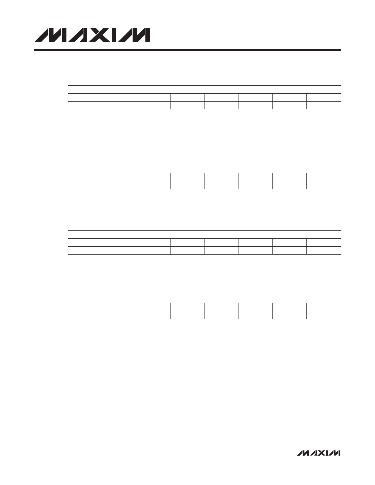
MAXQ Family User’s Guide:
MAXQ2010 Supplement
6.1.14 Port 6 Output Register (PO6, M1[02h])
Bit #
Name PO6
Reset 1 1 1 1 1 1 1 1
Access rw rw rw rw rw rw rw rw
Bits 7:0: Port 6 Output. This register stores the data that is output on any of the pins of port 6 that have been defined
as output pins. If the port pins are in input mode, this register controls the weak pullup for each pin. Changing the data
direction of any pins for this port (through register PD6) does not affect the value in this register.
6.1.15 Port 0 Input Register (PI0, M0[08h])
7 6 5 4 3 2 1 0
Bit #
Name PI0
Reset s s s s s s s s
Access r r r r r r r r
Each of the read-only bits in this register reflects the logic state present at the corresponding port pin.
7 6 5 4 3 2 1 0
6.1.16 Port 1 Input Register (PI1, M0[09h])
Bit #
Name PI1
Reset s s s s s s s s
Access r r r r r r r r
Each of the read-only bits in this register reflects the logic state present at the corresponding port pin.
7 6 5 4 3 2 1 0
6.1.17 Port 2 Input Register (PI2, M0[0Ah])
Bit #
Name PI2
Reset s s s s s s s s
Access r r r r r r r r
Each of the read-only bits in this register reflects the logic state present at the corresponding port pin.
7 6 5 4 3 2 1 0
6-8
Page 47

MAXQ Family User’s Guide:
MAXQ2010 Supplement
6.1.18 Port 3 Input Register (PI3, M0[0Bh])
Register Name
Register Description Port 3 Input Register
Register Address M0[0Bh]
Bit #
Name PI3
Reset s s s s s s s s
Access r r r r r r r r
7 6 5 4 3 2 1 0
PI3
Each of the read-only bits in this register reflects the logic state present at the corresponding port pin.
6.1.19 Port 4 Input Register (PI4, M1[08h])
Bit #
Name PI4
Reset s s s s s s s s
Access r r r r r r r r
Each of the read-only bits in this register reflects the logic state present at the corresponding port pin.
7 6 5 4 3 2 1 0
6.1.20 Port 5 Input Register (PI5, M1[09h])
Bit #
Name — PI5
Reset 0 s s s s s s s
Access r r r r r r r r
7 6 5 4 3 2 1 0
Each of the read-only bits in this register reflects the logic state present at the corresponding port pin.
6.1.21 Port 6 Input Register (PI6, M1[0Ah])
Bit #
Name PI6
Reset s s s s s s s s
Access r r r r r r r r
Each of the read-only bits in this register reflects the logic state present at the corresponding port pin.
7 6 5 4 3 2 1 0
6-9
Page 48

MAXQ Family User’s Guide:
6.1.22 External Interrupt Flag 0 Register (EIF0, M0[04h])
MAXQ2010 Supplement
Bit #
Name IE7 IE6 IE5 IE4 IE3 IE2 IE1 IE0
Reset 0 0 0 0 0 0 0 0
Access rw rw rw rw rw rw rw rw
Each bit in this register is set when a negative or positive edge (depending on the ITn bit setting) is detected on the corresponding interrupt pin. Once an external interrupt has been detected, the interrupt flag bit remains set until cleared
by software or a reset. Setting any of these bits causes the corresponding interrupt to trigger if it is enabled to do so.
Bit 7: External Interrupt 7 Edge Detect (IE7)
Bit 6: External Interrupt 6 Edge Detect (IE6)
Bit 5: External Interrupt 5 Edge Detect (IE5)
Bit 4: External Interrupt 4 Edge Detect (IE4)
Bit 3: External Interrupt 3 Edge Detect (IE3)
Bit 2: External Interrupt 2 Edge Detect (IE2)
Bit 1: External Interrupt 1 Edge Detect (IE1)
Bit 0: External Interrupt 0 Edge Detect (IE0)
7 6 5 4 3 2 1 0
6.1.23 External Interrupt Flag 1 Register (EIF1, M1[04h])
Bit #
Name — IE14 IE13 IE12 IE11 IE10 IE9 IE8
Reset 0 0 0 0 0 0 0 0
Access r rw rw rw rw rw rw rw
7 6 5 4 3 2 1 0
Each bit in this register is set when a negative or positive edge (depending on the ITn bit setting) is detected on the corresponding interrupt pin. Once an external interrupt has been detected, the interrupt flag bit remains set until cleared
by software or a reset. Setting any of these bits causes the corresponding interrupt to trigger if it is enabled to do so.
Bit 7: Reserved
Bit 6: External Interrupt 14 Edge Detect (IE14)
Bit 5: External Interrupt 13 Edge Detect (IE13)
Bit 4: External Interrupt 12 Edge Detect (IE12)
Bit 3: External Interrupt 11 Edge Detect (IE11)
Bit 2: External Interrupt 10 Edge Detect (IE10)
Bit 1: External Interrupt 9 Edge Detect (IE9)
Bit 0: External Interrupt 8 Edge Detect (IE8)
6-10
Page 49

MAXQ Family User’s Guide:
MAXQ2010 Supplement
6.1.24 External Interrupt Flag 2 Register (EIF2, M1[06h])
Bit #
Name IE22 IE21 IE20 IE19 IE18 IE17 IE16 IE15
Reset 0 0 0 0 0 0 0 0
Access rw rw rw rw rw rw rw rw
Each bit in this register is set when a negative or positive edge (depending on the ITn bit setting) is detected on the corresponding interrupt pin. Once an external interrupt has been detected, the interrupt flag bit remains set until cleared
by software or a reset. Setting any of these bits causes the corresponding interrupt to trigger if it is enabled to do so.
Bit 7: External Interrupt 22 Edge Detect (IE22)
Bit 6: External Interrupt 21 Edge Detect (IE21)
Bit 5: External Interrupt 20 Edge Detect (IE20)
Bit 4: External Interrupt 19 Edge Detect (IE19)
Bit 3: External Interrupt 18 Edge Detect (IE18)
Bit 2: External Interrupt 17 Edge Detect (IE17)
Bit 1: External Interrupt 16 Edge Detect (IE16)
Bit 0: External Interrupt 15 Edge Detect (IE15)
7 6 5 4 3 2 1 0
6.1.25 External Interrupt Enable 0 Register (EIE0, M0[05h])
Bit #
Name EX7 EX6 EX5 EX4 EX3 EX2 EX1 EX0
Reset 0 0 0 0 0 0 0 0
Access rw rw rw rw rw rw rw rw
7 6 5 4 3 2 1 0
Each bit in this register controls the enable for one external interrupt. If the bit is set to 1, the interrupt is enabled (if it
is not otherwise masked). If the bit is set to 0, its corresponding interrupt is disabled.
Bit 7: External Interrupt 7 Enable (EX7)
Bit 6: External Interrupt 6 Enable (EX6)
Bit 5: External Interrupt 5 Enable (EX5)
Bit 4: External Interrupt 4 Enable (EX4)
Bit 3: External Interrupt 3 Enable (EX3)
Bit 2: External Interrupt 2 Enable (EX2)
Bit 1: External Interrupt 1 Enable (EX1)
Bit 0: External Interrupt 0 Enable (EX0)
6-11
Page 50

MAXQ Family User’s Guide:
MAXQ2010 Supplement
6.1.26 External Interrupt Enable 1 Register (EIE1, M1[05h])
Bit #
Name — EX14 EX13 EX12 EX11 EX10 EX9 EX8
Reset 0 0 0 0 0 0 0 0
Access r rw rw rw rw rw rw rw
Each bit in this register controls the enable for one external interrupt. If the bit is set to 1, the interrupt is enabled (if it
is not otherwise masked). If the bit is set to 0, its corresponding interrupt is disabled.
Bit 7: Reserved
Bit 6: External Interrupt 14 Enable (EX14)
Bit 5: External Interrupt 13 Enable (EX13)
Bit 4: External Interrupt 12 Enable (EX12)
Bit 3: External Interrupt 11 Enable (EX11)
Bit 2: External Interrupt 10 Enable (EX10)
Bit 1: External Interrupt 9 Enable (EX9)
Bit 0: External Interrupt 8 Enable (EX8)
7 6 5 4 3 2 1 0
6.1.27 External Interrupt Enable 2 Register (EIE2, M1[07h])
Bit #
Name EX22 EX21 EX20 EX19 EX18 EX17 EX16 EX15
Reset 0 0 0 0 0 0 0 0
Access rw rw rw rw rw rw rw rw
7 6 5 4 3 2 1 0
Each bit in this register controls the enable for one external interrupt. If the bit is set to 1, the interrupt is enabled (if it
is not otherwise masked). If the bit is set to 0, its corresponding interrupt is disabled.
Bit 7: External Interrupt 22 Enable (EX22)
Bit 6: External Interrupt 21 Enable (EX21)
Bit 5: External Interrupt 20 Enable (EX20)
Bit 4: External Interrupt 19 Enable (EX19)
Bit 3: External Interrupt 18 Enable (EX18)
Bit 2: External Interrupt 17 Enable (EX17)
Bit 1: External Interrupt 16 Enable (EX16)
Bit 0: External Interrupt 15 Enable (EX15)
6-12
Page 51

MAXQ Family User’s Guide:
MAXQ2010 Supplement
6.1.28 External Interrupt Edge Select 0 Register (EIES0, M0[0Ch])
Bit #
Name IT7 IT6 IT5 IT4 IT3 IT2 IT1 IT0
Reset 0 0 0 0 0 0 0 0
Access rw rw rw rw rw rw rw rw
Each bit in this register controls the edge select mode for an external interrupt as follows:
0 = The external interrupt triggers on a rising (positive) edge.
1 = The external interrupt triggers on a negative (falling) edge.
Bit 7: Edge Select for External Interrupt 7 (IT7)
Bit 6: Edge Select for External Interrupt 6 (IT6)
Bit 5: Edge Select for External Interrupt 5 (IT5)
Bit 4: Edge Select for External Interrupt 4 (IT4)
Bit 3: Edge Select for External Interrupt 3 (IT3)
Bit 2: Edge Select for External Interrupt 2 (IT2)
Bit 1: Edge Select for External Interrupt 1 (IT1)
Bit 0: Edge Select for External Interrupt 0 (IT0)
7 6 5 4 3 2 1 0
6.1.29 External Interrupt Edge Select 1 Register (EIES1, M1[0Bh])
Bit #
Name — IT14 IT13 IT12 IT11 IT10 IT9 IT8
Reset 0 0 0 0 0 0 0 0
Access r rw rw rw rw rw rw rw
7 6 5 4 3 2 1 0
Each bit in this register controls the edge select mode for an external interrupt as follows:
0 = The external interrupt triggers on a rising (positive) edge.
1 = The external interrupt triggers on a negative (falling) edge.
Bit 7: Reserved
Bit 6: Edge Select for External Interrupt 14 (IT14)
Bit 5: Edge Select for External Interrupt 13 (IT13)
Bit 4: Edge Select for External Interrupt 12 (IT12)
Bit 3: Edge Select for External Interrupt 11 (IT11)
Bit 2: Edge Select for External Interrupt 10 (IT10)
Bit 1: Edge Select for External Interrupt 9 (IT9)
Bit 0: Edge Select for External Interrupt 8 (IT8)
6-13
Page 52

MAXQ Family User’s Guide:
MAXQ2010 Supplement
6.1.30 External Interrupt Edge Select 2 Register (EIES2, M1[0Ch])
Bit #
Name IT22 IT21 IT20 IT19 IT18 IT17 IT16 IT15
Reset 0 0 0 0 0 0 0 0
Access rw rw rw rw rw rw rw rw
Each bit in this register controls the edge select mode for an external interrupt as follows:
0 = The external interrupt triggers on a rising (positive) edge.
1 = The external interrupt triggers on a negative (falling) edge.
Bit 7: Edge Select for External Interrupt 22 (IT22)
Bit 6: Edge Select for External Interrupt 21 (IT21)
Bit 5: Edge Select for External Interrupt 20 (IT20)
Bit 4: Edge Select for External Interrupt 19 (IT19)
Bit 3: Edge Select for External Interrupt 18 (IT18)
Bit 2: Edge Select for External Interrupt 17 (IT17)
Bit 1: Edge Select for External Interrupt 16 (IT16)
Bit 0: Edge Select for External Interrupt 15 (IT15)
7 6 5 4 3 2 1 0
6.2 GPIO and External Interrupt Code Examples
6.2.1 GPIO Example 1: Driving Outputs on Port 0
move PO0, #000h ; Set all outputs low
move PD0, #0FFh ; Set all P0 pins to output mode
6.2.2 GPIO Example 2: Receiving Inputs on Port 1
move PO1, #0FFh ; Set weak pullups ON on all pins
move PD1, #000h ; Set all P1 pins to input mode
nop ; Wait for external source to drive P1 pins
move Acc, PI1 ; Get input values from P1 (will return FF if
; no other source drives the pins low)
6-14
Page 53

MAXQ Family User’s Guide:
MAXQ2010 Supplement
6.2.3 External Interrupt Example: Handling Interrupt on INT10/P5.2
move PD5.2, #0 ; Set P5.2 to input mode
move PO5.2, #1 ; Enable weak pullup
move IV, #intHandler ; Set interrupt vector
move IMR.1, #1 ; Enable interrupts for module 1
move EIE1.2, #1 ; Enable external interrupt 10
move EIES1.2, #1 ; Set INT10 to trigger on falling edge
move EIF1.2, #0 ; Force interrupt flag cleared
nop
nop
nop
nop
move IC.0, #1 ; Enable interrupts globally
sjump $ ; Wait for int to trigger (press SW3)
intHandler:
move EIF1.2, #0 ; Clear interrupt flag
nop
nop ; [SET BREAKPOINT HERE]
nop
reti
6-15
Page 54

MAXQ Family User’s Guide:
MAXQ2010 Supplement
ADDENDUM TO SECTION 7: TIMER/COUNTER 0 MODULE
The MAXQ2010 does not provide this peripheral module.
7-1
Page 55

MAXQ Family User’s Guide:
MAXQ2010 Supplement
ADDENDUM TO SECTION 8: TIMER/COUNTER 1 MODULE
The MAXQ2010 does not provide this peripheral module.
8-1
Page 56

MAXQ Family User’s Guide:
MAXQ2010 Supplement
ADDENDUM TO SECTION 9: TIMER/COUNTER 2 MODULE
The MAXQ2010 does not provide this peripheral module.
9-1
Page 57

MAXQ Family User’s Guide:
MAXQ2010 Supplement
ADDENDUM TO SECTION 10: SERIAL I/O MODULE
The MAXQ2010 provides two serial universal synchronous/asynchronous receiver-transmitter (USART) interfaces
(serial 0 and 1) that operate as described in the MAXQ Family User’s Guide.
10.1 Serial USART I/O Pins and Control Registers
Table 10-1. Serial USART Input and Output Pins
SERIAL USART FUNCTION PIN MULTIPLEXED WITH GPIO
RX0: Serial 0 Receive 68 P5.0
TX0: Serial 0 Transmit 67 P5.1
RX1: Serial 1 Receive 28 P6.4
TX1: Serial 1 Transmit 25 P6.5
Table 10-2. Serial USART Control Registers
REGISTER ADDRESS FUNCTION
SCON0 M3[04h] Serial Port 0 Control Register. Serial port mode, receive enable, 9th bit control, and interrupt flags.
SBUF0 M3[05h] Serial Port 0 Data Buffer. Input and output data buffer.
SMD0 M3[08h] Serial Port 0 Mode Register. Controls baud rate, interrupt enable, and framing error detection.
PR0 M3[09h] Serial Port 0 Phase Register. Contains counter reload value for baud-rate generation.
SCON1 M3[06h] Serial Port 1 Control Register. Serial port mode, receive enable, 9th bit control, and interrupt flags.
SBUF1 M3[07h] Serial Port 1 Data Buffer. Input and output data buffer.
SMD1 M3[0Ah] Serial Port 1 Mode Register. Controls baud rate, interrupt enable, and framing error detection.
PR1 M3[0Bh] Serial Port 1 Phase Register. Contains counter reload value for baud-rate generation.
10.2 Serial USART Code Examples
10.2.1 Serial USART Example: Echo Characters in 10-Bit Asynchronous Mode
move SCON0.6, #1 ; Set to mode 1 (10-bit asynchronous)
move SCON0.4, #1 ; Enable receiver
move SMD0.1, #1 ; Baud rate = 16 x baud clock
move PR0, #007DDh ; P = 2^21 * 9600 / 10.000MHz
move SCON0.0, #0 ; Clear received character flag
move SCON0.1, #0 ; Clear transmit character flag
move Acc, #0Dh
call TxChar0
move Acc, #0Ah
call TxChar0
move Acc, #’>’
call TxChar0
move Acc, #’ ‘
call TxChar0
10-1
Page 58

MAXQ Family User’s Guide:
MAXQ2010 Supplement
mainLoop:
call RxChar0
call TxChar0
jump mainLoop
;==============================================================================
;=
;= TxChar0 - Outputs a character to serial port 0.
;=
;= Inputs : Acc - Character to send.
;=
TxChar0:
move SBUF0, Acc ; Send character
TxChar0_Loop:
move C, SCON0.1 ; Check transmit flag
sjump NC, TxChar0_Loop ; Stall until last transmit has completed
move SCON0.1, #0 ; Clear the transmit flag
ret
;==============================================================================
;=
;= RxChar0 - Receives a character from serial port 0.
;=
;= Outputs : Acc - Character received.
;=
RxChar0:
move C, SCON0.0 ; Wait for receive flag to be set to 1
sjump NC, RxChar0
move Acc, SBUF0 ; Get received character
move SCON0.0, #0 ; Clear receive interrupt flag
ret
10-2
Page 59

MAXQ Family User’s Guide:
MAXQ2010 Supplement
ADDENDUM TO SECTION 11: SERIAL PERIPHERAL INTERFACE (SPI) MODULE
The MAXQ2010 provides a serial peripheral interface (SPI) module, which operates as described in the MAXQ Family
User’s Guide.
11.1 SPI Input/Output Pins and Control Registers
Table 11-1. SPI Input and Output Pins
SPI INTERFACE FUNCTION PIN MULTIPLEXED WITH GPIO
SSEL: Slave Select
SCLK: Slave Clock 58 P5.5
MOSI: Master Out-Slave In 59 P5.4
MISO: Master In-Slave Out 57 P5.6
Table 11-2. SPI Control Registers
REGISTER ADDRESS FUNCTION
SPICN M1[15h] SPI Control Register. Enable, master/slave-mode select, and status and interrupt flags.
SPICF M1[16h] SPI Configuration Register. Clock polarity/phase, character length, and interrupt enable.
SPICK M1[17h] SPI Clock Register. Master baud rate = 0.5 x Sysclk/(SPICK + 1).
SPIB M1[03h] SPI Data Buffer. Writes go to the SPI write buffer; reads come from the SPI read buffer.
60 P5.3
11.2 SPI Code Examples
11.2.1 SPI Example 1: Transmitting Data in Master Mode
move PD5.2, #1 ; Chip select for slave device
move PO5.2, #1 ; Start high
move SPICN, #03h ; Enable SPI in master mode
move SPICF, #00h ; Sample data at clock rising edge, 8 bit character
move SPICK, #63 ; SPI clock = sysclk/128
move PO5.2, #0 ; Drive chip select low
move SPIB, #12h ; Transmit byte
call waitXfer
move SPIB, #34h ; Transmit byte
call waitXfer
move PO5.2, #1 ; Release chip select
....
waitXfer:
move C, SPICN.6 ; Wait for transfer to complete
jump NC, waitXfer
move SPICN.6, #0 ; Clear transfer flag
ret
11-1
Page 60

MAXQ Family User’s Guide:
MAXQ2010 Supplement
11.2.2 SPI Example 2: Receiving Data in Slave Mode
move SPICN, #01h ; Enable SPI in slave mode
move SPICF, #00h ; Sample data at clock rising edge, 8 bit character
call getByte
move A[0], GR
call getByte
move A[1], GR
call getByte
move A[2], GR
call getByte
move A[3], GR
...
getByte:
move C, SPICN.6 ; Wait for transfer to complete
jump NC, getByte
move SPICN.6, #0 ; Clear transfer flag
move GR, SPIB ; Get character
ret
11-2
Page 61

MAXQ Family User’s Guide:
MAXQ2010 Supplement
ADDENDUM TO SECTION 12: HARDWARE MULTIPLIER MODULE
The MAXQ2010 provides a hardware multiplier module that provides the following features (detailed in the MAXQ
Family User’s Guide):
• Completes a 16-bit x 16-bit multiply-accumulate or multiply-subtract operation in a single cycle
• Includes 48-bit accumulator
• Supports seven different multiplication operations
Unsigned 16-bit multiply
Unsigned 16-bit multiply and accumulate
Unsigned 16-bit multiply and subtract
Signed 16-bit multiply
Signed 16-bit multiply and negate
Signed 16-bit multiply and accumulate
Signed 16-bit multiply and subtract
12.1 Hardware Multiplier Control Registers
The associated registers for this module are listed in Table 12-1.
Table 12-1. Hardware Multiplier Control Registers
REGISTER ADDRESS FUNCTION
MCNT M2[00h] Multiplier Control Register. Controls the operation and mode selection for the multiplier.
MA M2[01h] Multiplier Operand A Register. Input register for the multiplier operations.
MB M2[02h] Multiplier Operand B Register. Input register for the multiplier operations.
MC2 M2[03h] Multiplier Accumulate Register 2. Contains bits 32 to 47 of the accumulator.
MC1 M2[04h] Multiplier Accumulate Register 1. Contains bits 16 to 31 of the accumulator.
MC0 M2[05h] Multiplier Accumulate Register 0. Contains bits 0 to 15 of the accumulator.
MC1R M2[08h] Multiplier Read Register 1. Contains bits 16 to 31 of the last multiply operation result.
MC0R M2[09h] Multiplier Read Register 0. Contains bits 0 to 15 of the last multiply operation result.
12.2 Hardware Multiplier Code Examples
12.2.1 Hardware Multiplier Example: Multiply and Square/Accumulate
move MCNT,#021h ; Unsigned multiply, no accumulate
move MA, #00155h
move MB, #000AAh ; MC[2:0] = 00_0000_E272h
move MCNT,#012h ; Square single operand and accumulate
move MA, #000FFh ; MC[2:0] = 00_0001_E073h
move MB, #00099h ; MC[2:0] = 00_0002_3BE4h
12-1
Page 62

MAXQ Family User’s Guide:
MAXQ2010 Supplement
ADDENDUM TO SECTION 13: 1-Wire BUS MASTER
The MAXQ2010 does not provide this peripheral module.
13-1
Page 63
MAXQ Family User’s Guide:
MAXQ2010 Supplement
ADDENDUM TO SECTION 14: REAL-TIME CLOCK MODULE
The MAXQ2010 provides a real-time clock (RTC) that operates as described in the MAXQ Family User’s Guide.
Specific functions provided by the MAXQ2010 are as follows:
• Time-of-day alarm
• Subsecond interval alarm (8-bit width to support up to one-second intervals)
• Trim compensation function (controlled by RTRM register)
• Square-wave output for frequency generation and testing, controlled by the SQE and FT bits
14.1 RTC Pins and Control Registers
The associated pins and registers for this module are listed in Table 14-1 and Table 14-2.
Table 14-1. RTC Output Pins
SPI INTERFACE FUNCTION PIN MULTIPLEXED WITH GPIO
SQW: Square-Wave Output 61 P5.2
Table 14-2. RTC Control Registers
REGISTER ADDRESS FUNCTION
RTRM M0[18h] RTC Trim Register. Contains the 7-bit signed trim calibration value for the RTC.
RCNT M0[19h] RTC Control Register. Sets modes and alarm enables for the clock.
RTSS M0[1Ah] RTC Subsecond Counter Register. Contains the 1/256 subsecond count.
RTSH M0[1Bh] RTC Second Counter High Register. Contains the high-order byte of the 32-bit second count.
RTSL M0[1Ch] RTC Second Counter Low Register. Contains the low-order byte of the 32-bit second count.
RSSA M0[1Dh] RTC Subsecond Alarm Register. Contains the subsecond alarm reload value.
RASH M0[1Eh]
RASL M0[1Fh]
RTC Time-of-Day Alarm High Register. Contains the high-order 8 bits of the time-of-day alarm
value.
RTC Time-of-Day Alarm Low Register. Contains the low-order 16 bits of the time-of-day alarm
value.
14.2 RTC Operation Overview
The binary RTC module keeps the time of day in absolute seconds with 1/256-second resolution. The 32-bit second
counter can count up to approximately 136 years and be translated to calendar format by application software. A timeof-day alarm and independent subsecond alarm can cause an interrupt or wake the MAXQ2010 from stop mode. See
Figure 14-1.
The independent subsecond alarm runs from the same RTC and allows the user application to support interrupts with
a minimum interval of approximately 3.9ms with a maximum interval of one second. This creates an additional timer
that can be used to measure long periods of time without performance degradation.
Traditionally, long time periods have been measured using multiple interrupts from shorter interrupt intervals. Each
timer interrupt required servicing, with each accompanying interruption slowing system operation. By using the RTC
subsecond timer as a long-period timer, only one interrupt is needed, eliminating the performance hit associated with
using a shorter timer.
An internal crystal oscillator clocks the RTC using integrated 6pF load capacitors, and yields the best performance
when mated with a 32.768kHz crystal rated for a 6pF load. No external load capacitors are required.
Higher accuracy can be obtained by supplying an external clock source to the RTC.
14-1
Page 64

MAXQ Family User’s Guide:
MAXQ2010 Supplement
RTCE
RDYE
WE
RTRIM
32K_CLK
SQE
FT[1:O]
Figure 14-1. RTC Block Diagram
RTC
CONTROL
COMPENSATION
PRESCALER
/8
RTSS
RTS
CLOCK OUTPUT
GENERATION
ASE
RSSA
ADE
RAS
COMPARE
BUSY
RDY
ALSF
ALDF
SQW
14.3 RTC Trim Operation
The uncompensated accuracy of the RTC is a function of the attached crystal oscillator (and its respective temperature
drift characteristics within the end system). To accommodate those applications requiring high accuracy, a digital trim
facility is made accessible to the user. The trim facility, instead of adjusting the internal capacitive load, allows extra
clocks to be inserted, removed at the 4096Hz stage in the prescaler. Four trim bits (TRM[3:0]) are used to control the
trim adjustment, and the sign bit (TSGN) designates whether pulses should be added (TSGN = 1) or subtracted (TSGN
= 0) from the prescaler count. Every 10 seconds (at the second boundary), 4K clocks can be added or subtracted
from the prescaler. See Figure 14-2.
The minimum adjustment TRM[3:0] = 01h would result in a time adjustment of 1/(4096x10) = 24.41ppm (244µs) in
10 seconds. The maximum adjustment would be achieved by programming TRM[3:0] = 0Fh. This would result in an
adjustment of 366.2ppm (3.662ms). This range of adjustment should be satisfactory to cover the temperature drift
characteristics of most 32kHz crystals over the industrial temperature range.
Normally, the prescaler counts 16 clocks of the 4K input to advance the RTSS subsecond count by 1. When TSGN
= 1, the prescaler count limit is increased by the value as indicated in RTRM[3:0]. For example, if the RTRM = 1000
0011b, instead of counting 16 clocks of the 4K input, the prescaler counts 16 + 3 = 19 of 4K clocks before advancing
the RTSS subsecond count by 1, effectively adding 732µs of delay and thus slowing down the clock. See Figure 14-3.
Similarly, when TSGN = 0, the prescaler count limit is decremented by the value specified in RTRM[3:0]. For example,
if the RTRM = 0000 0011b, instead of counting 16 clocks of the 4K input, the prescaler counts 16 - 3 = 13 of the 4K
clocks before advancing the RTSS subsecond count by 1, effectively advancing the RTC ahead by 732µs and hence
speeding up the clock. See Figure 14-4.
14-2
Page 65
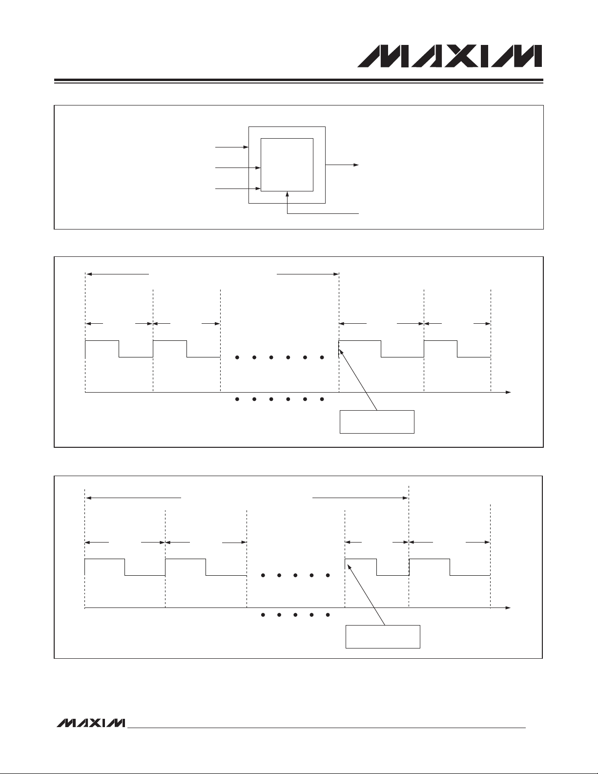
MAXQ Family User’s Guide:
MAXQ2010 Supplement
4096Hz
TSGN
TRIM[3:0]
Figure 14-2. RTC Prescaler and Trim
AVERAGE = [(1 - 73.2µs) x 9 + (1 + 732µs)]/10 = 1s
ADJUSTMENT
PRESCALER
TRIM
LOGIC
256Hz
10-SECOND CLOCK
1s - 73.2µs 1s - 73.2µs
1Hz
OUTPUT
TIME (t)
1 2 3
Figure 14-3. RTC Trim Adjustment (TSGN = 1)
AVERAGE = [(1s + 73.2µs) x 9 + (1 - 732µs)]/10 = 1s
1Hz
OUTPUT
1s + 73.2µs 1s + 73.2µs
1s + 732µs
10 11 12
ADJUSTMENT MADE HERE
(TSGN = 1)
1s - 732µs 1s + 73.2µs
1s - 73.2µs
SECONDS
1 2 3 10 11 12
ADJUSTMENT MADE HERE
(TSGN = 0)
Figure 14-4. RTC Trim Adjustment (TSGN = 0)
SECONDSTIME (t)
14-3
Page 66

MAXQ Family User’s Guide:
MAXQ2010 Supplement
14.4 RTC Register Descriptions
Addresses of registers are given as “Mx[yy],” where x is the module number (from 0 to 15 decimal) and yy is the register index (from 00h to 1Fh hexadecimal). Fields in the bit definition tables are defined as follows:
• Name: Symbolic names of bits or bit fields in this register.
• Reset: The value of each bit in this register following a standard reset. If this field reads “unchanged,” the given bit
is unaffected by standard reset. If this field reads “s,” the given bit does not have a fixed 0 or 1 reset value because
its value is determined by another internal state or external condition.
• POR: If present this field defines the value of each bit in this register following a power-on reset (as opposed to a
standard reset). Some bits are unaffected by standard resets and are set/cleared by POR only.
• Access: Bits can be read-only (r) or read/write (rw). Any special restrictions or conditions that could apply when
reading or writing this bit are detailed in the bit description.
14.4.1 RTC Trim Register (RTRM, M0[18h])
Bit #
Name TSGN — — — TRM
Reset 0 0 0 0 0 0 0 0
Access rw rw rw rw rw rw rw rw
7 6 5 4 3 2 1 0
Note 1: This register is reset by power-on reset only.
Note 2: Write to this register is ignored when WE = 0 or RCNT.BUSY = 1.
Bit 7: RTC Trim Sign Bit (TSGN). This register bit selects whether 32K clocks are inserted (TSGN = 1) or removed
(TSGN = 0).
Bits 6:4: Reserved. Read returns zero.
Bits 3:0: RTC Trim Calibration Register (TRM[3:0]). These register bits provide a binary value between 00h to 0Fh,
which is used for adjusting 32K clocks insertion/removal. At every 10-second interval, a number of 32K clocks equal to
the RTRM[3:0] numeric value x 8 is inserted/removed from the RTC counter depending on the TSGN sign bit.
14.4.2 RTC Control Register (RCNT, M0[19h])
Bit #
Name WE — ACS — — — FT SQE
Reset 0 1 0 0 0 0 0 0
Access rw rw rw rw rw rw rw rw
Bit #
Name ALSF ALDF RDYE RDY BUSY ASE ADE RTCE
Reset 0 0 0 0 0 0 0 0
Access rw rw rw rw r rw rw rw
Note 1: Bits 0 and 13 are reset by power-on reset only.
Note 2: Bits 14, 12:4, and 2:1 are reset by any reset source.
Note 3: Bit 3 is set to a 1 on system reset.
Note 4: Bit 0 is only writable when WE = 1 and BUSY = 0.
Note 5: Bit 13 is only writable when RTCE = 0.
Note 6: Bits 9:6 and 2:1 are only writable when BUSY = 0.
15 14 13 12 11 10 9 8
7 6 5 4 3 2 1 0
14-4
Page 67

MAXQ Family User’s Guide:
MAXQ2010 Supplement
Bit 15: RTC Write Enable (WE). This register bit serves as a protection mechanism against undesirable writes to the
RTCE bit and RTRM register. This bit must be set to a 1 to give write access to the RTRM register and the RTCE bit;
otherwise (when WE bit = 0) these protected bits are read-only.
Bit 14: Reserved. Read returns 1 after reset, or last written value (when BUSY = 0).
Bit 13: Alternate Clock Select (ACS). This bit enables the use of the system clock to drive the RTC in place of the
32kHz clock. When the alternate clock is selected (ACS = 1), the RTC input clock is driven by system clock/128. This
bit is provided for those applications where a 32kHz clock may not be present, or when the RTC module is intended
to be used as a timer based on the system clock. This bit can only be changed when RTCE = 0. When ACS = 1, the
RTC is effectively halted any time that the system clock is disabled (e.g., stop mode).
Bits 12:10: Reserved. Read returns zero.
Bit 9: RTC Frequency Test (FT). This register bit selects the frequency output on the SQW pin if the square-wave out-
put is enabled (SQE = 1). Setting FT = 1 selects the RTC input clock/8 output (512Hz for 32.768kHz applied to 32KIN),
while FT = 0 selects the RTC input clock/4096 (1Hz for 32.768kHz applied to 32KIN). This bit has no function when the
square-wave output is disabled (SQE = 0).
Bit 8: RTC Square-Wave Output Enable (SQE). Setting this bit to 1 enables the frequency specified by FT to be
outputted to the SQW pin. When cleared to 0, the SQW pin is not driven by the RTC.
Bit 7: Alarm Subsecond Flag (ALSF). This bit is set when the subsecond timer has been reloaded by the RSSA register. Setting the ALSF causes an interrupt request to the CPU if the ASE is set and interrupt is allowed at the system
level. This flag must be cleared by software once set. This alarm is qualified as wake-up to the stop and the switchback
function if its interrupt has not been masked.
Bit 6: Alarm Time-of-Day Flag (ALDF). This bit is set when the contents of RTSH and RTSL counter registers match
the 20-bit value in the RASH and RASL alarm registers. Setting the ALDF causes an interrupt request to the CPU if the
ADE is set and interrupt is allowed at the system level. This flag must be cleared by software once set. This alarm is
qualified as wake-up to the stop and the switchback function if its interrupt has not been masked.
Bit 5: RTC Ready Enable (RDYE). Setting this bit to 1 allows a system interrupt to be generated when RDY becomes
active (if interrupts are enabled globally and modularly). Clearing this bit to 0 disables the RDY interrupt.
Bit 4: RTC Ready (RDY). This bit is set to 1 by hardware when the RTC count registers update. It can be cleared to
0 by software at any time. It is also cleared to 0 by hardware just prior to an update of the RTC count register. This bit
can generate an interrupt if the RDYE bit is set to 1
Bit 3: RTC Busy (BUSY). This bit is set to 1 by hardware when any of the following conditions occur:
1) System reset.
2) Software writes to RTC count registers or trim register.
3) Software changes RTCE, ASE, or ADE.
For conditions 2 and 3, the write or change should not be considered complete until hardware clears the BUSY bit.
This is an indication that a 32kHz synchronized version of the register bit(s) is in place.
Bit 2: Alarm Subsecond Enable (ASE). The ASE bit is the RTC’s subsecond timer enable and must be set to logic 1
for the subsecond alarm to generate a system interrupt request. When the ASE is cleared to logic 0, the subsecond
alarm is disabled and no interrupt is generated, even if the alarm is set.
Bit 1: Alarm Time-of-Day Enable (ADE). The ADE bit is the RTC’s time-of-day alarm enable and must be set to logic
1 for the alarm to generate a system interrupt request. When the ADE is cleared to logic 0, the time-of-day alarm is
disabled and no interrupt is generated, even if the alarm is set.
Bit 0: RTC Enable (RTCE). Setting this bit to logic 1 activates the clocking by allowing the divided clock to the ripple
counters. Clearing this bit to logic 0 disables the clock.
14-5
Page 68

MAXQ Family User’s Guide:
MAXQ2010 Supplement
14.4.3 Real-Time Subsecond Counter Register (RTSS, M0[1Ah])
Bit #
Name RTSS
Reset 0 0 0 0 0 0 0 0
Access rw rw rw rw rw rw rw rw
Note 1: This register is cleared by power-on reset only.
Note 2: Read accessible when RDY = 1.
Note 3: Write accessible when RTCE = 0 and BUSY = 0.
Bits 7:0: RTC Subsecond Counter Register. This ripple counter represents 1/256-second resolution for the RTC and
its content is incremented with each 256Hz clock tick derived from the 32.768kHz oscillator. When the counter rolls
over, its output is used to drive the 32-bit second counter.
14.4.4 RTC Seconds Counter High Register (RTSH, M0[1Bh])
Bit #
Name RTSH
Reset 0 0 0 0 0 0 0 0
Access rw rw rw rw rw rw rw rw
7 6 5 4 3 2 1 0
15 14 13 12 11 10 9 8
Bit #
Name RTSH
Reset 0 0 0 0 0 0 0 0
Access rw rw rw rw rw rw rw rw
Note 1: This register is cleared by power-on reset only.
Note 2: Read accessible when RDY = 1.
Note 3: Write accessible when RTCE = 0 and BUSY = 0.
7 6 5 4 3 2 1 0
Bits 15:0: RTC Second Counter High Register. This register contains the most significant bits for the 32-bit second
counter. The RTC is a 48-bit ripple counter consisting of three cascaded counter registers: the 8-bit subsecond counter
(RTSS), the 16-bit low-order seconds counter (RTSL), and the 16-bit high-order second counter (RTSH).
14.4.5 RTC Seconds Counter Low Register (RTSL, M0[1Ch])
Bit #
Name RTSL
Reset 0 0 0 0 0 0 0 0
Access rw rw rw rw rw rw rw rw
Bit #
Name RTSL
Reset 0 0 0 0 0 0 0 0
Access rw rw rw rw rw rw rw rw
15 14 13 12 11 10 9 8
7 6 5 4 3 2 1 0
Note 1: This register is cleared by power-on reset only.
Note 2: Read accessible when RDY = 1.
Note 3: Write accessible when RTCE = 0 and BUSY = 0.
Bits 15:0: RTC Second Counter Low Register. This register contains the least significant bits for the 32-bit second
counter. The RTC is a 48-bit ripple counter consisting of three cascaded counter registers: the 8-bit subsecond counter
(RTSS), the 16-bit low-order seconds counter (RTSL), and the 16-bit high-order second counter (RTSH).
14-6
Page 69

MAXQ Family User’s Guide:
MAXQ2010 Supplement
14.4.6 RTC Subsecond Alarm Register (RSSA, M0[1Dh])
Bit #
Name RSSA
Reset 0 0 0 0 0 0 0 0
Access rw rw rw rw rw rw rw rw
Note: Write accessible when BUSY = 0 and either ASE = 0 or RTCE = 0.
7 6 5 4 3 2 1 0
Bits 7:0: RTC Subsecond Alarm Register. This register contains the reload value for the subsecond alarm. The ALSF
bit is set when an autoreload occurs.
14.4.7 RTC Time-of-Day Alarm High Register (RASH, M0[1Eh])
Bit #
Name RASH
Reset 0 0 0 0 0 0 0 0
Access rw rw rw rw rw rw rw Rw
Note: Write accessible when BUSY = 0 and either ASE = 0 or RTCE = 0.
Bits 7:0: RTC Time-of-Day Alarm High Register. This register contains the most significant bits for the 24-bit time-ofday alarm. The time-of-day alarm is formed by the RASH and the RASL registers, and only the lower 20 bits is meaningful for the alarm function. Each time the subsecond counter rolls over (once per second), the RTC compares the lowest
20 bits of the time-of-day alarm setting (RASH[3:0]:RASL[15:0]) with the 20 least significant bits of the seconds counter
(RTSH[3:0]:RTSL[15:0]). The time-of-day alarm is triggered when these two 20-bit values match.
7 6 5 4 3 2 1 0
14.4.8 RTC Time-of-Day Alarm Low Register (RASL, M0[1Fh])
Bit #
Name RASL
Reset 0 0 0 0 0 0 0 0
Access rw rw rw rw rw rw rw rw
Bit #
Name RASL
Reset 0 0 0 0 0 0 0 0
Access rw rw rw rw rw rw rw rw
Note: Write accessible when BUSY = 0 and either ASE = 0 or RTCE = 0.
Bits 15:0: RTC Time-of-Day Alarm Low Register. This register contains the least significant bits for the 20-bit time-ofday alarm. The time-of-day alarm is formed by the RASH and the RASL registers and only the lower 20 bits are meaningful for the alarm function. Each time the subsecond counter rolls over (once per second), the RTC compares the
lowest 20 bits of the time-of-day alarm setting (RASH[3:0]:RASL[15:0]) with the 20 least significant bits of the seconds
counter (RTSH[3:0]:RTSL[15:0]). The time-of-day alarm is triggered when these two 20-bit values match.
15 14 13 12 11 10 9 8
7 6 5 4 3 2 1 0
14-7
Page 70

MAXQ Family User’s Guide:
MAXQ2010 Supplement
14.5 RTC Example: Starting and Setting the Clock
move RCNT, #08000h ;RTC write enable
call wait_busy ;Call subroutine to verify RCNT.3 (BUSY) is low
move RTSS, #00h ;Clear sub-second count
move RTSL, #0000h ;Clear low-order seconds counter
move RTSH, #0000h ;Clear high-order seconds counter
move RCNT, #08001h ;Start clock
14-8
Page 71

MAXQ Family User’s Guide:
MAXQ2010 Supplement
ADDENDUM TO SECTION 15: TEST ACCESS PORT (TAP)
The JTAG/TAP port on the MAXQ2010 is multiplexed with port pins P6.0, P6.1, P6.2, and P6.3. These pins default to the
JTAG/TAP function on reset, which means that the part is always ready for in-circuit debugging or in-circuit programming operations following any reset.
Once an application has been loaded and starts running, the JTAG/TAP port can still be used for in-circuit debugging
operations. If in-circuit debugging functionality is not needed, the associated port pins can be reclaimed for application use by setting the TAP (SC.7) bit to 0. This disables the JTAG/TAP interface and allows the four pins to operate
as normal port pins.
15-1
Page 72

MAXQ Family User’s Guide:
MAXQ2010 Supplement
ADDENDUM TO SECTION 16: IN-CIRCUIT DEBUG MODE
The MAXQ2010 provides an in-circuit debugging interface through the debug port as described in the MAXQ Family
User’s Guide. This interface provides the following functions for use in debugging application software:
• Single-step (trace) execution
• Four program address breakpoints
• Two breakpoints configurable as data address or register address breakpoints
• Register read and write
• Program stack read
• Data memory read and write
• Optional password protection
The following sections provide specific notes on the operation of the MAXQ2010 in debugging mode.
16.1 Register Read and Write Commands
Any register location can be read or written using these commands, including reserved locations and those used for
op code support. No protection is provided by the debugging interface, and avoiding side effects is the responsibility
of the host system communicating with the MAXQ2010.
Writing to the IP register alters the address that execution resumes at once the debugging engine exits.
In general, reading a register through the debug interface returns the value that was in that register before the debugging engine was invoked. An exception to this rule is the SP register; reading the SP register through the debug interface actually returns the value (SP+1).
16.2 Data Memory Read Command
When invoking this command, ICDA should be set to the word address of the starting location to read from, and ICDD
should be set to the number of words. The input address must be based on the utility ROM memory map, as shown
in Figure 2-3.
Data memory words returned by this command are output LSB first.
16.3 Data Memory Write Command
When invoking this command, ICDA should be set to the word address of the location to write to, and ICDD should be
set to the data word to write. The input address must be based on the utility ROM memory map, as shown in Figure 2-3.
16.4 Program Stack Read Command
When invoking this command, ICDA should be set to the address of the starting stack location (value of SP) to read
from, and ICDD should be set to the number of words. The address given in ICDA is the highest value that is used, as
words are popped off the stack and returned in descending order.
Stack words returned by this command are output LSB first.
16.5 Read Register Map Command
This command outputs all peripheral registers in the range M0[00h] to M4[0Fh], along with a fixed set of system registers. The following formatting rules apply to the returned data:
• System registers are output as 8 bits or 16 bits, least significant byte first.
• All peripheral registers are output as 16 bits, least significant byte first. The top byte of 8-bit registers are returned
as 00h.
• Nonimplemented and reserved peripheral registers in the range M0[00h] to M4[0Fh] are represented as empty word
values in Table 16-1. These values should be ignored.
16-1
Page 73

MAXQ Family User’s Guide:
MAXQ2010 Supplement
• Registers SPIB, I2CBUF, and ADDATA are not read, and their values are returned as 0000h.
The first byte output by this command is the value 144 (090h), which represents the number of peripheral register
words output. Table 16-1 lists the remaining 352 bytes output by this command.
Table 16-1. Output from DebugReadMap Command
x0 x1 x2 x3 x4 x5 x6 x7 x8 x9 xA xB xC xD xE xF
0x
1x
2x
3x
4x
5x
6x
7x
8x
9x
Ax
Bx
Cx
Dx
Ex
Fx
10x
11x
12x
13x
14x
15x
PO0 PO1 PO2 PO3 EIF0 EIE0 — —
PI0 PI1 PI2 PI3 EIES0 — — PWCN
PD0 PD1 PD2 PD3 — — — —
RTRM RCNT RTSS RTSH RTSL RSSA RASH RASL
PO4 PO5 PO6 0000h EIF1 EIE1 EIF2 EIE2
PI4 PI5 PI6 EIES1 EIES2 SVM — —
PD4 PD5 PD6 — — SPICN SPICF SPICK
— — — — — — — —
MCNT MA MB MC2 MC1 MC0 LCFG —
MC1R MC0R LCRA LCD0 LCD1 LCD2 LCD3 LCD4
LCD5 LCD6 LCD7 LCD8 LCD9 LCD10 LCD11 LCD12
LCD13 LCD14 LCD15 LCD16 LCD17 LCD18 LCD19 LCD20
0000h I2CST I2CIE — SCON0 SBUF0 SCON1 SBUF1
SMD0 PR0 SMD1 PR1 I2CCN I2CCK I2CTO I2CSLA
— — — — — — — —
— — — — — — — —
TB0R TB0C TB1R TB1C TB2R TB2C ADST ADADDR
TB0CN TB0V TB1CN TB1V TB2CN TB2V ADCN 0000h
AP APC PSF IC IMR SC IIR CKCN WDCN 00 A[0] A[1] A[2]
A[3] A[4] A[5] A[6] A[7] A[8] A[9] A[10]
A[11] A[12] A[13] A[14] A[15] IP SP+1 IV
LC[0] LC[1] OFFS DPC GR BP DP[0] DP[1]
16-2
Page 74

MAXQ Family User’s Guide:
MAXQ2010 Supplement
ADDENDUM TO SECTION 17: IN-SYSTEM PROGRAMMING (JTAG)
The MAXQ2010 provides a JTAG-compatible debug port interface for in-system programming (bootloader) operations.
In order to use this interface for in-system programming, the SPE bit must be set through the debug port. This is done
while the device is held in reset, using the system programming instruction as described in the MAXQ Family User’s
Guide.
17.1 JTAG Bootloader Protocol
The only bootloader interface supported for the MAXQ2010 is the debug port. When using the debug port, the clock
rate (TCK) must be kept below 1/8 the system clock rate.
All bootloader commands begin with a single command byte. The high four bits of this command byte define the command family (from 0 to 15), while the low four bits define the specific command within that family.
All commands (except for those in Family 0) follow this format:
BYTE 1 BYTE 2 BYTE 3 BYTE 4 (LENGTH) BYTES/WORDS
Command Length Param 1 Param 2 Data
After each command has completed, the loader outputs a “prompt” byte to indicate that it has finished the operation.
The prompt byte is the single character “>” (byte value 03Eh).
Bootloader commands that fail for any reason set the bootloader status byte to an error code value describing the
reason for the failure. This status byte can be read by means of the Get Status command (04h).
Table 17-1. Bootloader Status Codes
STATUS
VALUE
00 No Error. The last command completed successfully.
01 Family Not Supported. An attempt was made to use a command from a family the bootloader does not support.
02 Invalid Command. An attempt was made to use a nonexistent command within a supported command family.
03
04 Bad Parameter. The parameter (address or otherwise) passed to the command was out of range or otherwise invalid.
05 Verify Failed. The verification step failed on a Load/Verify or Verify command.
06 Unknown Register. An attempt was made to read from or write to a nonexistent register.
07
08 Master Erase Failed. The bootloader was unable to perform master erase.
All commands in Family 0 can be executed without first matching the password. All other commands (in families 1x
through Fx) are password protected; the password must first be matched before these commands can be executed.
A special case exists when the program memory has not been initialized (following master erase). If the password
(stored in word locations 0010h to 001Fh in program memory) is all 0000h words or all FFFFh words, the bootloader
treats the password as having been matched and automatically unlocks the password bit. This allows access to
password-protected commands following master erase (when no password has been set in program memory).
When providing addresses for code or data read or write to bootloader commands, all addresses run from 0000h to
(memory size – 1).
No Password Match. An attempt was made to use a password-protected command without first matching a valid
password. Or, the Match Password command was called with an incorrect password value.
Word Mode Not Supported. An attempt was made to set word-mode access, but the bootloader supports byte-mode
access only.
FUNCTION
17-1
Page 75

MAXQ Family User’s Guide:
MAXQ2010 Supplement
17.2 Family 0 Commands (Not Password Protected)
Command 00h—No Operation
I/O BYTE 1
Input
Output
Command 01h—Exit Loader
This command causes the bootloader command loop to exit. Upon exit, the MAXQ2010 clears the SPE bit and resets
itself internally. Following the internal reset, execution jumps to the beginning of application code at address 0000h.
I/O BYTE 1
Input
Output
Command 02h—Master Erase
This command erases (programs to FFFFh) all words in the program flash memory and writes all words in the data
SRAM to zero. After this command completes, the password lock bit is automatically cleared, allowing access to all
bootloader commands.
00h
01h
I/O BYTE 1
Input
Output
02h
Command 03h—Password Match
This command accepts a 32-byte password value, which is matched against the password in program memory (in byte
mode) from addresses 0020h to 003Fh. If the value matches, the password lock is cleared.
I/O BYTE 1 BYTES 2 TO 33 BYTE 34 BYTE 35
Input
Output
03h 32-Byte Password Value 00h 00h
03Eh
Command 04h—Get Status
The status code returned by this command is defined in Table 17-1. The flags byte contains the bit status flags as
shown in Table 17-2.
I/O BYTE 1 BYTE 2 BYTE 3 BYTE 4 BYTE 5
Input
Output
04h 00h 00h 00h 00h
Flags Status Code 03Eh
17-2
Page 76

MAXQ Family User’s Guide:
MAXQ2010 Supplement
Table 17-2. Bootloader Status Flags
FLAG BIT FUNCTION
Password Lock
0
1
2
3 to 8 Reserved
Command 05h—Get Supported Commands
The SupportL (LSB) and SupportH (MSB) bytes form a 16-bit value that indicates which command families this bootloader supports. If bit 0 is set to 1, it indicates that Family 0 is supported. If bit 1 is set to 1, it indicates that Family 1
is supported, and so on. For the MAXQ2010, the value returned is 403Fh, indicating that command families 0, 1, 2, 3,
4, 5 and E are supported.
The CodeLen and DataLen bytes return the fixed block lengths used by the Load/Dump/Verify Fixed Length commands
for code and data space, respectively. Because fixed block load is not supported on the MAXQ2010, both these values
are returned as 00h.
0 = The password is unlocked or had a default value; password-protected commands can be used.
1 = The password is locked. Password-protected commands cannot be used.
Word/Byte Mode
0 = The bootloader is currently in byte mode for memory reads/writes.
1 = The bootloader is currently in word mode for memory reads/writes. (Note: The MAXQ2010 supports byte mode
only.)
Word/Byte Mode Supported
0 = The bootloader supports byte mode only.
1 = The bootloader supports word mode as well as byte mode. (Note: The MAXQ2010 supports byte mode only.)
I/O BYTE 1 BYTE 2 BYTE 3 BYTE 4 BYTE 5 BYTE 6 BYTE 7
Input
Output
05h 00h 00h 00h 00h 00h 00h
SupportL SupportH CodeLen DataLen 03Eh
Command 06h—Get Code Size
This command returns SizeH:SizeL, which represents the size of available code memory in words minus 1. If this command is unsupported, the return value is 0000h, meaning “unknown amount of memory”.
I/O BYTE 1 BYTE 2 BYTE 3 BYTE 4 BYTE 5
Input
Output
06h 00h 00h 00h 00h
SizeL SizeH 03Eh
Command 07h—Get Data Size
This command returns SizeH:SizeL, which represents the size of available data memory in words minus 1. If this command is unsupported, the return value is 0000h, meaning “unknown amount of memory”.
I/O BYTE 1 BYTE 2 BYTE 3 BYTE 4 BYTE 5
Input
Output
07h 00h 00h 00h 00h
SizeL SizeH 03Eh
17-3
Page 77

MAXQ Family User’s Guide:
MAXQ2010 Supplement
Command 08h—Get Loader Version
I/O BYTE 1 BYTE 2 BYTE 3 BYTE 4 BYTE 5
Input
Output
Command 09h—Get Utility ROM Version
I/O BYTE 1 BYTE 2 BYTE 3 BYTE 4 BYTE 5
Input
Output
Command 0Ah—Set Word/Byte-Mode Access
The mode byte should be 0 to set byte-access mode or 1 to set word-access mode. The current access mode is
returned in the status flag byte by command 04h, as well as a flag to indicate whether word-access mode is supported
by this particular bootloader. Note: The MAXQ2010 supports byte mode only.
I/O BYTE 1 BYTE 2 BYTE 3 BYTE 4
Input
Output
08h 00h 00h 00h 00h
VersionL VersionH 03Eh
09h 00h 00h 00h 00h
VersionL VersionH 03Eh
0Ah Mode 00h 00h
03Eh
Command 0Dh—Get ID Information
For the MAXQ2010, the information returned by this command is a zero-terminated ROM banner string.
I/O BYTE 1 (VARIABLE) LAST BYTE
Input
Output
0Dh 00h, 00h, 00h . . . 00h
Device-Dependent Information 03Eh
17.3 Family 1 Commands: Load Variable Length (Password Protected)
Command 10h—Load Code Variable Length
This command programs (Length) bytes of data into the program flash starting at byte address (AddressH:AddressL),
with the following restrictions.
• The low bit of the address is always forced to zero, since instructions in program flash must be word aligned.
• In byte mode, if an odd number of bytes is input, the final word written to the program flash has its most significant
byte set to 00h by default.
• Memory locations in flash that have previously been loaded must be erased (using the Master Erase command, the
Erase Code Fixed Length command, or the flashErasePage or flashEraseAll utility ROM routines) before they can
be loaded with a different value.
• In keeping with standard MAXQ little-endian memory architecture, the least significant byte of each word is loaded
first. For example, if one loads bytes (11h, 22h, 33h, 44h) starting at address 0000h, the first two words of program
space are written to (2211h, 4433h).
I/O BYTE 1 BYTE 2 BYTE 3 BYTE 4
Input
Output
10h Length AddressL AddressH Data to load 00h 00h
(LENGTH)
BYTES
BYTE
LENGTH+5
BYTE
LENGTH+6
03Eh
17-4
Page 78

MAXQ Family User’s Guide:
MAXQ2010 Supplement
Command 11h—Load Data Variable Length
This command writes (Length) bytes of data into the data SRAM starting at byte address (AddressH:AddressL).
I/O BYTE 1 BYTE 2 BYTE 3 BYTE 4
Input
Output
11h Length AddressL AddressH Data to load 00h 00h
(LENGTH)
BYTES
BYTE
LENGTH+5
BYTE
LENGTH+6
03Eh
17.4 Family 2 Commands: Dump Variable Length (Password Protected)
Command 20h—Dump Code Variable Length
This command has a slightly different format depending on the length of the dump requested. It returns the contents
of the program flash memory: (Length) or (LengthH:LengthL) bytes starting at byte address (AddrH:AddrL).
I/O BYTE 1 BYTE 2 BYTE 3 BYTE 4 BYTE 5 BYTE 6
Input (to
dump
< 256 bytes)
Output
I/O BYTE 1 BYTE 2 BYTE 3 BYTE 4 BYTE 5 BYTE 6 BYTE 7
Input (to
dump
256+ bytes)
Output
20h 1 AddrL AddrH Length 00h 00h... 00h
20h 2 AddrL AddrH LengthL LengthH 00h 00h... 00h
(LENGTH)
BYTES
Memory
contents
(LENGTH)
BYTES
Memory
contents
BYTE
LENGTH+7
03Eh
BYTE
LENGTH+8
03Eh
Command 21h—Dump Data Variable Length
This command has a slightly different format depending on the length of the dump requested. It returns the contents
of the data SRAM - (Length) or (LengthH:LengthL) bytes starting at byte address (AddrH:AddrL).
I/O BYTE 1 BYTE 2 BYTE 3 BYTE 4 BYTE 5 BYTE 6
Input (to
dump
< 256 bytes)
Output
I/O BYTE 1 BYTE 2 BYTE 3 BYTE 4 BYTE 5 BYTE 6 BYTE 7
Input (to
dump
256+ bytes)
Output
21h 1 AddrL AddrH Length 00h 00h... 00h
21h 2 AddrL AddrH LengthL LengthH 00h 00h... 00h
(LENGTH)
BYTES
Memory
contents
(LENGTH)
BYTES
Memory
contents
BYTE
LENGTH+7
03Eh
BYTE
LENGTH+8
03Eh
17-5
Page 79

MAXQ Family User’s Guide:
MAXQ2010 Supplement
17.5 Family 3 Commands: CRC Variable Length (Password Protected)
Command 30h—CRC Code Variable Length
This command has a slightly different format depending on the length of the CRC requested. It returns the CRC-16
value (CrcH:CrcL) of the program flash - (Length) or (LengthH:LengthL) bytes/words starting at (AddrH:AddrL).
I/O BYTE 1 BYTE 2 BYTE 3 BYTE 4 BYTE 5 BYTE 6 BYTE 7 BYTE 8 BYTE 9
Input (to CRC
< 256 bytes)
Output
I/O BYTE 1 BYTE 2 BYTE 3 BYTE 4 BYTE 5 BYTE 6 BYTE 7 BYTE 8 BYTE 9 BYTE 10
Input (to CRC
256+ bytes)
Output
Command 31h—CRC Data Variable Length
This command has a slightly different format depending on the length of the CRC requested. It returns the CRC-16
value (CrcH:CrcL) of the data SRAM - (Length) or (LengthH:LengthL) bytes/words starting at (AddrH:AddrL).
I/O BYTE 1 BYTE 2 BYTE 3 BYTE 4 BYTE 5 BYTE 6 BYTE 7 BYTE 8 BYTE 9
Input (to CRC
< 256 bytes)
Output
30h 1 AddrL AddrH Length 00h 00h 00h 00h
CrcH CrcL 03Eh
30h 2 AddrL AddrH LengthL LengthH 00h 00h 00h 00h
CrcH CrcL 03Eh
31h 1 AddrL AddrH Length 00h 00h 00h 00h
CrcH CrcL 03Eh
I/O BYTE 1 BYTE 2 BYTE 3 BYTE 4 BYTE 5 BYTE 6 BYTE 7 BYTE 8 BYTE 9 BYTE 10
Input (to CRC
256+ bytes)
Output
31h 2 AddrL AddrH LengthL LengthH 00h 00h 00h 00h
CrcH CrcL 03Eh
17.6 Family 4 Commands: Verify Variable Length (Password Protected)
Command 40h—Verify Code Variable Length
This command operates in the same manner as the “Load Code Variable Length” command, except that instead of
programming the input data into flash memory, it verifies that the input data matches the data already in code space.
If the data does not match, the status code is set to reflect this failure.
I/O BYTE 1 BYTE 2 BYTE 3 BYTE 4
Input
Output
40h Length AddressL AddressH Data to verify 00h 00h
(LENGTH)
BYTES
Command 41h—Verify Data Variable Length
This command operates in the same manner as the “Load Data Variable Length” command, except that instead of
writing the input data into data SRAM, it verifies that the input data matches the data already in data space. If the data
does not match, the status code is set to reflect this failure.
I/O BYTE 1 BYTE 2 BYTE 3 BYTE 4
Input
Output
41h Length AddressL AddressH Data to verify 00h 00h
(LENGTH)
BYTES
BYTE
LENGTH+5
BYTE
LENGTH+5
BYTE
LENGTH+6
03Eh
BYTE
LENGTH+6
03Eh
17-6
Page 80

MAXQ Family User’s Guide:
MAXQ2010 Supplement
17.7 Family 5 Commands: Load and Verify Variable Length (Password Protected)
Command 50h—Load and Verify Code Variable Length
This command combines the functionality of the “Load Code Variable Length” and “Verify Code Variable Length”
commands.
I/O BYTE 1 BYTE 2 BYTE 3 BYTE 4
Input
Output
50h Length AddressL AddressH
(LENGTH)
BYTES
Data to load
and verify
BYTE
LENGTH+5
00h 00h
BYTE
LENGTH+6
03Eh
Command 51h—Load and Verify Data Variable Length
This command combines the functionality of the “Load Data Variable Length” and “Verify Data Variable Length”
commands.
I/O BYTE 1 BYTE 2 BYTE 3 BYTE 4
Input
Output
51h Length AddressL AddressH
(LENGTH)
BYTES
Data to load
and verify
BYTE
LENGTH+5
00h 00h
BYTE
LENGTH+6
03Eh
17.8 Family E Commands: Erase Fixed Length (Password Protected)
Command E0h—Erase Code Fixed Length
This command erases (programs to FFFFh) all words in a 512-word page of the program flash memory. The address
given should be located in the 512-word page to be erased. For example, providing address 0000h (in byte mode) to
this command erases the first 512-word page, address 0400h erases the second page, and so on. There are 64 flash
pages total, from 0000h to 7C00h.
I/O BYTE 1 BYTE 2 BYTE 3 BYTE 4
Input
Output
E0h 0 AddressL AddressH
17-7
Page 81

MAXQ Family User’s Guide:
MAXQ2010 Supplement
ADDENDUM TO SECTION 18: MAXQ FAMILY INSTRUCTION SET SUMMARY
Refer to the MAXQ Family User’s Guide. Table 18-1 from the MAXQ Family User’s Guide is reproduced here.
Table 18-1. Instruction Set Summary
MNEMONIC DESCRIPTION
AND src
OR src
XOR src
CPL
NEG
SLA Shift Acc left arithmetically 1000 1010 0010 1010 C, S, Z Y
SLA2 Shift Acc left arithmetically twice 1000 1010 0011 1010 C, S, Z Y
SLA4 Shift Acc left arithmetically four times 1000 1010 0110 1010 C, S, Z Y
RL Rotate Acc left (w/o C) 1000 1010 0100 1010 S Y
RLC Rotate Acc left (through C) 1000 1010 0101 1010 C, S, Z Y
SRA Shift Acc right arithmetically 1000 1010 1111 1010 C, Z Y
SRA2 Shift Acc right arithmetically twice 1000 1010 1110 1010 C, Z Y
LOGICAL OPERATIONS
SRA4 Shift Acc right arithmetically four times 1000 1010 1011 1010 C, Z Y
SR
RR Rotate Acc right (w/o C) 1000 1010 1100 1010 S Y
RRC Rotate Acc right (though C) 1000 1010 1101 1010 C, S, Z Y
MOVE C, Acc.<b>
MOVE C, #0
MOVE C, #1
CPL C
MOVE Acc.<b>, C
AND Acc.<b>
OR Acc.<b>
XOR Acc.<b>
BIT OPERATIONS
MOVE dst.<b>, #1
MOVE dst.<b>, #0
MOVE C, src.<b>
ADD src
ADDC src
SUB src
MATH
SUBB src
Acc ← Acc AND src
Acc ← Acc OR src
Acc ← Acc XOR src
Acc ← ~Acc
Acc ← ~Acc + 1
Shift Acc right (0 → msbit)
C ← Acc.<b>
C ← 0
C ← 1
C ← ~C
Acc.<b> ← C
C ← C AND Acc.<b>
C ← C OR Acc.<b>
C ← C XOR Acc.<b>
dst.<b> ← 1
dst.<b> ← 0
C ← src.<b>
Acc ← Acc + src
Acc ← Acc + (src + C)
Acc ← Acc – src
Acc ← Acc – (src + C)
16-BIT INSTRUCTION
WORD
f001 1010 ssss ssss S, Z Y 1
f010 1010 ssss ssss S, Z Y 1
f011 1010 ssss ssss S, Z Y 1
1000 1010 0001 1010 S, Z Y
1000 1010 1001 1010 S, Z Y
1000 1010 1010 1010 C, S, Z Y
1110 1010 bbbb 1010 C
1101 1010 0000 1010 C
1101 1010 0001 1010 C
1101 1010 0010 1010 C
1111 1010 bbbb 1010 S, Z
1001 1010 bbbb 1010 C
1010 1010 bbbb 1010 C
1011 1010 bbbb 1010 C
1ddd dddd 1bbb 0111 C, S, E, Z 2
1ddd dddd 0bbb 0111 C, S, E, Z 2
fbbb 0111 ssss ssss C
f100 1010 ssss ssss C, S, Z, OV Y 1
f110 1010 ssss ssss C, S, Z, OV Y 1
f101 1010 ssss ssss C, S, Z, OV Y 1
f111 1010 ssss ssss C, S, Z, OV Y 1
STATUS
BITS
AFFECTED
AP
INC/DEC
NOTES
18-1
Page 82

Table 18-1. Instruction Set Summary (continued)
MAXQ Family User’s Guide:
MAXQ2010 Supplement
MNEMONIC DESCRIPTION
{L/S}JUMP src
{L/S}JUMP C, src
{L/S}JUMP NC, src
{L/S}JUMP Z, src
{L/S}JUMP NZ, src
{L/S}JUMP E, src
{L/S}JUMP NE, src
{L/S}JUMP S, src
{L/S}DJNZ LC[n], src
{L/S}CALL src
RET
RET C
RET NC
BRANCHING
RET Z
RET NZ
RET S
RETI
RETI C
RETI NC
RETI Z
RETI NZ
RETI S
XCH (MAXQ20 only) Swap Acc bytes 1000 1010 1000 1010 S Y
XCHN Swap nibbles in each Acc byte 1000 1010 0111 1010 S Y
MOVE dst, src
PUSH src
DATA
POP dst
TRANSFER
POPI dst
CMP src
NOP No operation 1101 1010 0011 1010
Note 1: The active accumulator (Acc) is not allowed as the src in operations where it is the implicit destination.
Note 2: Only module 8 and modules 0 to 5 (when implemented for a given product) are supported by these single-cycle bit opera-
tions. Potentially affects C or E if PSF register is the destination. Potentially affects S and/or Z if AP or APC is the destination.
Note 3: The terms Acc and A[AP] can be used interchangeably to denote the active accumulator.
Note 4: Any index represented by <b> or found inside [ ] brackets is considered variable, but required.
Note 5: The active accumulator (Acc) is not allowed as the dst if A[AP] is specified as the src.
Note 6: The ‘{L/S}’ prefix is optional.
Note 7: Instructions that attempt to simultaneously push/pop the stack (e.g. PUSH @SP--, PUSH @SPI--, POP @++SP, POPI
@++SP) or modify SP in a conflicting manner (e.g., MOVE SP, @SP--) are invalid.
Note 8: Special cases: If ‘MOVE APC, Acc’ sets the APC.CLR bit, AP is cleared, overriding any autoinc/dec/modulo operation
specified for AP. If ‘MOVE AP, Acc’ causes an autoinc/dec/modulo operation on AP, this overrides the specified data
transfer (i.e., Acc is not transferred to AP).
IP ← IP + src or src
If C=1, IP ← (IP + src) or src
If C=0, IP ← (IP + src) or src
If Z=1, IP ← (IP + src) or src
If Z=0, IP ← (IP + src) or src
If E=1, IP ← (IP + src) or src
If E=0, IP ← (IP + src) or src
If S=1, IP ← (IP + src) or src
If --LC[n] <> 0, IP← (IP + src) or src
@++SP ← IP+1; IP ← (IP+src) or src
IP ← @SP-If C=1, IP ← @SP-If C=0, IP ← @SP-If Z=1, IP ← @SP-If Z=0, IP ← @SP-If S=1, IP ← @SP-IP ← @SP-- ; INS← 0
If C=1, IP ← @SP-- ; INS← 0
If C=0, IP ← @SP-- ; INS← 0
If Z=1, IP ← @SP-- ; INS← 0
If Z=0, IP ← @SP-- ; INS← 0
If S=1, IP ← @SP-- ; INS← 0
dst ← src
@++SP ← src
dst ← @SP-dst ← @SP-- ; INS ← 0
E ← (Acc = src)
16-BIT INSTRUCTION
WORD
f000 1100 ssss ssss 6
f010 1100 ssss ssss 6
f110 1100 ssss ssss 6
f001 1100 ssss ssss 6
f101 1100 ssss ssss 6
0011 1100 ssss ssss 6
0111 1100 ssss ssss 6
f100 1100 ssss ssss 6
f10n 1101 ssss ssss 6
f011 1101 ssss ssss 6, 7
1000 1100 0000 1101
1010 1100 0000 1101
1110 1100 0000 1101
1001 1100 0000 1101
1101 1100 0000 1101
1100 1100 0000 1101
1000 1100 1000 1101
1010 1100 1000 1101
1110 1100 1000 1101
1001 1100 1000 1101
1101 1100 1000 1101
1100 1100 1000 1101
fddd dddd ssss ssss C, S, Z, E (Note 8) 7, 8
f000 1101 ssss ssss 7
1ddd dddd 0000 1101 C, S, Z, E 7
1ddd dddd 1000 1101 C, S, Z, E 7
f111 1000 ssss ssss E
STATUS
BITS
AFFECTED
AP
INC/DEC
NOTES
18-2
Page 83

MAXQ Family User’s Guide:
MAXQ2010 Supplement
SECTION 19: ANALOG-TO-DIGITAL CONVERTER (SPECIFIC TO MAXQ2010)
The MAXQ2010 provides a 12-bit, successive approximation analog-to-digital converter (ADC) with an integrated
analog multiplexer. The ADC can perform either single-ended conversions from one of eight channels or differential
conversions from one of four channel pairs. The voltage reference used for each conversion can be selected from an
internal precision bandgap reference, an external reference, or the AVDD analog power supply.
19.1 Analog-to-Digital Converter Features
• 12-bit single-ended conversion with up to eight analog channel inputs
• 12-bit differential conversion with up to four analog channel pair inputs (each differential pair takes the place of two
single-ended channel inputs)
• Autoscan feature performs up to eight conversions in sequence automatically without CPU intervention
• Conversion sequence can be performed once (single conversion mode) or repeatedly (continuous conversion mode)
• Up to 16 sample words can be stored in a dedicated data buffer until the processor is ready to retrieve them
• Selectable clock divider runs the ADC from a divide by 1, divide by 2, divide by 4, or divide by 8 of the system clock
• Sample acquisition time can optionally be extended on a per-conversion basis
• Data results can be left-aligned or right-aligned on a per-conversion basis
• Converter reference is switchable among AVDD, internal reference, and external reference
• Optional power management mode shuts the ADC off between conversions to save power
• Configurable data available interrupt signals the CPU following each conversion, each sequence, or after every 12
or 16 samples
CPU
INTERFACE
ADCN
ADST
ADADDR
ADDATA
Figure 19-1. ADC Block Diagram
ADCFG[0]
ADCFG[1]
ADCFG[2]
ADCFG[3]
ADBUF[0] ADBUF[8]
ADBUF[1] ADBUF[9]
ADBUF[2] ADBUF[10]
ADBUF[3] ADBUF[11]
ADBUF[4] ADBUF[12]
ADBUF[5] ADBUF[13]
ADBUF[6] ADBUF[14]
ADBUF[7] ADBUF[15]
ADCFG[4]
ADCFG[5]
ADCFG[6]
ADCFG[7]
12-BIT
SAR ADC
ADC
SEQUENCER
ANALOG
MULTIPLEXER
AN0
AN1
AN2
AN3
AN4
AN5
AN6
AN7
19-1
Page 84

MAXQ Family User’s Guide:
MAXQ2010 Supplement
19.2 Analog-to-Digital Pins and Control Registers
Tables 19-1 and 19-2 list the pins and control registers dedicated to the ADC. Note that all ADC pins are dedicated,
so none of them is multiplexed with GPIO port pins. Addresses for all registers are given as “Mx[yy],” where x is the
module number (from 0 to 15 decimal) and yy is the register index (from 00h to 1Fh hexadecimal). Fields in the bit
definition tables are defined as follows:
• Name: Symbolic names of bits or bit fields in this register.
• Reset: The value of each bit in this register following a standard reset. If this field reads “unchanged,” the given bit
is unaffected by standard reset. If this field reads “s,” the given bit does not have a fixed 0 or 1 reset value because
its value is determined by another internal state or external condition.
• POR: If present this field defines the value of each bit in this register following a power-on reset (as opposed to a
standard reset). Some bits are unaffected by standard resets and are set/cleared by POR only.
• Access: Bits can be read-only (r) or read/write (rw). Any special restrictions or conditions that could apply when
reading or writing this bit are detailed in the bit description.
Table 19-1. ADC Input and Power-Supply Pins
PIN NAME ADC INTERFACE FUNCTION
82 AVDD Analog Supply Voltage
79 AGND Analog Ground
70 AVREF External ADC Voltage Reference
78 AN0 Single-Ended Analog Input Channel 0
77 AN1 Single-Ended Analog Input Channel 1
76 AN2 Single-Ended Analog Input Channel 2
75 AN3 Single-Ended Analog Input Channel 3
74 AN4 Single-Ended Analog Input Channel 4
73 AN5 Single-Ended Analog Input Channel 5
72 AN6 Single-Ended Analog Input Channel 6
71 AN7 Single-Ended Analog Input Channel 7
78, 77 (AN0, AN1) Differential Input Channel 0
76, 75 (AN2, AN3) Differential Input Channel 1
74, 73 (AN4, AN5) Differential Input Channel 2
72, 71 (AN6, AN7) Differential Input Channel 3
Table 19-2. ADC Control Registers
REGISTER ADDRESS FUNCTION
ADST M4[06h]
ADADDR M4[07h]
ADCN M4[0Eh]
ADDATA M4[0Fh]
ADCFG[0] ADDATA[10h] ADC Sequence Configuration Register 0
ADCFG[1] ADDATA[11h] ADC Sequence Configuration Register 1
ADCFG[2] ADDATA[12h] ADC Sequence Configuration Register 2
ADCFG[3] ADDATA[13h] ADC Sequence Configuration Register 3
19-2
ADC Status Register. Contains the ADCFG and ADBUF register index selection bits,
conversion start bit, and other status bits for the ADC.
ADC Address Register. Defines the first and last ADCFG registers used in a conversion
sequence as well as the first ADBUF register written in a conversion sequence.
ADC Control Register. Controls sample acquisition extend, power-management mode,
single/continuous sequence conversion, interrupt modes, and clock division for the ADC.
ADC Data Register. Acts as a read/write access point to registers ADCFG[0] to ADCFG[7]
and ADBUF[0] to ADBUF[15].
Page 85

MAXQ Family User’s Guide:
MAXQ2010 Supplement
Table 19-2. ADC Control Registers (continued)
REGISTER ADDRESS FUNCTION
ADCFG[4] ADDATA[14h] ADC Sequence Configuration Register 4
ADCFG[5] ADDATA[15h] ADC Sequence Configuration Register 5
ADCFG[6] ADDATA[16h] ADC Sequence Configuration Register 6
ADCFG[7] ADDATA[17h] ADC Sequence Configuration Register 7
ADBUF[0] ADDATA[00h] ADC Sample Buffer Register 0. Read-only register containing ADC conversion result.
ADBUF[1] ADDATA[01h] ADC Sample Buffer Register 1. Read-only register containing ADC conversion result.
ADBUF[2] ADDATA[02h] ADC Sample Buffer Register 2. Read-only register containing ADC conversion result.
ADBUF[3] ADDATA[03h] ADC Sample Buffer Register 3. Read-only register containing ADC conversion result.
ADBUF[4] ADDATA[04h] ADC Sample Buffer Register 4. Read-only register containing ADC conversion result.
ADBUF[5] ADDATA[05h] ADC Sample Buffer Register 5. Read-only register containing ADC conversion result.
ADBUF[6] ADDATA[06h] ADC Sample Buffer Register 6. Read-only register containing ADC conversion result.
ADBUF[7] ADDATA[07h] ADC Sample Buffer Register 7. Read-only register containing ADC conversion result.
ADBUF[8] ADDATA[08h] ADC Sample Buffer Register 8. Read-only register containing ADC conversion result.
ADBUF[9] ADDATA[09h] ADC Sample Buffer Register 9. Read-only register containing ADC conversion result.
ADBUF[10] ADDATA[0Ah] ADC Sample Buffer Register 10. Read-only register containing ADC conversion result.
ADBUF[11] ADDATA[0Bh] ADC Sample Buffer Register 11. Read-only register containing ADC conversion result.
ADBUF[12] ADDATA[0Ch] ADC Sample Buffer Register 12. Read-only register containing ADC conversion result.
ADBUF[13] ADDATA[0Dh] ADC Sample Buffer Register 13. Read-only register containing ADC conversion result.
ADBUF[14] ADDATA[0Eh] ADC Sample Buffer Register 14. Read-only register containing ADC conversion result.
ADBUF[15] ADDATA[0Fh] ADC Sample Buffer Register 15. Read-only register containing ADC conversion result.
Note: Address ADDATA[xxh] refers to reading/writing the ADDATA register with ADCFG:ADIDX[3:0] (ADST[4:0]) set to xxh. For
example, ADBUF[7] is read by setting ADST[4:0] to 00111b and reading the ADDATA register.
The following peripheral registers are used to control the analog-to-digital converter functions.
19.2.1 Analog-to-Digital Converter Status Register (ADST, M4[06h])
Bit #
Name — — — — ADDAT[3:0]
Reset 0 0 0 0 0 0 0 0
Access r r r r r r r r
Bit #
Name REFOK ADCONV ADDAI ADCFG ADIDX[3:0]
Reset 0 0 0 0 0 0 0 0
Access r rw* rw rw rw rw rw rw
*ADCONV cannot be written when PMME = 1 and SWB = 0.
Bits 15:12: Reserved
Bits 11:8: ADC Data Available Address Bits (ADDAT[3:0]). These read-only status bits indicate the ADBUF data
buffer location that was last written by the ADC hardware. During a conversion sequence, these bits are updated by
hardware as each conversion is completed and written to the data buffer.
15 14 13 12 11 10 9 8
7 6 5 4 3 2 1 0
19-3
Page 86

MAXQ Family User’s Guide:
MAXQ2010 Supplement
Bit 7: Internal Reference OK (REFOK). This read-only status bit indicates whether the internal reference is ready for
use by the ADC.
0 = The internal reference is either disabled (IREFEN = 0) or is still warming up.
1 = The internal reference is ready for use.
Bit 6: ADC Start Conversion (ADCONV). Writing this bit to 1 starts the ADC conversion sequence. In single-conversion
mode, this bit is cleared automatically by hardware at the end of the conversion sequence. In continuous-conversion
mode, this bit remains set (and conversion continues) until it is reset to 0 by software. Setting this bit to 0 causes the
current conversion sequence to stop. If the ADC is in the middle of a conversion, it stops after that conversion has
completed. If the ADC is in the middle of an extended acquisition time period, it stops immediately.
Entering stop, PMM mode causes the current conversion to stop and the ADCONV bit to clear to 0. This bit cannot be
written to 1 (to start a conversion) in PMM mode unless switchback is enabled (SWB = 1).
Bit 5: ADC Data Available Interrupt Flag (ADDAI). This bit is set to 1 by hardware when the conditions defined by
ADINT[1:0] (ADCN[11:10]) are met. Setting this bit triggers an interrupt if ADDAIE = 1 and the interrupt is not otherwise
masked. This bit is cleared by hardware automatically when an ADC conversion is started (ADCONV is written to 1); it
can also be cleared to 0 by software.
Bit 4: ADC Conversion Configuration Register Select (ADCFG); Bits 3:0: ADC Configuration/Data Buffer Register
Index (ADIDX[3:0]). These register bits select the ADC configuration or ADC data buffer register that is accessed when
ADDATA is read or written. Note that the ADC data buffer registers are read-only.
Reading from or writing to ADDATA causes the value ADIDX[3:0] to autoincrement, but does not affect the value of
ADCFG, even if the ADIDX value rolls over from 1111b to 0000b. For example, setting ADCFG to 1 and ADIDX[3:0]
to 1101b selects ADCFG[5] for read/write access. Reading ADDATA successively then returns the values ADCFG[5],
ADCFG[6], ADCFG[7], ADCFG[0], ADCFG[1], and so on.
ADCFG ADIDX3 ADIDX2 ADIDX1 ADIDX0 READING ADDATA WRITING ADDATA
0 0 0 0 0 Reads ADBUF[0] No effect
0 0 0 0 1 Reads ADBUF[1] No effect
0 0 0 1 0 Reads ADBUF[2] No effect
0 0 0 1 1 Reads ADBUF[3] No effect
0 0 1 0 0 Reads ADBUF[4] No effect
0 0 1 0 1 Reads ADBUF[5] No effect
0 0 1 1 0 Reads ADBUF[6] No effect
0 0 1 1 1 Reads ADBUF[7] No effect
0 1 0 0 0 Reads ADBUF[8] No effect
0 1 0 0 1 Reads ADBUF[9] No effect
0 1 0 1 0 Reads ADBUF[10] No effect
0 1 0 1 1 Reads ADBUF[11] No effect
0 1 1 0 0 Reads ADBUF[12] No effect
0 1 1 0 1 Reads ADBUF[13] No effect
0 1 1 1 0 Reads ADBUF[14] No effect
0 1 1 1 1 Reads ADBUF[15] No effect
1 X 0 0 0 Reads ADCFG[0] Writes to ADCFG[0]
1 X 0 0 1 Reads ADCFG[1] Writes to ADCFG[1]
1 X 0 1 0 Reads ADCFG[2] Writes to ADCFG[2]
1 X 0 1 1 Reads ADCFG[3] Writes to ADCFG[3]
1 X 1 0 0 Reads ADCFG[4] Writes to ADCFG[4]
1 X 1 0 1 Reads ADCFG[5] Writes to ADCFG[5]
1 X 1 1 0 Reads ADCFG[6] Writes to ADCFG[6]
1 X 1 1 1 Reads ADCFG[7] Writes to ADCFG[7]
19-4
Page 87

MAXQ Family User’s Guide:
MAXQ2010 Supplement
19.2.2 ADC Conversion Sequence Address Register (ADADDR, M4[07h])
Bit #
Name — — — — SEQSTORE[3:0]
Reset 0 0 0 0 0 0 0 0
Access r r r r rw* rw* rw* rw*
Bit #
Name — SEQSTART[2:0] — SEQEND[2:0]
Reset 0 0 0 0 0 0 0 0
Access r rw* rw* rw* r rw* rw* rw*
*Can only be written when ADCONV = 0.
15 14 13 12 11 10 9 8
7 6 5 4 3 2 1 0
Bits 15:12, 7, 3: Reserved
Bits 11:8: ADC Sequence Sample Storage Address (SEQSTORE[3:0]). These bits contain the index of the first
ADBUF register (inclusive) that is used to store samples from the ADC conversion sequence.
Bits 6:4: ADC Sequence Start Address (SEQSTART[2:0]). These bits contain the index of the first ADCFG register
(inclusive) that is used to define the ADC conversion sequence.
Bits 2:0: ADC Sequence End Address (SEQEND[2:0]). These bits contain the index of the last ADCFG register (inclusive) that is used to define the ADC conversion sequence.
19.2.3 ADC Control Register (ADCN, M4[0Eh])
Bit #
Name — — — — ADINT1 ADINT0 ADCLK1 ADCLK0
Reset 0 0 0 0 0 0 0 0
Access r r r r rw* rw* rw* rw*
15 14 13 12 11 10 9 8
Bit #
Name IREFEN ADCONT ADDAIE ADPMO ADACQ[3:0]
Reset 0 0 0 0 0 0 0 0
Access rw* rw* rw* rw* rw* rw* rw* rw*
*Can only be written when ADCONV = 0.
7 6 5 4 3 2 1 0
Bits 15:12: Reserved
Bits 11:10: ADC Data Available Interrupt Interval (ADINT[1:0]). These bits select the condition for generating an
ADC data available interrupt (setting ADDAI to 1).
ADINT1 ADINT0 SET ADDAI to 1 . . .
0 0 After each ADC conversion (every sample)
0 1 After the conversion sequence has completed (works for single-conversion mode only)
1 0 Every 12 ADC samples
1 1 Every 16 ADC samples
19-5
Page 88

MAXQ Family User’s Guide:
MAXQ2010 Supplement
Bits 9:8: ADC Clock Divider (ADCLK[1:0]). These bits control the generation of the ADC clock from the system clock
as follows:
ADCLK1 ADCLK0 ADC CLOCK
0 0 System Clock/1 (default setting)
0 1 System Clock/2
1 0 System Clock/4
1 1 System Clock/8
However, since there is an upper limit on the sample rate of the ADC (approximately 300ksps; refer to the IC data
sheet), not all clock division settings could be valid, depending on the system clock frequency. A single ADC conversion requires 16 ADC clocks, which allows us to calculate possible ADC sample rates as shown in Table 19-3.
Bit 7: ADC Internal Reference Enable (IREFEN). This bit controls the ADC internal reference.
0 = The internal reference is disabled. The ADREF bit in each configuration register (ADCFG) selects between AVDD
and the external reference.
1 = The internal reference is enabled. Once REFOK = 1, the ADREF bit in each configuration register (ADCFG) selects
between AVDD and the internal reference.
Bit 6: ADC Continuous Sequence Mode (ADCONT). This bit selects single- or continuous-sequence mode.
0 = Single-conversion sequence mode. In this mode, setting ADCONV = 1 starts a single-conversion sequence, with
starting and ending configuration registers as defined in the ADADDR register. Once the conversion sequence
completes, ADCONV automatically clears to 0, and the ADC powers down (if PMO = 0).
1 = Continuous-conversion sequence mode. In this mode, setting ADCONV = 1 also starts a conversion sequence,
but once the sequence has completed, it simply repeats again. To stop the conversions, ADCONV must explicitly
be cleared to 0 by software.
Bit 5: ADC Data Available Interrupt Enable (ADDAIE). This bit controls the ADC data available interrupt.
0 = The ADC interrupt is disabled.
1 = An interrupt is triggered (if not otherwise masked) when ADDAI = 1.
Bit 4: ADC Power-Management Override (PMO). This bit controls power management for the ADC.
0 = The ADC automatically powers up at the beginning of a conversion sequence and powers down when the
sequence has finished (or when ADCONV is set to 0). This adds a delay of approximately 20 ADC clocks to the
conversion sequence time.
1 = ADC power management is disabled. After setting PMO to 1, the software should wait long enough for the ADC to
power up before initiating a conversion (refer to the IC data sheet for timing). Once the ADC has powered up, it
remains powered on as long as PMO is set to 1, unless stop mode is entered.
Table 19-3. ADC Sample Rates Using a 10MHz Crystal
SAMPLE RATE AT
ADCLK[1:0]
00
01 312.5 156.25 78.13 39
10 156.25 78.13 39 19.5 131
11 78.13 39 19.5 9.76 65.6
19-6
10MHz
(CLOCK/1) (ksps)
625
(invalid)
SAMPLE RATE AT
5MHz
(CLOCK/2) (ksps)
312.5 156.25 78.13
SAMPLE RATE AT
2.5MHz
(CLOCK/4) (ksps)
SAMPLE RATE AT
1.25MHz
(CLOCK/8) (ksps)
SAMPLE RATE AT
8.4MHz
(FLL) (ksps)
525
(invalid)
262.5
(invalid)
Page 89

MAXQ Family User’s Guide:
MAXQ2010 Supplement
Bits 3:0: ADC Sample Acquisition Time Extend (ADACQ[3:0]). These bits set the extended sample acquisition time
period. For a given conversion, sample acquisition time is extended if the ADACQEN bit is set in the conversion configuration (ADCFG) register. If this bit is set, the acquisition time is extended by:
16 x (ADACQ[3:0] + 1) x ADC clock period
19.2.4 ADC Data Register (ADDATA, M4[0Fh])
Bit #
Name ADDATA
Reset s s s s s s s s
Access rw rw rw rw rw rw rw rw
Bit #
Name ADDATA
Reset s s s s s s s s
Access rw rw rw rw rw rw rw rw
Note: The effect of read or write operation depends on ADIDX and ADCFG bit settings.
15 14 13 12 11 10 9 8
7 6 5 4 3 2 1 0
This register is an access point for the eight ADC configuration registers (ADCFG[0] to ADCFG[7]) and 16 ADC data
buffer registers (ADBUF[0] to ADBUF[15]). Reading or writing ADDATA actually reads or writes the selected register,
as determined by ADST[4:0].
19.2.5 ADC Data Buffer Registers (ADBUF[0] to ADBUF[15], ADDATA[00h] to ADDATA[0Fh])
Bit #
Name ADBUF
Reset 0 0 0 0 0 0 0 0
Access rw rw rw rw rw rw rw rw
Bit #
Name ADBUF
Reset 0 0 0 0 0 0 0 0
Access rw rw rw rw rw rw rw rw
15 14 13 12 11 10 9 8
7 6 5 4 3 2 1 0
The 16 ADC data buffer registers ADBUF[0] to ADBUF[15] serve as temporary holding storage for ADC conversion
samples until the samples can be read by the processor. They can be read or written at any time, whether or not an
ADC conversion is in progress.
As each ADC conversion completes, the resulting sample is written to one of the ADBUF registers, starting with the
index given by SEQSTORE (ADADDR[11:8]) and incrementing from there with each new sample written. The index of
the most recent ADBUF register written to by the ADC controller is always available in the ADDAT bit field (ADST[11:8]).
The ADC samples are written into the ADBUF registers in either left-aligned or right-aligned format as selected by
the ADALGN bit for that conversion configuration register. Once a sample is written into an ADBUF register, the data
remains there until it is erased by software or until it is overwritten by another ADC sample, 16 conversions later. When
continuous-conversion mode is used, it is the responsibility of the user software to monitor the data available interrupt
and read ADC samples from the ADBUF registers before they are overwritten by subsequent samples.
19-7
Page 90

MAXQ Family User’s Guide:
MAXQ2010 Supplement
19.2.6 ADC Conversion Configuration Registers (ADCFG[0] to ADCFG[7], ADDATA[10h] to ADDATA[17h])
Bit #
Name — — — — — — — —
Reset 0 0 0 0 0 0 0 0
Access r r r r r r r r
Bit #
Name — ADREF ADACQEN ADALGN ADDIFF ADCH2 ADCH1 ADCH0
Reset 0 0 0 0 0 0 0 0
Access r rw* rw* rw* rw* rw* rw* rw*
*Can only be written when ADCONV = 0.
15 14 13 12 11 10 9 8
7 6 5 4 3 2 1 0
The eight conversion configuration registers ADCFG[0] to ADCFG[7] provide settings for each individual conversion in
an ADC conversion sequence. As the ADC autoscans, it reads each configuration register in the sequence in turn and
performs a conversion using the settings from that register. The starting and ending configuration registers (inclusive)
in the sequence are given by the SEQSTART and SEQEND bit fields in the ADADDR register.
The number of configuration registers selected by ADADDR also determines the number of conversions performed in
the sequence (one conversion per register selected). The ADCFG registers cannot be written to while a conversion
sequence is in progress (ADCONV = 1).
Bits 15:7: Reserved
Bit 6: ADC Reference Select (ADREF). This bit determines (in conjunction with IREFEN) which reference is used for
this ADC conversion.
0 = AVDD (default) is used as the reference for this conversion.
1 = If IREFEN = 1, the internal reference is used for this conversion; otherwise, the external reference is used.
Bit 5: ADC Sample Acquisition Extension Enable. This bit determines whether the acquisition time for this conversion
is extended by the number of ADC clock cycles given by ADACQ[3:0].
Bit 4: ADC Data Alignment Select (ADALGN). This bit determines how the ADC sample for this conversion is stored
in the ADBUF register.
0 = The ADC data is stored right-adjusted in bits [11:0] of the ADBUF register. For single-ended conversions, bits
[15:12] are filled with zeros, while for differential conversions bits [15:12] are sign extended from bit 11.
1 = The ADC data is stored left-adjusted in bits [15:4] of the ADBUF register with bits [3:0] zero padded.
Bit 3: ADC Differential Mode Select (ADDIFF); Bits 2:0: ADC Channel Select (ADCH[2:0]). These three bits control
which channel or pair of channels is used for a given conversion, and whether the conversion is performed in single or
differential mode. In differential mode, since there are only four channel pairs, bit ADCH[2] is ignored.
ADDIFF ADCH2 ADCH1 ADCH0 ADC CONVERSION TYPE
0 0 0 0 Single conversion: AN0
0 0 0 1 Single conversion: AN1
0 0 1 0 Single conversion: AN2
0 0 1 1 Single conversion: AN3
0 1 0 0 Single conversion: AN4
0 1 0 1 Single conversion: AN5
0 1 1 0 Single conversion: AN6
0 1 1 1 Single conversion: AN7
19-8
Page 91

MAXQ Family User’s Guide:
MAXQ2010 Supplement
ADDIFF ADCH2 ADCH1 ADCH0 ADC CONVERSION TYPE
1 X 0 0 Differential conversion: (AN0–AN1)
1 X 0 1 Differential conversion: (AN2–AN3)
1 X 1 0 Differential conversion: (AN4–AN5)
1 X 1 1 Differential conversion: (AN6–AN7)
19.3 Analog-to-Digital Converter Code Examples
19.3.1 ADC Example 1: Single Conversion
move ADCN, #0300h ; Set ADC clock to sysclk/8 (78ksps at 10MHz)
move ADST, #0010h ; Points ADDATA to config register 0
move ADDATA, #06h ; Single-ended conversion on channel AN6, AVDD ref
move ADST.6, #1 ; Start conversion
waitConvert:
move C, ADST.6
jump C, waitConvert ; Conversion has completed when ADST.6 clears to 0
move ADST, #0000h ; Points ADDATA to data register 0
move Acc, ADDATA ; Get conversion result
19.3.2 ADC Example 2: Continuous Conversion
move ADCN, #0F00h ; Set ADC clock to sysclk/8 (78ksps at 10MHz),
; also set Data Available interrupt to trigger
; following every 16 samples
move ADCN.6, #1 ; Enable continuous conversion mode
move ADST, #0010h ; Points ADDATA to config register 0
move ADDATA, #06h ; ACFG[0]: Single-ended conversion on AN6, AVDD ref
move ADDATA, #07h ; ACFG[1]: Single-ended conversion on AN7, AVDD ref
move ADADDR, #0001h ; Sequence runs from ACFG[0] to ACFG[1] inclusive
move ADST.6, #1 ; Start conversion (continuous)
waitConvert:
move C, ADST.5
jump NC, waitConvert ; Wait for 16 samples to be captured (ADDAI=1)
move ADST.6, #0 ; Stop conversion
move ADST.5, #0 ; Clear data available flag
move ADST, #0000h ; Points ADDATA to data register 0
move A[0], ADDATA ; Get conversion data
move A[1], ADDATA
move A[2], ADDATA
move A[3], ADDATA
move A[4], ADDATA
move A[5], ADDATA
19-9
Page 92

move A[6], ADDATA
move A[7], ADDATA
move A[8], ADDATA
move A[9], ADDATA
move A[10], ADDATA
move A[11], ADDATA
move A[12], ADDATA
move A[13], ADDATA
move A[14], ADDATA
move A[15], ADDATA
MAXQ Family User’s Guide:
MAXQ2010 Supplement
19-10
Page 93

MAXQ Family User’s Guide:
MAXQ2010 Supplement
SECTION 20: LCD CONTROLLER (SPECIFIC TO MAXQ2010)
20.1 LCD Controller Overview
The MAXQ2010 provides an on-board LCD controller module that can generate segment and common signals for an
LCD based on display memory content. Once the LCD controller settings and display memory have been initialized,
the LCD segment and common signals are generated automatically at the selected display frequency. No additional
processor overhead is required while the LCD controller is running.
The LCD controller provides the following features and modes:
• Automatic LCD segment and common drive signal generation
• Four types of display modes supported:
Static
1/2 duty multiplexed with 1/2 bias voltages
1/3 duty multiplexed with 1/3 bias voltages
1/4 duty multiplexed with 1/3 bias voltages
• Up to 43 segment (SEG0 to SEG42) outputs and four common (COM0 to COM3) outputs
• Unused segment outputs SEG0 to SEG39 can be used as general-purpose port pins
• 21 bytes (168 bits) of display memory
• Unused display memory can be used for general-purpose storage
• Flexible LCD clock source, selectable from 32kHz or (high-frequency clock source/512)
• Adjustable frame frequency
• Internal voltage-divider resistors eliminate requirement for external components
• Internal adjustable resistor allows contrast adjustment without external components
• Capability to use external resistors to adjust drive voltages and current capacity
f
LCD
FRAME
FREQUENCY
f
FRAME
Figure 20-1. LCD Controller Block Diagram
LCFG
DPE
OPM
TIMING CONTROL
DISPLAY MEMORY
(REGISTER FILE)
DUTY
FRM
BIAS
LCRA
LRIG
PCF
SEGMENT DRIVER
COMMON DRIVER
WAVEFORM GENERATION
VOLTAGE CONTROL
SEG0
SEG39
COM0
COM1/SEG42
COM2/SEG41
COM3/SEG40
V
LCD
V
LCD1
V
LCD2
V
ADJ
20-1
Page 94

MAXQ Family User’s Guide:
MAXQ2010 Supplement
20.2 LCD Controller Register Descriptions
The following peripheral registers are used to control the LCD display controller. Addresses for all registers are given
as “Mx[yy],” where x is the module number (from 0 to 15 decimal) and yy is the register index (from 00h to 1Fh hexadecimal). Fields in the bit definition tables are defined as follows:
• Name: Symbolic names of bits or bit fields in this register.
• Reset: The value of each bit in this register following a standard reset. If this field reads “unchanged,” the given bit
is unaffected by standard reset. If this field reads “s,” the given bit does not have a fixed 0 or 1 reset value because
its value is determined by another internal state or external condition.
• POR: If present this field defines the value of each bit in this register following a power-on reset (as opposed to a
standard reset). Some bits are unaffected by standard resets and are set/cleared by POR only.
• Access: Bits can be read-only (r) or read/write (rw). Any special restrictions or conditions that could apply when
reading or writing this bit are detailed in the bit description.
20.2.1 LCD Configuration Register (LCFG, M2[06h])
Bit #
Name PCF4 PCF3 PCF2 PCF1 PCF0 SMO OPM DPE
Reset 0 0 0 0 0 0 0 0
Access rw rw rw rw rw rw rw rw
7 6 5 4 3 2 1 0
Bit 7: Segment Pin Configuration for Port 4 (PCF4). This bit determines whether the pins on port 4 operate in GPIO
mode or LCD segment driver mode.
0 = Port 4 pins operate as GPIO.
1 = Port 4 pins operate as segment drivers SEG32 to SEG39.
Bit 6: Segment Pin Configuration for Port 3 (PCF3). This bit determines whether the pins on port 3 operate in GPIO
mode or LCD segment driver mode.
0 = Port 3 pins operate as GPIO.
1 = Port 3 pins operate as segment drivers SEG24 to SEG31.
Bit 5: Segment Pin Configuration for Port 2 (PCF2). This bit determines whether the pins on port 2 operate in GPIO
mode or LCD segment driver mode.
0 = Port 2 pins operate as GPIO.
1 = Port 2 pins operate as segment drivers SEG16 to SEG23.
Bit 4: Segment Pin Configuration for Port 1 (PCF1). This bit determines whether the pins on port 1 operate in GPIO
mode or LCD segment driver mode.
0 = Port 1 pins operate as GPIO.
1 = Port 1 pins operate as segment drivers SEG8 to SEG15.
Bit 3: Segment Pin Configuration for Port 0 (PCF0). This bit determines whether the pins on port 0 operate in GPIO
mode or LCD segment driver mode. Note that if an external interrupt is enabled on a port 0 pin, it operates as GPIO,
regardless of the setting of this bit.
0 = Port 0 pins operate as GPIO.
1 = Port 0 pins operate as segment drivers SEG0 to SEG7.
Bit 2: Stop Mode Operation (SMO). This bit determines whether the LCD controller continues operating in stop mode.
Note that running the LCD controller in stop mode requires that the 32kHz clock is selected as the LCD clock source
(LCCS = 0).
0 = The LCD controller goes into suspended mode automatically during stop.
1 = The LCD controller continues running normally during stop mode.
20-2
Page 95
MAXQ Family User’s Guide:
MAXQ2010 Supplement
Bit 1: Operation Mode (OPM). This bit determines whether the LCD controller is operating (driving SEG and COM
lines) or suspended (with its clock gated off).
0 = The LCD controller is suspended.
1 = The LCD controller is in normal operating mode.
Bit 0: Display Enable (DPE). When the LCD controller is in normal operating mode, this bit controls whether the display
register data is used to drive the LCD. This bit has no meaning when LCD operation is suspended (OPM = 0).
0 = Disables the LCD display. SEG and COM waveforms are driven to turn all segments off.
1 = Drives the LCD display normally.
20.2.2 LCD Contrast Adjust Register (LCRA, M2[0Ah])
Bit #
Name — — — DUTY1 DUTY0 FRM3 FRM2 FRM1
Reset 0 0 0 0 0 0 0 0
Access r r r rw rw rw rw rw
Bit #
Name FRM0 LCCS LRIG — LRA3 LRA2 LRA1 LRA0
Reset 0 0 0 0 0 0 0 0
Access rw rw rw rw rw rw rw rw
15 14 13 12 11 10 9 8
7 6 5 4 3 2 1 0
This register can only be written to when the LCD controller is in suspended mode (OPM = 0).
Bits 15:13, 4: Reserved
Bits 12:11: LCD Duty-Cycle Select (DUTY[1:0]). These bits select the LCD display duty cycle and corresponding
bias generation mode as follows:
DUTY1 DUTY0 DUTY CYCLE BIAS MODE
0 0 Static Static
0 1 1/2 1/2
1 0 1/3 1/3
1 1 1/4 1/3
Bits 10:7: LCD Frame Frequency (FRM[3:0]). These bits select the LCD frame frequency as follows:
For 1/3 bias mode: f
For all other modes: f
Bit 6: LCD Clock Select (LCCS). This bit selects the source clock (f
FRAME
FRAME
= f
= f
/((FRM[3:0]) + 1) x 96)
LCD
/((FRM[3:0]) + 1) x 64)
LCD
) used for LCD segment and common timing
LCD
generation.
0 = f
1 = f
= 32kHz clock
LCD
= high-frequency oscillator/512
LCD
Note: Because the high-frequency clock is halted when stop mode is invoked, LCD operation from the divided
high-frequency clock (LCCS = 1) during stop mode is not possible. The user is advised to suspend LCD operation before entering stop mode or use the 32kHz for frame frequency generation if LCD operation is required
during stop mode.
Bit 5: LCD Resistor Internally Grounded (LRIG)
0 = R
1 = R
is disconnected from ground internally.
ADJ
is connected to ground internally.
ADJ
20-3
Page 96

MAXQ Family User’s Guide:
MAXQ2010 Supplement
Bits 3:0: LCD Register Adjust (LRA[3:0]). These bits control the resistance of the internal LCD resistor R
ADJ
approximate resistance can be determined as:
R
= LCRA[3:0] x 5.33kI
ADJ
The following registers contain display memory for the LCD controller.
20.2.3 LCD Display Register 0 (LCD0, M2[0Bh])
Bit #
Reset 0 0 0 0 0 0 0 0
Access rw rw rw rw rw rw rw rw
7 6 5 4 3 2 1 0
20.2.4 LCD Display Register 1 (LCD1, M2[0Ch])
Bit #
Reset 0 0 0 0 0 0 0 0
Access rw rw rw rw rw rw rw rw
7 6 5 4 3 2 1 0
20.2.5 LCD Display Register 2 (LCD2, M2[0Dh])
Bit #
Reset 0 0 0 0 0 0 0 0
Access rw rw rw rw rw rw rw rw
7 6 5 4 3 2 1 0
20.2.6 LCD Display Register 3 (LCD3, M2[0Eh])
. The
Bit #
Reset 0 0 0 0 0 0 0 0
Access rw rw rw rw rw rw rw rw
7 6 5 4 3 2 1 0
20.2.7 LCD Display Register 4 (LCD4, M2[0Fh])
Bit #
Reset 0 0 0 0 0 0 0 0
Access rw rw rw rw rw rw rw rw
7 6 5 4 3 2 1 0
20.2.8 LCD Display Register 5 (LCD5, M2[10h])
Bit #
Reset 0 0 0 0 0 0 0 0
Access rw rw rw rw rw rw rw rw
7 6 5 4 3 2 1 0
20-4
Page 97

MAXQ Family User’s Guide:
MAXQ2010 Supplement
20.2.9 LCD Display Register 6 (LCD6, M2[11h])
Bit #
Reset 0 0 0 0 0 0 0 0
Access rw rw rw rw rw rw rw rw
7 6 5 4 3 2 1 0
20.2.10 LCD Display Register 7 (LCD7, M2[12h])
Bit #
Reset 0 0 0 0 0 0 0 0
Access rw rw rw rw rw rw rw rw
7 6 5 4 3 2 1 0
20.2.11 LCD Display Register 8 (LCD8, M2[13h])
Bit #
Reset 0 0 0 0 0 0 0 0
Access rw rw rw rw rw rw rw rw
7 6 5 4 3 2 1 0
20.2.12 LCD Display Register 9 (LCD9, M2[14h])
Bit #
Reset 0 0 0 0 0 0 0 0
Access rw rw rw rw rw rw rw rw
7 6 5 4 3 2 1 0
20.2.13 LCD Display Register 10 (LCD10, M2[15h])
Bit #
Reset 0 0 0 0 0 0 0 0
Access rw rw rw rw rw rw rw rw
7 6 5 4 3 2 1 0
20.2.14 LCD Display Register 11 (LCD11, M2[16h])
Bit #
Reset 0 0 0 0 0 0 0 0
Access rw rw rw rw rw rw rw rw
7 6 5 4 3 2 1 0
20-5
Page 98

20.2.15 LCD Display Register 12 (LCD12, M2[17h])
MAXQ Family User’s Guide:
MAXQ2010 Supplement
Bit #
Reset 0 0 0 0 0 0 0 0
Access rw rw rw rw rw rw rw rw
7 6 5 4 3 2 1 0
20.2.16 LCD Display Register 13 (LCD13, M2[18h])
Bit #
Reset 0 0 0 0 0 0 0 0
Access rw rw rw rw rw rw rw rw
7 6 5 4 3 2 1 0
20.2.17 LCD Display Register 14 (LCD14, M2[19h])
Bit #
Reset 0 0 0 0 0 0 0 0
Access rw rw rw rw rw rw rw rw
7 6 5 4 3 2 1 0
20.2.18 LCD Display Register 15 (LCD15, M2[1Ah])
Bit #
Reset 0 0 0 0 0 0 0 0
Access rw rw rw rw rw rw rw rw
7 6 5 4 3 2 1 0
20.2.19 LCD Display Register 16 (LCD16, M2[1Bh])
Bit #
Reset 0 0 0 0 0 0 0 0
Access rw rw rw rw rw rw rw rw
7 6 5 4 3 2 1 0
20.2.20 LCD Display Register 17 (LCD17, M2[1Ch])
Bit #
Reset 0 0 0 0 0 0 0 0
Access rw rw rw rw rw rw rw rw
20-6
7 6 5 4 3 2 1 0
Page 99

MAXQ Family User’s Guide:
MAXQ2010 Supplement
20.2.21 LCD Display Register 18 (LCD18, M2[1Dh])
Bit #
Reset 0 0 0 0 0 0 0 0
Access rw rw rw rw rw rw rw rw
7 6 5 4 3 2 1 0
20.2.22 LCD Display Register 19 (LCD19, M2[1Eh])
Bit #
Reset 0 0 0 0 0 0 0 0
Access rw rw rw rw rw rw rw rw
7 6 5 4 3 2 1 0
20.2.23 LCD Display Register 20 (LCD20, M2[1Fh])
Bit #
Reset 0 0 0 0 0 0 0 0
Access rw rw rw rw rw rw rw rw
7 6 5 4 3 2 1 0
20.3 LCD Controller Operation Modes
The LCD controller defaults to suspended mode (OPM = 0, DPE = x) on power-up. In this mode, the LCD controller is
completely shut down to conserve power. Any pins that are configured for LCD operation (as well as any dedicated
LCD segment/common pins) are driven by a weak pullup to V
Setting the OPM bit to 1 places the LCD controller into normal operating mode. In this mode, the LCD segment and
common drivers generate waveforms to display the contents of display register memory if the DPE bit is set to 1. If DPE
is set to 0, the LCD controller generates waveforms to turn all segments off.
DDIO
.
20.4 LCD Drive Voltages
The LCD controller provides internal voltage-divider resistors to generate the voltage bias levels needed for the LCD
display control. The top voltage level, V
external connections (other than the power supply to V
mode, V
LCD1
and V
must be shunted together externally.
LCD2
, must be provided by an external supply. As shown in Figure 20-2, no
LCD
) are needed for static and 1/3 bias modes. For 1/2 bias
LCD
20.5 Selecting the LCD Display Mode
The DUTY1 and DUTY0 bits select one of four possible display modes for the LCD controller as shown in Table 20-1.
The display mode required for a given application depends on the number of segments needed and the multiplexing
and voltage bias requirements for a given LCD display.
20.6 Segment Pin Configuration
The PCF[4:0] bits in the LCFG register are used to switch five banks of eight pins (port 0, port 1, port 2, port 3, and
port 4) between LCD segment display mode and general-purpose port pin mode. Because all the PCF bits default to
0 on reset, all pins that share LCD segment and port pin capability act as port pins by default. To enable these pins to
be used for LCD segment display, the PCF bits must be set appropriately, and the LCD controller must be in normal
operational mode.
20-7
Page 100

MAXQ Family User’s Guide:
MAXQ2010 Supplement
STATIC DISPLAY
R
R
R
R
ADJ
LRIG
DGND
V
V
V
V
LCD
LCD1
LCD2
ADJ
1/2 BIAS
R
LRIG
DGND
ADJ
1/3 BIAS
V
LCD
R
V
LCD1
R
V
LCD2
R
V
ADJ
LRIG
Figure 20-2. LCD Drive Voltage Generation
Table 20-1. LCD Display Modes
DUTY[1:0]
DUTY
CYCLE
BIAS
00 Static — 43 COM0 — —
01 1/2 1/2 84
10 1/3 1/3 123
DISPLAY SEGMENT
DRIVE CAPACITY
COMMONS V
COM0
V
COM1
COM0
COM1
V
COM2
VOLTAGE* V
LCD2
+ (1/2 x V
ADJ
V
)
ADJ
+ (1/3 x V
ADJ
V
)
ADJ
LCD
LCD
-
-
R
ADJ
DGND
V
ADJ
V
ADJ
LCD1
R
R
R
VOLTAGE*
+ (1/2 x V
V
+ (2/3 x V
V
V
LCD
V
LCD1
V
LCD2
V
ADJ
ADJ
ADJ
-
LCD
)
-
LCD
)
COM0
11 1/4 1/3 160
COM1
COM2
V
ADJ
+ (1/3 x V
V
)
ADJ
LCD
-
V
ADJ
+ (2/3 x V
V
)
ADJ
LCD
-
COM3
*For 1/2 bias mode, this assumes an external shunt in place between V
LCD1
and V
LCD2
.
20.7 LCD Internal Adjustable Contrast Resistor
For an LCD segment to be in the off state, the V
threshold voltage for that particular LCD display. As the V
off until the threshold voltage is reached, at which point it turns on. As the V
contrast of the LCD segment increases as well (the segment becomes darker).
In order to adjust the visible contrast level for all LCD segments, the internal adjustable resistor R
between approximately 0 and 80kI by setting the bits LRA[3:0] (LCRA[3:0]). Changing this value causes the difference
between V
For the internal resistor R
LCD
, V
LCD1
, V
, and V
LCD2
to be used in this manner, the LRIG bit must be set to 1 to connect R
ADJ
to increase or decrease evenly for all four drive voltages.
ADJ
nally. If an external adjustable resistor is used for the contrast adjustment function, LRIG should be set to 0 and the
external resistor R
20-8
should be connected between V
EXT
voltage between its COM and SEG signals must remain below the
RMS
voltage difference increases, the LCD segment remains
RMS
difference continues to increase, the
RMS
can be varied
ADJ
to ground inter-
ADJ
and ground as shown in Figure 20-3.
ADJ
 Loading...