

Page 1
For pricing, delivery, and
ordering information, please contact Maxim Direct
at 1-888-629-4642, or visit Maxim’s website at www.maximintegrated.com.
MAXQ Family User’s Guide:
MAXQ2000 Supplement
Rev 3; 6/07
ADDENDUM TO SECTION 1: OVERVIEW 7
References 7
ADDENDUM TO SECTION 2: ARCHITECTURE 7
Instruction Set 7
Harvard Memory Architecture 7
Register Space 7
Memory Organization 9
Register Space 9
Program Stack 9
Data SRAM 9
Program Flash 9
Program and Data Memory Mapping 9
Clock Generation 11
External High-Frequency Oscillator Circuit or Clock 12
Internal Ring Oscillator 12
External 32kHz Crystal Oscillator Circuit or Clock 13
Interrupts 13
Reset Conditions 16
Power-On Reset 16
Watchdog Timer Reset 16
External Reset 16
17 x 8 DISPLAY
This document is provided as a supplement to the MAXQ Family User’s Guide, covering new or modified features specific to the MAXQ2000. This document
must be used in conjunction with the MAXQ Family User’s Guide, available from Dallas Semiconductor. Addenda are arranged by section number, which
correspond to sections in the MAXQ Family User’s Guide. Additions and changes, with respect to the MAXQ Family User’s Guide, are contained in this document. This document is a work in progress, and updates/additions are added when available.
RAM
132-SEGMENT
LCD CONTROLLER/
DRIVER
RTC
1-WIRE MASTER
TIMER/PWM
JTAG DEBUG
16-BIT MAXQ™
RISC CPU
16 x 16 HARDWARE
MULTIPLY
SERIAL UART
SPI INTERFACE
32k x 16 FLASH ROM
(64kBytes)
1k x 16 DATA RAM
(2kBytes)
MAXQ2000
Page 2

MAXQ Family User’s Guide:
MAXQ2000 Supplement
Power Management Features 17
Divide-by-256 Mode (PMM1) 17
32kHz Mode (PMM2) 18
Switchback Mode 18
Stop Mode 18
ADDENDUM TO SECTION 3: PROGRAMMING 19
ADDENDUM TO SECTION 4: SYSTEM REGISTER DESCRIPTIONS 19
ADDENDUM TO SECTION 5: PERIPHERAL REGISTER MODULES 26
ADDENDUM TO SECTION 6: GENERAL-PURPOSE I/O MODULE
(GPIO AND EXTERNAL INTERRUPTS) 33
ADDENDUM TO SECTION 7: TIMER/COUNTER 0 MODULE 49
ADDENDUM TO SECTION 8: TIMER/COUNTER 1 MODULE 49
ADDENDUM TO SECTION 9: TIMER/COUNTER 2 MODULE 49
Using the 32kHz Alternate Timer Clock Source 49
Timer 2 Example: Triggering a Periodic Interrupt 50
ADDENDUM TO SECTION 10: SERIAL I/O (UART) MODULE 51
Serial UART Example: Asynchronous 10-Bit Output at 115,200 Baud 51
ADDENDUM TO SECTION 11: SERIAL PERIPHERAL
INTERFACE (SPI) MODULE 52
SPI Example: Enabling Master Mode 52
ADDENDUM TO SECTION 12: HARDWARE MULTIPLIER MODULE 53
Multiplier Example: 16-Bit Unsigned Multiplication 53
ADDENDUM TO SECTION 13: 1-WIRE BUS MASTER 54
1-Wire Example: Reset and Presence Detect 55
ADDENDUM TO SECTION 14: REAL-TIME CLOCK MODULE 55
Real-Time Clock Example: Starting and Setting the Clock 55
ADDENDUM TO SECTION 15: TEST ACCESS PORT (TAP) 56
ADDENDUM TO SECTION 16: IN-CIRCUIT DEBUG MODE 56
Register Read and Write Commands 56
Data Memory Read Command 56
Data Memory Write Command 56
Program Stack Read Command 56
Read Register Map Command 56
Maxim Integrated
2
Page 3

ADDENDUM TO SECTION 17: IN-SYSTEM PROGRAMMING (JTAG) 57
Bootloader Protocol 58
Family 0 Commands (Not Password Protected) 59
Family 1 Commands: Load Variable Length (Password Protected) 61
Family 2 Commands: Dump Variable Length (Password Protected) 62
Family 3 Commands: CRC Variable Length (Password Protected) 62
Family 4 Commands: Verify Variable Length (Password Protected) 63
Family 5 Commands: Load and Verify Variable Length (Password Protected) 63
Family 6 Commands: Erase Variable Length (Password Protected) 63
Family E Commands: Erase Fixed Length (Password Protected) 64
ADDENDUM TO SECTION 18: MAXQ FAMILY INSTRUCTION
SET SUMMARY 64
LCD CONTROLLER (SPECIFIC TO MAXQ2000) 66
LCD Controller Features 66
LCD Controller Operation Modes 73
LCD Drive Voltages 73
Selecting the LCD Mode 73
Segment Pin Configuration 74
LCD Internal Adjustable Contrast Resistor 74
LCD Frame Frequency 75
LCD Display Memory 75
Display Waveform Generation 80
LCD Controller Static Drive Example 80
LCD Controller 1/2 Duty Cycle Drive Example 82
LCD Controller 1/3 Duty Cycle Drive Example 83
LCD Controller 1/4 Duty Cycle Drive Example 85
LCD Controller Example: Initializing the LCD Controller 86
UTILITY ROM (SPECIFIC TO MAXQ2000) 87
In-Application Programming Features 87
Data Transfer Functions 88
ROM Example 1: Calling a Utility ROM Function Directly 91
ROM Example 2: Calling a Utility ROM Function Indirectly 92
REVISION HISTORY 93
MAXQ Family User’s Guide:
MAXQ2000 Supplement
Maxim Integrated
3
Page 4

MAXQ Family User’s Guide:
MAXQ2000 Supplement
Figure 1. MAXQ2000 System and Peripheral Register Map 8
Figure 2. Memory Map When Executing from Application Flash/ROM 10
Figure 3. Memory Map When Executing from Utility ROM 10
Figure 4. Memory Map When Executing from Data SRAM 11
Figure 5. MAXQ2000 Clock Sources 12
Figure 6. MAXQ2000 Power-On Reset 16
Figure 7. MAXQ2000 External Reset 17
Figure 8. LCD Controller Block Diagram 66
Figure 9. LCD Drive Voltage Generation 73
Figure 10. LCD Internal and External Display Contrast Adjustment 74
Figure 11. Sample 7-Segment LCD Display 80
Figure 12. Static Drive Example Display Connection 80
Figure 13. Static Drive Example Waveform Timing 81
Figure 14. 1/2 Duty Drive Example Display Connection 82
Figure 15. 1/2 Duty Drive Example Waveform Timing 83
Figure 16. 1/3 Drive Example Display Connection 83
Figure 17. 1/3 Duty Drive Example Waveform Timing 84
Figure 18. 1/4 Duty Drive Example Display Connection 85
Figure 19. 1/4 Duty Drive Example Waveform Timing 86
LIST OF FIGURES
Maxim Integrated
4
Page 5

Table 1. System Clock Generation and Control Registers 12
Table 2. MAXQ2000 Interrupt Sources and Control Bits 14
Table 3. System Power Management Registers 17
Table 4. System Register Map 19
Table 5. System Register Bit Functions 20
Table 6. System Register Reset Values 21
Table 7. Peripheral Register Map 26
Table 8. Peripheral Register Bit Functions 27
Table 9. Peripheral Register Bit Reset Values 30
Table 10. Port Pin Special Functions (68-Pin Package) 33
Table 11. Port Pin Special Functions (56-Pin Package) 35
Table 12. MAXQ2000 Port Pin Input/Output States 36
Table 13. Type 2 Timer/Counter Input and Output Pins 49
Table 14. Type 2 Timer/Counter Control Registers 49
Table 15. Serial UART Input and Output Pins 51
Table 16. Serial UART Control Registers 51
Table 17. SPI Input and Output Pins 52
Table 18. SPI Interface Control Registers 52
Table 19. Hardware Multiplier Control Registers 53
Table 20. 1-Wire Master Input and Output Pins 54
Table 21. 1-Wire Interface Control Registers 54
Table 22. 1-Wire Master Register Bit Functions 54
Table 23. 1-Wire Master Register Bit Reset Values 54
Table 24. Real-Time Clock Control Registers 55
Table 25. Output From DebugReadMap Command 57
Table 26. Bootloader Status Codes 58
Table 27. Bootloader Status Flags 60
Table 28. PCFn Bit Functions for 68-Pin Package 67
Table 29. PCFn Bit Functions for 56-Pin Package 67
Table 30. LCD Display Modes 73
Table 31. LCD Frame Frequencies (Hz) 75
MAXQ Family User’s Guide:
MAXQ2000 Supplement
LIST OF TABLES
Maxim Integrated
5
Page 6

MAXQ Family User’s Guide:
MAXQ2000 Supplement
Table 32. LCD Display Memory Map (Static, 56-Pin Package) 76
Table 33. LCD Display Memory Map (1/2 Duty, 56-Pin Package) 76
Table 34. LCD Display Memory Map (1/3 Duty, 56-Pin Package) 77
Table 35. LCD Display Memory Map (1/4 Duty, 56-Pin Package) 77
Table 36. LCD Display Memory Map (Static, 68-Pin Package) 78
Table 37. LCD Display Memory Map (1/2 Duty, 68-Pin Package) 78
Table 38. LCD Display Memory Map (1/3 Duty, 68-Pin Package) 79
Table 39. LCD Display Memory Map (1/4 Duty, 68-Pin Package) 79
Table 40. Static Drive Example Common Signal Selection 81
Table 41. Static Drive Example Register Content 81
Table 42. 1/2 Duty Drive Example Common Signal Selection 82
Table 43. 1/2 Duty Drive Example Register Content 82
Table 44. 1/3 Duty Drive Example Common Signal Selection 84
Table 45. 1/3 Duty Drive Example Register Content 84
Table 46. 1/4 Duty Drive Example Common Signal Selection 85
Table 47. 1/4 Duty Drive Example Register Content 85
Table 48. Utility ROM User Functions (for Utility ROM Version 1.01) 87
Maxim Integrated
6
Page 7

ADDENDUM TO SECTION 1: OVERVIEW
The MAXQ2000 is a low-power, high-performance 16-bit RISC microcontroller based on the MAXQ™ architecture. It includes support
for integrated, in-system-programmable flash memory and a wide range of peripherals including an LCD driver supporting up to x4
multiplexed displays. The MAXQ2000 is ideally suited for battery-powered, portable applications such as blood glucose monitoring,
medical instrumentation, environmental data logging, and industrial control.
References
Refer to the MAXQ Family User’s Guide (www.maxim-ic.com/user guides) for the following information.
• Description of the core architecture, instruction set, and memory mapping common to all MAXQ microcontrollers.
• Definitions and functions of the common system register set, including accumulators, data pointers, loop counters, and general-purpose registers.
• Descriptions of common clock generation, interrupt handling, and reset/power management modes.
• Descriptions and programming examples for common peripherals including Timer/Counter types 0/1/2, serial UART, SPI™ interface,
hardware multiplier, 1-Wire
®
bus master, and the real-time clock.
•Description of the Test Access Port (TAP) and in-circuit debug interface.
• Description of the in-system programming mode.
The online MAXQ2000 QuickView page contains information and data sheet links for all parts in the MAXQ2000 family.
For more information on other MAXQ microcontrollers, development hardware and software, frequently asked questions and software
examples, visit the MAXQ home page at www.maxim-ic.com/MAXQ.
For general questions and discussion of the MAXQ platform, visit our discussion board at http://discuss.dalsemi.com.
ADDENDUM TO SECTION 2: ARCHITECTURE
The MAXQ2000 shares the following common architectural features with other members of the MAXQ microcontroller family.
Instruction Set
The MAXQ2000 uses the standard 16-bit MAXQ instruction set as described in the MAXQ Family User’s Guide.
Harvard Memory Architecture
Program memory, data memory, and register space on the MAXQ2000 follow the Harvard architecture model. Each type of memory is
kept separate and is accessed by a separate bus, allowing different word lengths for different types of memory. Registers may be either
8 or 16 bits in width. Program memory is 16 bits in width to accommodate the standard MAXQ 16-bit instruction set. Data memory is
also 16 bits in width but can be accessed in 8-bit or 16-bit modes for maximum flexibility.
The MAXQ2000 includes a flexible memory management unit (MMU), which allows code to be executed from either the program
flash/ROM, the utility ROM, or the internal data SRAM. Any of these three memory spaces may also be accessed in data space at any
time, with the single restriction that whichever physical memory area is currently being used as program space cannot be read from
in data space.
Register Space
The MAXQ2000 contains the standard set of system registers as described in the MAXQ Family User’s Guide; differences are noted in
this guide where they exist. Peripheral register space (modules 0 through 4) on the MAXQ2000 contains registers that are used to
access the following peripherals:
• General-purpose 8-bit I/O ports (P0 through P7)
• External interrupts (up to 14)
• Three programmable Type 2 timer/counters
• Serial UART interfaces (2) and SPI
• Hardware Multiplier
• Real-Time Clock
MAXQ Family User’s Guide:
MAXQ2000 Supplement
MAXQ is a trademark of Maxim Integrated Products, Inc.
SPI is a trademark of Motorola, Inc.
1-Wire is a registered trademark of Dallas Semiconductor Corp.
Maxim Integrated
7
Page 8
MAXQ Family User’s Guide:
MAXQ2000 Supplement
• 1-Wire Interface Master
• LCD Controller (up to 132 segments)
The lower 8 bits of all registers in modules 0 through 4 (as well as the AP module M8) are bit addressable.
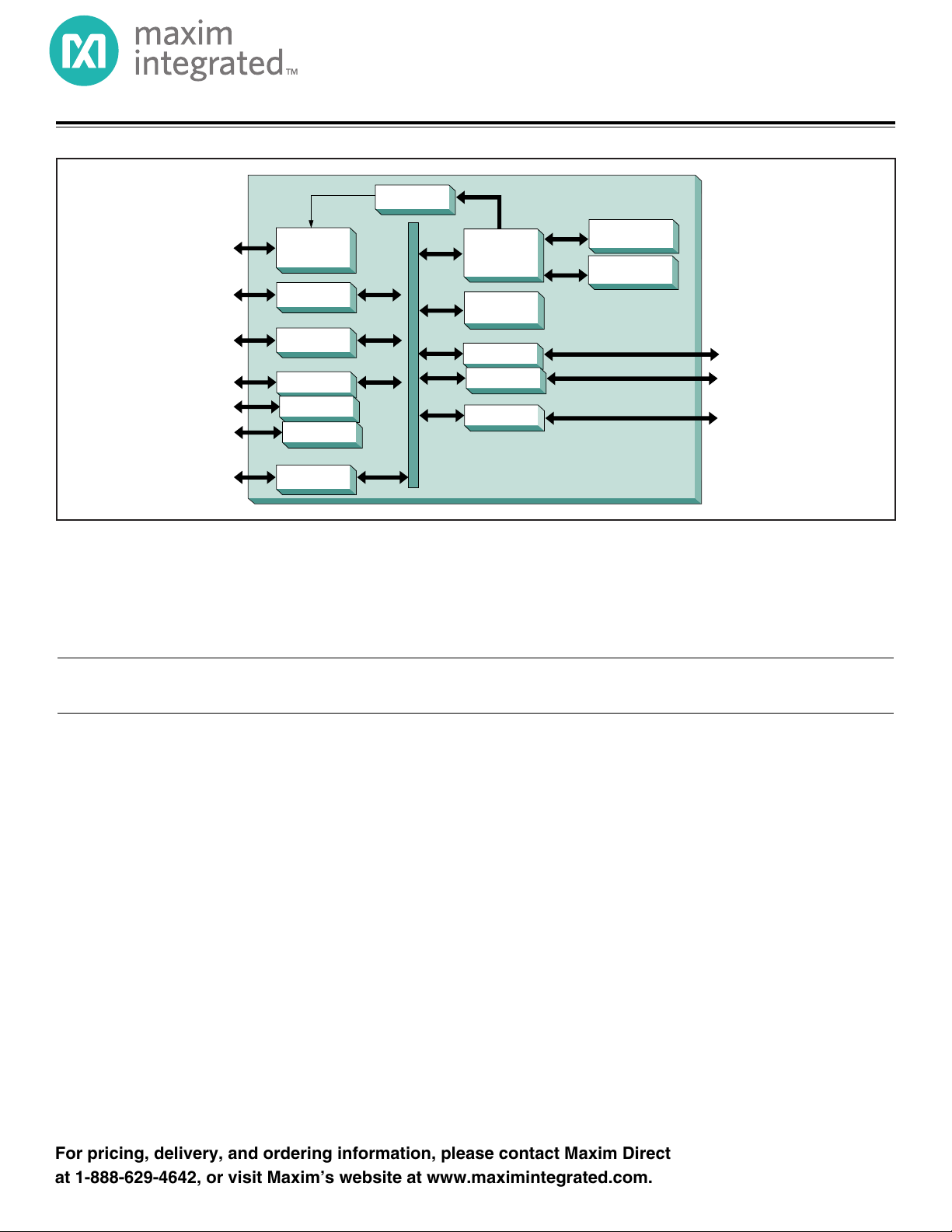
Figure 1. MAXQ2000 System and Peripheral Register Map
M0 M1 M2 M3 M4 M8 M9 M11 M12 M13 M14 M15
REAL-TIME
CLOCK
OWA
OWD
00h
01h
02h
03h
04h
05h
06h
07h
08h
09h
0Ah
0Bh
0Ch
0Dh
0Eh
0Fh
10h
11h
12h
13h
14h
15h
16h
17h
18h
19h
1Ah
1Bh
1Ch
1Dh
1Eh
1Fh
RESERVED
OR
OP CODE
PO0
PO4
PO1
PO5
PO2
PO6
PO3
PO7
PI0
PI4
PI1
PI5
PI2
PI6
PI3
PI7
PD0
PD4
PD1
PD5
PD2
PD6
PD3
PD7
RCNT
RTSS
RTSH
RTSL
RSSA
RASH
RASL
INTERRUPT
CONTROL
EIF0
EIF1
EIE0
EIE1
EIES0
EIES1
MA
MB
MC2
MC1
MC0
SERIAL
AND
SPI
LCD
CONTROLLER
TIMERS
ACC
ARRAY,
CONTROL
OTHER
FUNCTIONS
SCON0
SBUF0
SMD0
PR0
SPIB
SCON1
SBUF1
SMD1
PR1
SPICN
SPICF
SPICK
LCD15
LCD14
LCD13
LCD12
LCD11
LCD10
LCD9
LCD8
LCD7
LCD6
LCD5
LCD4
LCD3
LCD2
LCD1
LCD0
LCD16
LCFG
LCRA
T2CNA0 T2CNA1
T2H0 T2H1
T2RH0 T2RH1
T2CH0 T2CH1
T2CNA2
T2H2
T2RH2
T2CH2
T2CNB1
T2V1
T2R1
T2C1
T2CNB0 T2CNB2
T2V0 T2V2
T2R0 T2R2
T2C0 T2C2
T2CFG0 T2CFG1
T2CFG2
AP
APC
A[0]
A[1]
A[2]
A[3]
A[4]
A[5]
A[6]
A[7]
A[8]
A[9]
A[10]
A[11]
A[12]
A[13]
A[14]
A[15]
IP
SP
LC0
LC1
OFFS
DPC
GR
GRL
BP
GRS
GRH
GRXL
BP[offs]
DP0
DP1
PSF
CKCN
WDCN
SC
IC
IMR
IIR
IV
REGISTER MODULE
REGISTER INDEX
MC0R
PORT PINS
(GPIO)
HARDWARE
MULTIPLIER
MCNT
MC1R
PFX
Maxim Integrated
8
Page 9

Memory Organization
As with all MAXQ microcontrollers, the MAXQ2000 contains logically separate program and data memory spaces. All memory is internal, and physical memory segments (other than the stack and register memories) can be accessed as either program memory or as
data memory, but not both at once. The MAXQ2000 contains the following physical memory segments.
Register Space
As described in the MAXQ Family User’s Guide, register space on MAXQ microcontrollers consists of 16 register modules, each of
which can contain up to 32 registers. Of these possible 16 register modules, only 12 are used on the MAXQ2000—seven for system
registers and five for peripheral registers.
Program Stack
The MAXQ2000 provides a 16 x 16 hardware stack to support subroutine calls and system interrupts. This stack is used automatically by
CALL and RET instructions, and can also be accessed indirectly through the SP register as described in the MAXQ Family User’s Guide.
When using the in-circuit debugging features of the MAXQ2000, one word of the stack must be reserved to store the return location
when execution branches into the debugging routines in the utility ROM. If in-circuit debug will not be used, the entire stack is available for application use.
Data SRAM
The MAXQ2000 contains 1024 words (2kBytes) of on-chip data SRAM that can be mapped into either program or data space. The contents of this SRAM are indeterminate after power-on reset, but are maintained during Stop mode and across non-POR resets, as long
as the VDDsupply stays within the acceptable range.
When using the in-circuit debugging features of the MAXQ2000, the top 19 bytes (bytes 0x7ED to 0x7FF) of the SRAM must be
reserved for saved state storage and working space for the debugging routines in the utility ROM. If in-circuit debug will not be used,
the entire SRAM is available for application use.
Program Flash
The MAXQ2000 contains 32k x 16 of flash memory, which normally serves as program memory. When executing from the data SRAM or
utility ROM, this memory is mapped to data space (as 32kWords or 64kBytes) and can be used for lookup tables and similar functions.
Flash memory mapped into data space can be read from directly, like any other type of data memory. However, writing to flash memory
must be done indirectly by calling the in-application functions provided by the utility ROM. See the Utility ROM section for more details.
Program and Data Memory Mapping
Figures 2, 3, and 4 show the mapping of physical memory segments into the program and data memory space. The mapping of memory segments into program space is always the same. The mapping of memory segments into data space varies depending on which
memory segment is currently being executed from.
In all cases, whichever memory segment is currently being executed from in program space cannot be accessed in data space.
MAXQ Family User’s Guide:
MAXQ2000 Supplement
Maxim Integrated
9
Page 10

MAXQ Family User’s Guide:
MAXQ2000 Supplement
32k x 16
PROGRAM FLASH
OR MASKED ROM
PROGRAM
SPACE
EXECUTING FROM
DATA SPACE
(BYTE MODE)
DATA SPACE
(WORD MODE)
0000h
7FFFh
2k x 16
UTILITY ROM
87FFh
1k x 16
DATA SRAM
A000h
8000h
A3FFh
4k x 8
UTILITY ROM
8FFFh
8000h
2k x 8
DATA SRAM
0000h
07FFh
2k x 16
UTILITY ROM
87FFh
8000h
1k x 16
DATA SRAM
0000h
003FFh
Figure 2. Memory Map When Executing from Application Flash/ROM
Figure 3. Memory Map When Executing from Utility ROM
Maxim Integrated
10
PROGRAM
SPACE
1k x 16
DATA SRAM
2k x 16
UTILITY ROM
EXECUTING FROM
32k x 16
PROGRAM FLASH
OR MASKED ROM
A3FFh
A000h
87FFh
8000h
7FFFh
0000h
(BYTE MODE)
PROGRAM FLASH
OR MASKED ROM
DATA SPACE
64k x 8
PAGE 0
(IF CDA0 = 0)
PAGE 1
(IF CDA0 = 1)
2k x 8
DATA SRAM
FFFFh
8000h
07FFh
0000h
DATA SPACE
(WORD MODE)
32k x 16
PROGRAM FLASH
OR MASKED ROM
PAGES 0 AND 1
1k x 16
DATA SRAM
FFFFh
8000h
03FFh
0000h
Page 11
MAXQ Family User’s Guide:
MAXQ2000 Supplement
Clock Generation
All functional modules in the MAXQ2000 are synchronized to a single system clock. This system clock can be generated from one of
five possible sources (Figure 5):
• Internal ring oscillator
• Internal high-frequency oscillator using external crystal or resonator circuit
• External high-frequency clock signal
• Internal 32kHz oscillator using external crystal or resonator circuit
• External 32kHz clock signal
The MAXQ2000 does not provide the option for an external RC relaxation oscillator circuit.
Table 1 shows the registers and bits used to control clock generation and selection. For more information, see the register descriptions
in this guide and the MAXQ Family User’s Guide.
32k x 16
PROGRAM FLASH
OR MASKED ROM
PROGRAM
SPACE
EXECUTING FROM
DATA SPACE
(BYTE MODE)
DATA SPACE
(WORD MODE)
0000h
7FFFh
2k x 16
UTILITY ROM
87FFh
1k x 16
DATA SRAM
A000h
8000h
A3FFh
4k x 8
UTILITY ROM
8FFFh
8000h
64k x 8
PROGRAM FLASH
OR MASKED ROM
PAGE 0
(IF CDA0 = 0)
PAGE 1
(IF CDA0 = 1)
0000h
7FFFh
2k x 16
UTILITY ROM
87FFh
8000h
32k x 16
PROGRAM FLASH
OR MASKED ROM
PAGES 0 AND 1
0000h
7FFFh
Figure 4. Memory Map When Executing from Data SRAM
Maxim Integrated
11
Page 12
MAXQ Family User’s Guide:
MAXQ2000 Supplement
Table 1. System Clock Generation and Control Registers
External High-Frequency Oscillator Circuit or Clock
The high-frequency oscillator is the default source for system clock generation. This oscillator operates as described in the “Clock
Generation” section of Section 2: Architecture in the MAXQ Family User’s Guide. When using an external crystal or resonator circuit,
the circuit should be connected between the HFXIN and HFXOUT. When using an external clock signal to drive the high-frequency
clock, the external clock signal should be connected to the HFXIN pin, and the HFXOUT pin should be left unconnected.
Internal Ring Oscillator
The MAXQ2000 provides an internal ring oscillator that can be used as an alternate source for the system clock. This oscillator, which
requires no external components, typically runs at an 8MHz frequency. The exact frequency of the ring oscillator is not fixed and will
vary from part to part due to process variations, as well as over temperature and supply voltage for any given part.
REGISTER ADDRESS BIT FUNCTION
CKCN M8[0Eh]
Selects clock divide-by-1 (00), -2 (01), -4 (10), or -8 (11) mode.
CKCN M8[0Eh] 2 (PMME)
If set to 0, selects normal clock divide mode (as determined by CD[1:0]). If set to 1, selects
either divide-by-256 mode (when CD[1:0]=00) or 32kHz mode (when CD[1:0]=11).
CKCN M8[0Eh] 5 (RGMD)
Read-only. Indicates if ring oscillator (1) or external crystal/clock (0) is being used to provide
the system clock.
CKCN M8[0Eh] 6 (RGSL) Selects ring oscillator (1) or external crystal/clock (0) as the clock source.
RCNT M0[19h] 14 (X32D)
Disables (1) or enables (0) the internal 32kHz oscillator. If the 32kHz oscillator is disabled,
the RTC can be driven externally by a 32kHz clock input signal.
MAXQ2000
GLITCH-FREE
MUX
GLITCH-FREE
MUX
DIV 1
DIV 2
DIV 4
DIV 8
32kHz
PMM
CLOCK
DIVIDER
SELECTOR
WAKE-UP
ALARM
TIMERS
DEFAULT
RING SELECT
WATCHDOG
TIMER
RESET DOG
RWT
RESET
POWER-ON
RESET
STOP
STOP
POWER-ON
RESET
SWB
INTERRUPT/SERIAL PORT
RESET
STOP
RGSL
XDOG DONE
RGMD
POWER-ON RESET
WATCHDOG RESET
CLOCK
GENERATION
SYSTEM CLOCK
ENABLE
WATCHDOG INTERRUPT
RING
ENABLE
32kHz
CRYSTAL
CRYSTAL
MONITOR
ENABLE
INPUT
HF
CRYSTAL
CRYSTAL KLL
XDOG
STARTUP
TIMER
CLK INPUT
RESET XDOG COUNT
XDOG DONE
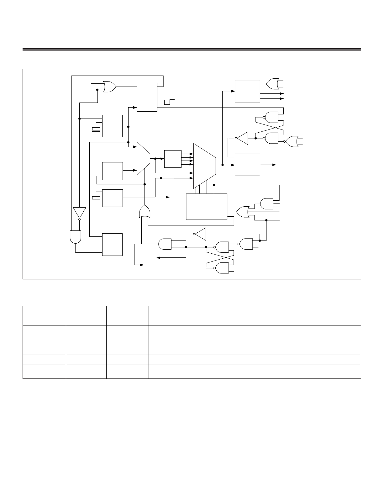
Figure 5. MAXQ2000 Clock Sources
Maxim Integrated
12
[1:0] to CD[1:0]
Page 13

To select the ring oscillator as the system clock source, the RGSL bit (CKCN.6) must be set to 1. Setting this bit immediately switches
over the system clock source to the ring oscillator. The RGMD (CKCN.5) bit indicates the current system clock source. If the ring oscillator is currently providing the system clock, RGMD equals 1; otherwise, RGMD equals 0.
Because the RGSL bit is cleared by power-on reset only, if this bit is set before entering Stop mode, the ring oscillator will still be used
as the system clock source when Stop mode is exited. In this case, a 4-cycle warmup delay is required when exiting Stop mode before
execution resumes using the ring oscillator as the system clock source.
When the system clock source is switched back from the ring oscillator to the high-frequency oscillator by clearing RGSL to zero, the
ring oscillator will still be used as the system clock source until the warmup period has completed for the high-frequency oscillator. This
will be reflected by the value of the RGMD bit, which remains at 1 until the warmup for the high-frequency oscillator has completed
and the clock switches over, at which point RGMD switches to 0.
External 32kHz Crystal Oscillator Circuit or Clock
The MAXQ2000 provides a 32kHz clock for use by the real-time clock module. This clock can be generated either by the internal 32kHz
crystal oscillator (using an external crystal) or by an external source. The 32kHz clock is also usable as a system clock source, a clock
for the LCD controller, and as an alternate Timer 2 clock.
The 32kHz crystal amplifier is switched off by default on power-on reset. With this crystal amplifier disabled, the 32kHz clock must be
provided directly by an external source. To use the 32kHz crystal amplifier to generate the 32kHz clock, the amplifier must be turned
on by setting the X32D (RCNT.14) bit to 0 and a 32.768kHz, 6pF crystal should be connected between the 32KIN and 32KOUT pins.
To use the 32kHz clock as a source for the system clock, Power Management Mode 2 must be entered by setting PMME, CD1, and
CD0 to 1. See the Power Management Features section for more details.
Interrupts
In general, interrupt handling on the MAXQ2000 operates as described in the MAXQ Family User’s Guide. All interrupt sources have
the same priority, and all interrupts cause program execution to branch to the location specified by the Interrupt Vector (IV) register,
which defaults to 0000h.
Table 2 lists all possible interrupt sources for the MAXQ2000, along with their corresponding module interrupt enable bits, local interrupt enable bits, and interrupt flags.
• Each module interrupt enable bit, when cleared to 0, will block interrupts originating in that module from being acknowledged.
When the module interrupt enable bit is set to 1, interrupts from that module are acknowledged (unless the interrupts have been
disabled globally).
• Each local interrupt enable bit, when cleared to 0, will disable the corresponding interrupt. When the local interrupt enable bit is set
to 1, the interrupt will be triggered whenever the interrupt flag is set to 1 (either by software or hardware).
• All interrupt flag bits cause the corresponding interrupt to trigger when the bit is set to 1. These bits are typically set by hardware
and must be cleared by software (generally in the interrupt handler routine).
Note that for an interrupt to fire, the following five conditions must exist:
•Interrupts must be enabled globally by setting IGE (IC.0) to 1.
• The module interrupt enable bit for that interrupt source’s module must be set to 1.
• The local interrupt enable bit for that specific interrupt source must be set to 1.
• The interrupt flag for that interrupt source must be set to 1. Typically, this is done by hardware when the condition that requires interrupt service occurs.
• The Interrupt In Service (INS) bit must be cleared to 0. This bit is set automatically upon vectoring to the interrupt handler (IV) address
and cleared automatically upon exit (RETI/POPI), so the only reason to clear this bit manually (inside the interrupt handler routine) is
to allow nested interrupt handling.
MAXQ Family User’s Guide:
MAXQ2000 Supplement
Maxim Integrated
13
Page 14

MAXQ Family User’s Guide:
MAXQ2000 Supplement
Table 2. MAXQ2000 Interrupt Sources and Control Bits
INTERRUPT MODULE ENABLE BIT LOCAL ENABLE BIT INTERRUPT FLAG
Watchdog Interrupt IMS (IMR.7) EWDI (WDCN.6) WDIF (WDCN.3)
External Interrupt 0 IM0 (IMR.0) EX0 (EIE0.0) IE0 (EIF0.0)
External Interrupt 1 IM0 (IMR.0) EX1 (EIE0.1) IE1 (EIF0.1)
External Interrupt 2 IM0 (IMR.0) EX2 (EIE0.2) IE2 (EIF0.2)
External Interrupt 3 IM0 (IMR.0) EX3 (EIE0.3) IE3 (EIF0.3)
External Interrupt 4 IM0 (IMR.0) EX4 (EIE0.4) IE4 (EIF0.4)
External Interrupt 5 IM0 (IMR.0) EX5 (EIE0.5) IE5 (EIF0.5)
External Interrupt 6 IM0 (IMR.0) EX6 (EIE0.6) IE6 (EIF0.6)
External Interrupt 7 IM0 (IMR.0) EX7 (EIE0.7) IE7 (EIF0.7)
External Interrupt 8 IM1 (IMR.1) EX8 (EIE1.0) IE8 (EIF1.0)
External Interrupt 9 IM1 (IMR.1) EX9 (EIE1.1) IE9 (EIF1.1)
External Interrupt 10* IM1 (IMR.1) EX10 (EIE1.2) IE10 (EIF1.2)
External Interrupt 11* IM1 (IMR.1) EX11 (EIE1.3) IE11 (EIF1.3)
External Interrupt 12 IM1 (IMR.1) EX12 (EIE1.4) IE12 (EIF1.4)
External Interrupt 13 IM1 (IMR.1) EX13 (EIE1.5) IE13 (EIF1.5)
External Interrupt 14 IM1 (IMR.1) EX14 (EIE1.6) IE14 (EIF1.6)
External Interrupt 15 IM1 (IMR.1) EX15 (EIE1.7) IE15 (EIF1.7)
RTC Time-of-Day Alarm IM0 (IMR.0) ADE (RCNT.1) ALDF (RCNT.6)
RTC Subsecond Alarm IM0 (IMR.0) ASE (RCNT.2) ALSF (RCNT.7)
Serial Port 0 Receive IM2 (IMR.2) ESI (SMD0.2) RI (SCON0.0)
Serial Port 0 Transmit IM2 (IMR.2) ESI (SMD0.2) TI (SCON0.1)
Serial Port 1 Receive IM3 (IMR.3) ESI (SMD1.2) RI (SCON1.0)
Serial Port 1 Transmit IM3 (IMR.3) ESI (SMD1.2) TI (SCON1.1)
SPI Mode Fault IM3 (IMR.3) ESPII (SPICF.7) MODF (SPICN.3)
SPI Write Collision IM3 (IMR.3) ESPII (SPICF.7) WCOL (SPICN.4)
SPI Receive Overrun IM3 (IMR.3) ESPII (SPICF.7) ROVR (SPICN.5)
SPI Transfer Complete IM3 (IMR.3) ESPII (SPICF.7) SPIC (SPICN.6)
Timer 0–Low Compare IM3 (IMR.3) ET2L (T2CNB0.7) T2CL (T2CNB0.0)
Timer 0–Low Overflow IM3 (IMR.3) ET2L (T2CNB0.7) TF2L (T2CNB0.2)
Timer 0–Capture/Compare IM3 (IMR.3) ET2 (T2CNA0.7) TCC2 (T2CNB0.1)
Timer 0–Overflow IM3 (IMR.3) ET2 (T2CNA0.7) TF2 (T2CNB0.3)
Timer 1–Low Compare IM4 (IMR.4) ET2L (T2CNB1.7) T2CL (T2CNB1.0)
Timer 1–Low Overflow IM4 (IMR.4) ET2L (T2CNB1.7) TF2L (T2CNB1.2)
Maxim Integrated
14
Page 15

MAXQ Family User’s Guide:
MAXQ2000 Supplement
Table 2. MAXQ2000 Interrupt Sources and Control Bits (continued)
INTERRUPT MODULE ENABLE BIT LOCAL ENABLE BIT INTERRUPT FLAG
Timer 1–Capture/Compare IM4 (IMR.4) ET2 (T2CNA1.7) TCC2 (T2CNB1.1)
Timer 1–Overflow IM4 (IMR.4) ET2 (T2CNA1.7) TF2 (T2CNB1.3)
Timer 2–Low Compare IM4 (IMR.4) ET2L (T2CNB2.7) T2CL (T2CNB2.0)
Timer 2–Low Overflow IM4 (IMR.4) ET2L (T2CNB2.7) TF2L (T2CNB2.2)
Timer 2–Capture/Compare IM4 (IMR.4) ET2 (T2CNA2.7) TCC2 (T2CNB2.1)
Timer 2–Overflow IM4 (IMR.4) ET2 (T2CNA2.7) TF2 (T2CNB2.3)
1-Wire Presence Detect*
IM3 (IMR.3);
EOWMI (OWD[5].7)
EPD (OWD[3].0) PD (OWD[2].0)
1-Wire Transmit Buffer Empty*
IM3 (IMR.3);
EOWMI (OWD[5].7)
ETBE (OWD[3].2) TBE (OWD[2].2)
1-Wire Transmit Shift Register Empty*
IM3 (IMR.3);
EOWMI (OWD[5].7)
ETMT (OWD[3].3) TEMT (OWD[2].3)
1-Wire Receive Buffer Full*
IM3 (IMR.3);
EOWMI (OWD[5].7)
ERBF (OWD[3].4) RBF (OWD[2].4)
1-Wire Receive Shift Register Full*
IM3 (IMR.3);
EOWMI (OWD[5].7)
ERSF (OWD[3].5) RSRF (OWD[2].5)
1-Wire Short*
IM3 (IMR.3);
EOWMI (OWD[5].7)
EOWSH (OWD[3].6) OW_SHORT (OWD[2].6)
1-Wire Low*
IM3 (IMR.3);
EOWMI (OWD[5].7)
EOWL (OWL[3].7) OW_LOW (OWD[2].7)
* External Interrupts 10, external interrupt 11, and 1-Wire are only available on the 68-pin (RAX) version of the MAXQ2000.
Note 1: For 1-Wire Master interrupts to be received, both IM3 and EOWMI must be set to 1.
Note 2: The notation OWD[n] refers to accessing the OWD register with the OWA register set to n.
Maxim Integrated
15
Page 16
MAXQ Family User’s Guide:
MAXQ2000 Supplement
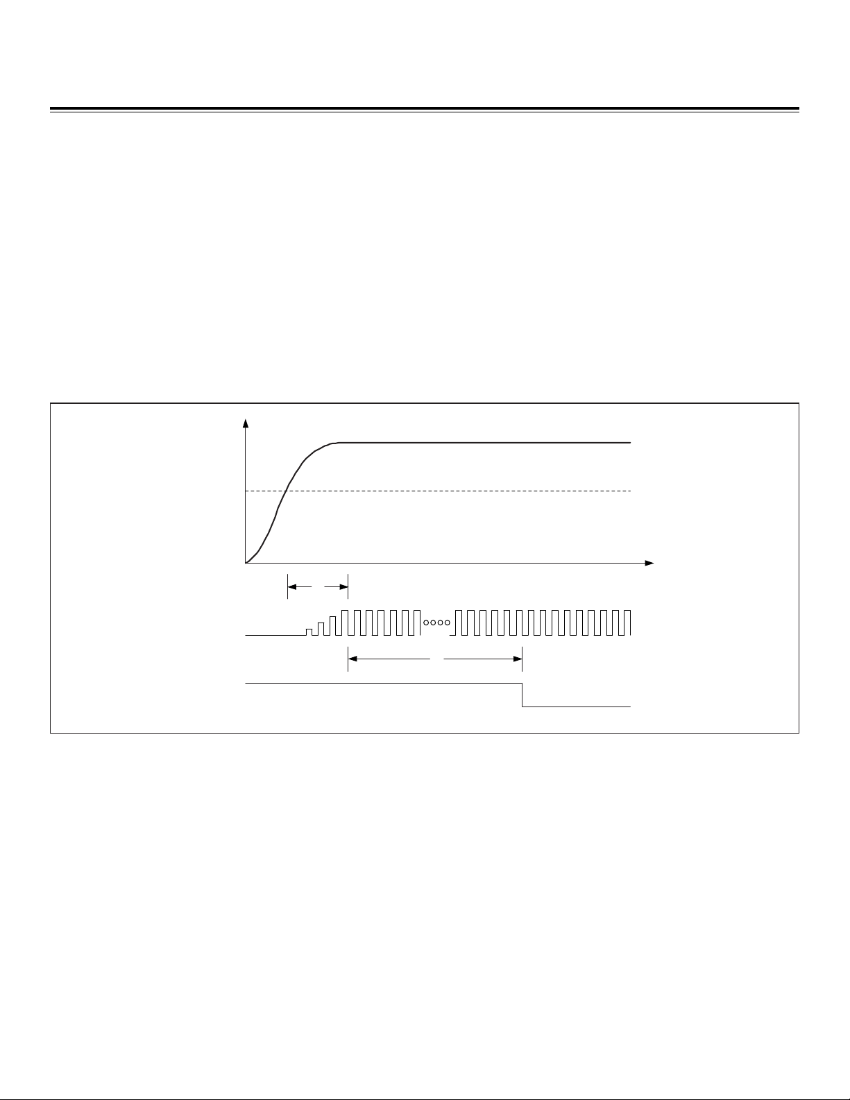
Reset Conditions
There are three possible reset sources for the MAXQ2000. While in the reset state, the enabled system clock oscillator continues running, but no code execution occurs. Once the reset condition has been removed or has completed, code execution resumes at
address 8000h for all reset types.
Power-On Reset
When power is first applied to the MAXQ2000, or when the internal supply voltage VDDdrops below the minimum allowed value, the
processor is held in a power-on reset state (Figure 6). For the MAXQ2000 to exit power-on reset, the following two conditions must apply:
•V
DD
is within the acceptable range for that power supply (see data sheet for values).
• The ring oscillator has completed 65,536 cycles (delay for power supply to stabilize).
Note that since the MAXQ2000 has no brownout reset function, the power-on reset is only guaranteed to occur if V
DD
drops all the way
to ground before rising again. Brownout events where VDDdrops partially (but remains above ground) and then rises back into the
acceptable range are not guaranteed to trigger a power-on reset and can result in unpredictable device behavior.
If the V
DDIO
power supply drops to ground, a power-on reset is not triggered. However, this causes all port pins driven by V
DDIO
to
drop to ground. Additionally, the 32kHz oscillator only operates when V
DDIO
is within acceptable limits.
Watchdog Timer Reset
The watchdog timer on the MAXQ2000 functions as described in the MAXQ Family User’s Guide. When running at 14MHz, the maximum watchdog time period before reset is approximately 150ms.
Since the RGSL bit is cleared to 0 on power-on reset only, it is possible to exit a watchdog reset with the clock source set to the highfrequency oscillator. In this case, execution resumes running from the ring oscillator, and the switchover to the high-frequency oscillator occurs automatically when the 65,536-cycle warmup delay for that oscillator has completed.
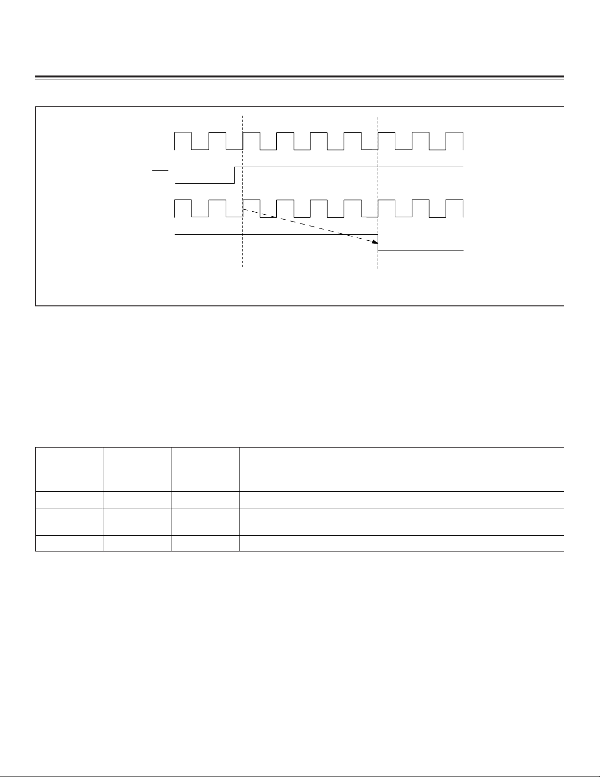
External Reset
External reset via RESET is a synchronous reset source. After the external reset low has been removed and sampled, execution
resumes (running from the ring oscillator) following a delay of four ring-oscillator cycles, as shown in Figure 7.
Since the RGSL bit is cleared to 0 on power-on reset only, it is possible to exit an external reset with the clock source set to the highfrequency oscillator. In this case, execution resumes running from the ring oscillator, and the switchover to the high-frequency oscillator occurs automatically when the 65,536-cycle warmup delay for that oscillator has completed.
V
DD(MIN)
T1
RING
OSCILLATOR
INTERNAL
RESET
T2
(T1 = STARTUP TIME FOR RING OSCILLATOR)
(T2 = 65,536 RING OSCILLATOR CYCLES, OR 8.192ms AT 8MHz)
Figure 6. MAXQ2000 Power-On Reset
Maxim Integrated
16
Page 17
Power Management Features
The MAXQ2000 provides the following features to assist in power management.
• Divide-by-256 (PMM1) and 32kHz (PMM2) modes to reduce current consumption.
• Switchback mode to exit PMM modes automatically when rapid processing is required.
• Ultra-low-power Stop mode.
Table 3 shows the system registers and bits used to control power management features. For more information, refer to the register
descriptions in the MAXQ Family User’s Guide.
Table 3. System Power Management Registers
Divide-by-256 Mode (PMM1)
In this power management mode, all operations continue as normal but at a reduced clock rate (the high-frequency system clock divided by 256). This power management mode affects module clock rates as follows.
•Program execution occurs at the high-frequency clock rate divided by 256.
• The RTC module continues to operate using its originally selected clock, which is either the 32kHz clock or the high-frequency clock
divided by 128, as selected by the ACS bit (RCNT.13).
• The LCD module continues to operate using its originally selected clock, which is either the 32kHz clock or the high-frequency clock
divided by 128, as selected by the LCCS bit (LCRA.6).
• All other functional modules (timers, UARTs, SPI) operate at the high-frequency clock rate divided by 256.
MAXQ Family User’s Guide:
MAXQ2000 Supplement
CLOCK
RESET
RESET
SAMPLING
INTERNAL
RESET
FIRST
INSTRUCTION
FETCH
Figure 7. MAXQ2000 External Reset
REGISTER ADDRESS BIT FUNCTION
CKCN M8[0Eh]
Selects clock divide-by-1 (00), -2 (01), -4 (10), or -8 (11) mode. When PMM mode is
enabled, selects divide-by-256 (00) or 32kHz (11) mode.
CKCN M8[0Eh] 2 (PMME) Selects PMM mode (when set to 1) or normal clock divide mode (when set to 0).
CKCN M8[0Eh] 3 (SWB)
When set to 1, enables automatic switchback from PMM (divide-by-256 mode) to normal
clock divide mode under certain conditions.
CKCN M8[0Eh] 4 (STOP) When set to 1, causes the processor to enter Stop mode.
Maxim Integrated
17
[1:0] to CD[1:0]
Page 18

MAXQ Family User’s Guide:
MAXQ2000 Supplement
This power management mode is entered by setting the PMME bit (CKCN.2) to 1 while the CD1 and CD0 (CKCN[1:0]) bits are both
cleared to 0. When PMM1 mode is exited (either by clearing the PMME bit or as a result of a switchback trigger), system operation will
revert to the mode indicated by the values of the CD1 and CD0 bits, which in this case will be the standard divide-by-1 clock mode.
32kHz Mode (PMM2)
In this power management mode, all operations continue as normal using the 32kHz clock as the system clock source. This power
management mode affects module clock rates as follows.
•Program execution occurs at the 32kHz clock rate.
• The RTC module continues to operate using its originally selected clock, which is either the 32kHz clock or the high-frequency clock
divided by 128, as selected by the ACS bit (RCNT.13).
• The LCD module continues to operate using its originally selected clock, which is either the 32kHz clock or the high-frequency clock
divided by 128, as selected by the LCCS bit (LCRA.6).
• All other functional modules (timers, UARTs, SPI) operate at the 32kHz clock rate.
This power management mode is entered by setting the PMME bit (CKCN.2) to 1 while the CD1 and CD0 (CKCN[1:0]) bits are both
set to 1. When PMM2 mode is exited (either by clearing the PMME bit or as a result of a switchback trigger), system operation will revert
to the mode indicated by the values of the CD1 and CD0 bits, which in this case will be the divide-by-8 clock mode.
When PMM2 mode is entered, the high-frequency oscillator is automatically disabled unless Switchback has been enabled by setting
the SWB bit to 1. If Switchback is not being used, the LCD module and RTC module should both be set to use the 32kHz clock (not
HFClk / 128) before PMM2 mode is entered.
Switchback Mode
As described in the MAXQ Family User’s Guide, Switchback mode provides automatic exit from power management mode when a
higher clock rate is required to respond to I/O, such as UART activity, SPI activity, or an external interrupt.
Switchback mode is enabled when the SWB (CKCN.3) bit is set to 1 and the PMME (CKCN.2) bit is set to 1(the system is in either the
PMM1 or PMM2 modes). If Switchback is enabled, the PMME bit will be cleared (causing the system to exit power management mode)
when any of the following conditions occur.
• An external interrupt condition occurs on an INTx pin and the corresponding external interrupt is enabled.
• An active-low transition occurs on the RXD0 or RXD1 pin and the corresponding UART is enabled to receive data. If PMM2 mode is
exited in this manner, the first character read by the UART will be received incorrectly.
• The SBUF0 or SBUF1 register is written to transmit a byte and the corresponding UART is enabled to transmit data.
• The SPIB register is written to send an outgoing byte through the SPI interface and transmission is enabled.
• An active-low transition occurs on the SSEL pin when the SPI interface is configured for slave mode.
•A Time-of-Day alarm is generated by the RTC module.
• Active debug mode is entered either by a breakpoint match or direct issuance of the Debug command from background mode.
As described in the MAXQ Family User’s Guide, if any of these conditions are true (a Switchback source is active) and the SWB bit has
been set, the PMME bit cannot be set to enter power management mode.
Stop Mode
Stop mode disables all circuits within the MAXQ2000 except for the 32kHz crystal amplifier and any circuitry that is clocked directly
by the 32kHz clock. All other on-chip clocks, timers, serial ports, and other peripherals are stopped, and no code execution occurs.
Once in Stop mode, the MAXQ2000 is in a mostly static state, with power consumption determined largely by leakage currents.
Stop mode is invoked by setting the STOP bit to 1. The MAXQ2000 enters Stop mode immediately when the STOP bit is set. Entering
Stop mode does not affect the setting of the clock control bits; this allows the system to return to its original operating frequency following Stop mode removal.
The processor exits Stop mode if any of the following conditions occur.
• External reset (from the RST pin)
•Power-on reset
• External interrupt (interrupt must be enabled prior to entering Stop mode)
•RTC time-of-day alarm
Maxim Integrated
18
Page 19

Note that exiting Stop mode through external reset or power-on reset causes the processor to undergo a normal reset cycle, as
opposed to resuming execution at the point at which it entered Stop mode. Exiting Stop mode by means of an external interrupt or
time-of-day alarm causes the processor to resume execution at the instruction following the one that set the STOP bit.
When Stop mode is exited, processor execution resumes as follows.
• If the ring oscillator is selected as the system clock source (RGSL = 1), execution resumes using the ring oscillator as the system
clock following a delay of four ring cycles.
• If the high-frequency oscillator is selected as the system clock source (RGSL = 0), execution resumes using the ring oscillator as the
system clock following a delay of four ring cycles. After the high-frequency oscillator has completed its warmup period, the system
clock source switches over to the high-frequency clock automatically.
• If the 32kHz oscillator is selected as the system clock source, execution resumes using the 32kHz oscillator as the system clock fol-
lowing a delay of four ring cycles. For this to work properly, the 32kHz crystal amplifier must be enabled and running prior to entering Stop mode, or an external 32kHz clock must be provided immediately upon Stop mode exit (if X32D is set to 1).
ADDENDUM TO SECTION 3: PROGRAMMING
Refer to Section 3: Programming in the MAXQ Family User’s Guide for examples of general program operations involving the MAXQ
core. The MAXQ2000 contains the MAXQ20 (16-bit accumulator version) of the MAXQ core.
ADDENDUM TO SECTION 4: SYSTEM REGISTER DESCRIPTIONS
Refer to Section 4: System Register Descriptions in the MAXQ Family User’s Guide for functional descriptions of the registers and bits
listed in Tables 4, 5, and 6.
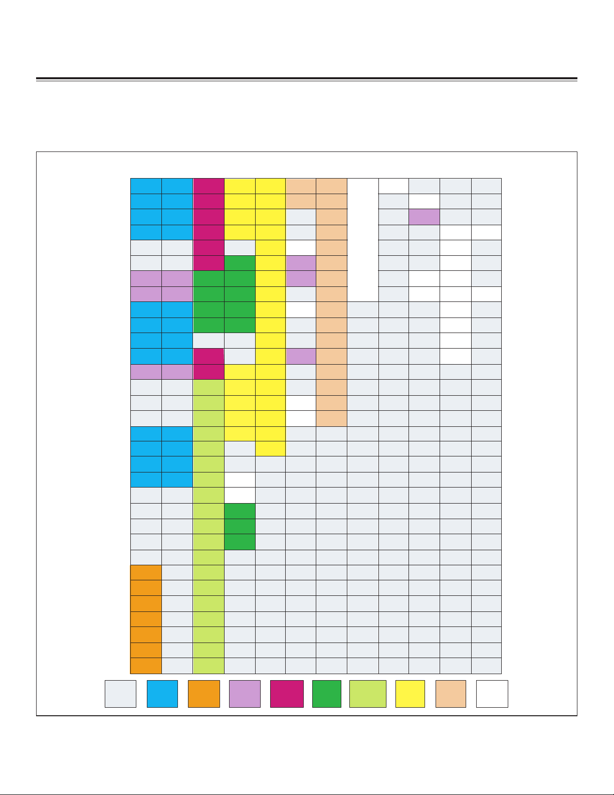
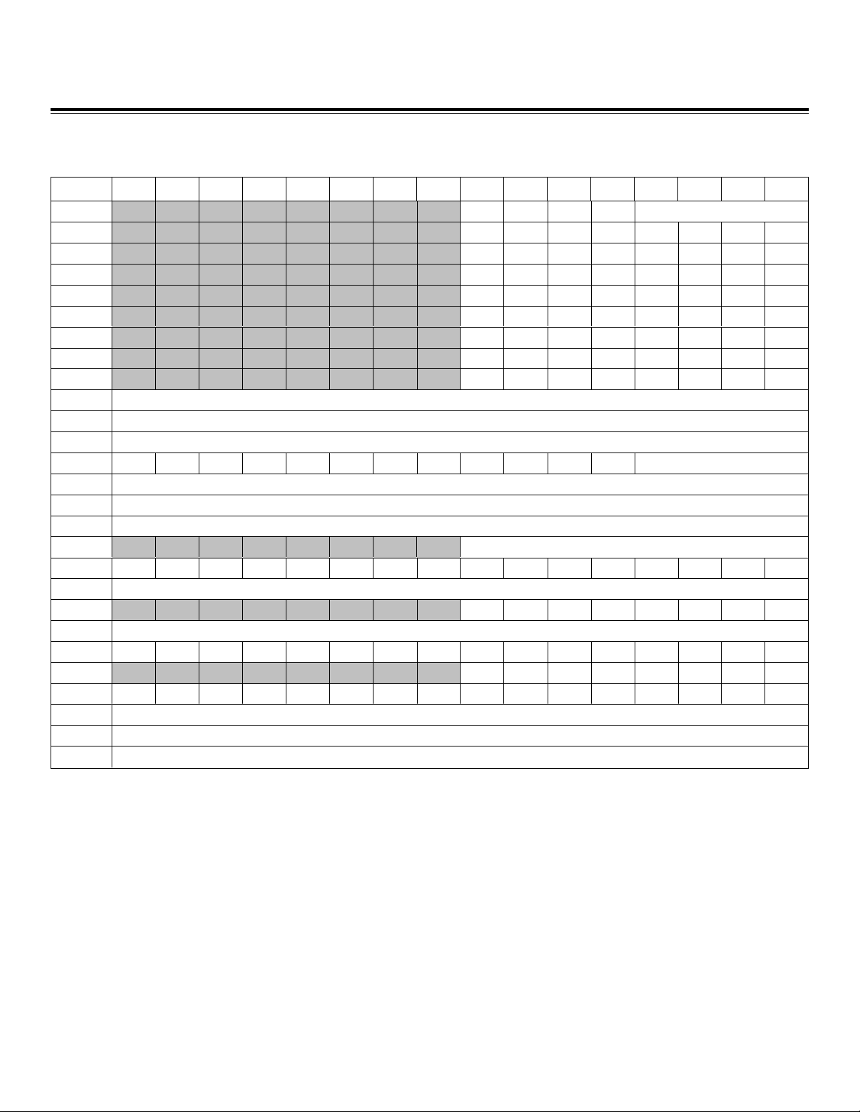
Table 4. System Register Map
Note: Register names that appear in italics indicate read-only registers. Register names that appear in bold indicate 16-bit registers. All other registers are 8
bits in width.
MAXQ Family User’s Guide:
MAXQ2000 Supplement
CYCLES TO
READ
CYCLES TO
WRITE
REGISTER
INDEX
AP (8h) A (9h) PFX (Bh) IP (Ch) SP (Dh) DPC (Eh) DP (Fh)
1 1 0xh AP A[0]
PFX IP
1 1 1xh APC A[1]
SP
1 1 2xh — A[2]
IV
1 1 3xh — A[3] Offs
DP[0]
1 1 4xh PSF A[4]
DPC
1 1 5xh IC A[5]
GR
1 1 6xh IMR A[6]
LC[0]
GRL
1 1 7xh — A[7]
LC[1] BP DP[1]
1 2 8xh SC A[8]
GRS
1 2 9xh — A[9] GRH
1 2 Axh — A[10]
GRXL
12BxhIIR A[11]
FP
1 2 Cxh — A[12]
1 2 Dxh — A[13]
1 2 Exh CKCN A[14]
1 2 Fxh WDCN A[15]
Maxim Integrated
19
Page 20
MAXQ Family User’s Guide:
MAXQ2000 Supplement
Table 5. System Register Bit Functions
REG
BIT 0
AP — — — — AP (4 bits)
APC
IDS — — —
MOD0
PSF ZS—
OV C E
IC ——
———INS
IGE
IMR
——
IM0
SC
——
—
—
IIR IIS — — II4 II3 II2 II1 II0
CKCN —
CD0
WDCN
RWT
A[0..15]
A[n] (16 bits)
PFX PFX (16 bits)
IP IP (16 bits)
SP ———————————— SP (4 bits)
IV IV (16 bits)
LC[0] LC[0] (16 bits)
LC[1] LC[1] (16 bits)
Offs Offs (8 bits)
DPC ———————————
SDPS0
GR GR (16 bits)
GRL
GR.0
BP BP (16 bits)
GRS
GR.8
GRH
GR.8
GRXL
GR.0
FP FP (16 bits)
DP[0] DP[0] (16 bits)
DP[1] DP[1] (16 bits)
Maxim Integrated
20
BIT 15 BIT 14 BIT 13 BIT 12 BIT 11 BIT 10 BIT 9 BIT 8 BIT 7 BIT 6 BIT 5 BIT 4 BIT 3 BIT 2 BIT 1
GR.7 GR.6 GR.5 GR.4 GR.3 GR.2 GR.1 GR.0 GR.15 GR.14 GR.13 GR.12 GR.11 GR.10 GR.9
GR.7 GR.7 GR.7 GR.7 GR.7 GR.7 GR.7 GR.7 GR.7 GR.6 GR.5 GR.4 GR.3 GR.2 GR.1
CLR
GPF1 GPF0
CGDS
IMS
TAP
RGSL RGMD STOP SWB PMME CD1
POR EWDI WD1 WD0 WDIF WTRF EWT
GR.7 GR.6 GR.5 GR.4 GR.3 GR.2 GR.1
GR.15 GR.14 GR.13 GR.12 GR.11 GR.10 GR.9
IM4 IM3 IM2 IM1
CDA0
WBS2 WBS1 WBS0 SDPS1
MOD2 MOD1
ROD PWL
Page 21

Table 6. System Register Reset Values
MAXQ Family User’s Guide:
MAXQ2000 Supplement
REG
BIT 0
AP 00000000
APC 00000000
PSF 10000000
IC 00000000
IMR 00000000
SC 000000s 0
IIR 00000000
CKCN 0 ss00000
WDCN ss000ss0
0000000000000000
PFX 0000000000000000
IP 1000000000000000
SP 0000000000001111
IV 0000000000000000
LC[0] 0000000000000000
LC[1] 0000000000000000
Offs 00000000
DPC0000000000011100
GR 0000000000000000
GRL 00000000
BP 0000000000000000
GRS0000000000000000
GRH 00000000
GRXL 0000000000000000
FP 0000000000000000
DP[0] 0000000000000000
DP[1] 0000000000000000
Note: Bits marked as “s” have special behavior upon reset; see register descriptions for details.
Maxim Integrated
21
BIT 15 BIT 14 BIT 13 BIT 12 BIT 11 BIT 10 BIT 9 BIT 8 BIT 7 BIT 6 BIT 5 BIT 4 BIT 3 BIT 2 BIT 1
A[0..15]
Page 22

MAXQ Family User’s Guide:
MAXQ2000 Supplement
The following section details the functionality of any System Registers contained in the MAXQ2000 that operate differently from their
descriptions in the MAXQ Family User’s Guide.
Register Name: IMR
Register Description: Interrupt Mask Register
Register Address: AP[06h]
The first five bits in this register are interrupt mask bits for modules 0 through 4, one bit per module. The eighth bit, IMS, serves as a
mask for any system module interrupt sources. Setting a mask bit allows the enabled interrupt sources for the associated module or system (with IMS) to generate interrupt requests. Clearing the mask bit effectively disables all interrupt sources associated with that module or, in the case of IMS, all system interrupt sources. The IMR register is intended to facilitate user-definable interrupt prioritization.
Bit 0: (IMR.0) Module 0 Interrupt Mask (IM0)
Bit 1: (IMR.1) Module 1 Interrupt Mask (IM1)
Bit 2: (IMR.2) Module 2 Interrupt Mask (IM2)
Bit 3: (IMR.3) Module 3 Interrupt Mask (IM3)
Bit 4: (IMR.4) Module 4 Interrupt Mask (IM4)
Bits 5 and 6: (IMR.5 and IMR.6) Reserved
Bit 7: (IMR.7) System Module Interrupt Mask (IMS)
Register Name: SC
Register Description: System Control Register
Register Address: AP[08h]
Bit 0: (SC.0) Reserved
Bit 1: (SC.1) Password Lock (PWL). This bit defaults to 1 on power-on reset only. When this bit is 1, it requires a 32-byte password
to be matched with the password in the program space before allowing access to the ROM Loader’s utilities for read/write of program
memory and debug functions. Clearing this bit to 0 disables the password protection to the ROM Loader.
Bits 2 and 3: (SC.2 and SC.3) Reserved
Bit 4: (SC.4) Code Data Access Bit 0 (CDA0). If this bit is set to 0, the lower half of physical program memory will be visible in data
space (when not executing from physical program memory) in byte mode. If this bit is set to 1, the upper half of physical program memory will be visible in data space in byte mode. When accessing data space in word mode, this bit has no effect.
Bit # 76543210
Name IMS — — IM4 IM3 IM2 IM1 IM0
Reset 00000000
Access r/w r r r/w r/w r/w r/w r/w
Bit # 7 6 5 43210
Name TAP — — CDA0 — — PWL —
Reset 1 0 0 0 0 0 not set 0
POR 10000010
Access r/w r r r/w r r r/w r
Maxim Integrated
22
Page 23

Bits 5 and 6: (SC.5 and SC.6) Reserved
Bit 7: (SC.7) Test Access (JTAG) Port Enable
0 = JTAG TAP functions are disabled and P4.0 through P4.3 can be used as general-purpose I/O pins.
1 = TAP special function pins P4.0 through P4.3 are enabled to act as JTAG inputs and outputs.
Register Name: IIR
Register Description: Interrupt Identification Register
Register Address: AP[0Bh]
The first five bits in this register indicate interrupts pending in modules 0 through 4, one bit per module. The eighth bit, IIS, indicates a
pending system interrupt (from the watchdog timer or other system function). The interrupt pending flags will be set only for enabled
interrupt sources waiting for service. The interrupt pending flag will be cleared when the pending interrupt source(s) within that module are disabled when the interrupt flag(s) are cleared by software.
Bit 0: (IIR.0) Interrupt Pending Flag for Module 0 (II0)
Bit 1: (IIR.1) Interrupt Pending Flag for Module 1 (II1)
Bit 2: (IIR.2) Interrupt Pending Flag for Module 2 (II2)
Bit 3: (IIR.3) Interrupt Pending Flag for Module 3 (II3)
Bit 4: (IIR.4) Interrupt Pending Flag for Module 4 (II4)
Bits 5 and 6: (IIR.5 and IIR.6) Reserved
Bit 7: (IIR.7) Interrupt Pending Flag for System Modules
Register Name: CKCN
Register Description: System Clock Control Register
Register Address: AP[0Eh]
The CKCN register bit settings determine the system clock source and clock divider as described in the following table.
MAXQ Family User’s Guide:
MAXQ2000 Supplement
Bit # 76543210
Name IIS — — II4 II3 II2 II1 II0
Reset 0 0 0 00000
Access r r r rrrrr
Bit # 76543210
Name — RGSL RGMD STOP SWB PMME CD1 CD0
Reset 0 0 s 00000
Access r/w r/w r r/w r/w r/w special special
Maxim Integrated
23
Page 24

MAXQ Family User’s Guide:
MAXQ2000 Supplement
MAXQ2000 System Clock Modes
Bit 0: (CKCN.0) Clock Divide 0 (CD0); Bit 1: (CKCN.1) Clock Divide 1 (CD1); Bit 2: (CKCN.2) Power Management Mode Enable
(PMME). These three bits control the divide ratio or enable power management mode for the system clock as shown in the MAXQ2000
System Clock Modes table. CD0 and CD1 can always be read, and they can be written as long as PMME = 0.
Setting the PMME bit to 1 activates either the divide-by-256 power management mode or the 32kHz power management mode,
depending on the settings of CD1 and CD0. When PMME is set to 1, CD0 and CD1 cannot be changed; their values will determine the
clock divide ratio that is used when the processor exits power management mode. When the 32kHz power management mode is
active, the high-frequency oscillator amplifier is disabled unless Switchback is enabled.
RGMD SWB PMME
CD1
CD0 SYSTEM CLOCK HIGH-FREQUENCY OSCILLATOR SWITCHBACK
0 0 0 0 0 HFOsc / 1 Running N/A
0 0 0 0 1 HFOsc / 2 Running N/A
0 0 0 1 0 HFOsc / 4 Running N/A
0 0 0 1 1 HFOsc / 8 Running N/A
0 0 1 0 0 HFOsc / 256 Running Not Active
0 1 1 0 0 HFOsc / 256 Running Active
1 0 0 0 0 Ring / 1 Off or Warming Up N/A
1 0 0 0 1 Ring / 2 Off or Warming Up N/A
1 0 0 1 0 Ring / 4 Off or Warming Up N/A
1 0 0 1 1 Ring / 8 Off or Warming Up N/A
1 0 1 0 0 Ring / 256 Off or Warming Up N/A
x 0 1 1 1 32kHz Off Not Active
x 1 1 1 1 32kHz Running Active
Maxim Integrated
24
Page 25

Bit 3: (CKCN.3) Switchback Enable (SWB). Setting this bit to 1 enables Switchback mode. If power management mode (either divide
by 256 or 32kHz) is active and Switchback is enabled, the PMME bit will be cleared to 0 when any of the following conditions occur.
• An external interrupt is generated based on an edge detect.
• Either serial port 0 or serial port 1 is enabled to receive data and detects a low condition on its data receive pin.
• Either serial port 0 or serial port 1 is enabled to transmit data has a byte written to its buffer register by software.
• The SPI module is enabled in slave mode and receives a slave select signal from the bus master.
• The SPI module is enabled to transmit data and has a byte written to its buffer register by software.
• A time-of-day interrupt occurs from the real-time clock.
• Debug mode is entered through command entry or a breakpoint match.
Triggering a Switchback condition only clears the PMME bit; the settings of CD0 and CD1 remain the same. This means that exiting
Switchback from divide-by-256 mode will revert to a divide by 1 mode, while exiting Switchback from 32kHz mode will revert to a divide
by 8 mode.
When either power management mode is active, the SWB bit may not be set to 1 as long as any of the above conditions are true.
Bit 4: (CKCN.4) Stop Mode Select (STOP). Setting this bit to 1 causes the processor to enter Stop Mode. This will not change the currently selected clock divide ratio.
Bit 5: (CKCN.5) Ring Oscillator Mode (RGMD). This read-only bit indicates the current oscillator source. If RGMD is set to 1, the internal ring oscillator is currently acting as the oscillator source for the system clock. (This can either be because RGSL = 1, or because
RGSL = 0, and the crystal warmup period has not yet completed.) If RGMD is cleared to 0, the external crystal oscillator is currently
acting as the oscillator source for the system clock (unless the PMM2 32kHz mode is active).
Bit 6: (CKCN.6) Ring Oscillator Select (RGSL). If this bit is set to 1, the ring oscillator will immediately begin sourcing the system
clock, and the high-frequency oscillator will be disabled (unless 32kHz mode and Switchback are enabled). Clearing this bit to 0
enables the high-frequency oscillator. Until the warmup period for the high-frequency oscillator has completed, the ring oscillator will
still provide the system clock source (indicated by RGMD = 1). Once the warmup period completes, the system clock source will automatically switch over to the high-frequency oscillator, and RGMD will go to 0.
Bit 7: (CKCN.7) Reserved
MAXQ Family User’s Guide:
MAXQ2000 Supplement
Maxim Integrated
25
Page 26

MAXQ Family User’s Guide:
MAXQ2000 Supplement
ADDENDUM TO SECTION 5: PERIPHERAL REGISTER MODULES
Refer to the MAXQ Family User’s Guide.
Table 7. Peripheral Register Map
CYCLES TO
READ
CYCLES TO
WRITE
REGISTER
INDEX
M0
(0h)
M1
(1h)
M2
(2h)
M3
(3h)
M4
(4h)
M5
(5h)
1 1 00h PO0 PO4 MCNT T2CNA0 T2CNA1 —
1 1 01h PO1 PO5
MA
T2H0 T2H1 —
1 1 02h PO2 PO6
MB
T2RH0 T2RH1 —
1 1 03h PO3 PO7
MC2
T2CH0 T2CH1 —
1 1 04h — —
MC1
— T2CNA2 —
1 1 05h — —
MC0 SPIB
T2H2 —
1 1 06h EIF0 EIF1 SCON0 SCON1 T2RH2 —
1 1 07h EIE0 EIE1 SBUF0 SBUF1 T2CH2 —
1 2 08h PI0 PI4 SMD0 SMD1 T2CNB1 —
1 2 09h PI1 PI5
PR0 PR1 T2V1
—
1 2 0Ah PI2 PI6 ——
T2R1
—
1 2 0Bh PI3 PI7
MC1R
—
T2C1
—
1 2 0Ch EIES0 EIES1
MC0R
T2CNB0 T2CNB2 —
1 2 0Dh — —
LCRA T2V0 T2V2
—
1 2 0Eh — — LCFG
T2R0 T2R2
—
1 2 0Fh — — LCD16
T2C0 T2C2
—
2 2 10h PD0 PD4 LCD0 T2CFG0 T2CFG1 —
2 2 11h PD1 PD5 LCD1 — T2CFG2 —
2 2 12h PD2 PD6 LCD2 — —
2 2 13h PD3 PD7 LCD3 OWA —
2 2 14h — — LCD4 OWD —
2 2 15h — — LCD5 SPICN —
2 2 16h — — LCD6 SPICF —
2 2 17h — — LCD7 SPICK —
2 2 18h — — LCD8 — —
2 2 19h
RCNT
— LCD9 — —
2 2 1Ah RTSS — LCD10 — —
2 2 1Bh
RTSH
— LCD11 ICDF —
2 2 1Ch
RTSL
— LCD12 — —
2 2 1Dh RSSA — LCD13 — —
2 2 1Eh RASH SVS LCD14 — —
2 2 1Fh
RASL
WKO LCD15 — —
Note: Register names in italics indicate read-only registers. Register names in bold indicate 16-bit registers. All other registers are 8 bits in width.
Maxim Integrated
26
Page 27
MAXQ Family User’s Guide:
MAXQ2000 Supplement
REG BIT 15
BIT 0
PO0 PO0 (8 bits)
PO1 PO1 (8 bits)
PO2 PO2 (8 bits)
PO3 PO3 (8 bits)
EIF0 IE7 IE6 IE5 IE4 IE3 IE2 IE1 IE0
EIE0 EX7 EX6 EX5 EX4 EX3 EX2 EX1 EX0
PI0 PI0 (8 bits)
PI1 PI1 (8 bits)
PI2 PI2 (8 bits)
PI3 PI3 (8 bits)
EIES0 IT7 IT6 IT5 IT4 IT3 IT2 IT1 IT0
PD0 PD0 (8 bits)
PD1 PD1 (8 bits)
PD2 PD2 (8 bits)
PD3 PD3 (8 bits)
RCNT WE
——— — —
RDY
ASE ADE
RTCE
RTSS RTSS (8 bits)
RTSH RTSH (16 bits)
RTSL RTSL (16 bits)
RSSA RSSA (8 bits)
RASH RASH (8 bits)
RASL RASL (16 bits)
PO4 — — — PO4 (5 bits)
PO5 PO5 (8 bits)
PO6 PO6 (8 bits)
PO7 — — — — — — PO7 (2 bits)
EIF1 IE15 IE14 IE13 IE12 IE11 IE10 IE9 IE8
EIE1 EX15 EX14 EX13 EX12
EX9 EX8
PI4 — — — PI4 (5 bits)
PI5 PI5 (8 bits)
PI6 PI6 (8 bits)
PI7 — — — — — — PI7 (2 bits)
EIES1 IT15 IT14 IT13 IT12 IT11 IT10 IT9 IT8
PD4 — — — PD4 (5 bits)
PD5 PD5 (8 bits)
Table 8. Peripheral Register Bit Functions
Maxim Integrated
27
BIT 14 BIT 13 BIT 12 BIT 11 BIT 10 BIT 9 BIT 8 BIT 7 BIT 6 BIT 5 BIT 4 BIT 3 BIT 2 BIT 1
X32D ACS
ALSF ALDF RDYE
BUSY
EX11 EX10
Page 28
MAXQ Family User’s Guide:
MAXQ2000 Supplement
REG BIT15
BIT14
BIT13
BIT12
BIT11
BIT 10
BIT 9
BIT 8
BIT 7
BIT 6
BIT 5
BIT 4
BIT 3
BIT 2
BIT 1
BIT 0
PD6
PD6 (8 bits)
PD7
— — — — — — PD7 (2 bits)
SVS
SV67
SV65 SV64 — — SV71
SV70
WKO
— — — — — WKL
WKE0
MCNT
OF — — SQU
CLD
SUS
MA
MA (16 bits)
MB
MB (16 bits)
MC2
MC2 (16 bits)
MC1
MC1 (16 bits)
MC0
MC0 (16 bits)
SCON0
SM1 SM2 REN TB8 RB8 TI RI
SBUF0
SBUF0 (8 bits)
SMD0
—————ESI0
FEDE0
PR0
PR0 (16 bits)
MC1R
MC1R (16 bits)
MC0R
MC0R (16 bits)
LCRA
———
LRIG
LRA0
LCFG
— — OPM DPE
LCD0
LCD0 (8 bits)
LCD1
LCD1 (8 bits)
LCD2
LCD2 (8 bits)
LCD3
LCD3 (8 bits)
LCD4
LCD4 (8 bits)
LCD5
LCD5 (8 bits)
LCD6
LCD6 (8 bits)
LCD7
LCD7 (8 bits)
LCD8
LCD8 (8 bits)
LCD9
LCD9 (8 bits)
LCD10
LCD10 (8 bits)
LCD11
LCD11 (8 bits)
LCD12
LCD12 (8 bits)
LCD13
LCD13 (8 bits)
LCD14
LCD14 (8 bits)
LCD15
LCD15 (8 bits)
LCD16
LCD16 (8 bits)
T2CNA0
ET2
TR2
SS2
G2EN
T2H0
T2V0.8
T2RH0
T2R0.15
T2R0.14
T2R0.13
T2R0.12
T2R0.11
T2R0.10
T2R0.9
T2R0.8
Table 8. Peripheral Register Bit Functions (continued)
Maxim Integrated
28
DUTY1 DUTY0 FRM3 FRM2 FRM1 FRM0 LCCS
SV66
WKE1
OPCS
SM0/FE
PCF3 PCF2 PCF1 PCF0
T2V0.15 T2V0.14 T2V0.13 T2V0.12 T2V0.11 T2V0.10 T2V0.9
LRA4 LRA3 LRA2 LRA1
T2OE0 T2POL0 TR2L
CPRL2
MMAC
SMOD0
Page 29

MAXQ Family User’s Guide:
MAXQ2000 Supplement
REG
BIT14 BIT13 BIT12 BIT11
BIT 0
T2CH0
T2C0.8
SPIB SPIB (16 bits)
SCON1
SM1 SM2 REN TB8 RB8 TI RI
SBUF1
SBUF1 (8 bits)
SMD1 —————ESI1
FEDE1
PR1 PR1 (16 bits)
T2CNB0
TF2
TC2L
T2V0
T2V0.0
T2R0
T2R0.0
T2C0
T2C0.0
T2CFG0
DIV1
C/T2
OWA — — — — — A2 A1 A0
OWD OWD (8 bits)
SPICN
SPIEN
SPICF
————CHR
CKPOL
SPICK
CKR0
ICDF ————
SPE —
T2CNA1
ET2
TR2
SS2
G2EN
T2H1
T2V1.8
T2RH1
T2R1.8
T2CH1
T2C1.8
T2CNA2
ET2
TR2
SS2
G2EN
T2H2
T2V2.8
T2RH2
T2R2.8
T2CH2
T2C2.8
T2CNB1
TF2
TC2L
T2V1
T2V1.0
T2R1
T2R1.0
T2C1
T2C1.0
T2CNB2
TF2
TC2L
T2V2
T2V2.0
T2R2
T2R2.0
T2C2
T2C2.0
T2CFG1
DIV1
C/T2
T2CFG2
T2C1
DIV2
DIV1
DIV0
T2MD
CCF1
CCF0
C/T2
Table 8. Peripheral Register Bit Functions (continued)
Maxim Integrated
29
BIT15
BIT 10 BIT 9 BIT 8 BIT 7 BIT 6 BIT 5 BIT 4 BIT 3 BIT 2 BIT 1
T2C0.15 T2C0.14 T2C0.13 T2C0.12 T2C0.11 T2C0.10 T2C0.9
T2V0.15 T2V0.14 T2V0.13 T2V0.12 T2V0.11 T2V0.10 T2V0.9 T2V0.8 T2V0.7 T2V0.6 T2V0.5 T2V0.4 T2V0.3 T2V0.2 T2V0.1
T2R0.15 T2R0.14 T2R0.13 T2R0.12 T2R0.11 T2R0.10 T2R0.9 T2R0.8 T2R0.7 T2R0.6 T2R0.5 T2R0.4 T2R0.3 T2R0.2 T2R0.1
T2C0.15 T2C0.14 T2C0.13 T2C0.12 T2C0.11 T2C0.10 T2C0.9 T2C0.8 T2C0.7 T2C0.6 T2C0.5 T2C0.4 T2C0.3 T2C0.2 T2C0.1
T2V1.15 T2V1.14 T2V1.13 T2V1.12 T2V1.11 T2V1.10 T2V1.9 T2V1.8 T2V1.7 T2V1.6 T2V1.5 T2V1.4 T2V1.3 T2V1.2 T2V1.1
T2R1.15 T2R1.14 T2R1.13 T2R1.12 T2R1.11 T2R1.10 T2R1.9 T2R1.8 T2R1.7 T2R1.6 T2R1.5 T2R1.4 T2R1.3 T2R1.2 T2R1.1
T2C1.15 T2C1.14 T2C1.13 T2C1.12 T2C1.11 T2C1.10 T2C1.9 T2C1.8 T2C1.7 T2C1.6 T2C1.5 T2C1.4 T2C1.3 T2C1.2 T2C1.1
T2V2.15 T2V2.14 T2V2.13 T2V2.12 T2V2.11 T2V2.10 T2V2.9 T2V2.8 T2V2.7 T2V2.6 T2V2.5 T2V2.4 T2V2.3 T2V2.2 T2V2.1
T2R2.15 T2R2.14 T2R2.13 T2R2.12 T2R2.11 T2R2.10 T2R2.9 T2R2.8 T2R2.7 T2R2.6 T2R2.5 T2R2.4 T2R2.3 T2R2.2 T2R2.1
T2C2.15 T2C2.14 T2C2.13 T2C2.12 T2C2.11 T2C2.10 T2C2.9 T2C2.8 T2C2.7 T2C2.6 T2C2.5 T2C2.4 T2C2.3 T2C2.2 T2C2.1
SM0/FE
ET2L T2OE1 T2POL1 TR2L
T2C1 DIV2
STBY SPIC ROVR WCOL MODF MODFE MSTM
ESPI1
CKR7 CKR6 CKR5 CKR4 CKR3 CKR2 CKR1
T2OE0 T2POL0 TR2L
T2V1.15 T2V1.14 T2V1.13 T2V1.12 T2V1.11 T2V1.10 T2V1.9
T2R1.15 T2R1.14 T2R1.13 T2R1.12 T2R1.11 T2R1.10 T2R1.9
T2C1.15 T2C1.14 T2C1.13 T2C1.12 T2C1.11 T2C1.10 T2C1.9
T2OE0 T2POL0 TR2L
T2V2.15 T2V2.14 T2V2.13 T2V2.12 T2V2.11 T2V2.10 T2V2.9
T2R2.15 T2R2.14 T2R2.13 T2R2.12 T2R2.11 T2R2.10 T2R2.9
T2C2.15 T2C2.14 T2C2.13 T2C2.12 T2C2.11 T2C2.10 T2C2.9
ET2L T2OE1 T2POL1 TR2L
ET2L T2OE1 T2POL1 TR2L
T2C1 DIV2
DIV0 T2MD CCF1 CCF0
PSS1 PSS0
DIV0 T2MD CCF1 CCF0
TF2L TCC2
CKPHA
CPRL2
CPRL2
TF2L TCC2
TF2L TCC2
SMOD1
Page 30

MAXQ Family User’s Guide:
MAXQ2000 Supplement
REG
BIT 0
PO0 11111111
PO1 11111111
PO2 11111111
PO3 11111111
EIF0 00000000
EIE0 00000000
PI0 ssssssss
PI1 ssssssss
PI2 ssssssss
PI3 ssssssss
EIES0
00000000
PD0 00000000
PD1 00000000
PD2 00000000
PD3 00000000
RCNT
0 s s 0 0 0 00ss001sss
RTSS ssssssss
RTSH
ssssssssssssssss
RTSL ssssssssssssssss
RSSA
00000000
RASH
00000000
RASL
0000000000000000
PO4 00011111
PO5 11111111
PO6 11111111
PO7 00000011
EIF1 00000000
EIE1 00000000
PI4 000sssss
PI5 ssssssss
PI6 ssssssss
PI7 000000ss
EIES1
00000000
PD4 00000000
PD5 00000000
Table 9. Peripheral Register Bit Reset Values
Maxim Integrated
30
BIT 15 BIT 14 BIT 13 BIT 12 BIT 11 BIT 10 BIT 9 BIT 8 BIT 7 BIT 6 BIT 5 BIT 4 BIT 3 BIT 2 BIT 1
Page 31

MAXQ Family User’s Guide:
MAXQ2000 Supplement
REG
BIT 0
PD6 00000000
PD7 00000000
SVS 00000000
WKO 00000000
MCNT
00000000
MA 0000000000000000
MB 0000000000000000
MC2 0000000000000000
MC1 0000000000000000
MC0 0000000000000000
SCON0
00000000
SBUF0
00000000
SMD0
00000000
PR0 0000000000000000
MC1R
0000000000000000
MC0R
0000000000000000
LCRA
0000000000000000
LCFG
00000000
LCD0
00000000
LCD1
00000000
LCD2
00000000
LCD3
00000000
LCD4
00000000
LCD5
00000000
LCD6
00000000
LCD7
00000000
LCD8
00000000
LCD9
00000000
LCD10
00000000
LCD11
00000000
LCD12
00000000
LCD13
00000000
LCD14
00000000
LCD15
00000000
LCD16
00000000
T2CNA0
00000000
T2H0 00000000
Table 9. Peripheral Register Bit Reset Values (continued)
Maxim Integrated
31
BIT 15 BIT 14 BIT 13 BIT 12 BIT 11 BIT 10 BIT 9 BIT 8 BIT 7 BIT 6 BIT 5 BIT 4 BIT 3 BIT 2 BIT 1
Page 32

MAXQ Family User’s Guide:
MAXQ2000 Supplement
REG
BIT 15
BIT 14
BIT 13
BIT 12
BIT 11
BIT 10
BIT 9
BIT 8
BIT 7
BIT 6
BIT 5
BIT 4
BIT 3
BIT 2
BIT 1
BIT 0
T2RH0
00000000
T2CH0
00000000
SPIB 0000000000000000
SCON1
00000000
SBUF1
00000000
SMD1
00000000
PR1 0000000000000000
T2CNB0
0000000000000000
T2V0 0000000000000000
T2R0 0000000000000000
T2C0 0000000000000000
T2CFG0
00000000
OWA 00000000
OWD 00000000
SPICN
00000000
SPICF
00000000
SPICK
00000000
ICDF ssssssss
T2CNA1
00000000
T2H1 00000000
T2RH1
00000000
T2CH1
00000000
T2CNA2
00000000
T2H2 00000000
T2RH2
00000000
T2CH2
00000000
T2CNB1
00000000
T2V1 0000000000000000
T2R1 0000000000000000
T2C1 0000000000000000
T2CNB2
00000000
T2V2 0000000000000000
T2R2 0000000000000000
T2C2 0000000000000000
T2CFG1
00000000
T2CFG2
00000000
Table 9. Peripheral Register Bit Reset Values (continued)
Note: Bits marked as “s” have special behavior upon reset. See the register descriptions for details.
Maxim Integrated
32
Page 33

MAXQ Family User’s Guide:
MAXQ2000 Supplement
ADDENDUM TO SECTION 6: GENERAL-PURPOSE I/O MODULE (GPIO AND EXTERNAL INTERRUPTS)
The MAXQ2000 provides 50 port pins (in the 68-pin package) or 38 port pins (in the 56-pin package) for general-purpose I/O, which
are grouped into logical ports P0 through P7. Each of these port pins has the following features.
• CMOS output drivers
• Schmitt trigger inputs
• Optional weak pullup to V
DDIO
when operating in input mode
Port pins P6.4, P6.5, P7.0, and P7.1 may be configured to operate at a voltage level given by V
LCD
instead of V
DDIO
by setting bits in
the SVS register.
Many of the port pins on the MAXQ2000 are also multiplexed with special functions as listed below. All of these special functions are
disabled by default with the exception of the JTAG interface pins, which are enabled by default following any reset.
PORT PIN TYPE SPECIAL FUNCTION ENABLED WHEN
P0.0
P0.1
P0.2
P0.3
P0.4
P0.4
P0.5
P0.5
P0.6
P0.6
P0.7
P0.7
P1.0
P1.1
P1.2
P1.3
P1.4
P1.5
P1.6
P1.7
P2.0
P2.1
P2.2
P2.3
P2.4
P2.5
P2.6
P2.7
P3.0
Table 10. Port Pin Special Functions (68-Pin Package)
Maxim Integrated
33
Analog LCD Segment SEG0 PCF0=1 and OPM=1
Analog LCD Segment SEG1 PCF0=1 and OPM=1
Analog LCD Segment SEG2 PCF0=1 and OPM=1
Analog LCD Segment SEG3 PCF0=1 and OPM=1
Analog LCD Segment SEG4 PCF0=1 and OPM=1
Input External Interrupt 0 EX0=1
Analog LCD Segment SEG5 PCF0=1 and OPM=1
Input External Interrupt 1 EX1=1
Analog LCD Segment SEG6 PCF0=1 and OPM=1
Input External Interrupt 2 EX2=1
Analog LCD Segment SEG7 PCF0=1 and OPM=1
Input External Interrupt 3 EX3=1
Analog LCD segment SEG8 PCF1=1 and OPM=1
Analog LCD segment SEG9 PCF1=1 and OPM=1
Analog LCD segment SEG10 PCF1=1 and OPM=1
Analog LCD Segment SEG11 PCF1=1 and OPM=1
Analog LCD Segment SEG12 PCF1=1 and OPM=1
Analog LCD Segment SEG13 PCF1=1 and OPM=1
Analog LCD Segment SEG14 PCF1=1 and OPM=1
Analog LCD Segment SEG15 PCF1=1 and OPM=1
Analog LCD Segment SEG16 PCF2=1 and OPM=1
Analog LCD Segment SEG17 PCF2=1 and OPM=1
Analog LCD Segment SEG18 PCF2=1 and OPM=1
Analog LCD Segment SEG19 PCF2=1 and OPM=1
Analog LCD Segment SEG20 PCF2=1 and OPM=1
Analog LCD Segment SEG21 PCF2=1 and OPM=1
Analog LCD Segment SEG22 PCF2=1 and OPM=1
Analog LCD Segment SEG23 PCF2=1 and OPM=1
Analog LCD Segment SEG24 PCF3=1 and OPM=1
Page 34

MAXQ Family User’s Guide:
MAXQ2000 Supplement
Table 10. Port Pin Special Functions (continued)
Maxim Integrated
34
PORT PIN TYPE SPECIAL FUNCTION ENABLED WHEN
P3.1 Analog LCD Segment SEG25 PCF3= 1 and OPM=1
P3.2 Analog LCD Segment SEG26 PCF3= 1 and OPM=1
P3.3 Analog LCD Segment SEG27 PCF3= 1 and OPM=1
P3.4 Analog LCD Segment SEG28 PCF3= 1 and OPM=1
P3.4 Input External Interr upt 4 EX4=1
P3.5 Analog LCD Segment SEG29 PCF3= 1 and OPM=1
P3.5 Input External Interr upt 5 EX5=1
P3.6 Analog LCD Segment SEG30 PCF3= 1 and OPM=1
P3.6 Input External Interr upt 6 EX6=1
P3.7 Analog LCD Segment SEG31 PCF3= 1 and OPM=1
P3.7 Input External Interr upt 7 EX7=1
P4.0 Input JTAG Interface—TAP Clock (TCK) (SC.7) TAP=1
P4.0 Input External Interr upt 8 EX8=1
P4.1 Input JTAG Interface—TAP Data Input (TDI) (SC.7) TAP=1
P4.1 Input External Interr upt 9 EX9=1
P4.2 Input JTAG Interface—TAP Mode Select (TMS) (SC.7) TAP=1
P4.3 Input JTAG Interface—TAP Data Output (TDO) (SC.7) TAP=1
P5.2 Input Serial UART 1 Receive REN=1
P5.2 Input External Interr upt 10 EX10=1
P5.3 Output Serial UART 1 Trans mit SBUF1 written
P5.3 Input External Interr upt 11 EX11=1
P5.4 Input/Output SPI Slave Select (SSEL) SPIEN=1
P5.5 Input/Output SPI Master Out-Slave In (MOSI) SPIEN=1
P5.6 Input/Output SPI Slave Clock (SCLK) SPIEN=1
P5.7 Input/Output SPI Master In-Slave Out (MISO) SPIEN=1
P6.0 Output Timer 1 (Type 2) Secondary Output (T2PB) T2OE = 10b or 11b
P6.0 Input External Interr upt 12 EX12=1
P6.1 Input/Output Timer 1 (Type 2) Input/Output (T2P) T2OE = 01b or 11b, or G2EN = 1
P6.1 Input External Interr upt 13 EX13=1
P6.2 Output Timer 2 (Type 2) Secondary Output (T2PB) T2OE = 10b or 11b
P6.2 Output 1-Wire Master Output CLK_EN=1
P6.3 Input/Output Timer 2 (Type 2) input/output (T2P) T2OE = 01b or 11b, or G2EN = 1
P6.3 Input 1-Wire Master Input CLK_EN=1
P6.4 Output Timer 0 (Type 2) Secondary Output (T2PB) T2OE = 10b or 11b
P6.4 Output Wakeup Output 0 WKE0=1
P6.5 Input/Output Timer 0 (Type 2) Input/Output (T2P) T2OE = 01b or 11b, or G2EN = 1
P6.5 Output Wakeup Output 1 WKE1=1
P7.0 Output Serial UART 0 Trans mit SBUF0 written
P7.0 Input External Interr upt 14 EX14=1
P7.1 Input Serial UART 0 Receive REN=1
P7.1 Input External Interr upt 15 EX15=1
Page 35

MAXQ Family User’s Guide:
MAXQ2000 Supplement
PORT PIN TYPE SPECIAL FUNCTION ENABLED WHEN
P0.0 Analog LCD Segment SEG0 PCF0=1 and OPM=1
P0.1 Analog LCD Segment SEG1 PCF0=1 and OPM=1
P0.2 Analog LCD Segment SEG2 PCF0=1 and OPM=1
P0.3 Analog LCD Segment SEG3 PCF0=1 and OPM=1
P0.4 Analog LCD Segment SEG4 PCF0=1 and OPM=1
P0.4 Input External Interrupt 0 EX0=1
P0.5 Analog LCD Segment SEG5 PCF0=1 and OPM=1
P0.5 Input External Interrupt 1 EX1=1
P0.6 Analog LCD Segment SEG6 PCF0=1 and OPM=1
P0.6 Input External Interrupt 2 EX2=1
P0.7 Analog LCD Segment SEG7 PCF0=1 and OPM=1
P0.7 Input External Interrupt 3 EX3=1
P1.0 Analog LCD Segment SEG8 PCF1=1 and OPM=1
P1.1 Analog LCD Segment SEG9 PCF1=1 and OPM=1
P1.2 Analog LCD Segment SEG10 PCF1=1 and OPM=1
P1.3 Analog LCD Segment SEG11 PCF1=1 and OPM=1
P1.4 Analog LCD Segment SEG12 PCF1=1 and OPM=1
P1.5 Analog LCD Segment SEG13 PCF1=1 and OPM=1
P1.6 Analog LCD Segment SEG14 PCF1=1 and OPM=1
P1.7 Analog LCD Segment SEG15 PCF1=1 and OPM=1
P2.4 Analog LCD Segment SEG16 PCF2=1 and OPM=1
P2.5 Analog LCD Segment SEG17 PCF2=1 and OPM=1
P2.6 Analog LCD Segment SEG18 PCF2=1 and OPM=1
P2.7 Analog LCD Segment SEG19 PCF2=1 and OPM=1
P3.4 Analog LCD Segment SEG20 PCF3=1 and OPM=1
P3.4 Input External Interrupt 4 EX4=1
P3.5 Analog LCD segment SEG21 PCF3=1 and OPM=1
P3.5 Input External Interrupt 5 EX5=1
P3.6 Analog LCD Segment SEG22 PCF3=1 and OPM=1
P3.6 Input External Interrupt 6 EX6=1
P3.7 Analog LCD Segment SEG23 PCF3=1 and OPM=1
P3.7 Input External Interrupt 7 EX7=1
Table 11. Port Pin Special Functions (56-Pin Package)
Maxim Integrated
35
Page 36

MAXQ Family User’s Guide:
MAXQ2000 Supplement
The port pins on the MAXQ2000 operate the same as standard MAXQ port pins, with input/output states defined according to Table 12.
Table 12. MAXQ2000 Port Pin Input/Output States
Table 11. Port Pin Special Functions (56-Pin Package) (continued)
Maxim Integrated
36
PORT PIN TYPE SPECIAL FUNCTION ENABLED WHEN
P4.0 Input JTAG Interface—TAP Clock (TCK) (SC.7) TAP=1
P4.0 Input External Interr upt 8 EX8=1
P4.1 Input JTAG Interface—TAP Data Input (TDI) (SC.7) TAP=1
P4.1 Input External Interr upt 9 EX9=1
P4.2 Input JTAG Interface—TAP Mode Select (TMS) (SC.7) TA P=1
P4.3 Input JTAG Interface—TAP Data Output (TDO) (SC.7) TAP=1
P5.4 Input/Output SPI Slave Select (SSEL) SPIEN=1
P5.5 Input/Output SPI Master Out-Slave In (MOSI) SPIEN=1
P5.6 Input/Output SPI Slave Clock (SCLK) SPIEN= 1
P5.7 Input/Output SPI Master In-Slave Out (MISO) SPIEN=1
P6.0 Output Timer 1 (Type 2) Secondary Output (T2PB) T2OE = 10b or 11b
P6.0 Input External Interr upt 12 EX12=1
P6.1 Input/Output Timer 1 (Type 2) Input/Output (T2P) T2OE = 01b or 11b, or G2EN = 1
P6.1 Input External Interr upt 13 EX13=1
P6.4 Output Timer 0 (Type 2) Secondary Output (T2PB) T2OE = 10b or 11b
P6.4 Output Wakeup Output 0 WKE0=1
P6.5 Input/Output Timer 0 (Type 2) Input/Output (T2P) T2OE = 01b or 11b, or G2EN = 1
P6.5 Output Wakeup Output 1 WKE1=1
P7.0 Output Serial UART 0 Trans mit SBUF0 written
P7.0 Input External Interr upt 14 EX14=1
P7.1 Input Serial UART 0 Receive REN=1
P7.1 Input External Interr upt 15 EX15=1
PDx.y POx.y PORT PIN MODE PORT PIN (Px.y) STATE
0 0 Input Tri-state
0 1 Input Weak pullup HIGH
1 0 Output Strong drive LOW
1 1 Output Strong drive HIGH
Page 37

The following peripheral registers control the general-purpose I/O and external interrupt features specific to the MAXQ2000.
Register Name: PO0
Register Description: Port 0 Output Register
Register Address: M0[00h]
Bits 0 to 7: (PO0.0 to PO0.7) Port 0 Output. This register stores the data that will be output on any of the pins of Port 0 that have been
defined as output pins. If the port pins are in input mode, this register controls the weak pullup for each pin. Changing the data direction of any pins for this port (through register PD0) will not affect the value in this register.
Register Name: PO1
Register Description: Port 1 Output Register
Register Address: M0[01h]
Bits 0 to 7: (PO1.0 to PO1.7) Port 1 Output. This register stores the data that will be output on any of the pins of Port 1 that have been
defined as output pins. If the port pins are in input mode, this register controls the weak pullup for each pin. Changing the data direction of any pins for this port (through register PD1) will not affect the value in this register.
Register Name: PO2
Register Description: Port 2 Output Register
Register Address: M0[02h]
Bits 0 to 7: (PO2.0 to PO2.7) Port 2 Output. This register stores the data that will be output on any of the pins of Port 2 that have been
defined as output pins. If the port pins are in input mode, this register controls the weak pullup for each pin. Changing the data direction of any pins for this port (through register PD2) will not affect the value in this register.
MAXQ Family User’s Guide:
MAXQ2000 Supplement
Bit # 76543210
Name PO0.7 PO0.6 PO0.5 PO0.4 PO0.3 PO0.2 PO0.1 PO0.0
Reset 11111111
Access r/w r/w r/w r/w r/w r/w r/w r/w
Bit # 76543210
Name PO1.7 PO1.6 PO1.5 PO1.4 PO1.3 PO1.2 PO1.1 PO1.0
Reset 1 1 1 11111
Access r/w r/w r/w r/w r/w r/w r/w r/w
Bit # 76543210
Name PO2.7 PO2.6 PO2.5 PO2.4 PO2.3 PO2.2 PO2.1 PO2.0
Reset 11111111
Access r/w r/w r/w r/w r/w r/w r/w r/w
Maxim Integrated
37
Page 38

MAXQ Family User’s Guide:
MAXQ2000 Supplement
Register Name: PO3
Register Description: Port 3 Output Register
Register Address: M0[03h]
Bits 0 to 7: (PO3.0 to PO3.7) Port 3 Output. This register stores the data that will be output on any of the pins of Port 3 that have been
defined as output pins. If the port pins are in input mode, this register controls the weak pullup for each pin. Changing the data direction of any pins for this port (through register PD3) will not affect the value in this register.
Register Name: EIF0
Register Description: External Interrupt Flag 0 Register
Register Address: M0[06h]
Each bit in this register is set when a negative or positive edge (depending on the ITn bit setting) is detected on the corresponding
interrupt pin. Once an external interrupt has been detected, the interrupt flag bit will remain set until cleared by software or a reset.
Setting any of these bits will cause the corresponding interrupt to trigger if it is enabled to do so.
Bit 0: (EIF0.0) External Interrupt 0 Edge Detect (IE0)
Bit 1: (EIF0.1) External Interrupt 1 Edge Detect (IE1)
Bit 2: (EIF0.2) External Interrupt 2 Edge Detect (IE2)
Bit 3: (EIF0.3) External Interrupt 3 Edge Detect (IE3)
Bit 4: (EIF0.4) External Interrupt 4 Edge Detect (IE4)
Bit 5: (EIF0.5) External Interrupt 5 Edge Detect (IE5)
Bit 6: (EIF0.6) External Interrupt 6 Edge Detect (IE6)
Bit 7: (EIF0.7) External Interrupt 7 Edge Detect (IE7)
Register Name: EIE0
Register Description: External Interrupt Enable 0 Register
Register Address: M0[07h]
Each bit in this register controls the enable for one external interrupt. If the bit is set to 1, the interrupt is enabled (if it is not otherwise
masked). If the bit is set to 0, its corresponding interrupt is disabled.
Bit # 76543210
Name PO3.7 PO3.6 PO3.5 PO3.4 PO3.3 PO3.2 PO3.1 PO3.0
Reset 11111111
Access r/w r/w r/w r/w r/w r/w r/w r/w
Bit # 76543210
Name EX7 EX6 EX5 EX4 EX3 EX2 EX1 EX0
Reset 00000000
Access r/w r/w r/w r/w r/w r/w r/w r/w
Bit # 76543210
Name IE7 IE6 IE5 IE4 IE3 IE2 IE1 IE0
Reset 00000000
Access r/w r/w r/w r/w r/w r/w r/w r/w
Maxim Integrated
38
Page 39

Bit 0: (EIE0.0) External Interrupt 0 Enable (EX0)
Bit 1: (EIE0.1) External Interrupt 1 Enable (EX1)
Bit 2: (EIE0.2) External Interrupt 2 Enable (EX2)
Bit 3: (EIE0.3) External Interrupt 3 Enable (EX3)
Bit 4: (EIE0.4) External Interrupt 4 Enable (EX4)
Bit 5: (EIE0.5) External Interrupt 5 Enable (EX5)
Bit 6: (EIE0.6) External Interrupt 6 Enable (EX6)
Bit 7: (EIE0.7) External Interrupt 7 Enable (EX7)
Register Name: PI0
Register Description: Port 0 Input Register
Register Address: M0[08h]
Each of the read-only bits in this register reflects the logic state present at the corresponding port pin.
Register Name: PI1
Register Description: Port 1 Input Register
Register Address: M0[09h]
Each of the read-only bits in this register reflects the logic state present at the corresponding port pin.
Register Name: PI2
Register Description: Port 2 Input Register
Register Address: M0[0Ah]
Each of the read-only bits in this register reflects the logic state present at the corresponding port pin.
MAXQ Family User’s Guide:
MAXQ2000 Supplement
Bit # 76543210
Name PI0.7 PI0.6 PI0.5 PI0.4 PI0.3 PI0.2 PI0.1 PI0.0
Reset ssssssss
Access r rrrrrrr
Bit # 76543210
Name PI1.7 PI1.6 PI1.5 PI1.4 PI1.3 PI1.2 PI1.1 PI1.0
Reset ssssssss
Access r rrrrrrr
Bit # 76543210
Name PI2.7 PI2.6 PI2.5 PI2.4 PI2.3 PI2.2 PI2.1 PI2.0
Reset ssssssss
Access r rrrrrrr
Maxim Integrated
39
Page 40

MAXQ Family User’s Guide:
MAXQ2000 Supplement
Register Name: PI3
Register Description: Port 3 Input Register
Register Address: M0[0Bh]
Each of the read-only bits in this register reflects the logic state present at the corresponding port pin.
Register Name: EIES0
Register Description: External Interrupt Edge Select 0 Register
Register Address: M0[0Ch]
Each bit in this register controls the edge select mode for an external interrupt, as follows:
0 = The external interrupt will trigger on a rising (positive) edge.
1 = The external interrupt will trigger on a negative (falling) edge.
Bit 0: (EIES0.0) Edge Select for External Interrupt 0 (IT0)
Bit 1: (EIES0.1) Edge Select for External Interrupt 1 (IT1)
Bit 2: (EIES0.2) Edge Select for External Interrupt 2 (IT2)
Bit 3: (EIES0.3) Edge Select for External Interrupt 3 (IT3)
Bit 4: (EIES0.4) Edge Select for External Interrupt 4 (IT4)
Bit 5: (EIES0.5) Edge Select for External Interrupt 5 (IT5)
Bit 6: (EIES0.6) Edge Select for External Interrupt 6 (IT6)
Bit 7: (EIES0.7) Edge Select for External Interrupt 7 (IT7)
Register Name: PD0
Register Description: Port 0 Direction Register
Register Address: M0[10h]
Each of the bits in this register controls the input/output direction of a port pin (P0.0 to P0.7), as follows.
0 = The port pin is in input mode, either with a weak pullup (if PO = 1) or tri-stated (if PO = 0).
1 = The port pin is in output mode, with the output level to drive given by PO.
Bit # 76543210
Name PI3.7 PI3.6 PI3.5 PI3.4 PI3.3 PI3.2 PI3.1 PI3.0
Reset ssssssss
Access r rrrrrrr
Bit # 76543210
Name IT7 IT6 IT5 IT4 IT3 IT2 IT1 IT0
Reset 00000000
Access r/w r/w r/w r/w r/w r/w r/w r/w
Bit # 76543210
Name PD0.7 PD0.6 PD0.5 PD0.4 PD0.3 PD0.2 PD0.1 PD0.0
Reset 00000000
Access r/w r/w r/w r/w r/w r/w r/w r/w
Maxim Integrated
40
Page 41

Register Name: PD1
Register Description: Port 1 Direction Register
Register Address: M0[11h]
Each of the bits in this register controls the input/output direction of a port pin (P1.0 to P1.7), as follows.
0 = The port pin is in input mode, either with a weak pullup (if PO = 1) or tri-stated (if PO = 0).
1 = The port pin is in output mode, with the output level to drive given by PO.
Register Name: PD2
Register Description: Port 2 Direction Register
Register Address: M0[12h]
Each of the bits in this register controls the input/output direction of a port pin (P2.0 to P2.7), as follows.
0 = The port pin is in input mode, either with a weak pullup (if PO = 1) or tri-stated (if PO = 0).
1 = The port pin is in output mode, with the output level to drive given by PO.
Register Name: PD3
Register Description: Port 3 Direction Register
Register Address: M0[13h]
Each of the bits in this register controls the input/output direction of a port pin (P3.0 to P3.7), as follows.
0 = The port pin is in input mode, either with a weak pullup (if PO = 1) or tri-stated (if PO = 0).
1 = The port pin is in output mode, with the output level to drive given by PO.
MAXQ Family User’s Guide:
MAXQ2000 Supplement
Bit # 76543210
Name PD1.7 PD1.6 PD1.5 PD1.4 PD1.3 PD1.2 PD1.1 PD1.0
Reset 0 0 0 00000
Access r/w r/w r/w r/w r/w r/w r/w r/w
Bit # 76543210
Name PD2.7 PD2.6 PD2.5 PD2.4 PD2.3 PD2.2 PD2.1 PD2.0
Reset 00000000
Access r/w r/w r/w r/w r/w r/w r/w r/w
Bit # 76543210
Name PD3.7 PD3.6 PD3.5 PD3.4 PD3.3 PD3.2 PD3.1 PD3.0
Reset 00000000
Access r/w r/w r/w r/w r/w r/w r/w r/w
Maxim Integrated
41
Page 42

MAXQ Family User’s Guide:
MAXQ2000 Supplement
Register Name: PO4
Register Description: Port 4 Output Register
Register Address: M1[00h]
Bits 0 to 4: (PO4.0 to PO4.4) Port 4 Output. This register stores the data that will be output on any of the pins of Port 4 that have been
defined as output pins. If the port pins are in input mode, this register controls the weak pullup for each pin. Changing the data direction of any pins for this port (through register PD4) will not affect the value in this register.
Bits 5 to 7: (PO4.5 to PO4.7) Reserved
Register Name: PO5
Register Description: Port 5 Output Register
Register Address: M1[01h]
Bits 0 to 7: (PO5.0 to PO5.7) Port 5 Output. This register stores the data that will be output on any of the pins of Port 5 that have been
defined as output pins. If the port pins are in input mode, this register controls the weak pullup for each pin. Changing the data direction of any pins for this port (through register PD5) will not affect the value in this register.
Register Name: PO6
Register Description: Port 6 Output Register
Register Address: M1[02h]
Bits 0 to 7: (PO6.0 to PO6.7) Port 6 Output. This register stores the data that will be output on any of the pins of Port 6 that have been
defined as output pins. If the port pins are in input mode, this register controls the weak pullup for each pin. Changing the data direction of any pins for this port (through register PD6) will not affect the value in this register.
Bit # 76543210
Name — — — PO2.4 PO2.3 PO2.2 PO2.1 PO2.0
Reset 00011111
Access r r r r/w r/w r/w r/w r/w
Bit # 76543210
Name PO5.7 PO5.6 PO5.5 PO5.4 PO5.3 PO5.2 PO5.1 PO5.0
Reset 11111111
Access r/w r/w r/w r/w r/w r/w r/w r/w
Bit # 76543210
Name PO6.7 PO6.6 PO6.5 PO6.4 PO6.3 PO6.2 PO6.1 PO6.0
Reset 11111111
Access r/w r/w r/w r/w r/w r/w r/w r/w
Maxim Integrated
42
Page 43

Register Name: PO7
Register Description: Port 7 Output Register
Register Address: M1[03h]
Bits 0 and 1: (PO7.0 and PO7.1) Port Output for P7.0 and P7.1. This register stores the data that will be output on any of the pins of
Port 7 that have been defined as output pins. If the port pins are in input mode, this register controls the weak pullup for each pin.
Changing the data direction of any pins for this port (through register PD7) will not affect the value in this register.
Bits 2 to 7: (PO7.2 to PO7.7) Reserved
Register Name: EIF1
Register Description: External Interrupt Flag 1 Register
Register Address: M1[06h]
Each bit in this register is set when a negative or positive edge (depending on the ITn bit setting) is detected on the corresponding
interrupt pin. Once an external interrupt has been detected, the interrupt flag bit will remain set until cleared by software or a reset.
Setting any of these bits will cause the corresponding interrupt to trigger if it is enabled to do so.
Bit 0: (EIF1.0) External Interrupt 8 Edge Detect (IE8)
Bit 1: (EIF1.1) External Interrupt 9 Edge Detect (IE9)
Bit 2: (EIF1.2) External Interrupt 10 Edge Detect (IE10)
Bit 3: (EIF1.3) External Interrupt 11 Edge Detect (IE11)
Bit 4: (EIF1.4) External Interrupt 12 Edge Detect (IE12)
Bit 5: (EIF1.5) External Interrupt 13 Edge Detect (IE13)
Bit 6: (EIF1.6) External Interrupt 14 Edge Detect (IE14)
Bit 7: (EIF1.7) External Interrupt 15 Edge Detect (IE15)
MAXQ Family User’s Guide:
MAXQ2000 Supplement
Bit # 76543210
Name — —————PO2.1PO2.0
Reset 00000011
Access r rrrrrr/wr/w
Bit # 76543210
Name IE15 IE14 IE13 IE12 IE11 IE10 IE9 IE8
Reset 00000000
Access r/w r/w r/w r/w r/w r/w r/w r/w
Maxim Integrated
43
Page 44

MAXQ Family User’s Guide:
MAXQ2000 Supplement
Register Name: EIE1
Register Description: External Interrupt Enable 1 Register
Register Address: M1[07h]
Each bit in this register controls the enable for one external interrupt. If the bit is set to 1, the interrupt is enabled (if it is not otherwise
masked). If the bit is set to 0, its corresponding interrupt is disabled.
Bit 0: (EIE1.0) External Interrupt 8 Enable (EX8)
Bit 1: (EIE1.1) External Interrupt 9 Enable (EX9)
Bit 2: (EIE1.2) External Interrupt 10 Enable (EX10)
Bit 3: (EIE1.3) External Interrupt 11 Enable (EX11)
Bit 4: (EIE1.4) External Interrupt 12 Enable (EX12)
Bit 5: (EIE1.5) External Interrupt 13 Enable (EX13)
Bit 6: (EIE1.6) External Interrupt 14 Enable (EX14)
Bit 7: (EIE1.7) External Interrupt 15 Enable (EX15)
Register Name: PI4
Register Description: Port 4 Input Register
Register Address: M1[08h]
Bits 0 to 4: (PI4.0 to PI4.4) Port Pin Input Bits for P4.0 to P4.4. Each of these read-only bits reflects the logic state present at the
corresponding port pin.
Bits 5 to 7. (PI4.5 to PI4.7) Reserved
Register Name: PI5
Register Description: Port 5 Input Register
Register Address: M1[09h]
Bits 0 to 7: (PI5.0 to PI5.7) Port Pin Input Bits for P5.0 to P5.7. Each of these read-only bits reflects the logic state present at the
corresponding port pin.
Bit # 76543210
Name EX15 EX14 EX13 EX12 EX11 EX10 EX9 EX8
Reset 00000000
Access r/w r/w r/w r/w r/w r/w r/w r/w
Bit # 76543210
Name — — — PI4.4 PI4.3 PI4.2 PI4.1 PI4.0
Reset 0 0 0 s s s s s
Access r rrrrrrr
Bit # 76543210
Name PI5.7 PI5.6 PI5.5 PI5.4 PI5.3 PI5.2 PI5.1 PI5.0
Reset ssssssss
Access r rrrrrrr
Maxim Integrated
44
Page 45

Register Name: PI6
Register Description: Port 6 Input Register
Register Address: M1[0Ah]
Bits 0 to 7: (PI6.0 to PI6.7) Port Pin Input Bits for P6.0 to P6.7. Each of these read-only bits reflects the logic state present at the
corresponding port pin.
Register Name: PI7
Register Description: Port 7 Input Register
Register Address: M1[0Bh]
Bits 0 and 1: (PI7.0 and PI7.1) Port Pin Input Bits for P7.0 and P7.1. Each of these read-only bits reflects the logic state present at
the corresponding port pin.
Bits 2 to 7: (PI7.2 to PI7.7) Reserved
Register Name: EIES1
Register Description: External Interrupt Edge Select 1 Register
Register Address: M1[0Ch]
Each bit in this register controls the edge select mode for an external interrupt, as follows:
0 = The external interrupt will trigger on a rising (positive) edge.
1 = The external interrupt will trigger on a negative (falling) edge.
Bit 0: (EIES1.0) Edge Select for External Interrupt 8 (IT8)
Bit 1: (EIES1.1) Edge Select for External Interrupt 9 (IT9)
Bit 2: (EIES1.2) Edge Select for External Interrupt 10 (IT10)
Bit 3: (EIES1.3) Edge Select for External Interrupt 11 (IT11)
Bit 4: (EIES1.4) Edge Select for External Interrupt 12 (IT12)
Bit 5: (EIES1.5) Edge Select for External Interrupt 13 (IT13)
Bit 6: (EIES1.6) Edge Select for External Interrupt 14 (IT14)
Bit 7: (EIES1.7) Edge Select for External Interrupt 15 (IT15)
MAXQ Family User’s Guide:
MAXQ2000 Supplement
Bit # 76543210
Name PI6.7 PI6.6 PI6.5 PI6.4 PI6.3 PI6.2 PI6.1 PI6.0
Reset ssssssss
Access r rrrrrrr
Bit # 76543210
Name — —————PI7.1 PI7.0
Reset 000000ss
Access r rrrrrrr
Bit # 76543210
Name IT15 IT14 IT13 IT12 IT11 IT10 IT9 IT8
Reset 00000000
Access r/w r/w r/w r/w r/w r/w r/w r/w
Maxim Integrated
45
Page 46

MAXQ Family User’s Guide:
MAXQ2000 Supplement
Register Name: PD4
Register Description: Port 4 Direction Register
Register Address: M1[10h]
Bits 0 to 4: (PD4.0 to PD4.4) Port Direction Bits for P4.0 to P4.4. Each these bits controls the input/output direction of its corresponding port pin as follows.
0 = The port pin is in input mode, either with a weak pullup (if PO = 1) or tri-stated (if PO = 0).
1 = The port pin is in output mode, with the output level to drive given by PO.
Bits 5 to 7: (PD4.5 to PD4.7) Reserved
Register Name: PD5
Register Description: Port 5 Direction Register
Register Address: M1[11h]
Bits 0 to 7: (PD5.0 to PD5.7) Port Direction Bits for P5.0 to P5.7. Each these bits controls the input/output direction of its corresponding port pin as follows.
0 = The port pin is in input mode, either with a weak pullup (if PO = 1) or tri-stated (if PO = 0).
1 = The port pin is in output mode, with the output level to drive given by PO.
Register Name: PD6
Register Description: Port 6 Direction Register
Register Address: M1[12h]
Bits 0 to 7: (PD6.0 to PD6.7) Port Direction Bits for P6.0 to P6.7. Each these bits controls the input/output direction of its corresponding port pin as follows.
0 = The port pin is in input mode, either with a weak pullup (if PO = 1) or tri-stated (if PO = 0).
1 = The port pin is in output mode, with the output level to drive given by PO.
Bit # 76543210
Name — — — PD4.4 PD4.3 PD4.2 PD4.1 PD4.0
Reset 0 0 0 00000
Access r r r r/w r/w r/w r/w r/w
Bit # 76543210
Name PD5.7 PD5.6 PD5.5 PD5.4 PD5.3 PD5.2 PD5.1 PD5.0
Reset 0 0 0 00000
Access r/w r/w r/w r/w r/w r/w r/w r/w
Bit # 76543210
Name PD6.7 PD6.6 PD6.5 PD6.4 PD6.3 PD6.2 PD6.1 PD6.0
Reset 0 0 0 00000
Access r/w r/w r/w r/w r/w r/w r/w r/w
Maxim Integrated
46
Page 47

Register Name: PD7
Register Description: Port 7 Direction Register
Register Address: M1[13h]
Bits 0 and 1: (PD7.0 and PD7.1) Port Direction Bits for P7.0 and P7.1. Each these bits controls the input/output direction of its corresponding port pin as follows.
0 = The port pin is in input mode, either with a weak pullup (if PO = 1) or tri-stated (if PO = 0).
1 = The port pin is in output mode, with the output level to drive given by PO.
Bits 2 to 7: (PD7.2 to PD7.7) Reserved
Register Name: SVS
Register Description: Supply Voltage Select Register
Register Address: M1[10h]
Each bit in this register controls the supply voltage used for a particular port pin’s input and output levels, as follows.
0 = The standard V
DDIO
supply rail will be used to drive this port pin.
1 = The LCD supply rail will be used to drive this port pin.
Bit 0: (SVS.0) Supply Voltage Select for P7.0 (SV70)
Bit 1: (SVS.1) Supply Voltage Select for P7.1 (SV71)
Bits 2, 3, 6, 7: Reserved
Bit 4: (SVS.4) Supply Voltage Select for P6.4 (SV64)
Bit 5: (SVS.5) Supply Voltage Select for P6.5 (SV65)
MAXQ Family User’s Guide:
MAXQ2000 Supplement
Bit # 7 6 5 4 3 2 1 0
Name — — — — — — PD7.1 PD7.0
Reset 0 0 0 0 0 0 0 0
Access r r r r/w r/w r/w r/w r/w
Bit # 7 6 5 43210
Name — — SV65 SV64 — — SV71 SV70
Reset 0 0 0 00000
Access r r r/w r/w r r r/w r/w
Maxim Integrated
47
Page 48

MAXQ Family User’s Guide:
MAXQ2000 Supplement
Register Name: WKO
Register Description: Wakeup Output Register
Register Address: M1[1Fh]
Bit 0: (WKO.0) Wakeup Output 0 Enable (WKE0). When set to 1, this bit enables the output of a wakeup signal on port pin P6.4. The
active polarity of the output signal is determined by the WKL bit, on the output pulse duration is determined by the duration of the
source that triggers the wakeup event.
Bit 1: (WKO.1) Wakeup Output 1 Enable (WKE1). When set to 1, this bit enables the output of a wakeup signal on port pin P6.5. The
active polarity of the output signal is determined by the WKL bit, on the output pulse duration is determined by the duration of the
source that triggers the wakeup event.
Bit 2: (WKO.2) Wakeup Output Level (WKL). This bit determines the polarity of the wakeup signal, which may be output on P6.4 and
P6.5 as follows.
0 = Wakeup outputs are driven low when a wakeup source is active.
1 = Wakeup outputs are driven high when a wakeup source is active.
When no wakeup source is active, the enabled wakeup outputs will be driven to the opposite level (low if WKL = 1, high if WKL = 0).
Bits 3 to 7: (WKO.3 to WKO.7) Reserved
Port Pin Example 1: Driving Outputs on Port 0
move PO0, #000h ; Set all outputs low
move PD0, #0FFh ; Set all P0 pins to output mode
Port Pin Example 2: Receiving Inputs on Port 1
move PO1, #0FFh ; Set weak pullups ON on all pins
move PD1, #000h ; Set all P1 pins to input mode
nop ; Wait for external source to drive P1 pins
move Acc, PI1 ; Get input values from P1 (will return FF if
; no other source drives the pins low)
Bit # 76543210
Name — ————WKLWKE1 WKE0
Reset 00000000
Access r rrrrr/wr/wr/w
Maxim Integrated
48
Page 49

ADDENDUM TO SECTION 7: TIMER/COUNTER 0 MODULE
The MAXQ2000 does not provide these peripherals. Refer to the MAXQ Family User’s Guide.
ADDENDUM TO SECTION 8: TIMER/COUNTER 1 MODULE
The MAXQ2000 does not provide these peripherals. Refer to the MAXQ Family User’s Guide.
ADDENDUM TO SECTION 9: TIMER/COUNTER 2 MODULE
The MAXQ2000 provides three Type 2 timer/counters (Timer 0, Timer 1, Timer 2), which operate as described in the MAXQ Family
User’s Guide. Table 13 shows the associated pins and Table 14 shows the associated registers for these timer/counters.
Using the 32kHz Alternate Timer Clock Source
The 32kHz clock can be used as an alternate Timer 2 clock source by setting the T2CI bit in that timer’s T2CFG register to 1. Note that
for this to work properly, either the 32kHz crystal oscillator must be enabled (by clearing the X32D/RCNT.14 bit to zero) with a 32kHz
external crystal connected between pins 32KIN and 32KOUT, or the 32kHz clock must be driven directly by an external 32kHz clock
source at 32KIN.
Additionally, because the Timer 2 alternate clock source is sampled by the system clock, for proper operation the system clock must
either be (a) running directly from the 32kHz clock source, or (b) running at a frequency greater than (32kHz x 4).
MAXQ Family User’s Guide:
MAXQ2000 Supplement
PIN NUMBER
TIMER/COUNTER FUNCTION
68-PIN 56-PIN
MULTIPLEXED WITH PORT PIN
Timer 0 Input/Output—T0 (T2P) 48 39 P6.5
Timer 0 Secondary Output—T0B (T2PB) 47 38 P6.4
Timer 1 Input/Output—T1 (T2P) 44 37 P6.1
Timer 1 Secondary Output—T1B (T2PB) 43 36 P6.0
Timer 2 Input/Output—T2 (T2P) 46 — P6.2
Timer 2 Secondary Output—T2B (T2PB) 45 — P6.1
Table 13. Type 2 Timer/Counter Input and Output Pins
Table 14. Type 2 Timer/Counter Control Registers
Maxim Integrated
49
REGISTER ADDRESS FUNCTION
T2CFG0 M3[10h]
T2CNA0 M3[00h]
T2CNB0 M3[0Ch] Timer/Counter 0 (Type 2) Control Register B. Contains capture, compare, overflow flags.
T2V0 M3[0Dh]
T2H0 M3[01h]
T2R0 M3[0Eh]
T2RH0 M3[02h]
T2C0 M3[0Fh]
T2CH0 M3[03h]
T2CFG1 M4[10h]
T2CNA1 M4[00h]
T2CNB1 M4[08h]
Timer/Counter 0 (Type 2) Configuration Register. Controls counter/timer select, capture/compare function
select, 8-bit/16-bit mode select, and clock divide modes.
Timer/Counter 0 (Type 2) Control Register A. I/O settings, run enables, polarity modes.
Timer/Counter 0 (Type 2) Value Register
Timer/Counter 0 (Type 2) Value MSB Register. Provides access to high byte of T2V.
Timer/Counter 0 (Type 2) Reload Register
Timer/Counter 0 (Type 2) Reload MSB Register. Provides access to high byte of T2R.
Timer/Counter 0 (Type 2) Capture/Compare Register
Timer/Counter 0 (Type 2) Capture/Compare MSB Register. Access to high byte of T2C.
Timer/Counter 1 (Type 2) Configuration Register. Controls counter/timer select, capture/compare function
select, 8-bit/16-bit mode select, and clock divide modes.
Timer/Counter 1 (Type 2) Control Register A. I/O settings, run enables, polarity modes.
Timer/Counter 1 (Type 2) Control Register B. Contains capture, compare, overflow flags.
Page 50

Timer 2 Example: Triggering a Periodic Interrupt
move PD0, #0FFh ; Set P0.0-P0.7 to output mode
move PO0, #000h ; Drive low on all Port 0 pins
move IV, #IntHandler ; Set address for interrupt handler
move IMR.3, #1 ; Enable interrupts for module 3
move T2CFG0, #070h ; 16-bit timer mode, system clock / 128
move T2V0, #0CCCCh ; Period = (10000h-0CCCCh)*128 / Clock
move T2CNA0.3, #1 ; Start timer 0
move T2CNA0.7, #1 ; Enable timer 0 interrupts
move IC, #1 ; Enable global interrupts
jump $
IntHandler:
move T2CNB0, #00h ; Clear interrupt flags
move T2V0, #0CCCCh ; Reset for the same period
move Acc, PO0 ; Get current Port 0 output
cpl ; Toggle all bits
move PO0, Acc ; Set new Port 0 output
reti
MAXQ Family User’s Guide:
MAXQ2000 Supplement
REGISTER ADDRESS FUNCTION
T2V1 M4[09h]
Timer/Counter 1 (Type 2) Value Register
T2H1 M4[01h] Timer/Counter 1 (Type 2) Value MSB Register. Provides access to high byte of T2V.
T2R1 M4[0Ah]
Timer/Counter 1 (Type 2) Reload Register
T2RH1 M4[02h]
Timer/Counter 1 (Type 2) Reload MSB Register. Provides access to high byte of T2R.
T2C1 M4[0Bh]
Timer/Counter 1 (Type 2) Capture/Compare Register
T2CH1 M4[03h]
Timer/Counter 1 (Type 2) Capture/Compare MSB Register. Access to high byte of T2C.
T2CFG2 M4[11h]
Timer/Counter 2 (Type 2) Configuration Register. Controls counter/timer select, capture/compare function
select, 8-bit/16-bit mode select, and clock divide modes.
T2CNA2 M4[04h] Timer/Counter 2 (Type 2) Control Register A. I/O settings, run enables, polarity modes.
T2CNB2 M4[0Ch]
Timer/Counter 2 (Type 2) Control Register B. Contains capture, compare, overflow flags.
T2V2 M4[0Dh]
Timer/Counter 2 (Type 2) Value Register
T2H2 M4[05h]
Timer/Counter 2 (Type 2) Value MSB Register. Provides access to high byte of T2V.
T2R2 M4[0Eh]
Timer/Counter 2 (Type 2) Reload Register
T2RH2 M4[06h]
Timer/Counter 2 (Type 2) Reload MSB Register. Provides access to high byte of T2R.
T2C2 M4[0Fh]
Timer/Counter 2 (Type 2) Capture/Compare Register
T2CH2 M4[07h] Timer/Counter 2 (Type 2) Capture/Compare MSB Register. Access to high byte of T2C.
Table 14. Type 2 Timer/Counter Control Registers (continued)
Maxim Integrated
50
Page 51

ADDENDUM TO SECTION 10: SERIAL I/O (UART) MODULE
The MAXQ2000 provides up to two serial UART modules (Serial 0 and 1 in the 68-pin package, Serial 0 in the 56-pin package), which
operate as described in the MAXQ Family User’s Guide. Table 15 shows the associated pins and Table 16 shows the associated reg-
isters for these UARTs.
Serial UART Example: Asynchronous 10-Bit Output at 115,200 Baud
move SCON0.6, #1 ; Set to mode 1 (10-bit asynchronous)
move SCON0.4, #1 ; Enable receiver
move SMD0.1, #1 ; Baud rate = 16 x baud clock
move PR0, #45E8h ; PR0 = 2^21 * 115200 / 13.5MHz (crystal)
move SCON0.0, #0 ; Clear received character flag
move SCON0.1, #0 ; Clear transmit character flag
Loop1:
move Acc, #'0' ; Start with '0' character
move LC[0], #10 ; Transmit from '0'-'9'
Loop2:
move SBUF0, Acc ; Send character
Transmit:
move C, SCON0.1 ; Check transmit flag
jump NC, Transmit ; Wait for transmit to complete
move SCON0.1, #0 ; Clear transmit flag
add #1 ; Increment character by 1
djnz LC[0], Loop2
jump Loop1
MAXQ Family User’s Guide:
MAXQ2000 Supplement
PIN NUMBER
SERIAL UART FUNCTION
68-PIN 56-PIN
MULTIPLEXED WITH PORT PIN
Serial Port 0 Receive—RXD0 53 44 P7.1
Serial Port 0 Transmit—TXD0 52 43 P7.0
Serial Port 1 Receive—RXD1 36 — P5.2
Serial Port 1 Transmit—TXD1 37 — P5.3
Table 15. Serial UART Input and Output Pins
REGISTER ADDRESS FUNCTION
SCON0 M2[06h] Serial Port 0 Control Register. Serial port mode, receive enable, 9th bit control, and interrupt flags.
SBUF0 M2[07h] Serial Port 0 Data Buffer. Input and output data buffer.
SMD0 M2[08h] Serial Port 0 Mode Register. Controls baud rate, interrupt enable, and framing error detection.
PR0 M2[09h] Serial Port 0 Phase Register. Contains counter reload value for baud rate generation.
SCON1 M3[06h] Serial Port 1 Control Register. Serial port mode, receive enable, 9th bit control, and interrupt flags.
SBUF1 M3[07h] Serial Port 1 Data Buffer. Input and output data buffer.
SMD1 M3[08h] Serial Port 1 Mode Register. Controls baud rate, interrupt enable, and framing error detection.
PR1 M3[09h] Serial Port 1 Phase Register. Contains counter reload value for baud rate generation.
Table 16. Serial UART Control Registers
Maxim Integrated
51
Page 52

MAXQ Family User’s Guide:
MAXQ2000 Supplement
ADDENDUM TO SECTION 11: SERIAL PERIPHERAL INTERFACE (SPI)
The MAXQ2000 provides a Serial Peripheral Interface (SPI) module, which operates as described in the MAXQ Family User’s Guide.
Table 17 shows the associated pins and Table 18 shows the associated registers for this interface.
SPI Example: Enabling Master Mode
move SPICN, #03h ; Enable SPI for master mode communication
move SPICF, #00h ; Rising clock, active edge sample, 8-bit character
move SPICK, #010h ; Divide by 16 clock
PIN NUMBER
SPI INTERFACE FUNCTION
68-PIN 56-PIN
MULTIPLEXED WITH PORT PIN
Slave Select—SSEL 38 — P5.4
Slave Clock—SCLK 40 — P5.6
Master Out-Slave In—MOSI 39 — P5.5
Master In-Slave Out—MISO 41 — P5.7
Table 17. SPI Input and Output Pins
REGISTER ADDRESS FUNCTION
SPICN M3[15h]
SPI Control Register. Enable, master/slave mode select, status, and interrupt flags.
SPICF M3[16h]
SPI Configuration Register. Clock polarity/phase, character length, interrupt enable.
SPICK M3[17h]
SPI Clock Register. Master baud rate = 0.5 x sysClock / (SPICK + 1)
SPIB M3[05h] SPI Data Buffer. Writes go to SPI write buffer; reads come from SPI read buffer.
Table 18. SPI Interface Control Registers
Maxim Integrated
52
Page 53

ADDENDUM TO SECTION 12: HARDWARE MULTIPLIER
The MAXQ2000 provides a hardware multiplier module that provides the following features (detailed in the MAXQ Family User’s Guide).
• Completes a 16-bit x 16-bit multiply-accumulate or multiply-subtract operation in a single cycle
• Includes 48-bit accumulator
• Supports seven different multiplication operations:
Unsigned 16-bit multiply
Unsigned 16-bit multiply and accumulate
Unsigned 16-bit multiply and subtract
Signed 16-bit multiply
Signed 16-bit multiply and negate
Signed 16-bit multiply and accumulate
Signed 16-bit multiply and subtract
The associated registers for this module are listed below.
Multiplier Example: 16-Bit Unsigned Multiplication
move MCNT, #021h ; 0010 0001
; 0 - OF : overflow flag (read only)
; 0 - MCW : write result to MC registers
; 1 - CLD : clears MA/MB/MCx to zero
; 0 - SQU : square function disabled
; 0 - OPCS : start op after writing MA,MB
; 00 - MCNT : MC = MA * MB
; 1 – SUS : unsigned operation
move MA, #01234h ; load first operand
move MB, #00055h ; load second operand, operation starts
move A[2], MC2 ; should be 0000h
move A[1], MC1 ; should be 0006h
move A[0], MC0 ; should be 0B44h
MAXQ Family User’s Guide:
MAXQ2000 Supplement
REGISTER ADDRESS FUNCTION
MCNT M2[00h]
Multiplier Control Register. Controls operation and mode selection for the multiplier.
MA M2[01h]
Multiplier Operand A Register. Input register for multiplier operations.
MB M2[02h]
Multiplier Operand B Register. Input register for multiplier operations.
MC2 M2[03h] Multiplier Accumulate Register 2. Contains bits 32 to 47 of the accumulator.
MC1 M2[04h]
Multiplier Accumulate Register 1. Contains bits 16 to 31 of the accumulator.
MC0 M2[05h]
Multiplier Accumulate Register 0. Contains bits 0 to 15 of the accumulator.
MC1R M2[0Bh]
Multiplier Read Register 1. Contains bits 16 to 31 of the last multiplier operation result.
MC0R M2[0Ch]
Multiplier Read Register 2. Contains bits 0 to 15 of the last multiplier operation result.
Table 19. Hardware Multiplier Control Registers
Maxim Integrated
53
Page 54

MAXQ Family User’s Guide:
MAXQ2000 Supplement
ADDENDUM TO SECTION 13: 1-Wire BUS MASTER
The MAXQ2000 provides a 1-Wire Bus Master (68-pin package only) that operates as described in the MAXQ Family User’s Guide.
Tables 20 to 23 show the associated pins and registers for this interface.
PIN NUMBER
1-WIRE MASTER FUNCTION
68-PIN 56-PIN
MULTIPLEXED WITH PORT PIN
1-Wire Master Input—OW_IN 46 — P6.3
1-Wire Master Output—OW_OUT 47 — P6.4
Table 20. 1-Wire Master Input and Output Pins
REGISTER ADDRESS FUNCTION
OWA M3[13h]
1-Wire Address Register. Selects the 1-Wire register that will be accessible through OWD.
OWD M3[14h]
1-Wire Data Register. Reading and writing to this register reads and writes to the 1-Wire register, which has
been selected by OWA.
Table 21. 1-Wire Interface Control Registers
OWA[2:0]
R/W BIT 7 BIT 6 BIT 5 BIT 4 BIT 3 BIT 2 BIT 1 BIT 0
000
R/W — — — — OW_IN FOW SRA 1WR
001 OWBUF R/W Input/Output Buffer (8 Bits)
010 OWIF R LOW SHORT RSRF RBF TEMT* TBE* PDR PD
011 OWIE R/W EOWL EOWSH ERSF ERBF ETMT ETBE — EPD
100 OWCLK R/W CLK_EN — — DIV2 DIV1 DIV0 PRE1 PRE0
101 OWCTL R/W EOWMI — BIT_CTL — —
PPM LLM
110
111
reserved
Table 22. 1-Wire Master Register Bit Functions
OWA[2:0]
R/W BIT 7 BIT 6 BIT 5 BIT 4 BIT 3 BIT 2 BIT 1 BIT 0
000
R/W 0 0 0 0 special 0 0 0
001 OWBUF R/W 0 0 0 0 0 0 0 0
010 OWIF R 0 0001110
011 OWIE R/W 0 0000000
100 OWCLK R/W 0 0 0 0 0 0 0 0
101 OWCTL R/W 0 0 0 0 0 0 0 0
110
111
reserved
Table 23. 1-Wire Master Register Bit Reset Values
*The behavior of these bits on the MAXQ2000 may differ from their described behavior in the MAXQ Family User's Guide for some device revisions. Refer to
the MAXQ2000 errata for more details (www.maxim-ic.com/errata).
Maxim Integrated
54
REGISTER
OWCMD
EN_FOW
reserved
REGISTER
OWCMD
reserved
Page 55

1-Wire Example: Reset and Presence Detect
OW_COMMAND equ 00h
OW_BUFFER equ 01h
OW_INTERRUPT equ 02h
OW_INT_ENABLE equ 03h
OW_CLOCK equ 04h
OW_CONTROL equ 05h
move OWA, #OW_CLOCK ; Access 1-Wire Clock Control Register
move OWD, #10001001b ; Divide ratio = 12, enable clock
move OWA, #OW_CONTROL ; Access 1-Wire Control Register
move OWD, #00h ; Clear register
Reset:
move OWA, #OW_COMMAND ; Access 1-Wire Command Register
move OWD, #01h ; Initiate 1-Wire reset cycle
move LC[0], #60000
djnz LC[0], $ ; Delay
move OWA, #OW_INTERRUPT ; Access 1-Wire Interrupt Flag Register
move Acc, OWD ; Get interrupt flags
move C, Acc.0 ; Check PD flag (1=reset cycle completed)
jump NC, Reset ; Retry
move C, Acc.1 ; Get presence detect result (0=found slave device)
ADDENDUM TO SECTION 14: REAL-TIME CLOCK
The MAXQ2000 provides a real-time clock that operates as described in the MAXQ Family User’s Guide. Table 24 shows the associ-
ated registers for this module.
Real-Time Clock Example: Starting and Setting the Clock
move RCNT, #00000h ; Turn on 32kHz crystal oscillator
move RCNT, #08000h ; RTC write enable
move RTSS, #00h ; Clear sub-second count
move RTSL, #0000h ; Clear low-order seconds counter
move RTSH, #0000h ; Clear high-order seconds counter
move RCNT, #08001h ; Start clock
MAXQ Family User’s Guide:
MAXQ2000 Supplement
REGISTER ADDRESS FUNCTION
RCNT M0[19h]
Real-Time Clock Control Register. Sets modes and alarm enables for the clock.
RTSS M0[1Ah]
RTC Sub-Second Counter Register. Contains the 1/256 sub-second count.
RTSL M0[1Ch]
RTC Second Counter Low Register. Contains the low-order byte of the 32-bit second count.
RTSH M0[1Bh] RTC Second Counter High Register. Contains the high-order byte of the 32-bit second count.
RSSA M0[1Dh]
RTC Sub-second Alarm Register. Contains the sub-second alarm reload value.
RASL M0[1Fh]
RTC Time-of-Day Alarm Low Register. Contains the low-order 16 bits of the time-of-day alarm value.
RASH M0[1Eh]
RTC Time-of-Day Alarm High Register. Contains the high-order 8 bits of the time-of-day alarm value.
Table 24. Real-Time Clock Control Registers
Maxim Integrated
55
Page 56

MAXQ Family User’s Guide:
MAXQ2000 Supplement
ADDENDUM TO SECTION 15: TEST ACCESS PORT (TAP)
The JTAG TAP port on the MAXQ2000 is multiplexed with port pins P4.0, P4.1, P4.2, and P4.3. These pins default to their JTAG TAP
function on reset, which means that the part will always be ready for in-circuit debugging or in-circuit programming operations following any reset.
Once an application has been loaded and starts running, the JTAG TAP port can still be used for in-circuit debugging operations. If
in-circuit debugging functionality is not needed, the P4.0, P4.1, P4.2, and P4.3 port pins can be reclaimed for application use by setting the TAP (SC.7) bit to 0. This disables the JTAG TAP interface and allows the four pins to operate as normal port pins.
The maximum speed of the JTAG/TAP interface clock (TCK) is limited to the system clock frequency divided by 8.
ADDENDUM TO SECTION 16: IN-CIRCUIT DEBUG MODE
The MAXQ2000 provides an in-circuit debugging interface through a JTAG TAP port as described in the MAXQ Family User’s Guide.
This interface provides the following functions for use in debugging application software.
•Single-step (trace) execution
• Four program address breakpoints
•Two breakpoints configurable as data address or register address breakpoints
• Register read and write
•Program stack read
• Data memory read and write
• Optional password protection
The following sections provide specific notes on the operation of the MAXQ2000 in debugging mode.
Register Read and Write Commands
Any register location can be read or written using these commands, including reserved locations and those used for op code support.
No protection is provided by the debugging interface, and avoiding side effects is the responsibility of the host system communicating with the MAXQ2000.
Writing to the IP register alters the address that execution resumes at once the debugging engine exits.
In general, reading a register through the debug interface returns the value that was in that register before the debugging engine was
invoked. An exception to this rule is the SP register. Reading the SP register through the debug interface actually returns the value (SP + 1).
Data Memory Read Command
When invoking this command, ICDA should be set to the word address of the starting location to read from, and ICDD should be set
to the number of words. The input address must be based on the utility ROM memory map, as shown in Figure 3. Data memory words
returned by this command are output LSB first.
Data Memory Write Command
When invoking this command, ICDA should be set to the word address of the location to write to, and ICDD should be set to the data
word to write. The input address must be based on the utility ROM memory map, as shown in Figure 3.
Program Stack Read Command
When invoking this command, ICDA should be set to the address of the starting stack location (value of SP) to read from, and ICDD
should be set to the number of words. The address given in ICDA is the highest value that will be used, as words are popped off the
stack and returned in descending order. Stack words returned by this command are output LSB first.
Read Register Map Command
This command outputs all peripheral registers in the range M0[00h] to M4[11h], along with a fixed set of system registers. The following formatting rules apply to the returned data.
• System registers are output as 8-bit or 16-bit, least significant byte first.
• All peripheral registers are output as 16-bit, least significant byte first. The top byte of 8-bit registers is returned as 00h.
• Non-implemented peripheral registers in the range M0[00h] to M4[11h] are returned as 0000h.
• The value of SPIB is not read, and this register is returned as 0000h.
Maxim Integrated
56
Page 57

The first byte output by this command is the value 146 (092h), which represents the number of peripheral registers output. Table 25
lists the remaining 356 bytes output by this command.
ADDENDUM TO SECTION 17: IN-SYSTEM PROGRAMMING (JTAG)
The MAXQ2000 provides two different interfaces for in-system programming (bootloader) operations.
• JTAG TAP interface
• Serial port 0 (UART) interface
To use either of these interfaces for in-system programming, the SPE and PSS[1:0] bits must be set through the JTAG TAP interface.
This is done while the device is held in reset, using the system-programming instruction as described in the MAXQ Family User’s Guide.
It is also possible for the MAXQ2000 to bootstrap itself into in-system programming mode by setting the proper bits in the In-Circuit
Debug Flag (ICDF) register and invoking a reset. The procedure for invoking in-system programming in this manner must be defined
by the application firmware.
Register Name: ICDF
Register Description: In-Circuit Debug Flag Register
Register Address: M1[10h]
Bit 0: (ICDF.0) Reserved
MAXQ Family User’s Guide:
MAXQ2000 Supplement
xF
0x
EIE0
1x
00
2x
00
3x
RASL
4x
EIE1
5x
00
6x
00
7x
WKO
8x
SBUF0
9x
LCD16
Ax
LCD7
Bx
LCD15
Cx
SBUF1
Dx
T2C0
Ex
SPICK
Fx
00
10x
T2CH2
11x
T2C2
12x
A[0]
13x
A[8]
14x
IP
15x
BP
16x
Table 25. Output From DebugReadMap Command
Bit # 76543210
Name — — — — PSS1 PSS0 SPE —
Reset 00000000
Access r r r r r/w r/w r/w r
Maxim Integrated
57
x0 x1 x2 x3 x4 x5 x6 x7 x8 x9 xA xB xC xD xE
PO0 PO1 PO2 PO3 00 00 00 00 EIF0
PI0 PI1 PI2 PI3 EIES0 00 00 00 00 00
PD0 PD1 PD2 PD3 00 00 00 00 00 00 00
00 00 RCNT RTSS RTSH RTSL RSSA RASH
PO4 PO5 PO6 PO7 00 00 00 00 EIF1
PI4 PI5 PI6 PI7 EIES1 00 00 00 00 00
PD4 PD5 PD6 PD7 00 00 00 00 00 00 00
00 00 00 00 00 00 00 00 00 00 00 00 SVS
MCNT MA MB MC2 MC1 MC0 SCON0
SMD0 PR0 00 00 MC1R MC0R LCRA LCFG
LCD0 LCD1 LCD2 LCD3 LCD4 LCD5 LCD6
LCD8 LCD9 LCD10 LCD11 LCD12 LCD13 LCD14
T2CNA0 T2H0 T2RH0 T2CH0 00 00 00 00 SCON1
SMD1 PR1 00 00 00 00 T2CNB0 T2V0 T2R0
T2CFG0 00 00 00 00 OWA OWD SPICN SPICF
00 00 00 00 00 00 00 00 00 00 00 00 00 00 00
T2CNA1 T2H1 T2RH1 T2CH1 T2CNA2 T2H2 T2RH2
T2CNB1 T2V1 T2R1 T2C1 T2CNB2 T2V2 T2R2
T2CFG1 T2CFG2 AP APC PSF IC IMR SC IIR CKCN WDCN 00
A[1] A[2] A[3] A[4] A[5] A[6] A[7]
A[9] A[10] A[11] A[12] A[13] A[14] A[15]
SP + 1 IV LC[0] LC[1] Offs DPC GR
DP[0] DP[1]
Page 58

MAXQ Family User’s Guide:
MAXQ2000 Supplement
Bit 1: (ICDF.1) System Program Enable (SPE). This bit controls the behavior of the MAXQ2000 following reset.
0 = The MAXQ2000 jumps to application code (in flash/ROM) at 0000h following a reset.
1 = The MAXQ2000 executes the in-system programming bootloader following a reset.
Bits 2 and 3: (ICDF.2 and ICDF.3) Programming Source Select (PSS0 and PSS1). When SPE = 1, these bits determine which interface is used for in-system programming operations.
Programming Source Select Values
Bits 4 to 7: (ICDF.4 to ICDF.7) Reserved
Bootloader Protocol
Regardless of which interface is being used (JTAG or Serial Port 0), the protocol for communicating with the bootloader follows the
same binary format. The following notes apply for each interface.
• When using the JTAG interface, the clock rate (TCK) must be kept below 1/8 the system clock rate.
• When using the Serial Port 0 interface, the bootloader autobauds to the serial baud rate being used by the host.
All bootloader commands begin with a single command byte. The high four bits of this command byte define the command family (from 0
to 15), while the low four bits define the specific command within that family. All commands (except for those in Family 0) follow this format:
After each command has completed, the loader outputs a “prompt” byte to indicate that it has finished the operation. The prompt byte is the single chararacter “>”.
Bootloader commands that fail for any reason set the bootloader status byte to an error code value describing the reason for the failure. See Table 26. This status byte can be read by means of the Get Status command (04h).
PSS1 PSS0 PROGRAMMING SOURCE
0 0 JTAG Interface
0 1 Serial Port 0 (UART)
10 reserved
11 reserved
Table 26. Bootloader Status Codes
Maxim Integrated
58
BYTE 1 BYTE 2 BYTE 3 BYTE 4 (LENGTH) BYTES/WORDS
Command Length Param 1 Param 2 Data
STATUS VALUE FUNCTION
00
01
02
03
04
05
06
07
08 Master Erase Failed. The bootloader was unable to perform master erase.
No Error. The last command completed successfully.
Family Not Supported. An attempt was made to use a command from a family the bootloader does not support.
Invalid Command. An attempt was made to use a nonexistent command within a supported command family.
No Password Match. An attempt was made to use a password-protected command without first matching a valid password.
Or, the Match Password command was called with an incorrect password value.
Bad Parameter. The parameter (address or otherwise) passed to the command was out of range or otherwise invalid.
Verify Failed. The verification step failed on a Load/Verify or Verify command.
Unknown Register. An attempt was made to read from or write to a nonexistent register.
Word Mode Not Supported. An attempt was made to set word mode access, but the bootloader supports byte mode access
only.
Page 59

All commands in Family 0 can be executed without first matching the password. All other commands (in Families 1x through Fx) are
password protected; the password must first be matched before these commands can be executed.
A special case exists when the program memory has not been initialized (following master erase). If the password (stored in word locations
0010h to 001Fh in program memory) is all 0000h words or all FFFFh words, the bootloader treats the password as having been matched.
This allows access to password-protected commands following master erase (when no password has been set in program memory).
When providing addresses for code or data read or write to bootloader commands, all addresses run from 0000h to (memory size–1).
Family 0 Commands (Not Password Protected)
Command 00h—No Operation
Command 01h—Exit Loader
This command causes the bootloader command loop to exit, and execution jumps to the beginning of application code.
Command 02h—Master Erase
This command clears (programs to FFFFh) all words in the program flash memory.
Command 03h—Password Match
This command accepts a 32-byte password value, which is matched against the password in program memory (in byte mode) from
addresses 0020h to 003Fh. If the value matches, the password lock is cleared.
Command 04h—Get Status
The status code returned by this command is defined in Table 26. The flags byte contains the following bit status flags.
MAXQ Family User’s Guide:
MAXQ2000 Supplement
I/O Byte 1
Input
00h
Output
Maxim Integrated
59
I/O Byte 1
Input
Output
01h
I/O Byte 1
Input
Output
I/O Byte 1 32 Bytes
Input
Output
I/O Byte 1 Byte 2
Input
Output
02h
03h Password value
04h
Flags Status Code
Page 60

MAXQ Family User’s Guide:
MAXQ2000 Supplement
Command 05h—Get Supported Commands
The SupportL (LSB) and SupportH (MSB) bytes form a 16-bit value that indicates which command families this bootloader supports.
If bit 0 is set to 1, it indicates that Family 0 is supported. If bit 1 is set to 1, it indicates that Family 1 is supported, and so on.
The CodeLen and DataLen bytes return the fixed block lengths used by the Load/Dump/Verify Fixed Length commands for code and
data space, respectively.
Command 06h—Get Code Size
This command returns SizeH:SizeL, which represents the size of available code memory in words minus 1. If this command is unsupported, the return value will be 0000h meaning “unknown amount of memory.”
Command 07h—Get Data Size
This command returns SizeH:SizeL, which represents the size of available data memory in words minus 1. If this command is unsupported, the return value will be 0000h meaning “unknown amount of memory.”
Command 08h—Get Loader Version
FLAG BIT FUNCTION
0
Password Lock
0 = The password is unlocked or had a default value; password-protected commands can be used.
1 = The password is locked. Password-protected commands cannot be used.
1
Word/Byte Mode
0 = The bootloader is currently in byte mode for memory reads/writes.
1 = The bootloader is currently in word mode for memory reads/writes.
2
Word/Byte Mode Supported
0 = The bootloader supports byte mode only.
1 = The bootloader supports word mode as well as byte mode.
3 to 8 Reserved
Table 27. Bootloader Status Flags
I/O Byte 1 Byte 2 Byte 3 Byte 4
Input
05h
Output
SupportL SupportH CodeLen DataLen
Maxim Integrated
60
I/O Byte 1 Byte 2
Input
Output
I/O Byte 1 Byte 2
Input
Output
I/O Byte 1 Byte 2
Input
Output
06h
SizeL SizeH
07h
SizeL SizeH
08h
VersionL VersionH
Page 61

Command 09h—Get Utility ROM Version
Command 0Ah—Set Word/Byte Mode Access
The Mode byte should be 0 to set byte access mode or 1 to set word access mode. The current access mode is returned in the status flag byte by command 04h, as well as a flag to indicate whether word access mode is supported by this particular bootloader.
Command 0Dh—Get ID Information
For the MAXQ2000, the information returned by this command is a zero-terminated ROM banner string.
Family 1 Commands: Load Variable Length (Password Protected)
Command 10h—Load Code Variable Length
This command programs (Length) bytes/words of data into the program flash starting at address (AddressH:AddressL), with the following restrictions.
• In byte mode, if the starting address is on an odd word boundary (such as 0001), the low bit will be changed to zero to make it an
even word address.
• In byte mode, if an odd number of bytes is input, the data will be padded out with a 00 to make it an even number.
Command 11h—Load Data Variable Length
This command writes (Length) bytes/words of data into the data SRAM starting at address (AddressH:AddressL).
MAXQ Family User’s Guide:
MAXQ2000 Supplement
I/O Byte 1 Byte 2
Input
09h
Output
VersionL VersionH
Maxim Integrated
61
I/O Byte 1 Byte 2
Input
Output
I/O Byte 1 (Variable)
Input
Output
0Ah Mode
0Dh
Device dependent information
I/O Byte 1 Byte 2 Byte 3 Byte 4 (Length) Bytes/Words
Input
Output
10h Length AddressL AddressH Data to load
I/O Byte 1 Byte 2 Byte 3 Byte 4 (Length) Bytes/Words
Input
Output
11h Length AddressL AddressH Data to load
Page 62

MAXQ Family User’s Guide:
MAXQ2000 Supplement
Family 2 Commands: Dump Variable Length (Password Protected)
Command 20h—Dump Code Variable Length
This command has a slightly different format depending on the length of the dump requested. It returns the contents of the application
flash/ROM—(LengthL) or (LengthH:LengthL) bytes/words starting at (AddressH:AddressL).
Command 21h—Dump Data Variable Length
This command has a slightly different format depending on the length of the dump requested. It returns the contents of the data
SRAM—(LengthL) or (LengthH:LengthL) bytes/words starting at (AddressH:AddressL).
Family 3 Commands: CRC Variable Length (Password Protected)
Command 30h—CRC Code Variable Length
This command has a slightly different format depending on the length of the CRC requested. It returns the CRC-16 value (CrcH:CrcL)
of the application flash/ROM—(LengthL) or (LengthH:LengthL) bytes/words starting at (AddressH:AddressL).
Command 31h—CRC Data Variable Length
This command has a slightly different format depending on the length of the CRC requested. It returns the CRC-16 value (CrcH:CrcL)
of the data SRAM – (LengthL) or (LengthH:LengthL) bytes/words starting at (AddressH:AddressL).
I/O Byte 1 Byte 2 Byte 3 Byte 4 Byte 5 Byte 6
Input (to dump
< 256 bytes/words)
20h 1 AddressL AddressH LengthL
Input (to dump
256+ bytes/words)
20h 2 AddressL AddressH LengthL LengthH
Maxim Integrated
62
< 256 bytes/words)
I/O Byte 1 Byte 2 Byte 3 Byte 4 Byte 5 Byte 6
Input (to dump
Input (to dump
256+ bytes/words)
21h 1 AddressL AddressH LengthL
21h 2 AddressL AddressH LengthL LengthH
< 256 bytes/words)
I/O Byte 1 Byte 2 Byte 3 Byte 4 Byte 5 Byte 6
Input (to CRC
< 256 bytes/words)
Input (to CRC
256+ bytes/words)
Output
I/O Byte 1 Byte 2 Byte 3 Byte 4 Byte 5 Byte 6
Input (to CRC
Input (to CRC
256+ bytes/words)
Output
30h 1 AddressL AddressH LengthL
30h 2 AddressL AddressH LengthL LengthH
CrcH CrcL
31h 1 AddressL AddressH LengthL
31h 2 AddressL AddressH LengthL LengthH
CrcH CrcL
Page 63

Family 4 Commands: Verify Variable Length (Password Protected)
Command 40h—Verify Code Variable Length
This command operates in the same manner as the “Load Code Variable Length” command, except that instead of programming the
input data into code flash, it verifies that the input data matches the data already in code space. If the data does not match, the status code is set to reflect this failure.
Command 41h—Verify Data Variable Length
This command operates in the same manner as the “Load Data Variable Length” command, except that instead of writing the input
data into data SRAM, it verifies that the input data matches the data already in data space. If the data does not match, the status code
is set to reflect this failure.
Family 5 Commands: Load and Verify Variable Length (Password Protected)
Command 50h—Load and Verify Code Variable Length
This command combines the functionality of the “Load Code Variable Length” and “Verify Code Variable Length” commands.
Command 51h—Load and Verify Data Variable Length
This command combines the functionality of the “Load Data Variable Length” and “Verify Data Variable Length” commands.
Family 6 Commands: Erase Variable Length (Password Protected)
Command 60h—Erase Data Variable Length
This command has a slightly different format depending on the length of the erase requested. It clears (LengthL) or (LengthH:LengthL)
bytes/words in the data SRAM to zero starting at (AddressH:AddressL).
MAXQ Family User’s Guide:
MAXQ2000 Supplement
I/O Byte 1 Byte 2 Byte 3 Byte 4 (Length) Bytes/Words
Input
40h Length AddressL AddressH Data to verify
Output
Maxim Integrated
63
I/O Byte 1 Byte 2 Byte 3 Byte 4 (Length) Bytes/Words
Input
Output
I/O Byte 1 Byte 2 Byte 3 Byte 4 (Length) Bytes/Words
Input
Output
I/O Byte 1 Byte 2 Byte 3 Byte 4 (Length) Bytes/Words
Input
Output
41h Length AddressL AddressH Data to verify
50h Length AddressL AddressH Data to load/verify
51h Length AddressL AddressH Data to load/verify
< 256 bytes/words)
I/O Byte 1 Byte 2 Byte 3 Byte 4 Byte 5 Byte 6
Input (to erase
Input (to erase
256+ bytes/words)
60h 1 AddressL AddressH LengthL
60h 2 AddressL AddressH LengthL LengthH
Page 64

MAXQ Family User’s Guide:
MAXQ2000 Supplement
Family E Commands: Erase Fixed Length (Password Protected)
Command E0h—Erase Code Fixed Length
This command erases (programs to FFFFh) all words in a 256-word block of the program flash memory. The address given should be
located in the 256-word block to be erased. For example, providing address 0000h (in byte mode) to this command will erase the first
256-word block, address 0200h will erase the second block, and so on.
This command also combines the functionality of the “Load Code Variable Length” and “Verify Code Variable Length” commands.
Command E1h—Erase Data Fixed Length
This command erases a single word/byte in data SRAM to zero at (AddressH:AddressL).
ADDENDUM TO SECTION 18: MAXQ FAMILY INSTRUCTION SET SUMMARY
Refer to the MAXQ Family User’s Guide. The tables from the MAXQ Family User’s Guide are reproduced here.
I/O Byte 1 Byte 2 Byte 3 Byte 4
Input
E0h 0 AddressL AddressH
Output
Maxim Integrated
64
I/O Byte 1 Byte 2 Byte 3 Byte 4
Input
Output
E1h 0 AddressL AddressH
LOGICAL OPERATIONS
BIT OPERATIONS
MNEMONIC DESCRIPTION
AND src Acc ← Acc AND src f001 1010 ssss ssss S, Z
OR src Acc ← Acc OR src f010 1010 ssss ssss S, Z
XOR src Acc ← Acc XOR src f011 1010 ssss ssss S, Z
CPL Acc ← ~Acc 1000 1010 0001 1010 S, Z
NEG Acc ← ~Acc + 1 1000 1010 1001 1010 S, Z
SLA Shift Acc left arithmetically 1000 1010 0010 1010 C, S, Z
SLA2 Shift Acc left arithmetically twice 1000 1010 0011 1010 C, S, Z
SLA4 Shift Acc left arithmetically four times 1000 1010 0110 1010 C, S, Z
RL Rotate Acc left (w/o C) 1000 1010 0100 1010 S
RLC Rotate Acc left (through C) 1000 1010 0101 1010 C, S, Z
SRA Shift Acc right arithmetically 1000 1010 1111 1010 C, Z
SRA2 Shift Acc right arithmetically twice 1000 1010 1110 1010 C, Z
SRA4 Shift Acc right arithmetically four times 1000 1010 1011 1010 C, Z
SR Shift Acc right (0 → msbit) 1000 1010 1010 1010 C, S, Z
RR Rotate Acc right (w/o C) 1000 1010 1100 1010 S
RRC Rotate Acc right (though C) 1000 1010 1101 1010 C, S, Z
MOVE C, Acc.<b> C ← Acc.<b> 1110 1010 bbbb 1010 C
MOVE C, #0 C ← 0 1101 1010 0000 1010 C
MOVE C, #1 C ← 1 1101 1010 0001 1010 C
CPL C C ← ~C 1101 1010 0010 1010 C
MOVE Acc.<b>, C Acc.<b> ← C 1111 1010 bbbb 1010 S, Z
AND Acc.<b> C ← C AND Acc.<b> 1001 1010 bbbb 1010 C
OR Acc.<b> C ← C OR Acc.<b> 1010 1010 bbbb 1010 C
XOR Acc.<b> C ← C XOR Acc.<b> 1011 1010 bbbb 1010 C
MOVE dst.<b>, #1 dst.<b> ← 1 1ddd dddd 1bbb 0111 C, S, E, Z 2
MOVE dst.<b>, #0 dst.<b> ← 0 1ddd dddd 0bbb 0111 C, S, E, Z 2
MOVE C, src.<b> C ← src.<b> fbbb 0111 ssss ssss C
16-BIT INSTRUCTION
WORD
STATUS BITS
AFFECTED
AP
INC/DEC
Y
Y
Y
Y
Y
Y
Y
Y
Y
Y
Y
Y
Y
Y
Y
Y
NOTES
1
1
1
Page 65

MAXQ Family User’s Guide:
MAXQ2000 Supplement
MNEMONIC DESCRIPTION
16-BIT INSTRUCTION
WORD
STATUS BITS
AFFECTED
AP
INC/DEC
NOTES
ADD src Acc ← Acc + src f100 1010 ssss ssss C, S, Z, OV
Y
1
ADDC src Acc ← Acc + (src + C) f110 1010 ssss ssss C, S, Z, OV
Y
1
SUB src Acc ← Acc – src f101 1010 ssss ssss C, S, Z, OV
Y
1
MATH
SUBB src Acc ← Acc – (src + C) f111 1010 ssss ssss C, S, Z, OV
Y
1
{L/S}JUMP src IP ← IP + src or src f000 1100 ssss ssss 6
{L/S}JUMP C, src If C=1, IP ← (IP + src) or src f010 1100 ssss ssss 6
{L/S}JUMP NC, src If C=0, IP ← (IP + src) or src f110 1100 ssss ssss 6
{L/S}JUMP Z, src If Z=1, IP ← (IP + src) or src f001 1100 ssss ssss 6
{L/S}JUMP NZ, src If Z=0, IP ← (IP + src) or src f101 1100 ssss ssss 6
{L/S}JUMP E, src If E=1, IP ← (IP + src) or src 0011 1100 ssss ssss 6
{L/S}JUMP NE, src If E=0, IP ← (IP + src) or src 0111 1100 ssss ssss 6
{L/S}JUMP S, src If S=1, IP ← (IP + src) or src f100 1100 ssss ssss 6
{L/S}DJNZ LC[n], src If --LC[n] <> 0, IP← (IP + src) or src f10n 1101 ssss ssss 6
{L/S}CALL src @++SP ← IP+1; IP ← (IP+src) or src f011 1101 ssss ssss 6,7
RET IP ← @SP-- 1000 1100 0000 1101
RET C If C=1, IP ← @SP-- 1010 1100 0000 1101
RET NC If C=0, IP ← @SP-- 1110 1100 0000 1101
RET Z If Z=1, IP ← @SP-- 1001 1100 0000 1101
RET NZ If Z=0, IP ← @SP-- 1101 1100 0000 1101
RET S If S=1, IP ← @SP-- 1100 1100 0000 1101
RETI IP ← @SP-- ; INS← 0 1000 1100 1000 1101
RETI C If C=1, IP ← @SP-- ; INS← 0 1010 1100 1000 1101
RETI NC If C=0, IP ← @SP-- ; INS← 0 1110 1100 1000 1101
RETI Z If Z=1, IP ← @SP-- ; INS← 0 1001 1100 1000 1101
RETI NZ If Z=0, IP ← @SP-- ; INS← 0 1101 1100 1000 1101
BRANCHING
RETI S If S=1, IP ← @SP-- ; INS← 0 1100 1100 1000 1101
XCH (MAXQ20 only) Swap Acc bytes 1000 1010 1000 1010 S
Y
XCHN Swap nibbles in each Acc byte 1000 1010 0111 1010 S
Y
MOVE dst, src dst ← src fddd dddd ssss ssss C, S, Z, E
(Note 8)
7, 8
PUSH src @++SP ← src f000 1101 ssss ssss 7
POP dst dst ← @SP-- 1ddd dddd 0000 1101 C, S, Z, E 7
DATA
TRANSFER
POPI dst dst ← @SP-- ; INS ← 0 1ddd dddd 1000 1101 C, S, Z, E 7
CMP src E ← (Acc = src) f111 1000 ssss ssss E
NOP No operation 1101 1010 0011 1010
Note 1: The active accumulator (Acc) is not allowed as the src in operations where it is the implicit destination.
Note 2: Only module 8 and modules 0-5 (when implemented for a given product) are supported by these single-cycle bit operations.
Potentially affects C or E if PSF register is the destination. Potentially affects S and/or Z if AP or APC is the destination.
Note 3: The terms Acc and A[AP] can be used interchangeably to denote the active accumulator.
Note 4: Any index represented by <b> or found inside [ ] brackets is considered variable, but required.
Note 5: The active accumulator (Acc) is not allowed as the dst if A[AP] is specified as the src.
Note 6: The '{L/S}' prefix is optional.
Note 7: Instructions that attempt to simultaneously push/pop the stack (e.g. PUSH @SP--, PUSH @SPI--, POP @++SP, POPI @++SP)
or modify SP in a conflicting manner (e.g., MOVE SP, @SP--) are invalid.
Note 8: Special cases: If ‘MOVE APC, Acc’ sets the APC.CLR bit, AP will be cleared, overriding any auto-inc/dec/modulo operation
specified for AP. If ‘MOVE AP, Acc’ causes an auto-inc/dec/modulo operation on AP, this overrides the specified data transfer
(i.e., Acc will not be transferred to AP).
Maxim Integrated
65
Page 66

LCD CONTROLLER (SPECIFIC TO MAXQ2000)
The MAXQ2000 provides an on-board LCD controller module that can generate segment and common signals for an LCD based on
display memory content. Once the LCD controller settings and display memory have been initialized, the LCD segment and common
signals are generated automatically at the selected display frequency. No additional processor overhead is required while the LCD
controller is running.
LCD Controller Features
• Automatic LCD segment and common-drive signal generation
• Four types of display modes supported:
Static
1/2 duty multiplexed with 1/2 bias voltages
1/3 duty multiplexed with 1/3 bias voltages
1/4 duty multiplexed with 1/3 bias voltages
• 68-pin package: Up to 36 segment (SEG0 to SEG35) outputs and four common (COM0 to COM3) outputs
• 56-pin package: Up to 28 segment (SEG0 to SEG27) outputs and four common (COM0 to COM3) outputs
• Unused segment outputs can be used as general-purpose port pins
• 17 bytes (136 bits) of display memory
• Unused display memory can be used for general-purpose storage
• Flexible LCD clock source, selectable from 32kHz or HFClk / 128
• Adjustable frame frequency
•Internal voltage divider resistors eliminate requirement for external components
•Internal adjustable resistor allows contrast adjustment without external components
• Capability to use external resistors to adjust drive voltages and current capacity
FRAME
FREQUENCY
TIMING CONTROL
SEGMENT DRIVER
COMMON DRIVER
WAVEFORM GENERATION
DISPLAY MEMORY
(REGISTER FILE)
LCFG
OPM
LCRA
DPE
PCF
LRIG
BIAS
DUTY
FRM
f
LCD
f
FRAME
SEG0
SEG35
COM0
COM1
COM2
COM3
V
LCD
V
LCD1
V
LCD2
V
ADJ
VOLTAGE CONTROL
Figure 8. LCD Controller Block Diagram
MAXQ Family User’s Guide:
MAXQ2000 Supplement
Maxim Integrated
66
Page 67

The following peripheral registers are used to control the LCD controller.
Register Name: LCFG
Register Description: LCD Configuration Register
Register Address: M2[0Eh]
Bit 0: (LCFG.0) Display Enable (DPE). When the LCD controller is in normal operating mode, this bit controls whether the display register data is used to drive the LCD. This bit has no meaning when LCD operation is suspended (OPM = 0).
0 = Disables the LCD display. SEG and COM waveforms are driven to turn all segments OFF.
1 = Drive the LCD display normally.
Bit 1: (LCFG.1) Operation Mode (OPM). This bit determines whether the LCD controller is operating (driving SEG and COM lines) or
suspended (with its clock gated off).
0 = The LCD controller is suspended.
1 = The LCD controller is in normal operating mode.
Bits 2 and 3: (LCFG.2 and LCFG.3) Reserved
Bits 4 to 7: (LCFG.4 to LCFG.7) Segment Pin Configuration (PCF0 to PCF3). Each of these bits controls whether a group of pins
operates as port pin I/O or as LCD segment outputs. The specific pins controlled by each bit depend on the package type, as shown
in Table 28 and Table 29.
MAXQ Family User’s Guide:
MAXQ2000 Supplement
Bit # 7 6 5 43210
Name PCF3 PCF2 PCF1 PCF0 — — OPM DPE
Reset 0 0 0 00000
Access r/w r/w r/w r/w r/w r/w r/w r/w
BIT PINS AFFECTED FUNCTION WHEN PCFn = 0 FUNCTION WHEN PCFn = 1
PCF0 58 to 65 P0.0 to P0.7 SEG0 to SEG7
PCF1 66 to 68, 1 to 5 P1.0 to P1.7 SEG8 to SEG15
PCF2 6 to 13 P2.0 to P2.7 SEG16 to SEG23
PCF3 14 to 21 P3.0 to P3.7 SEG24 to SEG31
Table 28. PCFn Bit Functions for 68-Pin Package
BIT PINS AFFECTED FUNCTION WHEN PCFn = 0 FUNCTION WHEN PCFn = 1
PCF0 49 to 56 P0.0 to P0.7 SEG0 to SEG7
PCF1 1 to 8 P1.0 to P1.7 SEG8 to SEG15
PCF2 9 to 12 P2.4 to P2.7 SEG16 to SEG19
PCF3 13 to 16 P3.4 to P3.7 SEG20 to SEG27
Table 29. PCFn Bit Functions for 56-Pin Package
Maxim Integrated
67
Page 68

Register Name: LCRA
Register Description: LCD Adjust Register
Register Address: M2[0Dh]
This register can only be written to when the LCD controller is in suspended mode (OPM = 0).
Bits 0 to 4: (LCRA.0 to LCRA.4) LCD Register Adjust (LRA0 to LRA4). These bits control the resistance of the internal LCD resistor R
ADJ
. The approximate resistance can be determined as follows.
if (LRA[4:0] = 0), R
ADJ
= 200kΩ
if (LRA[4:0] > 0), R
ADJ
= (LRA[4:0] - 1) x 6.45kΩ
Bit 5: (LCRA.5) LCD Resistor Internally Grounded (LRIG)
0 = R
ADJ
is disconnected from ground internally.
1 = R
ADJ
is connected to ground internally.
Bit 6: (LCRA.6) LCD Clock Select (LCCS). This bit selects the source clock (f
LCD
) used for LCD segment and common timing gen-
eration.
0 = f
LCD
= 32kHz clock
1 = f
LCD
= high-frequency oscillator / 128
Bits 7 to 10: (LCRA.7 to LCRA.10) LCD Frame Frequency (FRM0 to FRM3). These bits select the LCD frame frequency as follows.
for 1/3 bias mode: f
FRAME
= f
LCD
/ [(FRM[3:0]) + 1) x 96]
for all other modes: f
FRAME
= f
LCD
/ [(FRM[3:0]) + 1) x 64]
Bits 11 and 12: (LCRA.11 and LCRA.12) LCD Duty Cycle Select (DUTY0 and DUTY1). These bits select the LCD duty cycle and
corresponding bias generation mode as follows.
LCD Duty Cycle and Bias Mode Selection
Bits 13 to 15: (LCRA.13 to LCRA.15) Reserved
DUTY1 DUTY0 DUTY CYCLE BIAS MODE
00 Static Static
01 1/2 1/2
10 1/3 1/3
11 1/4 1/3
MAXQ Family User’s Guide:
MAXQ2000 Supplement
Bit # 15 14 13 12 11 10 9 8
Name — — — DUTY1 DUTY0 FRM3 FRM2 FRM1
Reset 0 0 0 00000
Access r r r r/w r/w r/w r/w r/w
Bit # 7 6 5 43210
Name FRM0 LCCS LRIG LRA4 LRA3 LRA2 LRA1 LRA0
Reset 0 0 0 00000
Access r/w r/w r/w r/w r/w r/w r/w r/w
Maxim Integrated
68
Page 69

The following registers (LCD0 to LCD15) contain display memory for the LCD controller.
Register Name: LCD0
Register Description: LCD Display Register 0
Register Address: M2[10h]
Register Name: LCD1
Register Description: LCD Display Register 1
Register Address: M2[11h]
Register Name: LCD2
Register Description: LCD Display Register 2
Register Address: M2[12h]
Register Name: LCD3
Register Description: LCD Display Register 3
Register Address: M2[13h]
MAXQ Family User’s Guide:
MAXQ2000 Supplement
Bit # 7 6 5 43210
Reset 0 0 0 00000
Access r/w r/w r/w r/w r/w r/w r/w r/w
Bit # 7 6 5 43210
Reset 0 0 0 00000
Access r/w r/w r/w r/w r/w r/w r/w r/w
Bit # 7 6 5 43210
Reset 0 0 0 00000
Access r/w r/w r/w r/w r/w r/w r/w r/w
Bit # 7 6 5 43210
Reset 0 0 0 00000
Access r/w r/w r/w r/w r/w r/w r/w r/w
Maxim Integrated
69
Page 70

Register Name: LCD4
Register Description: LCD Display Register 4
Register Address: M2[14h]
Register Name: LCD5
Register Description: LCD Display Register 5
Register Address: M2[15h]
Register Name: LCD6
Register Description: LCD Display Register 6
Register Address: M2[16h]
Register Name: LCD7
Register Description: LCD Display Register 7
Register Address: M2[17h]
MAXQ Family User’s Guide:
MAXQ2000 Supplement
Bit # 7 6 5 43210
Reset 0 0 0 00000
Access r/w r/w r/w r/w r/w r/w r/w r/w
Bit # 7 6 5 43210
Reset 0 0 0 00000
Access r/w r/w r/w r/w r/w r/w r/w r/w
Bit # 7 6 5 43210
Reset 0 0 0 00000
Access r/w r/w r/w r/w r/w r/w r/w r/w
Bit # 7 6 5 43210
Reset 0 0 0 00000
Access r/w r/w r/w r/w r/w r/w r/w r/w
Maxim Integrated
70
Page 71

Register Name: LCD8
Register Description: LCD Display Register 8
Register Address: M2[18h]
Register Name: LCD9
Register Description: LCD Display Register 9
Register Address: M2[19h]
Register Name: LCD10
Register Description: LCD Display Register 10
Register Address: M2[1Ah]
Register Name: LCD11
Register Description: LCD Display Register 11
Register Address: M2[1Bh]
MAXQ Family User’s Guide:
MAXQ2000 Supplement
Bit # 7 6 5 43210
Reset 0 0 0 00000
Access r/w r/w r/w r/w r/w r/w r/w r/w
Bit # 7 6 5 43210
Reset 0 0 0 00000
Access r/w r/w r/w r/w r/w r/w r/w r/w
Bit # 7 6 5 43210
Reset 0 0 0 00000
Access r/w r/w r/w r/w r/w r/w r/w r/w
Bit # 7 6 5 43210
Reset 0 0 0 00000
Access r/w r/w r/w r/w r/w r/w r/w r/w
Maxim Integrated
71
Page 72

Register Name: LCD12
Register Description: LCD Display Register 12
Register Address: M2[1Ch]
Register Name: LCD13
Register Description: LCD Display Register 13
Register Address: M2[1Dh]
Register Name: LCD14
Register Description: LCD Display Register 14
Register Address: M2[1Eh]
Register Name: LCD15
Register Description: LCD Display Register 15
Register Address: M2[1Fh]
Register Name: LCD16
Register Description: LCD Display Register 16
Register Address: M2[0Fh]
MAXQ Family User’s Guide:
MAXQ2000 Supplement
Bit # 7 6 5 43210
Reset 0 0 0 00000
Access r/w r/w r/w r/w r/w r/w r/w r/w
Bit # 7 6 5 43210
Reset 0 0 0 00000
Access r/w r/w r/w r/w r/w r/w r/w r/w
Bit # 7 6 5 43210
Reset 0 0 0 00000
Access r/w r/w r/w r/w r/w r/w r/w r/w
Bit # 7 6 5 43210
Reset 0 0 0 00000
Access r/w r/w r/w r/w r/w r/w r/w r/w
Bit # 7 6 5 43210
Reset 0 0 0 00000
Access r/w r/w r/w r/w r/w r/w r/w r/w
Maxim Integrated
72
Page 73

MAXQ Family User’s Guide:
MAXQ2000 Supplement
STATIC DISPLAY
R
R
V
LCD2
V
ADJ
R
V
LCD
V
LCD1
R
ADJ
GNDIO
LRIG
1/2 BIAS
R
R
V
LCD2
V
ADJ
R
V
LCD
V
LCD1
R
ADJ
GNDIO
LRIG
1/3 BIAS
R
R
V
LCD2
V
ADJ
R
V
LCD
V
LCD1
R
ADJ
GNDIO
LRIG
Figure 9. LCD Drive Voltage Generation
DUTY[1:0]
DUTY
CYCLE
BIAS
DISPLAY SEGMENT
DRIVE CAPACITY
COMMONS
V
LCD2
VOLTAGE* V
LCD1
VOLTAGE*
00 Static Static 36 (68-pin), 28 (56-pin) COM0 — —
01 1/2 1/2 70 (68-pin), 54 (56-pin)
V
ADJ
+ (1/2 x V
LCD
–
V
ADJ
)
V
ADJ
+ (1/2 x V
LCD
–
V
ADJ
)
10 1/3 1/3 102 (68-pin), 78 (56-pin)
COM0, COM1,
COM2
V
ADJ
+ (1/3 x V
LCD
–
V
ADJ
)
V
ADJ
+ (2/3 x V
LCD
–
V
ADJ
)
11 1/4 1/3
COM0, COM1,
V
ADJ
+ (1/3 x V
LCD
–
V
ADJ
)
V
ADJ
+ (2/3 x V
LCD
–
V
ADJ
)
* For 1/2 bias mode, this assumes an external shunt in place between V
LCD1
and V
LCD2
.
Table 30. LCD Display Modes
LCD Controller Operation Modes
The LCD controller defaults to suspended mode (OPM = 0, DPE = x) on power-up. In this mode, the LCD controller is completely shut
down to conserve power. Any pins that are configured for LCD operation (as well as any dedicated LCD segment/common pins) are
driven by a weak pullup to V
DDIO
.
Setting the OPM bit to 1 places the LCD controller in normal operating mode. In this mode, the LCD segment and common drivers generate waveforms to display the contents of display register memory if the DPE bit is set to 1. If DPE is set to 0, the LCD controller generates waveforms to turn all segments OFF.
LCD Drive Voltages
The LCD controller provides internal voltage-divider resistors to generate the voltage bias levels needed for the LCD control. The top
voltage level, V
LCD
, must be provided by an external supply. As shown in Figure 9, no external connections (other than the power sup-
ply to V
LCD
) are needed for static and 1/3 bias modes. For 1/2 bias mode, V
LCD1
and V
LCD2
must be shunted together externally.
Selecting the LCD Mode
The DUTY1 and DUTY0 bits select one of four possible display modes for the LCD controller as Table 30 shows. The display mode
required for a given application depends on the number of segments needed and the multiplexing and voltage bias requirements for
a given LCD display.
Maxim Integrated
73
132 (68-pin), 100 (56-pin)
COM0, COM1
COM2, COM3
Page 74

MAXQ Family User’s Guide:
MAXQ2000 Supplement
STATIC DISPLAY
R
R
V
LCD2
V
ADJ
R
V
LCD
V
LCD1
R
ADJ
GNDIO
LRIG = 1
STATIC DISPLAY
R
R
V
LCD2
V
ADJ
R
V
LCD
V
LCD1
R
ADJ
GNDIO
LRIG = 0
R
EXT
Figure 10. LCD Internal and External Display Contrast Adjustment
Segment Pin Configuration
The PCF[3:0] bits in the LCFG register switch four banks of pins between LCD segment-display mode and general-purpose port-pin
mode. These pins are grouped in banks of four or eight, depending on the package type. Since all of the PCF bits default to 0 on reset,
all pins that share LCD segment and port pin capability act as port pins by default. To enable these pins for LCD segment display, the
PCF bits must be set appropriately and the LCD controller must be in normal operational mode.
Some of the port pins controlled by the PCF bits have external interrupt capability. If the external interrupt function is enabled for any
of these port pins, this function overrides the PCF bit setting for that pin only. The pin remains a port pin (with an external interrupt
enabled) regardless of the function of the other pins in its bank. The other pins in the bank can still be used for LCD segment display.
LCD Internal Adjustable Contrast Resistor
For an LCD segment to be in the OFF state, the V
RMS
voltage between its COM and SEG signals must remain below the threshold volt-
age for that particular LCD display. As the V
RMS
voltage difference increases, the LCD segment remains OFF until the threshold volt-
age is reached, at which point it turns ON. As the V
RMS
difference continues to increase, the contrast of the LCD segment increases
too (the segment becomes darker).
To adjust the visible contrast level for all LCD segments, the internal adjustable resistor R
ADJ
can be varied between 0kΩ and 200kΩ
by setting the bits LRA0 to LRA4 (LCRA.0 to LCRA.4). Changing this value causes the difference among V
LCD
, V
LCD1
, V
LCD2
, and
V
ADJ
to increase or decrease evenly for all four drive voltages.
For the internal resistor R
ADJ
to be used in this manner, the LRIG bit must be set to 1 to connect R
ADJ
to ground internally. If an exter-
nal adjustable resistor is used for the contrast adjustment function, LRIG should be set to 0, and the external resistor R
EXT
should be
connected between V
ADJ
and ground as shown in Figure 10.
Maxim Integrated
74
Page 75

LCD Frame Frequency
The LCD controller clock frequency (f
LCD
) can be sourced from either the 32kHz clock or the high-frequency clock divided by 128 as
specified by the LCCS bit. If Stop mode is entered and the 32kHz clock is being used, LCD display operation continues (if OPM = 1).
If Stop mode is entered and the high-frequency clock divided by 128 is being used, the LCD controller is suspended automatically
until Stop mode is exited and the high-frequency clock completes its warmup period.
The bits FRM[3:0] control the generation of the LCD frame frequency from the selected LCD clock source (32kHz or HFClk / 128). The
selected frame frequency (f
FRAME
) is defined as follows.
f
FRAME
= f
LCD
/ [((FRM[3:0]) + 1) x 96] for 1/3 duty
f
FRAME
= f
LCD
/ [((FRM[3:0]) + 1) x 64] for static, 1/2, and 1/4 duty
The resulting frame frequency should be between 30Hz and 1000Hz. Example frequencies that can be generated from typical clock
frequencies are shown in Table 31.
LCD Display Memory
The registers LCD0 to LCD16 provide 17 bytes of display memory. Depending on the duty cycle and package type, not all display
memory can be used by the LCD controller. Any display memory that is unused by the LCD controller can be used for application purposes if desired. Tables 32 to 39 show the display memory mapping for different duty cycle and package configurations.
MAXQ Family User’s Guide:
MAXQ2000 Supplement
f
LCD
= 32,768Hz
f
LCD
= 7812.5Hz
(1MHz / 128)
f
LCD
= 38,400Hz
(4.9152MHz / 128)
f
LCD
= 62,500Hz
(8MHz / 128)
FRM[3:0]
1, 1/2, 1/4 1/3 1, 1/2, 1/4 1/3 1, 1/2, 1/4 1/3 1, 1/2, 1/4 1/3
0 512 341 122 81 600 400 977 651
1 256 171 61 41 300 200 488 326
2 171 114 41 27 200 133 326 217
3 128 85 31 20 150 100 244 163
4 102 68 24 16 120 80 195 130
585572014100 67 163 109
673491712865714093
764431510755012281
8573814 9 6744 109 72
9513412 8 6040 98 65
10 47 31 11 7 55 36 89 59
11 43 28 10 7 50 33 81 54
12 39 26 9 6 46 31 75 50
13 37 24 9 6 43 29 70 47
14 34 23 8 5 40 27 65 43
15 32 21 8 5 38 25 61 41
Table 31. LCD Frame Frequencies (Hz)
Maxim Integrated
75
Page 76

MAXQ Family User’s Guide:
MAXQ2000 Supplement
REGISTER
BIT 7
COM0
BIT 6
COM0
BIT 5
COM0
BIT 4
COM0
BIT 3
COM0
BIT 2
COM0
BIT 1
COM0
BIT 0
COM0
LCD0 SEG7 SEG6 SEG5 SEG4 SEG3 SEG2 SEG1 SEG0
LCD1 SEG15 SEG14 SEG13 SEG12 SEG11 SEG10 SEG9 SEG8
LCD2 SEG19 SEG18 SEG17 SEG16
LCD3 SEG23 SEG22 SEG21 SEG20
LCD4 SEG27 SEG26 SEG25 SEG24
LCD5
LCD6
LCD7
LCD8
LCD9
LCD10
LCD11
LCD12
LCD13
LCD14
LCD15
LCD16
Table 32. LCD Display Memory Map (Static, 56-Pin Package)
REGISTER
BIT 7
COM1
BIT 6
COM0
BIT 5
COM1
BIT 4
COM0
BIT 3
COM1
BIT 2
COM0
BIT 1
COM1
BIT 0
COM0
LCD0 SEG3 SEG3 SEG2 SEG2 SEG1 SEG1 SEG0 SEG0
LCD1 SEG7 SEG7 SEG6 SEG6 SEG5 SEG5 SEG4 SEG4
LCD2 SEG11 SEG11 SEG10 SEG10 SEG9 SEG9 SEG8 SEG8
LCD3 SEG15 SEG15 SEG14 SEG14 SEG13 SEG13 SEG12 SEG12
LCD4
LCD5 SEG19 SEG19 SEG18 SEG18 SEG17 SEG17 SEG16 SEG16
LCD6
LCD7 SEG23 SEG23 SEG22 SEG22 SEG21 SEG21 SEG20 SEG20
LCD8 SEG26 SEG26 SEG25 SEG25 SEG24 SEG24
LCD9
LCD10
LCD11
LCD12
LCD13
LCD14
LCD15
LCD16
Table 33. LCD Display Memory Map (1/2 Duty, 56-Pin Package)
Maxim Integrated
76
Page 77

MAXQ Family User’s Guide:
MAXQ2000 Supplement
REGISTER BIT 7
BIT 6
COM2
BIT 5
COM1
BIT 4
COM0
BIT 3
BIT 2
COM2
BIT 1
COM1
BIT 0
COM0
LCD0 SEG1 SEG1 SEG1 SEG0 SEG0 SEG0
LCD1 SEG3 SEG3 SEG3 SEG2 SEG2 SEG2
LCD2 SEG5 SEG5 SEG5 SEG4 SEG4 SEG4
LCD3 SEG7 SEG7 SEG7 SEG6 SEG6 SEG6
LCD4 SEG9 SEG9 SEG9 SEG8 SEG8 SEG8
LCD5 SEG11 SEG11 SEG11 SEG10 SEG10 SEG10
LCD6 SEG13 SEG13 SEG13 SEG12 SEG12 SEG12
LCD7 SEG15 SEG15 SEG15 SEG14 SEG14 SEG14
LCD8
LCD9
LCD10 SEG17 SEG17 SEG17 SEG16 SEG16 SEG16
LCD11 SEG19 SEG19 SEG19 SEG18 SEG18 SEG18
LCD12
LCD13
LCD14 SEG21 SEG21 SEG21 SEG20 SEG20 SEG20
LCD15 SEG23 SEG23 SEG23 SEG22 SEG22 SEG22
LCD16 SEG24 SEG24 SEG24
Table 34. LCD Display Memory Map (1/3 Duty, 56-Pin Package)
REGISTER
BIT 7
COM3
BIT 6
COM2
BIT 5
COM1
BIT 4
COM0
BIT 3
COM3
BIT 2
COM2
BIT 1
COM1
BIT 0
COM0
LCD0 SEG1 SEG1 SEG1 SEG1 SEG0 SEG0 SEG0 SEG0
LCD1 SEG3 SEG3 SEG3 SEG3 SEG2 SEG2 SEG2 SEG2
LCD2 SEG5 SEG5 SEG5 SEG5 SEG4 SEG4 SEG4 SEG4
LCD3 SEG7 SEG7 SEG7 SEG7 SEG6 SEG6 SEG6 SEG6
LCD4 SEG9 SEG9 SEG9 SEG9 SEG8 SEG8 SEG8 SEG8
LCD5 SEG11 SEG11 SEG11 SEG11 SEG10 SEG10 SEG10 SEG10
LCD6 SEG13 SEG13 SEG13 SEG13 SEG12 SEG12 SEG12 SEG12
LCD7 SEG15 SEG15 SEG15 SEG15 SEG14 SEG14 SEG14 SEG14
LCD8
LCD9
LCD10 SEG17 SEG17 SEG17 SEG17 SEG16 SEG16 SEG16 SEG16
LCD11 SEG19 SEG19 SEG19 SEG19 SEG18 SEG18 SEG18 SEG18
LCD12
LCD13
LCD14 SEG21 SEG21 SEG21 SEG21 SEG20 SEG20 SEG20 SEG20
LCD15 SEG23 SEG23 SEG23 SEG23 SEG22 SEG22 SEG22 SEG22
LCD16 SEG24 SEG24 SEG24 SEG24
Table 35. LCD Display Memory Map (1/4 Duty, 56-Pin Package)
Maxim Integrated
77
Page 78

MAXQ Family User’s Guide:
MAXQ2000 Supplement
REGISTER
BIT 7
COM0
BIT 6
COM0
BIT 5
COM0
BIT 4
COM0
BIT 3
COM0
BIT 2
COM0
BIT 1
COM0
BIT 0
COM0
LCD0 SEG7 SEG6 SEG5 SEG4 SEG3 SEG2 SEG1 SEG0
LCD1 SEG15 SEG14 SEG13 SEG12 SEG11 SEG10 SEG9 SEG8
LCD2 SEG23 SEG22 SEG21 SEG20 SEG19 SEG18 SEG17 SEG16
LCD3 SEG31 SEG30 SEG29 SEG28 SEG27 SEG26 SEG25 SEG24
LCD4 SEG35 SEG34 SEG33 SEG32
LCD5
LCD6
LCD7
LCD8
LCD9
LCD10
LCD11
LCD12
LCD13
LCD14
LCD15
LCD16
Table 36. LCD Display Memory Map (Static, 68-Pin Package)
REGISTER
BIT 7
COM1
BIT 6
COM0
BIT 5
COM1
BIT 4
COM0
BIT 3
COM1
BIT 2
COM0
BIT 1
COM1
BIT 0
COM0
LCD0 SEG3 SEG3 SEG2 SEG2 SEG1 SEG1 SEG0 SEG0
LCD1 SEG7 SEG7 SEG6 SEG6 SEG5 SEG5 SEG4 SEG4
LCD2 SEG11 SEG11 SEG10 SEG10 SEG9 SEG9 SEG8 SEG8
LCD3 SEG15 SEG15 SEG14 SEG14 SEG13 SEG13 SEG12 SEG12
LCD4 SEG19 SEG19 SEG18 SEG18 SEG17 SEG17 SEG16 SEG16
LCD5 SEG23 SEG23 SEG22 SEG22 SEG21 SEG21 SEG20 SEG20
LCD6 SEG27 SEG27 SEG26 SEG26 SEG25 SEG25 SEG24 SEG24
LCD7 SEG31 SEG31 SEG30 SEG30 SEG29 SEG29 SEG28 SEG28
LCD8 SEG34 SEG34 SEG33 SEG33 SEG32 SEG32
LCD9
LCD10
LCD11
LCD12
LCD13
LCD14
LCD15
LCD16
Table 37. LCD Display Memory Map (1/2 Duty, 68-Pin Package)
Maxim Integrated
78
Page 79

MAXQ Family User’s Guide:
MAXQ2000 Supplement
REGISTER BIT 7
BIT 6
COM2
BIT 5
COM1
BIT 4
COM0
BIT 3
BIT 2
COM2
BIT 1
COM1
BIT 0
COM0
LCD0 SEG1 SEG1 SEG1 SEG0 SEG0 SEG0
LCD1 SEG3 SEG3 SEG3 SEG2 SEG2 SEG2
LCD2 SEG5 SEG5 SEG5 SEG4 SEG4 SEG4
LCD3 SEG7 SEG7 SEG7 SEG6 SEG6 SEG6
LCD4 SEG9 SEG9 SEG9 SEG8 SEG8 SEG8
LCD5 SEG11 SEG11 SEG11 SEG10 SEG10 SEG10
LCD6 SEG13 SEG13 SEG13 SEG12 SEG12 SEG12
LCD7 SEG15 SEG15 SEG15 SEG14 SEG14 SEG14
LCD8 SEG17 SEG17 SEG17 SEG16 SEG16 SEG16
LCD9 SEG19 SEG19 SEG19 SEG18 SEG18 SEG18
LCD10 SEG21 SEG21 SEG21 SEG20 SEG20 SEG20
LCD11 SEG23 SEG23 SEG23 SEG22 SEG22 SEG22
LCD12 SEG25 SEG25 SEG25 SEG24 SEG24 SEG24
LCD13 SEG27 SEG27 SEG27 SEG26 SEG26 SEG26
LCD14 SEG29 SEG29 SEG29 SEG28 SEG28 SEG28
LCD15 SEG31 SEG31 SEG31 SEG30 SEG30 SEG30
LCD16 SEG33 SEG33 SEG33 SEG32 SEG32 SEG32
Table 38. LCD Display Memory Map (1/3 Duty, 68-Pin Package)
REGISTER
BIT 7
COM3
BIT 6
COM2
BIT 5
COM1
BIT 4
COM0
BIT 3
COM3
BIT 2
COM2
BIT 1
COM1
BIT 0
COM0
LCD0 SEG1 SEG1 SEG1 SEG1 SEG0 SEG0 SEG0 SEG0
LCD1 SEG3 SEG3 SEG3 SEG3 SEG2 SEG2 SEG2 SEG2
LCD2 SEG5 SEG5 SEG5 SEG5 SEG4 SEG4 SEG4 SEG4
LCD3 SEG7 SEG7 SEG7 SEG7 SEG6 SEG6 SEG6 SEG6
LCD4 SEG9 SEG9 SEG9 SEG9 SEG8 SEG8 SEG8 SEG8
LCD5 SEG11 SEG11 SEG11 SEG11 SEG10 SEG10 SEG10 SEG10
LCD6 SEG13 SEG13 SEG13 SEG13 SEG12 SEG12 SEG12 SEG12
LCD7 SEG15 SEG15 SEG15 SEG15 SEG14 SEG14 SEG14 SEG14
LCD8 SEG17 SEG17 SEG17 SEG17 SEG16 SEG16 SEG16 SEG16
LCD9 SEG19 SEG19 SEG19 SEG19 SEG18 SEG18 SEG18 SEG18
LCD10 SEG21 SEG21 SEG21 SEG21 SEG20 SEG20 SEG20 SEG20
LCD11 SEG23 SEG23 SEG23 SEG23 SEG22 SEG22 SEG22 SEG22
LCD12 SEG25 SEG25 SEG25 SEG25 SEG24 SEG24 SEG24 SEG24
LCD13 SEG27 SEG27 SEG27 SEG27 SEG26 SEG26 SEG26 SEG26
LCD14 SEG29 SEG29 SEG29 SEG29 SEG28 SEG28 SEG28 SEG28
LCD15 SEG31 SEG31 SEG31 SEG31 SEG30 SEG30 SEG30 SEG30
LCD16 SEG32 SEG32 SEG32 SEG32
Table 39. LCD Display Memory Map (1/4 Duty, 68-Pin Package)
Maxim Integrated
79
Page 80

Display Waveform Generation
Once the operational modes and display memory registers on the LCD controller have been properly initialized, the controller generates the segment and common drive waveforms needed to display the enabled segments on the attached LCD display.
In static mode, each segment pin is connected to a single LCD segment. There is only one common, or backplane, signal, which is
driven by COM0. All ON segments are driven for the entire frame period.
In x2-multiplexed mode, also known as 1/2 duty cycle mode, each segment pin can drive up to two LCD segments. There are two common backplane signals, driven by COM0 and COM1. Each ON segment is only driven for half of the frame period.
In x3-multiplexed mode, also known as 1/3 duty cycle mode, each segment pin can drive up to three LCD segments. There are three
common backplane signals, driven by COM0, COM1 and COM2. Each ON segment is only driven for 1/3 of the frame period.
In x4-multiplexed mode, also known as 1/4 duty cycle mode, each segment pin can drive up to four LCD segments. There are four
common backplane signals, driven by COM0, COM1, COM2 and COM3. Each ON segment is only driven for 1/4 of the frame period.
In each of the following examples, the LCD controller is driving a “2” to the display. This is a conventional seven-segment display, and
the “2” consists of ON segments a, b, d, e, g, and DP as shown in Figure 11. The voltage waveforms shown assume that V
ADJ
equals
ground (R
ADJ
is set to 0Ω). The portions of the memory maps used apply to either package type.
LCD Controller Static Drive Example
In this example, SEG0 through SEG7 are used to drive the LCD segments. The segments and common signals are connected as shown
in Figure 12.
MAXQ Family User’s Guide:
MAXQ2000 Supplement
a
b
c
d
f
g
e
DP
a
b
c
d
f
g
e
DP
Figure 11. Sample 7-Segment LCD Display
COM0
SEG1
SEG2
SEG3
SEG5
SEG0
SEG7
SEG6
SEG4
Figure 12. Static Drive Example Display Connection
Maxim Integrated
80
Page 81

Table 40. Static Drive Example Common Signal Selection
According to the static memory map table, a value of 0F6h should be written to the LCD0 register as shown in Table 41.
Table 41. Static Drive Example Register Content
MAXQ Family User’s Guide:
MAXQ2000 Supplement
SEG7 SEG6 SEG5 SEG4 SEG3 SEG2 SEG1 SEG0
COM0
ON ON ON ON off ON ON off
COM1
COM2
COM3
Figure 13. Static Drive Example Waveform Timing
Maxim Integrated
81
BIT 7
COM0
LCD0
LCD1
11110110
BIT 6
COM0
BIT 5
COM0
BIT 4
COM0
BIT 3
COM0
BIT 2
COM0
BIT 1
COM0
LCD2
LCD3
COM0
SEG0
SEG1
COM0–SEG0
(OFF)
1 FRAME (f
FRAME
)
V
LCD
GND
V
LCD
GND
V
LCD
GND
V
LCD
GND
BIT 0
COM0
COM0–SEG1
(ON)
V
GND
- V
LCD
LCD
Page 82

LCD Controller 1/2 Duty Cycle Drive Example
In this example, SEG0 through SEG3 are used to drive the LCD segments. The segments and common signals are connected as shown
in Figure 14.
Table 42. 1/2 Duty Drive Example Common Signal Selection
According to the 1/2 duty drive memory map table, a value of 0DEh should be written to the LCD0 register as shown in Table 43.
Table 43. 1/2 Duty Drive Example Register Content
MAXQ Family User’s Guide:
MAXQ2000 Supplement
SEG3SEG2SEG1
SEG0
COM1COM0
Figure 14. 1/2 Duty Drive Example Display Connection
SEG7 SEG6 SEG5 SEG4 SEG3 SEG2 SEG1 SEG0
COM0
ON ON ON off
COM1
ON off ON ON
COM2
COM3
Maxim Integrated
82
BIT 7
LCD0
LCD1
LCD2
LCD3
COM1
11011110
BIT 6
COM0
BIT 5
COM1
BIT 4
COM0
BIT 3
COM1
BIT 2
COM0
BIT 1
COM1
BIT 0
COM0
Page 83

MAXQ Family User’s Guide:
MAXQ2000 Supplement
COM1
COM2
COM0
SEG2SEG1SEG0
Figure 16. 1/3 Drive Example Display Connection
1 FRAME (f
FRAME
)
V
LCD
V
LCD1
GND
COM0
V
LCD
V
LCD1
GND
SEG0
V
LCD
V
LCD1
GND
COM1
V
LCD
V
LCD1
GND
SEG1
V
LCD
V
LCD1
GND
SEG2
V
LCD
V
LCD1
GND
SEG3
V
LCD
1/2 V
LCD
GND
-1/2 V
LCD
-V
LCD
COM0–SEG1
(ON)
V
LCD
1/2 V
LCD
GND
-1/2 V
LCD
-V
LCD
COM0–SEG0
(OFF)
Figure 15. 1/2 Duty Drive Example Waveform Timing
LCD Controller 1/3 Duty Cycle Drive Example
In this example, SEG0 through SEG2 are used to drive the LCD segments. The segments and common signals are connected as shown
in Figure 16.
Maxim Integrated
83
Page 84

Table 44. 1/3 Duty Drive Example Common Signal Selection
According to the 1/3 duty drive memory map table, LCD0 should be set to 071h and LCD1 should be set to 05h as shown in Table 45.
Table 45. 1/3 Duty Drive Example Register Content
MAXQ Family User’s Guide:
MAXQ2000 Supplement
SEG7 SEG6 SEG5 SEG4 SEG3 SEG2 SEG1 SEG0
COM0
ON ON ON
COM1
off ON off
COM2
ON ON (don’t care)
COM3
Figure 17. 1/3 Duty Drive Example Waveform Timing
Maxim Integrated
84
BIT 7
LCD0
LCD1
0 1110 001
0 0 0 0 0 101
BIT 6
COM2
BIT 5
COM1
BIT 4
COM0
BIT 3
BIT 2
COM2
BIT 1
COM1
BIT 0
COM0
LCD2
LCD3
1 FRAME (f
COM0
COM1
COM2
SEG0
SEG1
SEG2
FRAME
)
V
V
V
GND
V
V
V
GND
V
V
V
GND
V
V
V
GND
V
V
V
GND
V
V
V
GND
LCD
LCD1
LCD2
LCD
LCD1
LCD2
LCD
LCD1
LCD2
LCD
LCD1
LCD2
LCD
LCD1
LCD2
LCD
LCD1
LCD2
COM1–SEG0
(OFF)
COM1–SEG1
(ON)
V
LCD
2/3 V
LCD
1/3 V
LCD
GND
-1/3 V
LCD
-2/3 V
LCD
-V
LCD
V
LCD
2/3 V
LCD
1/3 V
LCD
GND
-1/3 V
LCD
-2/3 V
LCD
-V
LCD
Page 85

LCD Controller 1/4 Duty Cycle Drive Example
In this example, SEG0 and SEG1 are used to drive the LCD segments. The segments and common signals are connected as shown
in Figure 18.
Table 46. 1/4 Duty Drive Example Common Signal Selection
According to the 1/4 duty drive memory map table, LCD0 should be set to 0D7h as shown in Table 47.
Table 47. 1/4 Duty Drive Example Register Content
MAXQ Family User’s Guide:
MAXQ2000 Supplement
SEG7 SEG6 SEG5 SEG4 SEG3 SEG2 SEG1 SEG0
COM0
ON ON
COM1
off ON
COM2
ON ON
COM3
ON off
Figure 18. 1/4 Duty Drive Example Display Connection
Maxim Integrated
85
COM3
COM2
COM1
SEG1SEG0
COM0
BIT 7
LCD0
LCD1
LCD2
LCD3
COM3
11010111
BIT 6
COM2
BIT 5
COM1
BIT 4
COM0
BIT 3
COM3
BIT 2
COM2
BIT 1
COM1
BIT 0
COM0
Page 86

MAXQ Family User’s Guide:
MAXQ2000 Supplement
1 FRAME (f
FRAME
)
V
LCD
V
LCD1
V
LCD2
GND
SEG1
V
LCD
V
LCD1
V
LCD2
GND
SEG0
V
LCD
V
LCD1
V
LCD2
GND
COM2
V
LCD
V
LCD1
V
LCD2
GND
COM1
V
LCD
V
LCD1
V
LCD2
GND
COM0
V
LCD
2/3 V
LCD
1/3 V
LCD
GND
-1/3 V
LCD
-2/3 V
LCD
-V
LCD
COM3–SEG1
(ON)
V
LCD
2/3 V
LCD
1/3 V
LCD
GND
-1/3 V
LCD
-2/3 V
LCD
-V
LCD
COM3–SEG0
(OFF)
V
LCD
V
LCD1
V
LCD2
GND
COM3
Figure 19. 1/4 Duty Drive Example Waveform Timing
LCD Controller Example: Initializing the LCD Controller
move LCRA, #03E0h
; LCRA.FRM = 7 Set up frame frequency.
; LCRA.LCCS = 1 Set clock source to HFClk / 128.
; LCRA.DUTY = 0 Set up static duty cycle.
; LCRA.LRA = 0 Set R-adj to 0.
; LCRA.LRIGC = 1 Ground Radj resistor internally.
move LCFG, #0F3h
; LCFG.PCF = 0x0F Set up all segments as outputs.
; LCFG.OPM = 1 Set to normal operation mode.
; LCFG.DPE = 1 Enable display.
Maxim Integrated
86
Page 87

UTILITY ROM (SPECIFIC TO MAXQ2000)
The MAXQ2000 utility ROM includes routines that provide the following functions to application software.
• In-application programming routines for flash memory (program, erase, mass erase)
•Single word/byte copy and buffer copy routines for use with lookup tables
To provide backward compatibility among different versions of the utility ROM, a function address table is included that contains the
entry points for all user-callable functions. With this table, user code can determine the entry point for a given function as follows.
1) Read the location of the function address table from address 0800Dh in the Utility ROM.
2) The entry points for each function listed below are contained in the function address table, one word per function, in the order given
by their function numbers.
For example, the entry point for the flashEraseAll function can be determined by the following procedure.
1) functionTable = dataMemory[0800Dh]
2) flashWriteEntry = dataMemory[functionTable + 2]
Table 48. Utility ROM User Functions (for Utility ROM Version 1.01)
It is also possible to call utility ROM functions directly, using the entry points given in Table 48. Standard include files are provided for
this purpose with the MAXQ development tool set. This method calls functions more quickly, but the application may need to be recompiled in order to run properly with a different version of the utility ROM.
In-Application Programming Functions
Function: flashWrite
Summary: Programs a single word of flash memory.
Inputs: A[0]:Word address in program flash memory to write to.
A[1]: Word value to write to flash memory.
Outputs: Carry: Set on error and cleared on success.
Destroys: PSF, LC[1]
Notes:
1) If the watchdog reset function is active, it should be disabled before calling this function.
2) If the flash location has already been programmed to a non-FFFF value, this function returns with an error (Carry set). To reprogram
a flash location, it must first be erased by calling flashErasePage or flashEraseAll.
MAXQ Family User’s Guide:
MAXQ2000 Supplement
FUNCTION NUMBER FUNCTION NAME ENTRY POINT SUMMARY
0 flashWrite 08461h Programs a single word of flash memory.
1 flashErasePage 08467h Erases (programs to FFFFh) a 256-word sector of flash memory.
2 flashEraseAll 08478h Erases (programs to FFFFh) all flash memory.
3 moveDP0 08487h Reads a byte/word at DP[0].
4 moveDP0inc 0848Ah Reads a byte/word at DP[0], then increments DP[0].
5 moveDP0dec 0848Dh Reads a byte/word at DP[0], then decrements DP[0].
6 moveDP1 08490h Reads a byte/word at DP[1].
7 moveDP1inc 08493h Reads a byte/word at DP[1], then increments DP[0].
8 moveDP1dec 08496h Reads a byte/word at DP[1], then decrements DP[0].
9 moveFP 08499h Reads a byte/word at BP[Offs].
10 moveFPinc 0849Ch Reads a byte/word at BP[Offs], then increments Offs.
11 moveFPdec 0849Fh Reads a byte/word at BP[Offs], then decrements Offs.
12 copyBuffer 084A2h Copies LC[0] values from DP[0] to BP[Offs].
Maxim Integrated
87
Page 88

MAXQ Family User’s Guide:
MAXQ2000 Supplement
Function: flashErasePage
Summary: Erases (programs to 0FFFFh) a 256-word page of flash memory.
Inputs: A[0]: Word address located in the page to be erased. (The page number is the high byte of A[0].)
Outputs: Carry: Set on error and cleared on success.
Destroys: PSF, LC[1], GR, AP, APC, A[0]
Notes:
1) If the watchdog reset function is active, it should be disabled before calling this function.
2) When calling this function from flash, care should be taken that the return address is not in the page that is being erased.
Function: flashEraseAll
Summary: Erases (programs to 0FFFFh) all locations in flash memory.
Inputs: None
Outputs: Carry: Set on error and cleared on success.
Destroys: PSF, LC[0], LC[1], GR, A[0], AP, APC
Notes:
1) If the watchdog reset function is active, it should be disabled before calling this function.
2) This function can only be called by code running from the RAM. Attempting to call this function while running from the flash results
in an error.
Data Transfer Functions
Function: moveDP0
Summary: Reads the byte/word value pointed to by DP[0].
Inputs: DP[0]: Address to read from
Outputs: GR: Data byte/word read
Destroys: None
Notes:
1) Before calling this function, DPC should be set appropriately to configure DP[0] for byte or word mode.
2) The address passed to this function should be based on the data memory mapping for the utility ROM, as shown in Figure 3. When a
byte mode address is used, CDA0 must be set appropriately to access either the upper or lower half of program flash/ROM memory.
3) This function automatically refreshes the data pointer before reading the byte/word value.
Function: moveDP0inc
Summary: Reads the byte/word value pointed to by DP[0], then increments DP[0].
Inputs: DP[0] Address to read from
Outputs: GR: Data byte/word read
DP[0] is incremented
Destroys: None
Notes:
1) Before calling this function, DPC should be set appropriately to configure DP[0] for byte or word mode.
2) The address passed to this function should be based on the data memory mapping for the utility ROM, as shown in Figure 3. When a
byte mode address is used, CDA0 must be set appropriately to access either the upper or lower half of program flash/ROM memory.
3) This function automatically refreshes the data pointer before reading the byte/word value.
Maxim Integrated
88
Page 89

MAXQ Family User’s Guide:
MAXQ2000 Supplement
Function: moveDP0dec
Summary: Reads the byte/word value pointed to by DP[0], then decrements DP[0].
Inputs: DP[0]: Address to read from
Outputs: GR: Data byte/word read
DP[0] is decremented
Destroys: None
Notes:
1) Before calling this function, DPC should be set appropriately to configure DP[0] for byte or word mode.
2) The address passed to this function should be based on the data memory mapping for the utility ROM, as shown in Figure 3. When a
byte mode address is used, CDA0 must be set appropriately to access either the upper or lower half of program flash/ROM memory.
3) This function automatically refreshes the data pointer before reading the byte/word value.
Function: moveDP1
Summary: Reads the byte/word value pointed to by DP[1].
Inputs: DP[1]: Address to read from
Outputs: GR: Data byte/word read
Destroys: None
Notes:
1) Before calling this function, DPC should be set appropriately to configure DP[1] for byte or word mode.
2) The address passed to this function should be based on the data memory mapping for the Utility ROM, as shown in Figure 3. When a
byte mode address is used, CDA0 must be set appropriately to access either the upper or lower half of program flash/ROM memory.
3) This function automatically refreshes the data pointer before reading the byte/word value.
Function: moveDP1inc
Summary: Reads the byte/word value pointed to by DP[1], then increments DP[1].
Inputs: DP[1]: Address to read from
Outputs: GR: Data byte/word read
DP[1] is incremented
Destroys: None
Notes:
1) Before calling this function, DPC should be set appropriately to configure DP[1] for byte or word mode.
2) The address passed to this function should be based on the data memory mapping for the utility ROM, as shown in Figure 3. When a
byte mode address is used, CDA0 must be set appropriately to access either the upper or lower half of program flash/ROM memory.
3) This function automatically refreshes the data pointer before reading the byte/word value.
Function: moveDP1dec
Summary: Reads the byte/word value pointed to by DP[1], then decrements DP[1].
Inputs: DP[1]: Address to read from
Outputs: GR: Data byte/word read
DP[1] is decremented
Destroys: None
Notes:
1) Before calling this function, DPC should be set appropriately to configure DP[1] for byte or word mode.
2) The address passed to this function should be based on the data memory mapping for the utility ROM, as shown in Figure 3. When a
byte mode address is used, CDA0 must be set appropriately to access either the upper or lower half of program flash/ROM memory.
3) This function automatically refreshes the data pointer before reading the byte/word value.
Maxim Integrated
89
Page 90

MAXQ Family User’s Guide:
MAXQ2000 Supplement
Function: moveFP
Summary: Reads the byte/word value pointed to by BP[Offs].
Inputs: BP[Offs]: Address to read from
Outputs: GR: Data byte/word read
Destroys: None
Notes:
1) Before calling this function, DPC should be set appropriately to configure BP[Offs] for byte or word mode.
2) The address passed to this function should be based on the data memory mapping for the utility ROM, as shown in Figure 3. When a
byte mode address is used, CDA0 must be set appropriately to access either the upper or lower half of program flash/ROM memory.
3) This function automatically refreshes the data pointer before reading the byte/word value.
Function: moveFPinc
Summary: Reads the byte/word value pointed to by BP[Offs] then increments Offs.
Inputs: DP[1]: Address to read from
Outputs: GR: Data byte/word read
Offs is incremented
Destroys: None
Notes:
1) Before calling this function, DPC should be set appropriately to configure BP[Offs] for byte or word mode.
2) The address passed to this function should be based on the data memory mapping for the utility ROM, as shown in Figure 3. When a
byte mode address is used, CDA0 must be set appropriately to access either the upper or lower half of program flash/ROM memory.
3) This function automatically refreshes the data pointer before reading the byte/word value.
Function: moveFPdec
Summary: Reads the byte/word value pointed to by BP[Offs], then decrements Offs.
Inputs: DP[1]: Address to read from
Outputs: GR: Data byte/word read
Offs is decremented
Destroys: None
Notes:
1) Before calling this function, DPC should be set appropriately to configure BP[Offs] for byte or word mode.
2) The address passed to this function should be based on the data memory mapping for the utility ROM, as shown in Figure 3. When a
byte mode address is used, CDA0 must be set appropriately to access either the upper or lower half of program flash/ROM memory.
3) This function automatically refreshes the data pointer before reading the byte/word value.
Function: copyBuffer
Summary: Copies LC[0] bytes/words from DP[0] to BP[Offs].
Inputs: DP[0]: Address to copy from
BP[Offs]: Address to copy to
LC[0]: Number of bytes or words to copy
Outputs: Offs is incremented by LC[0].
DP[0] is incremented by LC[0].
Destroys: LC[0]
Notes:
1) Before calling this function, DPC should be set appropriately to configure DP[0] and BP[Offs] for byte or word mode. Both DP[0]
and BP[Offs] should be configured to the same mode (byte or word) for correct buffer copying.
2) The addresses passed to this function should be based on the data memory mapping for the utility ROM, as shown in Figure 3. When
a byte mode address is used, CDA0 must be set appropriately to access either the upper or lower half of program flash/ROM memory.
3) This function automatically refreshes the data pointers before reading the byte/word values.
Maxim Integrated
90
Page 91

MAXQ Family User’s Guide:
MAXQ2000 Supplement
ROM Example 1: Calling A Utility ROM Function Directly
This example shows the direct addressing method for calling utility functions, using the function moveDP1inc to read a static string
from code space. Note the equate UROM_MOVEDP1INC.
UROM_MOVEDP1INC EQU 08493h
Text:
DB “Hello World!”,0 ; Define a string in code space.
;;;;;;;;;;;;;;;;;;;;;;;;;;;;;;;;;;;;;;;;;;;;;;;;;;;;;;;;;;;;;;;;;;;;;;;;;;;;;;;;;
;; Function: PrintText
;; Description: Prints the string stored at the “Text” label.
;; Returns: N/A
;; Destroys: ACC, DP[1], DP[0], and GR.
;; Notes: This function assumes that DP[0] is set to word mode,
;; DP[1] is in byte mode, and the device has 16-bit accumulators.
;;;;;;;;;;;;;;;;;;;;;;;;;;;;;;;;;;;;;;;;;;;;;;;;;;;;;;;;;;;;;;;;;;;;;;;;;;;;;;;;;
PrintText:
move DP[1], #Text ; Point to the string to display.
move ACC, DP[1] ; “Text” is a word address and we need a
sla ; byte address, so shift left 1 bit.
or #08000h ; Code space is mapped to 8000h when running
move DP[1], ACC ; from the ROM, so the address must be masked.
PrintText_Loop:
call UROM_MOVEDP1INC ; Fetch the byte from code space.
move ACC, GR
jump Z, PrintText_Done ; Reached the null terminator.
call PrintChar ; Call a routine to output the char in ACC
jump PrintText_Loop ; Process the next byte.
PrintText_Done:
ret
Maxim Integrated
91
Page 92

MAXQ Family User’s Guide:
MAXQ2000 Supplement
ROM Example 2: Calling A Utility ROM Function Indirectly
The second example shows the indirect addressing method (lookup table) for calling utility functions. We use the same function
(UROM_MoveDP1Inc) to read our static string, but this time we must figure out the address we want dynamically. Note the inserted
code where we before had a direct call to the function. Also note that the function index of moveDP1inc is 7.
Text:
DB “Hello World!”,0 ; Define a string in code space.
;;;;;;;;;;;;;;;;;;;;;;;;;;;;;;;;;;;;;;;;;;;;;;;;;;;;;;;;;;;;;;;;;;;;;;;
;; Function: PrintText
;; Description: Prints the string stored at the “Text” label.
;; Returns: N/A
;; Destroys: ACC, DP[1], DP[0], and GR.
;; Notes: This function assumes that DP[0] is set to word mode,
;; DP[1] is in byte mode, and the device has 16-bit
;; accumulators.
;;;;;;;;;;;;;;;;;;;;;;;;;;;;;;;;;;;;;;;;;;;;;;;;;;;;;;;;;;;;;;;;;;;;;;;
PrintText:
move DP[1], #Text ; Point to the string to display.
move ACC, DP[1] ; “Text” is a word address and we need a
sla ; byte address, so shift left 1 bit.
or #08000h ; Code space is mapped to 8000h when running
move DP[1], ACC ; from the ROM, so the address must be masked.
PrintText_Loop:
;
; Fetch the byte from code space.
;
move DP[0], #0800Dh ; This is where the address of the table is stored.
move ACC, @DP[0] ; Get the location of the function table.
add #7 ; Add the index to the moveDP1inc function.
move DP[0], ACC ; Point to where the address of moveDP1 is stored.
move ACC, @DP[0] ; Retrieve the address of the function.
call ACC ; Execute the function.
move ACC, GR
jump Z, PrintText_Done ; Reached the null terminator.
call PrintChar ; Call a routine to output the char in ACC
jump PrintText_Loop ; Process the next byte.
PrintText_Done:
ret
Maxim Integrated
92
Page 93

MAXQ Family User’s Guide:
MAXQ2000 Supplement
REVISION HISTORY
Rev 0; 10/04: Original release.
Rev 1; 10/05: Family Commands section updated. Commands 11h, 20h, 21h, 30h, 31h, and 60h, input to dump, > 256, byte 3
changed from AddressH to AddressL.
Rev 2; 11/05: Added note on using the alternate 32kHz clock with Timer 2.
Updates and clarifications to POR, LCD, interrupt, utility ROM, and JTAG sections.
Added instruction set summary table from
MAXQ Family User’s Guide
to Section 18.
Rev 3; 6/07: Corrected P6.5 special function from Timer 2 (Type 2) to Timer 0 (Type 2) in Table 10 and Table 11 (pages 34 and 36).
Maxim Integrated 160 Rio Robles, San Jose, CA 95134 USA 1-408-601-1000
Maxim cannot assume responsibility for use of any circuitry other than circuitry entirely embodied in a Maxim product. No circuit patent licenses are implied.
Maxim reserves the right to change the circuitry and specifications without notice at any time. The parametric values (min and max limits) shown in the Electrical
Characteristics table are guaranteed. Other parametric values quoted in this data sheet are provided for guidance.
©
Maxim Integrated
The Maxim logo and Maxim Integrated are trademarks of Maxim Integrated Products, Inc.
 Loading...