

Page 1
General Description
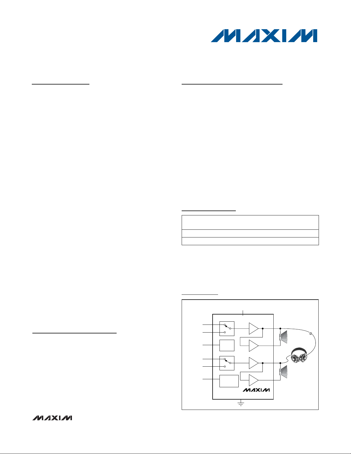
The MAX9777/MAX9778 combine a stereo 3W bridgetied load (BTL) audio power amplifier, stereo singleended (SE) headphone amplifier, headphone sensing,
and a 2:1 input multiplexer all in a tiny 28-pin thin QFN
package. These devices operate from a single 4.5V to
5.5V supply and feature an industry-leading 100dB
PSRR, allowing these devices to operate from noisy
supplies without the addition of a linear regulator. An
ultra-low 0.002% THD+N ensures clean, low-distortion
amplification of the audio signal. Click-and-pop suppression minimizes audible transients on power and
shutdown cycles. Power-saving features include low
4mV V
OS
(minimizes DC current drain through the
speakers), low 13mA supply current, and a 10µA shutdown mode. A MUTE function allows the outputs to be
quickly enabled or disabled.
A headphone sense input detects the presence of a
headphone jack and automatically configures the
amplifiers for either speaker or headphone mode. In
speaker mode, the amplifiers can deliver up to 3W of
continuous average power into a 3Ω load. In headphone mode, the amplifier can deliver up to 200mW of
continuous average power into a 16Ω load. The gain of
the amplifiers is externally set, allowing maximum flexibility in optimizing output levels for a given load. The
amplifiers also feature a 2:1 input multiplexer, allowing
multiple audio sources to be selected. The multiplexer
can also be used to compensate for limitations in the
frequency response of the loud speakers by selecting
an external equalizer network. The various functions are
controlled by either an I2C-compatible (MAX9777) or
simple parallel control interface (MAX9778).
The MAX9777/MAX9778 are available in a thermally
efficient 28-pin thin QFN package (5mm x 5mm x
0.8mm). These devices have thermal-overload protection (OVP) and are specified over the extended -40°C
to +85°C temperature range.
Features
♦ Industry-Leading, Ultra-High 100dB PSRR
♦ 3W BTL Stereo Speaker Amplifier
♦ 200mW Stereo Headphone Amplifier
♦ Low 0.002% THD+N
♦ Click-and-Pop Suppression
♦ ESD-Protected Outputs
♦ Low Quiescent Current: 13mA
♦ Low-Power Shutdown Mode: 10µA
♦ MUTE Function
♦ Headphone Sense Input
♦ Stereo 2:1 Input Multiplexer
♦ Optional 2-Wire, I
2
C-Compatible or Parallel
Interface
♦ Tiny 28-Pin Thin QFN (5mm
x 5mm x 0.8mm)
Package
MAX9777/MAX9778
Stereo 3W Audio Power Amplifiers with
Headphone Drive and Input Mux
________________________________________________________________
Maxim Integrated Products
1
SE/
BTL
SINGLE SUPPLY
4.5V TO 5.5V
I
2
C-
COMPATIBLE
MAX9777
LEFT IN1
LEFT IN2
RIGHT IN1
RIGHT IN2
CONTROL
Simplified Block Diagram
Ordering Information
19-0509; Rev 0; 4/06
For pricing, delivery, and ordering information, please contact Maxim/Dallas Direct! at
1-888-629-4642, or visit Maxim’s website at www.maxim-ic.com.
µ
PART
CONTROL
INTERFACE
PINPACKAGE
PK G
C O D E
MAX9777ETI+
T2855-6
MAX9778ETI+
Parallel
T2855-6
Pin Configurations and Functional Diagrams appear at end
of data sheet.
Note: All devices are specified over the -40°C to +85°C operating temperature range.
+Denotes lead-free package.
*EP = Exposed paddle.
Notebooks
Portable DVD Players
Tablet PCs
PC Audio Peripherals
Camcorders
Multimedia Monitor
Applications
I2C Compatible 28 Thi n QFN - E P *
28 Thi n QFN - E P *
Page 2
MAX9777/MAX9778
Stereo 3W Audio Power Amplifiers with
Headphone Drive and Input Mux
2
______________________________________________________________________________________________________________________________________________________________________________
AABBSSOOLLUUTTEE MMAAXXIIMMUUMM RRAATTIINNGGSS
Stresses beyond those listed under “Absolute Maximum Ratings” may cause permanent damage to the device. These are stress ratings only, and functional
operation of the device at these or any other conditions beyond those indicated in the operational sections of the specifications is not implied. Exposure to
absolute maximum rating conditions for extended periods may affect device reliability.
VDDto GND ...........................................................................+6V
PV
DD
to VDD.......................................................................±0.3V
PGND to GND.....................................................................±0.3V
All Other Pins to GND.................................-0.3V to (V
DD
+ 0.3V)
Continuous Input Current (into any pin except power-supply
and output pins) ...............................................................±20mA
OUT__ Short Circuit to GND, V
DD
..........................................10s
Short Circuit Between OUT_+ and OUT_- .................Continuous
Continuous Power Dissipation (T
A
= +70°C)
28-Pin TQFN, Multilayer Board
(derate 34.5mW/°C above +70°C)..........................2758.6mW
Operating Temperature Range ...........................-40°C to +85°C
Storage Temperature Range .............................-65°C to +150°C
Junction Temperature......................................................+150°C
Lead Temperature (soldering, 10s) .................................+300°C
ELECTRICAL CHARACTERISTICS
(VDD= PVDD= 5.0V, GND = PGND = 0V, V
SHDN
= 5V, C
BIAS
= 1µF, RIN= RF= 15kΩ, RL= ∞. TA= T
MIN
to T
MAX
, unless otherwise
noted. Typical values are at T
A
= +25°C.) (Note 1)
Supply Voltage Range VDD/PVDDInferred from PSRR test 4.5 5.5 V
Quiescent Supply Current
(I
Shutdown Current I
Switching Time t
Turn-On Time t
PARAMETER SYMBOL CONDITIONS MIN TYP MAX UNITS
VDD
+ I
PVDD
)
I
DD
SHDN
SW
ON
Thermal Shutdown Threshold +160
Thermal Shutdown Hysteresis 15
OUTPUT AMPLIFIERS (SPEAKER MODE, HPS = GND)
Output Offset Voltage V
Power-Supply Rejection Ratio
(Note 2)
Total Harmonic Distortion Plus
Noise
OS
PSRR
OUT
THD+N
Signal-to-Noise Ratio SNR RL = 8Ω, P
Slew Rate SR 1.6 V/µs
Maximum Capacitive Load Drive C
L
Crosstalk fIN = 10kHz 73 dB
Click/Pop Level K
CP
BTL mode, HPS = 0V, MAX9777/MAX9778 13 32
Single-ended mode, HPS = V
DD
SHDN = GND 10 50 µA
Gain or input switching 10 µs
C
= 1µF 300
BIAS
C
= 0.1µF 30
BIAS
OUT_+ - OUT_-, AV = 1V/V ±4 ±32 mV
VDD = 4.5V to 5.5V 75 100
f = 1kHz, V
f = 20kHz, V
fIN = 1kHz,
THD+N < 1%,
T
= +25°C
A
f
= 1kHz, BW =
IN
22Hz to 22kHz
= 200mV
RIPPLE
RIPPLE
= 200mV
P-P
P-P
RL = 8Ω 1.4
RL = 4Ω 2.6Output Power P
R
= 3Ω 3
L
P
= 1W, RL = 8Ω 0.005
OUT
P
= 2W, RL = 4Ω 0.01
OUT
= 1W, BW = 22Hz to 22kHz 95 dB
OUT
No sustained oscillations 1 nF
Peak voltage, A-weighted,
Into shutdown -50
32 samples per second
(Notes 2, 6)
Out of shutdown -65
718
82
70
mA
ms
o
C
o
C
dB
W
%
dBV
Page 3
MAX9777/MAX9778
Stereo 3W Audio Power Amplifiers with
Headphone Drive and Input Mux
______________________________________________________________________________________________________________________________________________________________________________
3
ELECTRICAL CHARACTERISTICS (continued)
(VDD= PVDD= 5.0V, GND = PGND = 0V, V
SHDN
= 5V, C
BIAS
= 1µF, RIN= RF= 15kΩ, RL= ∞. TA= T
MIN
to T
MAX
, unless otherwise
noted. Typical values are at T
A
= +25°C.) (Note 1)
OUTPUT AMPLIFIERS (HEADPHONE MODE, HPS = VDD)
Power-Supply Rejection Ratio
(Note 2)
Output Power P
Total Harmonic Distortion Plus
Noise
Signal-to-Noise Ratio SNR
Slew Rate SR 1.8 V/µs
Maximum Capacitive Load Drive C
Crosstalk fIN = 10kHz 78 dB
BIAS VOLTAGE (BIAS)
BIAS Voltage V
Output Resistance R
DIGITAL INPUTS (MUTE, SHDN, HPS_EN, GAINA/B, IN1111/2)
Input-Voltage High V
Input-Voltage Low V
Input Leakage Current I
HEADPHONE SENSE INPUT (HPS)
Input-Voltage High V
Input-Voltage Low V
Input Leakage Current I
Click/Pop Level K
PARAMETER SYMBOL CONDITIONS MIN TYP MAX UNITS
PSRR
OUT
THD+N
L
BIAS
BIAS
IH
IL
IN
IH
IL
IN
CP
VDD = 4.5V to 5.5V 75 106
f = 1kHz, V
f = 20kHz, V
fIN = 1kHz, THD+N <
1%, T
A
fIN = 1kHz,
BW = 22Hz to 22kHz
R
= 32Ω, BW = 22Hz to 22kHz,
L
= 1V
V
OUT
No sustained oscillations 2 nF
Peak voltage, A-weighted,
32 samples per second
(Notes 2, 4)
= 200mV
RIPPLE
RIPPLE
= +25°C
RMS
= 200mV
P-P
P-P
RL = 32Ω 88
R
= 16Ω 200
L
P
= 60mW,
OUT
= 32Ω
R
L
P
= 125mW,
OUT
= 16Ω
R
L
Into shutdown -70
Out of shutdown -52
0.002
0.002
2.35 2.5 2.65 V
2V
0.9 x
V
DD
88
76
92 dB
50 kΩ
0.8 V
±1µA
0.7 x
V
DD
±1µA
dB
mW
%
V
V
dBV
Page 4
MAX9777/MAX9778
Stereo 3W Audio Power Amplifiers with
Headphone Drive and Input Mux
4
______________________________________________________________________________________________________________________________________________________________________________
ELECTRICAL CHARACTERISTICS (continued)
(VDD= PVDD= 5.0V, GND = PGND = 0V, V
SHDN
= 5V, C
BIAS
= 1µF, RIN= RF= 15kΩ, RL= ∞. TA= T
MIN
to T
MAX
, unless otherwise
noted. Typical values are at T
A
= +25°C.) (Note 1)
Note 1: All devices are 100% production tested at +25°C. All temperature limits are guaranteed by design.
Note 2: Inputs AC-coupled to GND.
Note 3: A master device must provide a hold time of at least 300ns for the SDA signal to bridge the undefined region of SCL’s
falling edge.
Note 4: C
B
= total capacitance of one of the bus lines in picofarads. Device tested with CB= 400pF. 1kΩ pullup resistors connected
from SDA/SCL to V
DD
.
Note 5: Input filters on SDA, SCL, and ADD suppress noise spikes of less than 50ns.
Note 6: Headphone mode testing performed with 32Ω resistive load connected to GND. Speaker mode testing performed with 8Ω
resistive load connected to GND. Mode transitions are controlled by SHDN. KCP level is calculated as 20log[(peak voltage
during mode transition, no input signal)/1V
RMS
]. Units are expressed in dBV.
2-WIRE SERIAL INTERFACE (SCL, SDA, ADD, INT) (MAX9777)
Input-Voltage High V
Input-Voltage Low V
Input Hysteresis 0.2 V
Input High Leakage Current I
Input Low Leakage Current I
Input Capacitance C
Output-Voltage Low V
Output Current High I
TIMING CHARACTERISTICS (MAX9777)
Serial Clock Frequency f
Bus Free Time Between STOP
and START Conditions
START Condition Hold Time t
START Condition Setup Time t
Clock Period Low t
Clock Period High t
Data Setup Time t
Data Hold Time t
Receive SCL/SDA Rise Time t
Receive SCL/SDA Fall Time t
Transmit SDA Fall Time t
Pulse Width of Suppressed
Spike
PARAMETER SYMBOL CONDITIONS MIN TYP MAX UNITS
IH
IL
IH
IL
IN
OL
OH
SCL
t
BUF
HD:STA
SU:STA
LOW
HIGH
SU:DAT
HD:DAT
r
f
f
t
SP
VIN = 5V ±1µA
VIN = 0V ±1µA
IOL = 3mA 0.4 V
VOH = 5V 1 µA
(Note 3) 0 0.9 µs
(Note 4)
(Note 4)
(Note 4)
(Note 5) 50 ns
2.6 V
1.3 µs
0.6 µs
0.6 µs
1.3 µs
0.6 µs
100 ns
20 +
0.1C
B
20 +
0.1C
B
20 +
0.1C
B
10 pF
0.8 V
400 kHz
300 ns
300 ns
250 ns
Page 5
MAX9777/MAX9778
Stereo 3W Audio Power Amplifiers with
Headphone Drive and Input Mux
_______________________________________________________________________________________
5
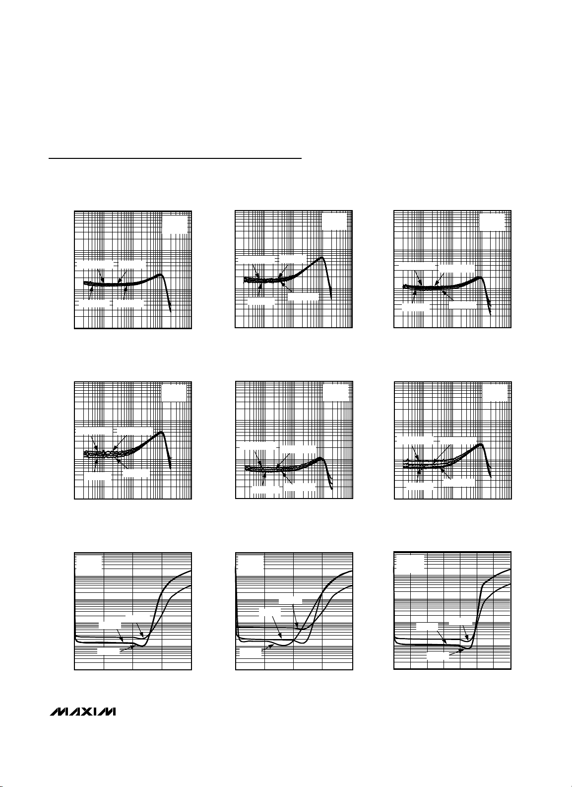
Typical Operating Characteristics
(VDD= PVDD= 5V, GND = PGND = 0V, V
SHDN
= 5V, C
BIAS
= 1µF, TA = +25°C, unless otherwise noted.)
TOTAL HARMONIC DISTORTION PLUS NOISE
vs. FREQUENCY (SPEAKER MODE)
1
0.1
P
P
= 500mW
OUT
THD+N (%)
0.01
= 2W
OUT
0.001
10 100k
= 1W
OUT
P
= 2.5WP
OUT
FREQUENCY (Hz)
10k1k100
RL = 3
= 2V/V
A
V
Ω
TOTAL HARMONIC DISTORTION PLUS NOISE
vs. FREQUENCY (SPEAKER MODE)
1
0.1
P
= 250mW
P
OUT
THD+N (%)
0.01
P
= 1W
OUT
0.001
10 100k
= 500mW
OUT
P
OUT
FREQUENCY (Hz)
= 2W
RL = 4Ω
A
10k1k100
= 4V/V
V
MAX9777/78 toc01
MAX9777/78 toc04
TOTAL HARMONIC DISTORTION PLUS NOISE
1
0.1
THD+N (%)
0.01
0.001
10 100k
TOTAL HARMONIC DISTORTION PLUS NOISE
1
0.1
THD+N (%)
0.01
0.001
10 100k
vs. FREQUENCY (SPEAKER MODE)
RL = 3Ω
A
P
P
OUT
= 500mW
P
= 2W
OUT
= 1W
OUT
P
= 2.5W
OUT
FREQUENCY (Hz)
10k1k100
vs. FREQUENCY (SPEAKER MODE)
RL = 8Ω
A
P
= 250mW
OUT
P
OUT
P
OUT
P
= 1W
FREQUENCY (Hz)
= 500mW
= 1.2W
OUT
10k1k100
= 4V/V
V
= 2V/V
V
MAX9777/78 toc02
THD+N (%)
MAX9777/78 toc05
THD+N (%)
TOTAL HARMONIC DISTORTION PLUS NOISE
vs. FREQUENCY (SPEAKER MODE)
1
0.1
P
= 250mW
OUT
0.01
P
OUT
0.001
10 100k
= 1W
P
OUT
P
FREQUENCY (Hz)
= 500mW
= 2W
OUT
RL = 4Ω
A
V
10k1k100
TOTAL HARMONIC DISTORTION PLUS NOISE
vs. FREQUENCY (SPEAKER MODE)
1
0.1
P
= 250mW
OUT
0.01
P
OUT
0.001
10 100k
= 1W
FREQUENCY (Hz)
P
OUT
P
OUT
= 500mW
= 1.2W
10k1k100
RL = 8Ω
A
= 2V/V
= 4V/V
V
MAX9777/78 toc03
MAX9777/78 toc06
TOTAL HARMONIC DISTORTION PLUS NOISE
vs. OUTPUT POWER (SPEAKER MODE)
100
AV = 2V/V
= 3Ω
R
L
10
1
THD+N (%)
0.1
0.01
0.001
04
f = 10kHz
f = 20Hz
f = 1kHz
OUTPUT POWER (W)
321
MAX9777/78 toc07
TOTAL HARMONIC DISTORTION PLUS NOISE
vs. OUTPUT POWER (SPEAKER MODE)
100
AV = 4V/V
= 3Ω
R
L
10
1
THD+N (%)
0.1
0.01
0.001
f = 1kHz
f = 20Hz
04
f = 10kHz
OUTPUT POWER (W)
TOTAL HARMONIC DISTORTION PLUS NOISE
vs. OUTPUT POWER (SPEAKER MODE)
100
AV = 2V/V
= 4Ω
R
L
10
MAX9777/78 toc08
1
THD+N (%)
0.1
0.01
0.001
321
f = 1kHz
0 3.5
f = 10kHz
f = 20Hz
2.5 3.02.01.51.00.5
OUTPUT POWER (W)
MAX9777/78 toc09
Page 6
MAX9777/MAX9778
Stereo 3W Audio Power Amplifiers with
Headphone Drive and Input Mux
6
______________________________________________________________________________________________________________________________________________________________________________
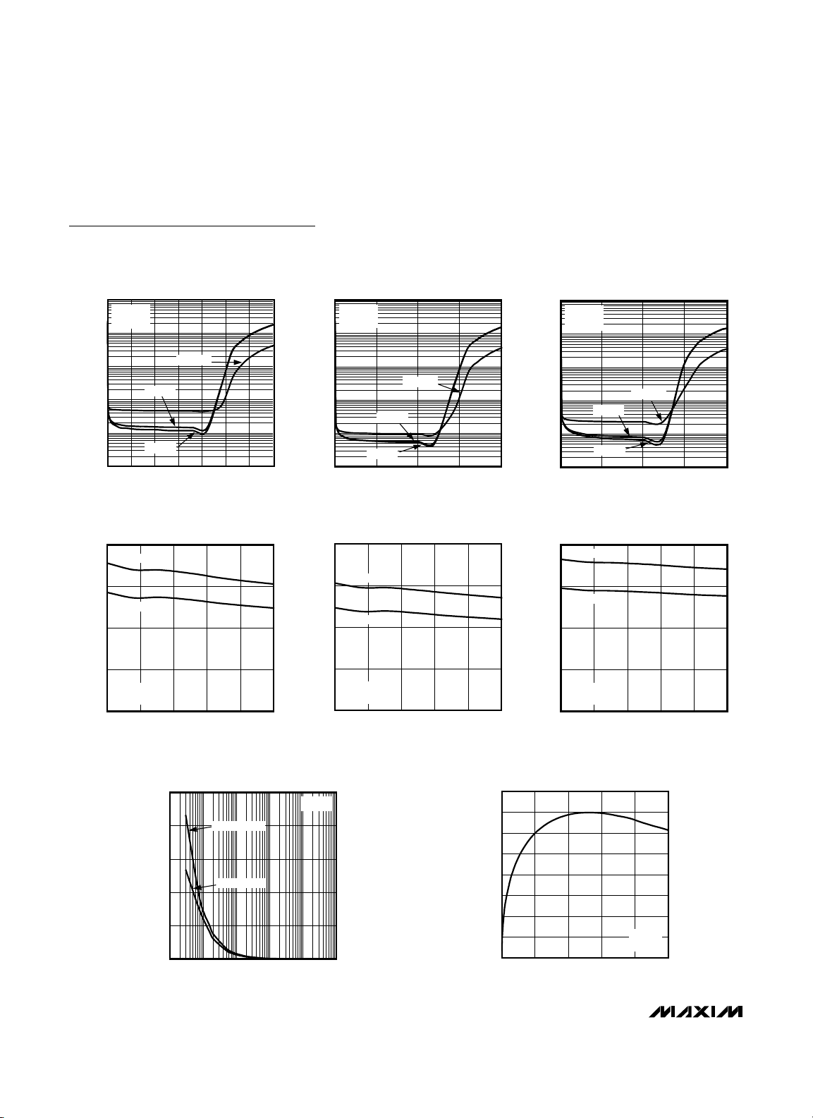
Typical Operating Characteristics (continued)
(VDD= PVDD= 5V, GND = PGND = 0V, V
SHDN
= 5V, C
BIAS
= 1µF, TA = +25°C, unless otherwise noted.)
TOTAL HARMONIC DISTORTION PLUS NOISE
vs. OUTPUT POWER (SPEAKER MODE)
100
AV = 4V/V
= 4Ω
R
L
10
1
THD+N (%)
0.1
0.01
0.001
0 3.5
OUTPUT POWER vs. AMBIENT TEMPERATURE
f = 10kHz
f = 1kHz
f = 20Hz
2.5 3.02.01.51.00.5
OUTPUT POWER (W)
(SPEAKER MODE)
4
THD+N = 10%
3
THD+N = 1%
2
TOTAL HARMONIC DISTORTION PLUS NOISE
vs. OUTPUT POWER (SPEAKER MODE)
100
AV = 2V/V
= 8Ω
R
L
10
MAX9777/78 toc10
1
f = 10kHz
THD+N (%)
0.1
f = 1kHz
0.01
0.001
f = 20Hz
0 2.0
OUTPUT POWER (W)
OUTPUT POWER vs. AMBIENT TEMPERATURE
(SPEAKER MODE)
4
MAX9777/78 toc13
3
2
THD+N = 10%
THD+N = 1%
TOTAL HARMONIC DISTORTION PLUS NOISE
vs. OUTPUT POWER (SPEAKER MODE)
100
AV = 4V/V
= 8Ω
R
L
10
MAX9777/78 toc11
1
THD+N (%)
0.1
0.01
1.51.00.5
0.001
0 2.0
OUTPUT POWER vs. AMBIENT TEMPERATURE
2.0
THD+N = 10%
MAX9777/78 toc14
1.5
THD+N = 1%
1.0
MAX9777/78 toc12
f = 10kHz
f = 1kHz
f = 20Hz
1.51.00.5
OUTPUT POWER (W)
(SPEAKER MODE)
MAX9777/78 toc15
OUTPUT POWER (W)
1
f = 1kHz
= 3Ω
R
L
0
-40 85
AMBIENT TEMPERATURE (°C)
603510-15
OUTPUT POWER (W)
1
f = 1kHz
= 4Ω
R
L
0
-40 85
AMBIENT TEMPERATURE (°C)
603510-15
OUTPUT POWER vs. LOAD RESISTANCE
(SPEAKER MODE)
5
4
3
2
OUTPUT POWER (W)
1
0
1 100k
THD+N = 10%
THD+N = 1%
LOAD RESISTANCE (Ω)
f = 1kHz
MAX9777/78 toc16
10k1k10010
1.6
1.4
1.2
1.0
0.8
0.6
POWER DISSIPATION (W)
0.4
0.2
0
OUTPUT POWER (W)
0.5
f = 1kHz
= 8Ω
R
L
0
-40 85
POWER DISSIPATION vs. OUTPUT POWER
(SPEAKER MODE)
0
OUTPUT POWER (W)
AMBIENT TEMPERATURE (°C)
MAX9777/78 toc17
RL = 4Ω
f = 1kHz
2.50.5 1.0 1.5 2.0
603510-15
Page 7
MAX9777/MAX9778
Stereo 3W Audio Power Amplifiers with
Headphone Drive and Input Mux
_______________________________________________________________________________________
7
Typical Operating Characteristics (continued)
(VDD= PVDD= 5V, GND = PGND = 0V, V
SHDN
= 5V, C
BIAS
= 1µF, TA = +25°C, unless otherwise noted.)
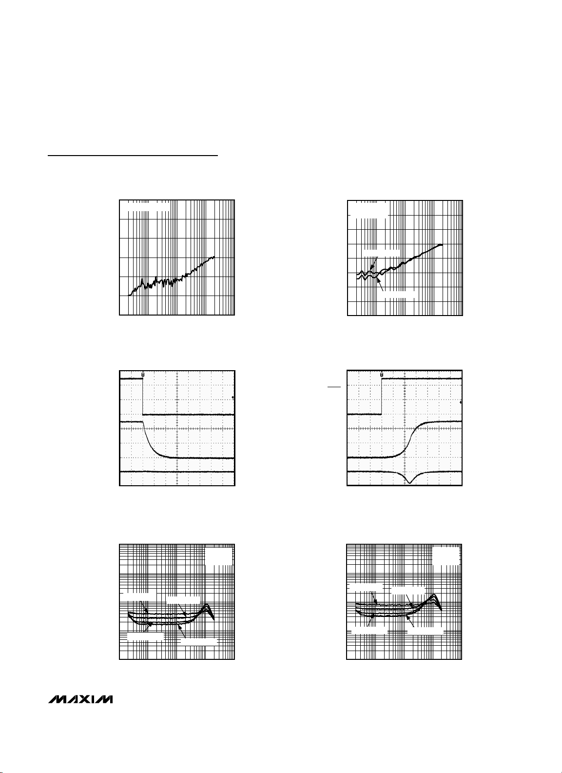
POWER-SUPPLY REJECTION RATIO
vs. FREQUENCY (SPEAKER MODE)
40
V
= 200mV
RIPPLE
50
60
70
PSRR (dB)
80
90
100
10 100k
P-P
FREQUENCY (Hz)
ENTERING SHUTDOWN (SPEAKER MODE)
V
DD
2V/div
OUT_+ AND OUT_-
1V/div
10k1k100
MAX9777/78 toc20
MAX9777/78 toc18
CROSSTALK (dB)
-100
-110
-120
SHDN
2V/div
OUT_+ AND OUT_-
1V/div
CROSSTALK vs. FREQUENCY
(SPEAKER MODE)
-40
VIN = 200mV
P-P
RL = 8Ω
-50
-60
-70
-80
-90
RIGHT TO LEFT
LEFT TO RIGHT
10 100k
FREQUENCY (Hz)
EXITING SHUTDOWN (SPEAKER MODE)
10k1k100
MAX9777/78 toc21
MAX9777/78 toc19
OUT_+ - OUT_-
200mV/div
0.1
0.01
THD+N (%)
0.001
0.0001
OUT_+ - OUT_-
500mV/div
400ms/div
TOTAL HARMONIC DISTORTION PLUS NOISE
vs. FREQUENCY (HEADPHONE MODE)
1
P
= 25mW
OUT
P
OUT
10 100k
= 100mW
P
OUT
FREQUENCY (Hz)
= 50mW
P
OUT
RL = 16Ω
A
= 150mW
10k1k100
= 1V/V
V
MAX9777/78 toc22
TOTAL HARMONIC DISTORTION PLUS NOISE
vs. FREQUENCY (HEADPHONE MODE)
1
0.1
P
= 25mW
OUT
0.01
THD+N (%)
P
0.001
0.0001
= 100mW
OUT
10 100k
100ms/div
P
= 50mW
OUT
P
OUT
FREQUENCY (Hz)
RL = 16Ω
A
= 150mW
10k1k100
= 2V/V
V
MAX9777/78 toc23
Page 8
MAX9777/MAX9778
Stereo 3W Audio Power Amplifiers with
Headphone Drive and Input Mux
8
______________________________________________________________________________________________________________________________________________________________________________
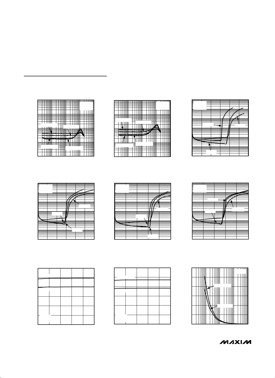
E
Typical Operating Characteristics (continued)
(VDD= PVDD= 5V, GND = PGND = 0V, V
SHDN
= 5V, C
BIAS
= 1µF, TA = +25°C, unless otherwise noted.)
TOTAL HARMONIC DISTORTION PLUS NOISE
vs. FREQUENCY (HEADPHONE MODE)
MAX9777/78 toc25
FREQUENCY (Hz)
THD+N (%)
10k1k100
0.001
0.01
0.1
1
0.0001
10 100k
RL = 32Ω
A
V
= 2V/V
P
OUT
= 50mW
P
OUT
= 25mW
P
OUT
= 100mW
P
OUT
= 150mW
TOTAL HARMONIC DISTORTION PLUS NOISE
vs. OUTPUT POWER (HEADPHONE MODE)
MAX9777/78 toc26
OUTPUT POWER (mW)
THD+N (%)
25020015010050
0.01
0.001
10
1
0.1
100
0.0001
0 300
AV = 1V/V
R
L
= 16Ω
f = 20Hz
f = 1kHz
f = 10kHz
TOTAL HARMONIC DISTORTION PLUS NOISE
vs. OUTPUT POWER (HEADPHONE MODE)
MAX9777/78 toc27
OUTPUT POWER (mW)
THD+N (%)
25020015010050
0.01
0.001
10
1
0.1
100
0.0001
0 300
AV = 2V/V
R
L
= 16Ω
f = 20Hz
f = 1kHz
f = 10kHz
TOTAL HARMONIC DISTORTION PLUS NOISE
vs. FREQUENCY (HEADPHONE MODE)
MAX9777/78 toc24
FREQUENCY (Hz)
THD+N (%)
10k1k100
0.001
0.01
0.1
1
0.0001
10 100k
RL = 32Ω
A
V
= 1V/V
P
OUT
= 50mW
P
OUT
= 25mW
P
OUT
= 100mW
P
OUT
= 150mW
OUTPUT POWER vs. AMBIENT TEMPERATURE
300
250
200
150
100
OUTPUT POWER (mW)
50
0
-40 85
(HEADPHONE MODE)
THD+N = 10%
THD+N = 1%
f = 1kHz
= 16Ω
R
L
AMBIENT TEMPERATURE (°C)
603510-15
TOTAL HARMONIC DISTORTION PLUS NOISE
vs. OUTPUT POWER (HEADPHONE MODE)
100
AV = 1V/V
= 32Ω
R
L
10
1
0.1
THD+N (%)
0.01
0.001
0.0001
0 125
f = 20Hz
OUTPUT POWER (mW)
OUTPUT POWER vs. AMBIENT TEMPERATUR
(HEADPHONE MODE)
150
THD+N = 10%
125
MAX9777/78 toc30
100
THD+N = 1%
75
50
OUTPUT POWER (mW)
25
f = 1kHz
= 32Ω
R
L
0
-40 85
AMBIENT TEMPERATURE (°C)
f = 1kHz
f = 10kHz
100755025
603510-15
100
MAX9777/78 toc28
THD+N (%)
0.01
0.001
0.0001
600
500
MAX9777/78 toc331
400
300
200
OUTPUT POWER (mW)
100
TOTAL HARMONIC DISTORTION PLUS NOISE
vs. OUTPUT POWER (HEADPHONE MODE)
AV = 2V/V
= 32Ω
R
L
10
1
0.1
0 125
f = 1kHz
f = 20Hz
OUTPUT POWER (mW)
f = 10kHz
100755025
OUTPUT POWER vs. LOAD RESISTANCE
(HEADPHONE MODE)
f = 1kHz
THD+N = 10%
THD+N = 1%
0
1 10k
LOAD RESISTANCE (Ω)
1k10010
MAX9777/78 toc29
MAX9777/78 toc32
Page 9
MAX9777/MAX9778
Stereo 3W Audio Power Amplifiers with
Headphone Drive and Input Mux
_______________________________________________________________________________________
9
Typical Operating Characteristics (continued)
(VDD= PVDD= 5V, GND = PGND = 0V, V
SHDN
= 5V, C
BIAS
= 1µF, TA = +25°C, unless otherwise noted.)
POWER-SUPPLY REJECTION RATIO
vs. FREQUENCY (HEADPHONE MODE)
MAX9777/78 toc35
FREQUENCY (Hz)
PSRR (dB)
10k1k100
90
80
70
60
50
40
100
10 100k
V
RIPPLE
= 200mV
P-P
CROSSTALK vs. FREQUENCY
(HEADPHONE MODE)
MAX9777/78 toc36
FREQUENCY (Hz)
CROSSTALK (dB)
10k1k100
-110
-100
-90
-80
-70
-60
-50
-40
-120
10 100k
VIN = 200mV
P-P
RL = 16Ω
RIGHT TO LEFT
LEFT TO RIGHT
POWER DISSIPATION vs. OUTPUT POWER
(HEADPHONE MODE)
MAX9777/78 toc33
OUTPUT POWER (mW)
POWER DISSIPATION (mW)
50 100 150 200
20
40
60
80
100
120
0
0
RL = 16Ω
f = 1kHz
POWER DISSIPATION vs. OUTPUT POWER
(HEADPHONE MODE)
MAX9777/78 toc34
OUTPUT POWER (mW)
POWER DISSIPATION (mW)
10020 40 60 80
10
20
30
40
50
60
70
0
0
RL = 32Ω
f = 1kHz
EXITING SHUTDOWN (HEADPHONE MODE)
SHDN
2V/div
OUT_+
1V/div
MAX9777/78 toc37
SHDN
2V/div
OUT_+
1V/div
HP JACK
100mV/div
HP JACK
200mV/div
RL = 16Ω
INPUT AC-COUPLED TO GND
100ms/div
SUPPLY CURRENT vs. SUPPLY VOLTAGE
ENTERING SHUTDOWN (HEADPHONE MODE)
100ms/div
MAX9777/78 toc38
25
20
15
10
SUPPLY CURRENT (mA)
5
0
4.50 5.50
(SPEAKER MODE)
TA = +85°C
MAX9777/78 toc39
TA = +25°C
TA = -40°C
5.255.004.75
SUPPLY VOLTAGE (V)
Page 10

MAX9777/MAX9778
Stereo 3W Audio Power Amplifiers with
Headphone Drive and Input Mux
10
____________________________________________________________________________________________________________________________________________________________________________
Typical Operating Characteristics (continued)
(VDD= PVDD= 5V, GND = PGND = 0V, V
SHDN
= 5V, C
BIAS
= 1µF, TA = +25°C, unless otherwise noted.)
SUPPLY CURRENT vs. SUPPLY VOLTAGE
(HEADPHONE MODE)
MAX9777/78 toc40
SUPPLY VOLTAGE (V)
SUPPLY CURRENT (mA)
5.255.004.75
2
4
6
8
10
12
0
4.50 5.50
TA = +85°C
TA = +25°C
TA = -40°C
POWER DISSIPATION vs. OUTPUT POWER
(SPEAKER MODE)
MAX9777/78 toc42
OUTPUT POWER (W)
POWER DISSIPATION (W)
1.500.25 0.50 0.75 1.00 1.25
0.1
0.2
0.3
0.4
0.5
0.6
0.7
0.8
0
0
RL = 8Ω
f = 1kHz
EXITING POWER-DOWN
(SPEAKER MODE)
MAX9777/78 toc43
100ms/div
OUT_+ AND OUT_-
1V/div
OUT_+ - OUT_-
1V/div
V
DD
2V/div
SUPPLY CURRENT vs. SUPPLY VOLTAGE
(HEADPHONE MODE)
MAX9777/78 toc40
SUPPLY VOLTAGE (V)
SUPPLY CURRENT (mA)
5.255.004.75
2
4
6
8
10
12
0
4.50 5.50
TA = +85°C
TA = +25°C
TA = -40°C
Page 11

MAX9777/MAX9778
Stereo 3W Audio Power Amplifiers with
Headphone Drive and Input Mux
____________________________________________________________________________________________________________________________________________________________________________
11
Pin Description
PIN
MAX9777 MAX9778
1 — SDA Serial Data I/O
2—INT Interrupt Output
3, 4 3, 4 V
5 5 INL1 Left-Channel Input 1
6 6 INL2 Left-Channel Input 2
7 7 GAINLA Left-Channel Gain Set A
8 8 GAINLB Left-Channel Gain Set B
9, 13, 23, 27 9, 13, 23, 27 PGND Power Ground. Connect to GND.
10 10 OUTL+
11, 25 11, 25 PV
12 12 OUTL- Left-Channel Bridged Amplifier Negative Output
14 14 SHDN Active-Low Shutdown Input. Connect SHDN to VDD for normal operation.
15 — ADD
16 16 HPS
17 17 BIAS
18 18 GND Ground. Connect to PGND.
19 19 INR1 Right-Channel Input 1
20 20 INR2 Right-Channel Input 2
21 21 GAINRA Right-Channel Gain Set A
22 22 GAINRB Right-Channel Gain Set B
24 24 OUTR+
26 26 OUTR- Right-Channel Bridged Amplifier Negative Output
28 — SCL Serial Clock Line
— 1 MUTE Active-High Mute Input
— 2 HPS_EN
— 15 GAINA/B
—28IN1/2
EP EP EP Exposed Paddle. Connect to GND.
NAME FUNCTION
DD
DD
Power-Supply Input
Left-Channel Bridged Amplifier Positive Output. OUTL+ also serves as the
left-channel headphone amplifier output.
Output Amplifier Power Supply
Address Select. A logic-high sets the address LSB to 1, a logic-low sets the
address LSB to zero.
Headphone Sense Input. A logic-high configures the device as a singleended headphone amp. A logic-low configures the device as a BTL
speaker amp.
DC Bias Bypass Terminal. See the BIAS Capacitor section for capacitor
selection. Connect C
Right-Channel Bridged Amplifier Positive Output. OUTR+ also serves as the
right-channel headphone amplifier output.
Headphone Enable. A logic-high enables HPS. A logic-low disables HPS
and the device is always configured as a BTL speaker amplifier.
Gain Select. A logic-low selects the gain set by GAIN_A. A logic-high
selects the gain set by GAIN_B.
Input Select. A logic-low selects amplifier input 1. A logic-high selects
amplifier input 2.
from BIAS to GND.
BIAS
Page 12

MAX9777/MAX9778
Stereo 3W Audio Power Amplifiers with
Headphone Drive and Input Mux
12
____________________________________________________________________________________________________________________________________________________________________________
Detailed Description
The MAX9777/MAX9778 feature 3W BTL speaker
amplifiers, 200mW headphone amplifiers, input multiplexers, headphone sensing, and comprehensive clickand-pop suppression. The MAX9777/MAX9778 are
stereo BTL/headphone amplifiers. The MAX9777 is
controlled through an I2C-compatible, 2-wire serial
interface. The MAX9778 is controlled through five logic
inputs: MUTE, SHDN, HPS_EN, GAINA/B, and IN1/2
(see the
Selector Guide
). The MAX9777/MAX97778 feature exceptional PSRR (100dB at 1kHz), allowing these
devices to operate from noisy digital supplies without
the need for a linear regulator.
The speaker amplifiers use a BTL configuration. The
signal path is composed of an input amplifier and an
output amplifier. Resistor RINsets the input amplifier’s
gain, and resistor RFsets the output amplifier’s gain.
The output of these two amplifiers serves as the input to
a slave amplifier configured as an inverting unity-gain
follower. This results in two outputs, identical in magnitude, but 180°out of phase. The overall gain of the
speaker amplifiers is twice the product of the two
amplifier gains (see the
Gain-Setting Resistors
section).
A feature of this architecture is that there is no phase
inversion from input to output.
When configured as a headphone (single-ended) amplifier, the slave amplifier is disabled, muting the speaker
and the main amplifier drives the headphone. The
MAX9777/MAX9778 can deliver 3W of continuous power
into a 3Ω load with less than 1% THD+N in speaker
mode, and 200mW of continuous average power into a
16Ω load with less than 1% THD+N in headphone mode.
These devices also feature thermal-overload protection.
BIAS
These devices operate from a single 5V supply, and feature an internally generated, power-supply independent,
common-mode bias voltage of 2.5V referenced to GND.
BIAS provides both click-and-pop suppression and sets
the DC bias level for the audio outputs. BIAS is internally
connected to the noninverting input of each speaker
amplifier (see the
Typical Application Circuits
and
Functional Diagrams
). Choose the value of the bypass
capacitor as described in the
BIAS Capacitor
section.
No external load should be applied to BIAS. Any load
lowers the BIAS voltage, affecting the overall performance of the device.
Input Multiplexer
Each amplifier features a 2:1 input multiplexer, allowing
input selection between two stereo sources. Both multiplexers are controlled by bit 1 in the control register
(MAX9777) or by the IN1/2 pin (MAX9778). A logic-low
selects input IN_1 and a logic-high selects input IN_2.
The input multiplexer can also be used to further
expand the number of gain options available from the
MAX9777/MAX9778 family. Connecting the audio
source to the device through two different input resistors (Figure 1) increases the number of gain options
from two to four. Additionally, the input multiplexer
allows a speaker equalization network to be switched
into the speaker signal path. This is typically useful in
optimizing acoustic response from speakers with small
physical dimensions.
Headphone Sense Enable
The HPS input is enabled by HPS_EN (MAX9778) or the
HPS_D bit (MAX9777). HPS_D or HPS_EN determines
whether the device is in automatic detection mode or
fixed-mode operation (see Tables 1a and 1b).
Figure 1. Using the Input Multiplexer for Gain Setting
Table 1a. MAX9777 HPS Setting
*Note:
A—GAINA path selected
B—GAINB path selected
A or B—Gain path selected by GAINAB control bit in register
02h
MAX9777
15kΩ
AUDIO
INPUT
HPS_D
BIT
0 0 X BTL A
01X SE B
1 X 0 BTL A or B
1 X 1 SE A or B
INPUTS
HPS
30kΩ
SPKR/HP
BIT
IN_1
IN_2
MODE
MAX9778
GAIN
PATH*
Page 13

MAX9777/MAX9778
Stereo 3W Audio Power Amplifiers with
Headphone Drive and Input Mux
______________________________________________________________________________________ 13
Headphone Sense Input (HPS)
With headphone sense enabled, a voltage on HPS less
than 0.7 x V
DD
sets the device to speaker mode. A voltage greater than 0.9 x VDDdisables the inverting
bridge amplifier (OUT_-), which mutes the speaker
amplifier and sets the device into headphone mode.
For automatic headphone detection, enable headphone
sense and connect HPS to the control pin of a 3-wire
headphone jack as shown in Figure 2. With no headphone present, the resistive voltage-divider created by
R1 and R2 sets the voltage on HPS to be less than 0.7 x
V
DD
, setting the device to speaker mode and the gain
setting defaults to GAINA (MAX9777). When a headphone plug is inserted into the jack, the control pin is disconnected from the tip contact, and HPS is pulled to V
DD
through R1, setting the device into headphone mode and
the gain-setting defaults to GAINB (MAX9777) (see the
Gain Select
section). Place a resistor in series with the
control pin and HPS (R3) to prevent any audio signal from
coupling into HPS when the device is in speaker mode.
Shutdown
The MAX9777/MAX9778 feature a 10µA, low-power
shutdown mode that reduces quiescent current consumption and extends battery life. The drive amplifiers
and bias circuitry are disabled, the amplifier outputs
(OUT_) go high impedance, and BIAS is driven to
GND. Driving SHDN low places the devices into shutdown mode, disables the interface, and resets the I2C
registers to a default state. A logic-high on SHDN
enables the devices.
MAX9777 Software Shutdown
A logic-high on bit 0 of the SHDN register places the
MAX9777 in shutdown mode. A logic-low enables the
device. The digital section of the MAX9777 remains
active when the device is shut down through the interface. All devices feature a logic-low on the SHDN input.
MUTE
The MAX9777/MAX9778 feature a mute mode. When
the device is muted, the input is disconnected from the
amplifiers. MUTE does not shut down the device.
MAX9777 MUTE
The MAX9777 MUTE mode is selected by writing to the
MUTE register (see the
Mute Register
section). The left
and right channels can be independently muted.
MAX9778 MUTE
The MAX9778 features an active-high MUTE input that
mutes all channels.
Click-and-Pop Suppression
The MAX9777/MAX9778 feature Maxim’s comprehensive click-and-pop suppression. When entering or exiting shutdown, the common-mode bias voltage of the
amplifiers is slowly ramped to and from the DC bias
point using an S-shaped waveform. In headphone
mode, this waveform shapes the frequency spectrum,
minimizing the amount of audible components present
at the headphone. In speaker mode, the BTL amplifiers
start up in the same fashion as in headphone mode.
When entering shutdown, both amplifier outputs ramp
to GND quickly and simultaneously. To maximize clickand-pop suppression, drive SHDN to 0V before powerup or power-down transitions.
MAX9777
MAX9778
R3
47kΩ
R1
680kΩ
R2
10kΩR210kΩ
HPS
V
DD
OUTL+
OUTR+
Figure 2. HPS Configuration Circuit
INPUTS
HPS_EN HPS
MODE GAIN PATH*
0 X BTL A or B
1 0 BTL A or B
1 1 SE A or B
Table 1b. MAX9778 HPS Setting
*Note:
A or B—Gain path selected by external GAINAB
Page 14

MAX9777/MAX9778
Stereo 3W Audio Power Amplifiers with
Headphone Drive and Input Mux
14
____________________________________________________________________________________________________________________________________________________________________________
Digital Interface
The MAX9777 features an I2C/SMBus™-compatible 2wire serial interface consisting of a serial data line
(SDA) and a serial clock line (SCL). SDA and SCL facilitate bidirectional communication between the
MAX9777 and the master at clock rates up to 400kHz.
Figure 3 shows the 2-wire interface timing diagram. The
MAX9777 is a transmit/receive slave-only device, relying upon a master to generate a clock signal. The master (typically a microcontroller) initiates data transfer on
the bus and generates SCL to permit that transfer.
A master device communicates to the MAX9777 by
transmitting the proper address followed by a command and/or data words. Each transmit sequence is
framed by a START (S) or REPEATED START (S
r
) condition and a STOP (P) condition. Each word transmitted
over the bus is 8 bits long and is always followed by an
acknowledge clock pulse.
SDA and SCL are open-drain outputs requiring a pullup
resistor (500Ω or greater) to generate a logic-high voltage. Series resistors in line with SDA and SCL are optional. These series resistors protect the input stages of the
devices from high-voltage spikes on the bus lines, and
minimize crosstalk and undershoot of the bus signals.
Bit Transfer
One data bit is transferred during each SCL clock
cycle. The data on SDA must remain stable during the
high period of the SCL clock pulse. Changes in SDA
while SCL is high are control signals (see the
START
and STOP Conditions
section). SDA and SCL idle high
when the I2C bus is not busy.
START and STOP Conditions
When the serial interface is inactive, SDA and SCL idle
high. A master device initiates communication by issuing a START condition. A START condition is a high-tolow transition on SDA with SCL high. A STOP condition
is a low-to-high transition on SDA while SCL is high
(Figure 4). A START condition from the master signals
the beginning of a transmission to the MAX9777. The
master terminates transmission by issuing the STOP
condition; this frees the bus. If a REPEATED START
condition is generated instead of a STOP condition, the
bus remains active.
Figure 3. 2-Wire Serial-Interface Timing Diagram
Figure 4. START/STOP Conditions
SMBus is a trademark of Intel Corp.
SDA
t
SU, DAT
t
LOW
t
HD, DAT
t
t
HD, STA
t
HD, STA
t
SP
t
SU, STO
BUF
SCL
t
t
HD, STA
START
CONDITION
HIGH
t
R
SCL
SDA
t
F
REPEATED
START
CONDITION
SS
r
P
STOP
CONDITION
START
CONDITION
Page 15

MAX9777/MAX9778
Stereo 3W Audio Power Amplifiers with
Headphone Drive and Input Mux
____________________________________________________________________________________________________________________________________________________________________________
15
Early STOP Conditions
The MAX9777 recognizes a STOP condition at any
point during the transmission except if a STOP condition occurs in the same high pulse as a START condition (Figure 5). This condition is not a legal I
2
C format;
at least one clock pulse must separate any START and
STOP condition.
REPEATED START Conditions
A REPEATED START (Sr) condition may indicate a
change of data direction on the bus. Such a change
occurs when a command word is required to initiate a
read operation. Srmay also be used when the bus
master is writing to several I2C devices and does not
want to relinquish control of the bus. The MAX9777 serial interface supports continuous write operations with
or without an Srcondition separating them. Continuous
read operations require Srconditions because of the
change in direction of data flow.
Acknowledge Bit (ACK)
The acknowledge bit (ACK) is the ninth bit attached to
any 8-bit data word. The receiving device always generates ACK. The MAX9777 generates an ACK when
receiving an address or data by pulling SDA low during
the night clock period. When transmitting data, the
MAX9777 waits for the receiving device to generate an
ACK. Monitoring ACK allows for detection of unsuccessful data transfers. An unsuccessful data transfer
occurs if a receiving device is busy or if a system fault
has occurred. In the event of an unsuccessful data
transfer, the bus master should reattempt communication at a later time.
Slave Address
The bus master initiates communication with a slave
device by issuing a START condition followed by a 7-bit
slave address (Figure 6). When idle, the MAX9777
waits for a START condition followed by its slave
address. The LSB of the address word is the
Read/Write (R/W) bit. R/W indicates whether the master
is writing to or reading from the MAX9777 (R/W = 0
selects the write condition, R/W = 1 selects the read
condition). After receiving the proper address, the
MAX9777 issues an ACK by pulling SDA low for one
clock cycle.
The MAX9777 has a factory-/user-programmed
address. Address bits A6–A2 are preset, while A0 and
A1 is set by ADD. Connect ADD to either VDD, GND,
SCL, or SDA to change the last 2 bits of the slave
address (Table 2).
Figure 5. Early STOP Condition
Figure 6. Slave Address Byte Definition
Table 2. MAX9777 I2C Slave Addresses
SCL
SDA
STOP START
LEGAL STOP CONDITION
SCL
S A6A5A4A3A2A1A0R/W
SDA
START
ILLEGAL EARLY STOP CONDITION
ILLEGAL
STOP
ADD CONNECTION I2C ADDRESS
GND 100 1000
V
DD
SDA 100 1010
SCL 100 1011
100 1001
Page 16

MAX9777/MAX9778
Stereo 3W Audio Power Amplifiers with
Headphone Drive and Input Mux
16
____________________________________________________________________________________________________________________________________________________________________________
Write Data Format
There are three registers that configure the MAX9777:
the MUTE register, SHDN register, and control register.
In write data mode (R/W = 0), the register address and
data byte follow the device address (Figure 7).
MUTE Register
The MUTE register (01hex) is a read/write register that
sets the MUTE status of the device. Bit 3 (MUTEL) of
the MUTE register controls the left channel; bit 4
(MUTER) controls the right channel. A logic-high mutes
the respective channel; a logic-low brings the channel
out of mute.
SHDN Register
The SHDN register (02hex) is a read/write register that
controls the power-up state of the device. A logic-high
in bit 0 of the SHDN register shuts down the device; a
logic-low turns on the device. A logic-high is required in
bits 2 to 7 to reset all registers to their default settings.
Control Register
The control register (03hex) is a read/write register that
determines the device configuration. Bit 1 (IN1/IN2) controls the input multiplexer, a logic-high selects input 1; a
logic-low selects input 2. Bit 2 (HPS_D) controls the
headphone sensing. A logic-low configures the device in
automatic headphone detection mode. A logic-high disables the HPS input. Bit 3 (GAINA/B) controls the gainselect multiplexer. A logic-low selects GAINA. A logichigh selects GAINB. GAINA/B is ignored when HPS_D =
0. Bit 4 (SPKR/HP) selects the amplifier operating mode
when HPS_D = 1. A logic-high selects speaker mode,
and a logic-low selects headphone mode.
Figure 7. Write/Read Data Format Example
Table 3. MAX9777 MUTE Register Format
*Default state.
Table 4. MAX9777 SHDN Register Format
*Default state.
S ADDRESS
2
I
C SLAVE ADDRESS.
SELECTS DEVICE.
S ADDRESS
7 BITS 8 BITS 8 BITS 1
2
I
C SLAVE ADDRESS.
SELECTS DEVICE.
WR ACK COMMAND ACK DATA ACK P
7 BITS 8 BITS 8 BITS 1
REGISTER ADDRESS.
SELECTS REGISTER TO BE
WR ACK COMMAND ACK DATA P
REGISTER ADDRESS.
SELECTS REGISTER
WRITTEN TO.
TO BE READ.
REGISTER DATA
S ADDRESS
7 BITS
2
C SLAVE ADDRESS.
I
SELECTS DEVICE.
WR ACK
DATA FROM
SELECTED REGISTER
REGISTER
ADDRESS
BIT NAME VALUE DESCRIPTION
7 X Don’t Care —
6 X Don’t Care —
5 X Don’t Care —
4 MUTER
3 MUTEL
2 X Don’t Care —
1 X Don’t Care —
0 X Don’t Care —
0* Unmute right channel
1 Mute right channel
0* Unmute left channel
1 Mute left channel
0000 0001
REGISTER ADDRESS 0000 0010
BIT NAME VALUE DESCRIPTION
7 RESET
6 RESET
5 RESET
4 RESET
3 RESET
2 RESET
1 X Don’t Care —
0 SHDN
0* —
1 Reset device
0* —
1 Reset device
0* —
1 Reset device
0* —
1 Reset device
0* —
1 Reset device
0* —
1 Reset device
0* Normal operation
1 Shutdown
Page 17

MAX9777/MAX9778
Stereo 3W Audio Power Amplifiers with
Headphone Drive and Input Mux
____________________________________________________________________________________________________________________________________________________________________________
17
Read Data Format
In read mode (R/W = 1), the MAX9777 writes the contents of the selected register to the bus. The direction of
the data flow reverses following the address acknowledge by the MAX9777. The master device reads the
contents of all registers, including the read-only status
register. Table 6 shows the status register format.
Interrupt Output (INT)
The MAX9777 includes an interrupt output (INT) that
can indicate to a master device that an event has
occurred. INT is triggered when the state of HPS
changes. During normal operation, INT idles high. If a
headphone is inserted/removed from the jack and that
action is detected by HPS, INT pulls the line low. INT
remains low until a read data operation is executed.
I2C Compatibility
The MAX9777 is compatible with existing I2C systems.
SCL and SDA are high-impedance inputs; SDA has an
open drain that pulls the data line low during the ninth
clock pulse. The communication protocol supports the
standard I2C 8-bit communications. The general call
address is ignored. The MAX9777 slave addresses are
compatible with the 7-bit I2C addressing protocol only.
*Default
Table 5. MAX9777 Control Register Format
Table 6. MAX9777 Status Register Format
REGISTER ADDRESS 0000 0011
BIT NAME VALUE DESCRIPTION
7 X Don’t Care —
6 X Don’t Care —
5 X Don’t Care —
0* Speaker mode selected
4 SPKR/HP
3 GAINA/B
2 HPS_D
1 IN1/IN2
0 X Don’t Care —
0* Gain-setting A selected
0*
0* Input 1 selected
Headphone mode
1
selected
1 Gain-setting B selected
Automatic headphone
detection enabled
Automatic headphone
1
detection disabled
(HPS ignored)
1 Input 2 selected
REGISTER ADDRESS 0000 0000
BIT NAME VALUE DESCRIPTION
7 THRM
6 AMPR-
5 AMPR+
4 AMPL-
3 AMPL+
2 HPSTS
1 X Don’t Care —
0 X Don’t Care —
0 Device temperature below thermal limit
1 Device temperature exceeding thermal limit
0 OUTR- current below current limit
1 OUTR- current exceeding current limit
0 OUTR+ current below current limit
1 OUTR+ current exceeding current limit
0 OUTL- current below current limit
1 OUTL- current exceeding current limit
0 OUTL+ current below current limit
1 OUTL+ current exceeding current limit
0 Device in speaker mode
1 Device in headphone mode
Page 18

MAX9777/MAX9778
Stereo 3W Audio Power Amplifiers with
Headphone Drive and Input Mux
18
____________________________________________________________________________________________________________________________________________________________________________
Applications Information
BTL Speaker Amplifiers
The MAX9777/MAX9778 feature speaker amplifiers
designed to drive a load differentially, a configuration
referred to as bridge-tied load (BTL). The BTL configuration (Figure 8) offers advantages over the singleended configuration, where one side of the load is
connected to ground. Driving the load differentially
doubles the output voltage compared to a singleended amplifier under similar conditions. Thus, the
devices’ differential gain is twice the closed-loop gain
of the input amplifier. The effective gain is given by:
Substituting 2 x V
OUT(P-P)
for V
OUT(P-P)
into the following equations yields four times the output power due to
doubling of the output voltage:
Since the differential outputs are biased at midsupply,
there is no net DC voltage across the load. This eliminates the need for DC-blocking capacitors required for
single-ended amplifiers. These capacitors can be large
and expensive, consume board space, and degrade
low-frequency performance.
When the MAX9777 is configured to automatically detect
the presence of a headphone jack, the device defaults to
gain setting A when the device is in speaker mode.
Single-Ended Headphone Amplifier
The MAX9777/MAX9778 can be configured as singleended headphone amplifiers through software or by
sensing the presence of a headphone plug (HPS). In
headphone mode, the inverting output of the BTL
amplifier is disabled, muting the speaker. The gain is
1/2 that of the device in speaker mode, and the output
power is reduced by a factor of 4.
In headphone mode, the load must be capacitively
coupled to the device, blocking the DC bias voltage
from the load (see the
Typical Application Circuits).
Power Dissipation and Heat Sinking
Under normal operating conditions, the MAX9777/
MAX9778 can dissipate a significant amount of power.
The maximum power dissipation for each package is
given in the
Absolute Maximum Ratings
section under
Continuous Power Dissipation or can be calculated by
the following equation:
where T
J(MAX)
is +150°C, TAis the ambient tempera-
ture, and θJAis the reciprocal of the derating factor in
°C/W as specified in the
Absolute Maximum Ratings
section. For example, θJAof the TQFN package is
+29°C/W.
The increase in power delivered by the BTL configuration directly results in an increase in internal power dissipation over the single-ended configuration. The
maximum power dissipation for a given VDDand load is
given by the following equation:
If the power dissipation for a given application exceeds
the maximum allowed for a given package, either reduce
VDD, increase load impedance, decrease the ambient
temperature, or add heatsinking to the device. Large
output, supply, and ground PC board traces improve the
maximum power dissipation in the package.
Thermal-overload protection limits total power dissipation in these devices. When the junction temperature
exceeds +160°C, the thermal-protection circuitry disables the amplifier output stage. The amplifiers are
enabled once the junction temperature cools by 15°C.
This results in a pulsing output under continuous thermal-overload conditions as the device heats and cools.
P
V
R
DISS MAX
DD
L
()
=
2
2
2
π
P
TT
DISSPKG MAX
J MAX A
JA
()
()
=
−
θ
V
V
P
V
R
RMS
OUT P P
OUT
RMS
L
=
=
−()
22
2
A
R
R
VD
F
IN
=×2
Figure 8. Bridge-Tied Load Configuration
+1
V
OUT(P-P)
2 x V
OUT(P-P)
-1
V
OUT(P-P)
Page 19

MAX9777/MAX9778
Stereo 3W Audio Power Amplifiers with
Headphone Drive and Input Mux
____________________________________________________________________________________________________________________________________________________________________________
19
Component Selection
Gain-Setting Resistors
External feedback components set the gain of the
MAX9777/MAX9778. Resistor R
IN
sets the gain of the
input amplifier (A
VIN
), and resistor RFsets the gain of
the second stage amplifier (A
VOUT
):
Combining A
VIN
and A
VOUT
, RINand RFset the single-
ended gain of the device as follows:
As shown, the two-stage amplifier architecture results
in a noninverting gain configuration, preserving
absolute phase through the MAX9777/MAX9778. The
gain of the device in BTL mode is twice that of the single-ended mode. Choose RINbetween 10kΩ and 15kΩ
and RFbetween 15kΩ and 100kΩ.
Input Filter
The input capacitor (CIN), in conjunction with RIN, forms
a highpass filter that removes the DC bias from an
incoming signal. The AC-coupling capacitor allows the
amplifier to bias the signal to an optimum DC level.
Assuming zero-source impedance, the -3dB point of
the highpass filter is given by:
Choose RINaccording to the
Gain-Setting Resistors
sec-
tion. Choose the CINsuch that f
-3dB
is well below the
lowest frequency of interest. Setting f
-3dB
too high affects
the amplifier’s low-frequency response. Use capacitors
whose dielectrics have low-voltage coefficients, such as
tantalum or aluminum electrolytic. Capacitors with highvoltage coefficients, such as ceramics, may result in an
increased distortion at low frequencies.
Other considerations when designing the input filter
include the constraints of the overall system,
the actual frequency band of interest, and click-andpop suppression.
Output-Coupling Capacitor
The MAX9777/MAX9778 require output-coupling
capacitors to operate in single-ended (headphone)
mode. The output-coupling capacitor blocks the DC
component of the amplifier output, preventing DC current from flowing to the load. The output capacitor and
the load impedance form a highpass filter with a -3dB
point determined by:
As with the input capacitor, choose C
OUT
such that
f
-3dB
is well below the lowest frequency of interest.
Setting f
-3dB
too high affects the amplifier‘s low-fre-
quency response.
Load impedance is a concern when choosing C
OUT
.
Load impedance can vary, changing the -3dB point of
the output filter. A lower impedance increases the corner frequency, degrading low-frequency response.
Select C
OUT
such that the worst-case load/C
OUT
combination yields an adequate response. Select capacitors with low ESR to minimize resistive losses and
optimize power transfer to the load.
If layout constraints require a physically smaller outputcoupling capacitor, decrease the value of C
OUT
and add
series resistance to the output of the MAX9777/MAX9778
(see Figure 9). With the added series resistance at the
output, the cutoff frequency of the highpass filter is:
Since the cutoff frequency of the output highpass filter
is inversely proportional to the product of the total load
resistance seen by the outputs (RL+ R
SERIES
) and
C
OUT
, increase the total resistance seen by the
MAX9777/MAX9778 outputs by the same amount C
OUT
is decreased to maintain low-frequency performance.
Since the added series resistance forms a voltagedivider with the headphone speaker resistance for frequencies within the passband of the highpass filter,
there is a loss in voltage gain. To compensate for this
loss, increase the voltage gain setting by an amount
equal to the attenuation due to the added series resistance. Use the following equation to approximate the
required voltage gain compensation:
A
RR
R
V COMP
L SERIES
L
_
log=
+
⎛
⎝
⎜
⎞
⎠
⎟
20
f
RR C
dB
L SERIES OUT
−
=
+
()
3
1
2π
f
RC
dB
L OUT
−=3
1
2π
f
RC
dB
IN IN
−=3
1
2π
AA A
k
R
R
k
R
R
V VIN VOUT
IN
FF
IN
=× =−
⎛
⎝
⎜
⎞
⎠
⎟
×−
⎛
⎝
⎜
⎞
⎠
⎟
=+
⎛
⎝
⎜
⎞
⎠
⎟
10
10
Ω
Ω
A
k
R
A
R
k
VIN
IN
VOUT
F
=−
⎛
⎝
⎜
⎞
⎠
⎟
=−
⎛
⎝
⎜
⎞
⎠
⎟
10
10
Ω
Ω
,
Figure 9. Reducing C
OUT
by Adding R
SERIES
OUT_+
C
OUT
R
SERIES
R
L
Page 20

MAX9777/MAX9778
Stereo 3W Audio Power Amplifiers with
Headphone Drive and Input Mux
20
____________________________________________________________________________________________________________________________________________________________________________
BIAS Capacitor
BIAS is the output of the internally generated 2.5VDC
bias voltage. The BIAS bypass capacitor, C
BIAS
,
improves PSRR and THD+N by reducing power supply
and other noise sources at the common-mode bias
node, and also generates the clickless/popless, startup/shutdown DC bias waveforms for the speaker amplifiers. Bypass BIAS with a 1µF capacitor to GND.
Supply Bypassing
Proper power-supply bypassing ensures low-noise, lowdistortion performance. Place a 0.1µF ceramic capacitor
from VDDto GND. Add additional bulk capacitance as
required by the application, typically 100µF. Bypass
PVDDwith a 100µF capacitor to GND. Locate bypass
capacitors as close to the device as possible.
Gain Select
The MAX9777/MAX9778 feature multiple gain settings on
each channel, making available different gain and feedback configurations. The gain-setting resistor (RF) is connected between the amplifier output (OUT_+) and the
gain set point (GAIN_). An internal multiplexer switches
between the different feedback resistors depending on
the status of the gain control input. The stereo
MAX9777/MAX9778 feature two gain options per channel. See Tables 1a and 1b for the gain-setting options.
Bass Boost Circuit
Headphones typically have a poor low-frequency
response due to speaker and enclosure size limitations.
A bass boost circuit compensates the poor low-frequency response (Figure 10). At low frequencies, the capacitor CFis an open circuit, and the effective impedance in
the feedback loop (R
F(EFF)
) is R
F(EFF)
= RF1.
At the frequency:
where the impedance, C
F,
begins to decrease, and at
high frequencies, the C
F
is a short circuit. Here the
impedance of the feedback loop is:
Assuming R
F1
= RF2, then R
F(EFF)
at low frequencies is
twice that of R
F(EFF)
at high frequencies (Figure 11).
Thus, the amplifier has more gain at lower frequencies,
boosting the system’s bass response. Set the gain rolloff frequency based upon the response of the speaker
and enclosure.
To minimize distortion at low frequencies, use capacitors with low-voltage coefficient dielectrics when selecting C
F
. Film or C0G dielectric capacitors are good
choices for CF. Capacitors with high-voltage coefficients, such as ceramics (non-C0G dielectrics), can
result in increased distortion at low frequencies.
Layout and Grounding
Good PC board layout is essential for optimizing performance. Use large traces for the power-supply inputs
and amplifier outputs to minimize losses due to parasitic trace resistance, as well as route heat away from
the device. Good grounding improves audio performance, minimizes crosstalk between channels, and
prevents any digital switching noise from coupling into
the audio signal. If digital signal lines must cross over
or under audio signal lines, ensure that they cross perpendicular to each other.
The MAX9777/MAX9778 TQFN package features an
exposed thermal pad. This pad lowers the package’s
thermal resistance by providing a direct heat conduction path from the die to the PC board. Connect the pad
to signal ground (0V) by using a large pad or multiple
vias to the ground plane.
R
RR
RR
F EFF
FF
FF
()
=
×
+
12
12
1
2
2
πRC
FF
Figure 10. Bass Boost Circuit
Figure 11. Bass Boost Response
C
F
R
F2
R
F1
GAIN
R
F1
R
IN
R
IN
RF1R
F2
R
IN
V
BIAS
2π R
1
F2 CF
FREQUENCY
Page 21

MAX9777/MAX9778
Typical Application Circuits
Stereo 3W Audio Power Amplifiers with
Headphone Drive and Input Mux
____________________________________________________________________________________________________________________________________________________________________________
21
CODEC
MICROCONTROLLER
1kΩ
HPF
HPF
1µF
0.68µF
0.68µF
0.68µF
0.68µF
4.5V TO 5.5V
0.1µF
10kΩ1kΩ
15kΩ
15kΩ
15kΩ
15kΩ
17
5
6
19
20
28
1
15
2
14
4.5V TO 5.5V
3, 4
V
DD
BIAS
INL1
INL2
MAX9777
INR1
INR2
SCL
SDA
ADD
INT
SHDN
GND
18
11, 25
PV
DD
GAINLB
GAINLA
OUTL+
OUTL-
OUTR-
OUTR+
GAINRA
GAINRB
HPS
PGND
9, 13, 23, 27
100µF
0.047µF
27.4kΩ
8
7
10
12
26
24
21
22
0.047µF
16
33.2kΩ
15kΩ
15kΩ
33.2kΩ
27.4kΩ
47kΩ
220µF
220µF
10kΩ
10kΩ
4.5V TO 5.5V
680kΩ
Page 22

MAX9777/MAX9778
Stereo 3W Audio Power Amplifiers with
Headphone Drive and Input Mux
22
____________________________________________________________________________________________________________________________________________________________________________
Typical Application Circuits (continued)
0.1µF
17
1µF
15kΩ
0.68µF
0.68µF
0.68µF
0.68µF
15kΩ
15kΩ
15kΩ
CODEC
MICROCONTROLLER
HPF
HPF
5
6
19
20
28
1
15
2
14
4.5V TO 5.5V
3, 4
V
DD
BIAS
INL1
INL2
MAX9778
INR1
INR2
IN1/2
MUTE
GAINA/B
HPS_EN
SHDN
GND
18
100µF
11, 25
PV
DD
GAINLB
GAINLA
OUTL+
OUTL-
OUTR-
OUTR+
GAINRA
GAINRB
HPS
PGND
9, 13, 23, 27
0.047µF
27.4kΩ
8
7
10
12
26
24
21
22
0.047µF
16
33.2kΩ
15kΩ
15kΩ
33.2kΩ
27.4kΩ
47kΩ
220µF
220µF
10kΩ
10kΩ
4.5V TO 5.5V
680kΩ
Page 23

MAX9777/MAX9778
Stereo 3W Audio Power Amplifiers with
Headphone Drive and Input Mux
____________________________________________________________________________________________________________________________________________________________________________
23
Functional Diagrams
AUDIO
INPUT
AUDIO
INPUT
AUDIO
INPUT
AUDIO
INPUT
4.5V TO 5.5V
0.68
0.68
0.68
0.68
µF 15kΩ
15kΩ
µF
1
µF
µF
15kΩ
15kΩ
µF
4.5V TO 5.5V
100
µF
11, 25
3, 4
PV
DDVDD
5
INL1
2:1
INL2
BIAS
INR1
INR2
INPUT
MUX
BIAS
2:1
INPUT
MUX
6
17
19
20
10k
10k
Ω
10kΩ
Ω
0.1µF
10k
10k
Ω
Ω
GAIN
SET
MUX
10kΩ
GAIN
SET
MUX
10kΩ
GAINLB
GAINLA
OUTL+
OUTL-
GAINRB
GAINRA
OUTR+
8
7
33.2kΩ
Ω
15k
10
12
22
21
24
33.2k
15kΩ
0.047µF
27.4kΩ
10kΩ
220µF
0.047µF
Ω
27.4kΩ
10kΩ
220µF
µCONTROLLER
10kΩ
TO
18
GND
10kΩ
PGND
9, 13, 23, 27
HPS
OUTR-
HPS
26
16
1kΩ
1kΩ
14
SHDN
SCL
28
1
SDA
ADD
INT
LOGIC
MAX9777
15
2
Page 24

MAX9777/MAX9778
Stereo 3W Audio Power Amplifiers with
Headphone Drive and Input Mux
24
____________________________________________________________________________________________________________________________________________________________________________
Functional Diagrams (continued)
100
µF
0.68
0.68
µF 15kΩ
15kΩ
µF
1
µF
5
INL1
2:1
INL2
BIAS
INPUT
MUX
BIAS
6
17
AUDIO
INPUT
AUDIO
INPUT
µF
0.68
0.68
15kΩ
19
INR1
2:1
INPUT
INR2
20
15kΩ
µF
MUX
AUDIO
INPUT
AUDIO
INPUT
4.5V TO 5.5V
4.5V TO 5.5V
11, 25
3, 4
PV
DDVDD
10k
10k
Ω
10kΩ
Ω
0.1µF
8
GAINLB
GAINLA
OUTL+
OUTL-
GAINRB
GAINRA
OUTR+
7
33.2kΩ
15k
Ω
10
12
22
21
24
33.2k
15kΩ
0.047µF
27.4kΩ
220µF
0.047µF
Ω
27.4kΩ
220µF
10k
10k
GAIN
SET
MUX
Ω
10kΩ
GAIN
SET
MUX
Ω
10kΩ
10kΩ
10kΩ
18
GND
10kΩ
PGND
9, 13, 23, 27
HPS
OUTR-
HPS
26
16
1kΩ
10kΩ
µCONTROLLER
TO
1kΩ
14
28
15
1
2
SHDN
IN1/2
MUTE
GAINA/B
HPS_EN
MAX9778
LOGIC
Page 25

MAX9777/MAX9778
Stereo 3W Audio Power Amplifiers with
Headphone Drive and Input Mux
____________________________________________________________________________________________________________________________________________________________________________
25
Pin Configurations
TOP VIEW
GAINRB
OUTR+
OUTR-
PGND
PV
PGND
SCL
TOP VIEW
INR2
GND
GAINRA
2021 19 17 16 15
22
23
24
25
DD
26
27
28
12
3
INT
SDA
THIN QFN
BIAS
INR1
18
MAX9777
4567
DD
DD
V
V
INL1
HPS
INL2
ADD
GAINLA
INR1
INR2
GND
GAINRA
2021 19 17 16 15
14
SHDN
PGND
13
12
OUTL-
PV
11
DD
10
OUTL+
PGND
9
8
GAINLB
GAINRB
PGND
OUTR+
PV
OUTR-
PGND
IN1/2
22
23
24
25
DD
26
27
28
++
12
MUTE
HPS_EN
MAX9778
3
THIN QFN
BIAS
18
4567
DD
DD
V
V
INL1
HPS
INL2
GAINA/B
GAINLA
14
SHDN
PGND
13
12
OUTL-
PV
11
DD
10
OUTL+
PGND
9
8
GAINLB
Page 26

MAX9777/MAX9778
Stereo 3W Audio Power Amplifiers with
Headphone Drive and Input Mux
26
____________________________________________________________________________________________________________________________________________________________________________
Package Information
(The package drawing(s) in this data sheet may not reflect the most current specifications. For the latest package outline information,
go to www.maxim-ic.com/packages
.)
QFN THIN.EPS
Page 27

MAX9777/MAX9778
Stereo 3W Audio Power Amplifiers with
Headphone Drive and Input Mux
Maxim cannot assume responsibility for use of any circuitry other than circuitry entirely embodied in a Maxim product. No circuit patent licenses are
implied. Maxim reserves the right to change the circuitry and specifications without notice at any time.
Maxim Integrated Products, 120 San Gabriel Drive, Sunnyvale, CA 94086 408-737-7600 ____________________
27
© 2006 Maxim Integrated Products Printed USA is a registered trademark of Maxim Integrated Products, Inc.
Package Information (continued)
(The package drawing(s) in this data sheet may not reflect the most current specifications. For the latest package outline information,
go to www.maxim-ic.com/packages
.)
 Loading...