

For pricing, delivery, and ordering information, please contact Maxim Direct at 1-888-629-4642,
or visit Maxim’s website at www.maxim-ic.com.
MAX17020
Dual Quick-PWM Step-Down Controller
with Low-Power LDO, RTC Regulator
________________________________________________________________
Maxim Integrated Products
1
Ordering Information
19-4118; Rev 2; 2/09
o
o
o
o
o
o
o
o
o
o
o
o
o
o
o
General Description
The MAX17020 is a dual Quick-PWM™ step-down
power-supply (SMPS) controller with synchronous rectification, intended for main 5V/3.3V or I/O 1.5V/1.05V
power generation in battery-powered systems. Lowside MOSFET sensing provides a simple low-cost,
highly efficient current sense for valley current-limit
protection. Combined with the output overvoltage and
undervoltage protection features, this current limit
ensures robust output supplies.
The 5V/3.3V or 1.5V/1.05V SMPS outputs can save
power by operating in pulse-skipping mode or in ultrasonic mode to avoid audible noise. Ultrasonic mode
forces the controller to maintain switching frequencies
greater than 20kHz at light loads.
An internal 100mA linear regulator can be used to
either generate the 5V bias needed for power-up or
other lower power “always-on” suspend supplies. An
independent bypass input allows automatic bypassing
of the linear regulator when the SMPS is active.
This main controller also includes a secondary feedback input that triggers an ultrasonic pulse (DL1 turned
on) if the SECFB voltage drops below its threshold voltage. This refreshes an external charge pump driven by
DL1 without overcharging the output voltage.
The device includes independent shutdown controls to
simplify power-up and power-down sequencing. To
prevent current surges at startup, the internal voltage
target is slowly ramped up from zero to the final target
over a 1ms period. To prevent the output from ringing
below ground in shutdown, the internal voltage target
is ramped down from its previous value to zero over a
1ms period. Two independent power-good outputs
simplify the interface with external controllers.
The MAX17020 is a pin-for-pin replacement of the
MAX8778.
Features
Applications
+
Denotes a lead(Pb)-free/RoHS-compliant package.
*
EP = Exposed pad.
Dual Quick-PWM
Internal 100mA 5V or Adjustable Linear Regulator
Independent LDO Bypass Input
Internal Boost Diodes
Secondary Feedback Input Maintains Charge Pump
3.3V 5mA RTC Power (Always On)
OUT1: 5V or 1.5V Fixed or 0.7V Adjustable
Feedback
OUT2: 3.3V or 1.05V Fixed or Dynamic Adjustable
Dynamic 0V to 2V REFIN2 Input on Second SMPS
2V ±1% 50µA Reference
6V to 24V Input Range (28V max)
Ultrasonic Mode
Independent SMPS and LDO Enable Controls
Independent SMPS Power-Good Outputs
Minimal Component Count
Notebook Computers
Main System Supply (5V and 3.3V Supplies)
I/O System Supply (1.5V and 1.05V Supplies)
Graphic Cards
DDR1, DDR2, DDR3 Power Supplies
Game Consoles
Low-Power I/O and Chipset Supplies
Two-to-Four Li+ Cell Battery-Powered Devices
PDAs and Mobile Communicators
Telecommunication
MAX17020
THIN QFN (T3255-4)
5mm x 5mm
TOP VIEW
A "+" SIGN FIRST-PIN INDICATOR DENOTES A LEAD-FREE PACKAGE.
29
30
28
27
12
11
13
TON
ONLDO
RTC
IN
LDO
14
REF
DL2
AGND
SECFB
BST2
V
DD
DL1
12
PGOOD2
4567
2324 22 20 19 18
SKIP
OUT2
ON1
PGOOD1
ILIM1
FB1
V
CC
PGND
3
21
31
10
ILIM2
OUT1
32
9
REFIN2
+
BYP
ON2
26
15
DH1
DH2
25
16
LX1
LDOREFIN
BST1
8
17
LX2
Pin Configuration
Quick-PWM is a trademark of Maxim Integrated Products, Inc.
EVALUATION KIT
AVAILABLE
PART TEMP RANGE PIN-PACKAGE
M AX 17020E TJ+ -40°C to +85°C 32 TQFN
MAX17020
Dual Quick-PWM Step-Down Controller
with Low-Power LDO, RTC Regulator
2 _______________________________________________________________________________________
ABSOLUTE MAXIMUM RATINGS
ELECTRICAL CHARACTERISTICS
(Circuit of Figure 1, no load on LDO, RTC, OUT1, OUT2, and REF, VIN= 12V, VDD= VCC= V
SECFB
= 5V, V
REFIN2
= 1.0V, BYP =
LDOREFIN = GND, ONLDO = IN, ON1 = ON2 = V
CC
, TA= 0°C to +85°C, unless otherwise noted. Typical values are at TA= +25°C.)
(Note 3)
Stresses beyond those listed under “Absolute Maximum Ratings” may cause permanent damage to the device. These are stress ratings only, and functional
operation of the device at these or any other conditions beyond those indicated in the operational sections of the specifications is not implied. Exposure to
absolute maximum rating conditions for extended periods may affect device reliability.
IN, ONLDO to GND ................................................-0.3V to +28V
V
DD
, VCCto GND .....................................................-0.3V to +6V
RTC, LDO to GND ....................................................-0.3V to +6V
OUT_ to GND ...........................................................-0.3V to +6V
ON1, ON2 to GND....................................................-0.3V to +6V
PGOOD_ to GND........................................-0.3V to (V
CC
+ 0.3V)
REF, ILIM_, TON, SKIP to GND..................-0.3V to (V
CC
+ 0.3V)
FB1, REFIN2, LDOREFIN to GND ............................-0.3V to +6V
SECFB to GND .........................................................-0.3V to +6V
BYP to GND..............................................-0.3V to (V
LDO
+ 0.3V)
GND to PGND .......................................................-0.3V to +0.3V
DL_ to PGND..............................................-0.3V to (V
DD
+ 0.3V)
BST_ to GND ..........................................................-0.3V to +34V
BST_ to V
DD
............................................................-0.3V to +28V
DH1 to LX1 ..............................................-0.3V to (V
BST1
+ 0.3V)
BST1 to LX1..............................................................-0.3V to +6V
DH2 to LX2 ..............................................-0.3V to (V
BST2
+ 0.3V)
BST2 to LX2..............................................................-0.3V to +6V
LDO, RTC, REF Short Circuit to GND.........................Momentary
RTC Current Continuous.....................................................+5mA
LDO Current (Internal Regulator)
Continuous..................................................................+100mA
LDO Current (Switched Over) Continuous .....................+200mA
Continuous Power Dissipation (T
A
= +70°C)
32-Pin 5mm x 5mm TQFN
(derate 34.5mW/°C above +70°C).................................2.76W
Operating Temperature Range ...........................-40°C to +85°C
Junction Temperature......................................................+150°C
Storage Temperature Range .............................-65°C to +150°C
Lead Temperature (soldering, 10s) .................................+300°C
Dual Mode is a trademark of Maxim Integrated Products, Inc.
PARAMETER SYMBOL CONDITIONS MIN TYP MAX UNITS
INPUT SUPPLIES
IN Standby Supply Current I
IN Shutdown Supply Current I
IN Supply Current I
VCC Supply C urrent I
PWM CONTROLLERS
OUT1 Output Voltage Accuracy
(Note 1)
OUT1 Voltage Adjust Range 0.7 5.5 V
FB1 Dual-Mode™ Threshold
Voltage Leve ls
FB1 Input B ia s Current I
IN(STBY)
IN(SHDN)
IN
CC
V
OUT1
V
FB1
FB1
VIN = 6V to 24V, ON1 = ON2 = GND,
ONLDO = V
VIN = 4.5V to 24V,
ON1 = ON2 = ONLDO = GND
ON1 = ON2 = REFIN2 = VCC,
SKIP = FB1 = GND,
V
OUT2
ON1 = ON2 = REFIN2 = VCC,
SKIP = FB1 = GND,
V
OUT2
5V preset output: FB1 = GND,
= 12V, SKIP = V
V
IN
1.5V preset output: FB1 = VCC (5V),
= 12V, SKIP = V
V
IN
Adju stable feedback output,
= 12V, SKIP = V
V
IN
Low 0.04 0.110
High
V
FB1
CC
= 3.5V, V
= 3.5V, V
= 0.8V, TA = +25°C -0.2 +0.2 µA
OUT1
OUT1
= 5.3V
= 5.3V
CC
CC
CC
85 175 µA
50 70 µA
0.1 0.2 mA
1.0 1.5 mA
4.95 5.00 5.05
1.485 1.50 1.515
0.693 0.700 0.707
V
-
CC
1.6V
VCC -
0.7V
V
V
MAX17020
Dual Quick-PWM Step-Down Controller
with Low-Power LDO, RTC Regulator
_______________________________________________________________________________________ 3
ELECTRICAL CHARACTERISTICS (continued)
(Circuit of Figure 1, no load on LDO, RTC, OUT1, OUT2, and REF, VIN= 12V, VDD= VCC= V
SECFB
= 5V, V
REFIN2
= 1.0V, BYP =
LDOREFIN = GND, ONLDO = IN, ON1 = ON2 = V
CC
, TA= 0°C to +85°C, unless otherwise noted. Typical values are at TA= +25°C.)
(Note 3)
PARAMETER SYMBOL CONDITIONS MIN TYP MAX UNITS
3.3V preset output: REFIN2 = VCC (5V),
V
= 12V, SKIP = V
OUT2 Output Voltage Accuracy
(Note 1)
V
OUT2
IN
1.05V preset output: REFIN2 = RTC (3.3V),
V
= 12V, SKIP = V
IN
Tracking output: V
= 12V, SKIP = V
V
IN
CC
CC
REFIN2
CC
= 1.0V,
OUT2 Voltage-Adjust Range 0 2 V
REFIN2 Voltage-Adjust Range 0 2 V
V
= 2.2V, TA = +25°C -0.1 +0.1
REFIN2 Input Bias Current I
REFIN2 Dual-Mode Threshold
Voltage Leve ls
Load Regulation Error
REFIN2
REFIN2
V
= 0, TA = +25°C -0.5 +0.1
REFIN2
Low (REFIN2 = RTC) 2.2 3.0
High (REFIN2 = V
Either SMPS, SKIP = VCC, I
Either SMPS, SKIP = REF, I
Either SMPS, SKIP = GND, I
CC
)
= 0 to 5A -0.1
LOAD
= 0 to 5A -1.7
LOAD
= 0 to 5A -1.5
LOAD
Line Regulation Error Either SMPS, VIN = 6V to 24V 0.005 %/V
TON = GND or REF
(400kHz)
TON = V
(200kHz) 1895 2105 2315
CC
TON = GND (500kH z) 475 555 635
TON = REF or V
CC
(300kHz)
DH1 On-Time t
DH2 On-Time t
Minimum Off-Time t
OFF(MIN)
Soft-Start/Stop Slew Rate t
Soft-Start/Stop Slew Rate t
Dynamic REFIN2 Slew Rate t
Ultrasonic Operating Frequency f
SW(USONIC)
SECFB Threshold Voltage V
SECFB Input Bias Current I
VIN = 12V,
ON1
V
OUT1
(Note 2)
VIN = 12V,
V
ON2
OUT2
(Note 2)
(Note 2) 250 400 ns
SS
SS
DYN
Risi ng/falling edge on ON1 or ON2 (preset)
Risi ng/falling edge on ON2 (REFIN2 AD J)
Risi ng edge on REFIN2 8 mV/µs
SKIP = open (REF) 20 27 kHz
SECFB
SECFB VSECFB
1.94 2.0 2.06 V
= 5.0V
= 3.3V
= 2.2V, TA = +25°C -0.2 +0.2 µA
LINEAR REGULATOR (LDO)
VIN = 24V, LDOREFIN = BYP = GND,
< 100mA
LDO
< 100mA
LDO
= 0.5V,
LDO
= 2 x V
< 100mA
LDOR EFI N
LDOR EFI N
0.3 2.0 V
= 0 or 2V, TA = +25°C -0.5 +0.5 µA
LDO Output-Voltage Accuracy V
LDOREFIN Input Range V
LDOREFIN Leakage Current I
LDOREFIN VLDO
LDOR EFI N VLDOREFIN
LDOREFIN Dual-Mode
Threshold Voltage
LDO
0mA < I
VIN = 24V, LDOREFIN = VCC, BYP = GND,
0mA < I
VIN = 24V, BYP = GND, V
0mA < I
LDOREFIN low threshold 0.1 0.15 0.20
LDOREFIN high threshold
3.267 3.30 3.333
1.040 1.050 1.060
V
0.995 1.00 1.005
µA
V
CC
1.0V
-
V
CC
0.4V
V
-
%
895 1052 1209
833 925 1017
1
ms
ns
ns
1 mV/µs
4.90 5.0 5.10
3.23 3.3 3.37
V
0.960 1.0 1.040
V
-
CC
2V
VCC -
1.5V
VCC -
0.9V
V
MAX17020
Dual Quick-PWM Step-Down Controller
with Low-Power LDO, RTC Regulator
4 _______________________________________________________________________________________
ELECTRICAL CHARACTERISTICS (continued)
(Circuit of Figure 1, no load on LDO, RTC, OUT1, OUT2, and REF, VIN= 12V, VDD= VCC= V
SECFB
= 5V, V
REFIN2
= 1.0V, BYP =
LDOREFIN = GND, ONLDO = IN, ON1 = ON2 = V
CC
, TA= 0°C to +85°C, unless otherwise noted. Typical values are at TA= +25°C.)
(Note 3)
)
)
PARAMETER SYMBOL CONDITIONS MIN TYP MAX UNITS
LDO Short-Circuit Current I
LDO Regulation Reduction/
Bypass Switchover Threshold
LDO Bypass Switchover
Threshold
LDO Bypass Switchover
Startup Timeout
LDO Bypass Switch Resistance LDO to BYP, V
VCC Undervoltage-Lockout
(UVLO) Threshold
Thermal-Shutdown Threshold T
3.3V ALWAYS-ON LINEAR REGULATOR (RTC)
RTC Output-Voltage Accuracy V
RTC Short-Circuit Current I
REFERENCE (REF)
Reference Voltage V
Reference Load-Regulation Error ΔV
REF Lockout Voltage V
OUT1 FAULT DETECTION
OUT1 Overvoltage Trip
Threshold
OU T1 Over voltag e Faul tP r op ag ati on D el ay
OUT1 Undervoltage-Protection
Trip Threshold
OUT1 Output-Undervoltage
Fault-Propagation Delay
PGOOD1 Lower Trip Threshold
PGOOD1 Propagation Delay t
PGOOD1 Output Low Voltage
PGOOD1 Leakage Current I
ILIM(LDO
t
BYP
V
U V L O( V C C )
SHDN
RTC
ILIM(RTC
REF
R E F ( U V L O)
V
OV P ( OU T 1)
t
OVP
V
U V P ( OU T 1)
t
UVP
PGOOD1
PGOOD1
LDO = GND 100 260 mA
With respect to the LDO voltage,
falling edge of BYP
With respect to the LDO voltage,
rising edge of BYP
Rising edge of BYP to bypass gate pulled low 500 μs
= 5V (Note 4) 1.2 4.5 Ω
BYP
Falling edge of VCC,
PWM disabled below this threshold
Rising edge of V
Hysteresis = 10°C +160 °C
ON1 = ON2 = GND, VIN = 6V to 24V,
0 < I
ON1 = ON2 = ONLDO = GND,
V
RTC = GND 5 30 mA
VCC = 4.5V to 5.5V, I
REFIREF
Rising edge, 350mV (typ) hysteresis 1.95 V
With respect to error-comparator threshold 13 16 19 %
FB1 forced 50mV above trip threshold 10 μs
With respect to error-comparator threshold 65 70 75 %
With respect to error-comparator threshold,
falling edge, hysteresis = 1%
FB1 forced 50mV beyond PGOOD1 trip
threshold, falling edge
V
I
V
PGOOD1 forced to 5.5V, T
< 5mA
RTC
= 6V to 24V, 0 < I
IN
= -20μA to 50μA -10 +10 mV
= 0.56V (PGOOD1 low impedance),
FB1
= 4mA
SINK
= 0.70V (PGOOD1 high impedance),
FB1
CC
< 5mA
RTC
= 0 1.980 2.00 2.020 V
REF
= +25°C
A
-11.0 -8.5 -6.0 %
-6.5 %
3.8 4.0 4.3
4.2
3.23 3.33 3.43
3.19 3.47
10 μs
-19 -16 -13 %
10 μs
0.3 V
1μA
V
V
MAX17020
Dual Quick-PWM Step-Down Controller
with Low-Power LDO, RTC Regulator
_______________________________________________________________________________________ 5
ELECTRICAL CHARACTERISTICS (continued)
(Circuit of Figure 1, no load on LDO, RTC, OUT1, OUT2, and REF, VIN= 12V, VDD= VCC= V
SECFB
= 5V, V
REFIN2
= 1.0V, BYP =
LDOREFIN = GND, ONLDO = IN, ON1 = ON2 = V
CC
, TA= 0°C to +85°C, unless otherwise noted. Typical values are at TA= +25°C.)
(Note 3)
PARAMETER SYMBOL CONDITIONS MIN TYP MAX UNITS
OUT2 FAULT DETECTION
OUT2 Overvoltage Tr ip
Threshold
OUT2 Overvoltage
Fault-Propagation Delay
OUT2 Undervoltage-Protection
Trip Threshold
OUT2 Overvoltage
Fault-Propagation Delay
OUT2 Output Undervoltage
Fault-Propagation Delay
Dynamic REFIN2 Transition
PGOOD Blanking Threshold
PGOOD2 Lower Trip Threshold
PGOOD2 Propagation Delay t
PGOOD2 Output-Low Voltage
PGOOD2 Leakage Current I
CURRENT LIMIT
ILIM_ Adjustment Range V
ILIM_ Current I
Valley Current-Limit Threshold
(Adjustable)
Current-Limit Threshold
(Negative)
Ultrasonic Current-Limit Threshold V
Current-Limit Threshold
(Zero Crossing)
V
OVP(OUT2)
t
OVP
V
UVP(OUT2)
t
OVP
t
UVP
PGOOD2
PGOOD2
ILIM
5 µA
ILIM
V
VALLEY VAGND
V
NEG
NEG(US)
V
ZX
Preset mode (REFIN2 = RTC or VCC): with
respect to error-comparator threshold
Dynamic transition,
SKIP = REF or V
Tracking mode: with respect to REFIN2 voltage 170 200 230 mV
Minimum overvoltage threshold 0.7 V
OUT2 forced 50mV above trip threshold 10 µs
Preset mode: with respect to
error-comparator threshold
Tracking mode: with respect to REFIN2 voltage -250 -300 -350 mV
OUT2 forced 50mV above trip threshold 10 µs
OUT2 forced 50mV below trip threshold 10 µs
Blanking initiated; REFIN2 deviation from the
internal target voltage (error-comparator
threshold); hysteresis = 5mV
Preset mode: with respect to error-comparator
threshold, falling edge, hysteresis = 1%
Tracking mode: with respect to REFIN2
voltage, falling edge, hysteresis = 12mV
OUT2 forced 50mV beyond PGOOD1 trip
threshold, falling edge
V
= V
OUT2
impedance), I
OUT2 = REFIN2 (PGOOD2 high impedance),
PGOOD2 forced to 5.5V, T
0.2 2.0 V
With respect to valley current-limit threshold,
SKIP = V
V
OUT1
V
AGND
REFIN2
- VLX_
CC
= V
OUT2
- VLX_, SKIP = GND or OPEN/REF 3 mV
and OUT2 > REFIN2
CC
- 150mV (PGOOD2 low
= 4mA
SINK
= +25°C
A
R
_ = 100k 44 50 56
ILIM
R
_ = 200k 90 100 110
ILIM
_ = 400k 180 200 220
R
ILIM
= V
= 0.77V, V
FB1
REFIN2
= 0.70V 25 mV
13 16 19 %
V
REF
0.20
65 70 75 %
±25 mV
-19 -16 -13 %
-175 -150 -125 mV
10 µs
0.3 V
1 µA
-120 %
+
V
mV
MAX17020
Dual Quick-PWM Step-Down Controller
with Low-Power LDO, RTC Regulator
6 _______________________________________________________________________________________
ELECTRICAL CHARACTERISTICS (continued)
(Circuit of Figure 1, no load on LDO, RTC, OUT1, OUT2, and REF, VIN= 12V, VDD= VCC= V
SECFB
= 5V, V
REFIN2
= 1.0V, BYP =
LDOREFIN = GND, ONLDO = IN, ON1 = ON2 = V
CC
, TA= 0°C to +85°C, unless otherwise noted. Typical values are at TA= +25°C.)
(Note 3)
PARAMETER SYMBOL CONDITIONS MIN TYP MAX UNITS
GATE DRIVERS
DH_ Gate Driver On-Resistance R
DL_ Gate Driver On-Resistance R
DH_ Gate Driver Source/Sink
Current
DL_ Gate Driver Source Current
DL_ Gate Driver Sink Current I
Internal BST_ Switch
On-Resistance
BST_ Leakage Current I
INPUTS AND OUTPUTS
TON Input Logic Level s
SKIP Input Logic Level s
SKIP, TON Leakage Current I
ON_ Input Logic Levels 68mV hysteresis
ON_ Leakage Current I
ONLDO Input Logic Levels 68mV hysteres is
ONLDO Leakage Current I
DH
DL
I
DH
I
DL
(SOURCE)
DL (SINK)
R
BST IBST
BST
SKIP, ITON VSKIP
ON_
ONLDO VONLDO
BST1 - LX1 and BST2 - LX2 forced to 5V 1.5 3.5
DL1, DL2; high state 2.2 4.5
DL1, DL2; low state 0.6 1.5
DH1, DH2 forced to 2.5V,
BST1 - LX1 and BST2 - LX2 forced to 5V
DL1, DL2 forced to 2.5V 1.7 A
DL1, DL2 forced to 2.5V 3.3 A
_ = 10mA, VDD = 5V 5
V
_ = 26V, TA = +25°C,
BST
OUT2 and FB1 above regulation threshold
High
REF or open 1.6 3.0
Low 0.4
High (forced-PWM)
Open (ultrasonic) 1.6 3.0
Low (skip) 0.4
V
ON1
= V
= V
= 0 or 5V, TA = +25°C -2 +2 µA
TON
High (SMPS on) 2.4
Low (SMPS off) 0.8
= 0 or 5V, TA = +25°C -2 +2 µA
ON2
High (SMPS on) 2.4
Low (SMPS off) 0.8
= 0 or 24V, TA = +25°C -1 +1 µA
2 A
0.1 5 µA
V
-
CC
0.4V
-
V
CC
0.4V
V
V
V
V

MAX17020
Dual Quick-PWM Step-Down Controller
with Low-Power LDO, RTC Regulator
_______________________________________________________________________________________ 7
ELECTRICAL CHARACTERISTICS
(Circuit of Figure 1, no load on LDO, RTC, OUT1, OUT2, and REF, VIN= 12V, VDD= VCC= V
SECFB
= 5V, V
REFIN2
= 1.0V, BYP =
LDOREFIN = GND, ONLDO = IN, ON1 = ON2 = V
CC
, TA= -40°C to +85°C, unless otherwise noted.) (Note 3)
PARAMETER SYMBOL CONDITIONS MIN TYP MAX UNITS
INPUT SUPPLIES
IN Standby Supply Current I
IN Shutdown Supply Current I
IN(STBY)
IN( SHDN) VIN
IN Supply Current I
VCC Supply Current I
CC
VIN = 6V to 24V, ON1 = ON2 = GND,
ONLDO = V
CC
= 4.5V to 24V, ON1 = ON2 = ONLDO = GND 70 µA
ON1 = ON2 = REFIN2 = VCC,
IN
SKIP = FB1 = GND, V
ON1 = ON2 = REFIN2 = VCC,
SKIP = FB1 = GND, V
OUT2
OUT2
= 3.5V, V
= 3.5V, V
OUT1
OUT1
= 5.3V
= 5.3V
PWM CONTROLLERS
5V preset output: FB1 = GND,
= 12V, SKIP = V
V
OUT1 Output-Voltage Accuracy
(Note 1)
V
OUT1
V
FB1
IN
1.5V preset output: FB1 = VCC (5V),
V
= 12V, SKIP = V
IN
Adjustable feedback output,
V
= 12V, SKIP = V
IN
CC
CC
CC
OUT1 Voltage-Adjust Range 0.7 5.5 V
FB1 Dual-Mode Threshold
Voltage
Low 0.040 0.125
High
3.3V preset output: REFIN2 = VCC(5V),
V
= 12V, SKIP = V
OUT2 Output-Voltage Accuracy
(Note 1)
V
OUT2
IN
1.05V preset output: REFIN2 = RTC (3.3V),
V
= 1.2V, SKIP = V
IN
Tracking output: V
= 12V, SKIP = V
V
IN
CC
CC
REFIN2
CC
= 1.0V,
OUT2 Voltage-Adjust Range 0 2 V
REFIN2 Voltage-Adjust Range 0 2 V
REFIN2 Dual-Mode Threshold
Voltage
DH1 On-Time t
DH2 On-Time t
Minimum Off-Time t
Ultrasonic Operating Frequency f
OFF(MIN)
SW(USONIC)
SECFB Threshold Voltage V
ON1
ON2
SECFB
Low (REFIN2 = RTC) 2.2 3.0
High (REFIN2 = V
VIN = 12V,
= 5.0V (Note 2)
V
OUT1
VIN = 12V,
= 3.3V (Note 2)
V
OUT2
)
CC
TON = GND or REF
(400kHz)
TON = V
(200kHz) 1895 2315
CC
TON = GND (500kHz) 475 635
TON = REF or V
CC
(300kHz)
(Note 2) 425 ns
SKIP = open (REF) 18 kHz
1.92 2.08 V
200 µA
0.2 mA
1.5 mA
4.90 5.10
1.47 1.53
V
0.685 0.715
V
CC
1.6V
-
V
CC
0.7V
V
-
3.234 3.366
1.029 1.071
V
0.985 1.015
V
CC
1.2V
-
V
CC
0.4V
895 1209
833 1017
V
-
ns
ns
MAX17020
Dual Quick-PWM Step-Down Controller
with Low-Power LDO, RTC Regulator
8 _______________________________________________________________________________________
ELECTRICAL CHARACTERISTICS (continued)
(Circuit of Figure 1, no load on LDO, RTC, OUT1, OUT2, and REF, VIN= 12V, VDD= VCC= V
SECFB
= 5V, V
REFIN2
= 1.0V, BYP =
LDOREFIN = GND, ONLDO = IN, ON1 = ON2 = V
CC
, TA= -40°C to +85°C, unless otherwise noted.) (Note 3)
PARAMETER SYMBOL CONDITIONS MIN TYP MAX UNITS
LINEAR REGULATOR (LDO)
LDO Output-Voltage Accuracy V
LDO
LDOREFIN Input Range V
LDOREFIN Dual-Mode
Threshold Voltage
LDO Short-Circuit Current I
LDO Regulation Reduction/
Bypass Switchover Threshold
VCC Undervoltage-Lockout
Threshold
3.3V ALWAYS-ON LINEAR REGULATOR (RTC)
RTC Output-Voltage Accuracy V
RTC Short-Circuit Current I
REFERENCE (REF)
Reference Voltage V
Reference Load-Regulation Error V
OUT1 FAULT DETECTION
OUT1 Overvoltage Trip
Threshold
OUT1 Undervoltage-Protection
Trip Threshold
PGOOD1 Lower Trip Threshold
PGOOD1 Output-Low Voltage
OUT2 FAULT DETECTION
OUT2 Overvoltage Trip
Threshold
LDOREFIN VLDO
ILIM(LDO)
V
UVLO(VCC)
RTC
ILIM(RTC)
REF
REF IREF
V
OVP(OUT1)
V
UVP(OUT1)
V
OVP(OUT2)
VIN = 24V, LDOREFIN = BYP = GND,
0mA < I
VIN = 24V, LDOREFIN = VCC, BYP = GND,
0mA < I
VIN = 24V, BYP = GND, V
0mA < I
LDOREFIN low threshold 0.10 0.25
LDOREFIN high threshold
LDO = GND 260 mA
Fal ling edge of BYP -12 -5 %
Fal ling edge of VCC,
PWM disabled below this threshold
ON1 = ON2 = GND, VIN = 6V to 24V,
0 < I
ON1 = ON2 = ONLDO = GND,
= 6V to 24V, 0 < I
V
IN
RTC = GND 5 30 mA
VCC = 4.5V to 5.5V, I
With respect to error-comparator thresho ld 12 20 %
With respect to error-comparator thresho ld 63 77 %
With respect to error-comparator threshold,
falling edge, hysteresis = 1%
V
FB1
I
SINK
Preset mode (REFIN2 = RTC or VCC): with
respect to error-comparator threshold
Tracking mode: with respect to REFIN2 voltage 160 240 mV
< 100mA
LDO
< 100mA
LDO
< 100mA
LDO
= 2x V
LDOR EFI N
< 5mA
RTC
= -20µA to 50µA -10 +10 mV
= 0.56V (PGOOD1 low impedance),
= 4mA
LDOR EFI N
0.3 2.0 V
< 5mA
RTC
= 0 1.975 2.025 V
REF
= 0.5V,
4.85 5.15
3.20 3.40
0.960 1.040
V
-
CC
2V
3.8 4.3 V
3.18 3.45
3.16 3.50
-20 -12 %
0.4 V
12 20 %
VCC -
0.9V
V
V
V

MAX17020
Dual Quick-PWM Step-Down Controller
with Low-Power LDO, RTC Regulator
_______________________________________________________________________________________ 9
ELECTRICAL CHARACTERISTICS (continued)
(Circuit of Figure 1, no load on LDO, RTC, OUT1, OUT2, and REF, VIN= 12V, VDD= VCC= V
SECFB
= 5V, V
REFIN2
= 1.0V, BYP =
LDOREFIN = GND, ONLDO = IN, ON1 = ON2 = V
CC
, TA= -40°C to +85°C, unless otherwise noted.) (Note 3)
)
Note 1: DC output accuracy specifications refer to the threshold of the error comparator. When the inductor is in continuous conduc-
tion, the MAX17020 regulates the valley of the output ripple, so the actual DC output voltage is higher than the trip level by
50% of the output ripple voltage. In discontinuous conduction (I
OUT
< I
LOAD(SKIP)
), the output voltage has a DC regulation
level higher than the error-comparator threshold by approximately 1.5% due to slope compensation.
Note 2: On-time and off-time specifications are measured from 50% point to 50% point at the DH pin with LX = PGND, V
BST
= 5V,
and a 500pF capacitor from DH to LX to simulate external MOSFET gate capacitance. Actual in-circuit times might be different due to MOSFET switching speeds.
Note 3: Limits are 100% production tested at T
A
= +25°C. Maximum and minimum limits over temperature are guaranteed by design
and characterization.
Note 4: Specifications increased by 1Ω to account for test measurement error.
PARAMETER SYMBOL CONDITIONS MIN TYP MAX UNITS
OUT2 Undervoltage-Protection
Trip Threshold
PGOOD2 Lower Trip Threshold
PGOOD2 Output-Low Voltage
CURRENT LIMIT
ILIM_ Adjustment Range V
Valley Current-Limit Threshold
(Adjustable)
GATE DRIVERS
DH_ Gate Driver On-Resistance R
DL_ Gate Driver On-Resistance R
INPUTS AND OUTPUTS
TON Input Logic Levels
SKIP Input Logic Levels
ON_ Input Logic Levels
ONLDO Input Logic Levels
V
UVP(OUT2
ILIM
V
VALLEYV AGN D
DH
DL
Preset mode: with respect to error-comparator
threshold
Tr acki ng m od e: w i th r esp ect to RE FIN 2 vol tag e -230 -370 mV
Preset mode: with respect to error-comparator
threshold, falling edge, hysteresis = 1%
Tracking mode: with respect to REFIN2
voltage, falling edge, hysteresis = 12mV
V
= V
OUT2
impedance), I
- V
BST1 - LX1 and BST2 - LX2 forced to 5V 3.5 Ω
DL1, DL2; high state 4.5
DL1, DL2; low state 1.5
High
REF or open 1.6 3.0
Low 0.4
High (forced-PWM)
Open (ultrasonic) 1.6 3.0
Low (skip) 0.4
High (SMPS on) 2.4
Low (SMPS off) 0.8
High (LDO on) 2.4
Low (LDO off) 0.8
- 150mV (PGOOD2 low
REFIN2
= 4mA
SINK
R
LX
_
R
R
_ = 100kΩ 40 60
ILIM
_ = 200kΩ 85 115
ILIM
_ = 400kΩ 164 236
ILIM
63 77 %
-20 -12 %
-185 -115 mV
0.2 2.0 V
V
-
CC
0.4V
V
-
CC
0.4V
0.4 V
mV
Ω
V
V
V
V
MAX17020
Dual Quick-PWM Step-Down Controller
with Low-Power LDO, RTC Regulator
10 ______________________________________________________________________________________
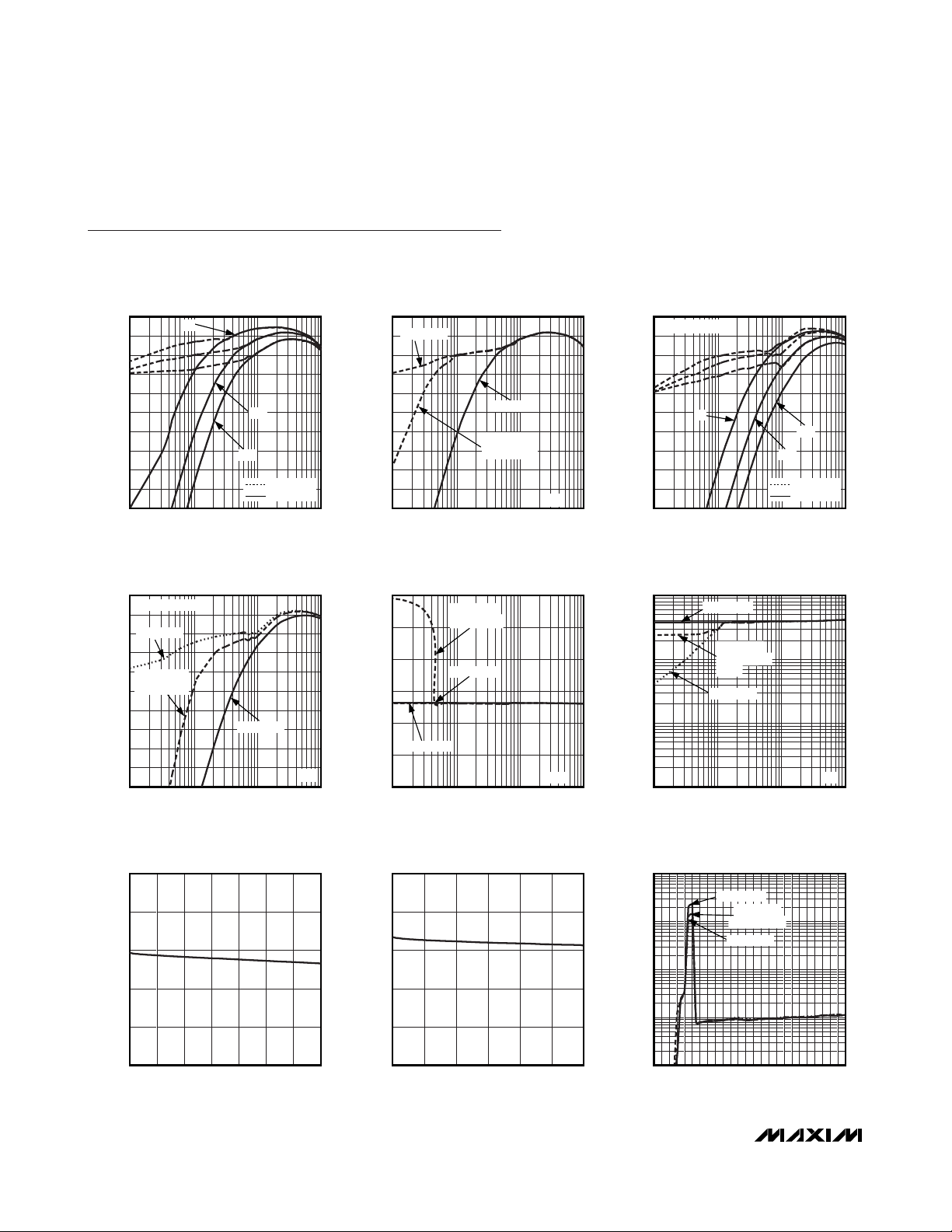
Typical Operating Characteristics
(Circuit of Figure 1, VIN= 12V, VDD= VCC= 5V, TON = REF, TA= +25°C, unless otherwise noted.)
5V OUTPUT EFFICIENCY
vs. LOAD CURRENT
100
95
90
85
80
75
70
EFFICIENCY (%)
65
60
55
50
0.01 10
7V
LOAD CURRENT (A)
3.3V OUTPUT EFFICIENCY
vs. LOAD CURRENT
100
5V SMPS ENABLED
95
SKIP MODE
90
85
80
ULTRASONIC
75
70
EFFICIENCY (%)
65
60
55
50
MODE
0.01 10
LOAD CURRENT (A)
12V
20V
SKIP MODE
PWM MODE
10.1
PWM MODE
10.1
12V
100
SKIP MODE
95
MAX17020 toc01
90
85
80
75
70
EFFICIENCY (%)
65
60
55
50
0.01 10
SMPS OUTPUT VOLTAGE DEVIATION
3
MAX17020 toc04
2
1
0
-1
SKIP MODE
OUTPUT VOLTAGE DEVIATION (%)
-2
-3
0.01 10
5V OUTPUT EFFICIENCY
vs. LOAD CURRENT
PWM MODE
ULTRASONIC
MODE
10.1
LOAD CURRENT (A)
vs. LOAD CURRENT
LOW-NOISE
ULTRASONIC
PWM MODE
10.1
LOAD CURRENT (A)
12V
12V
100
5V SMPS ENABLED
95
MAX17020 toc02
90
85
80
75
70
EFFICIENCY (%)
65
60
55
50
0.01 10
1000
MAX17020 toc05
100
10
SWITCHING FREQUENCY (kHz)
1
0.01 10
3.3V OUTPUT EFFICIENCY
vs. LOAD CURRENT
7V
20V
12V
SKIP MODE
PWM MODE
10.1
LOAD CURRENT (A)
SWITCHING FREQUENCY
vs. LOAD CURRENT
PWM MODE
LOW-NOISE
ULTRASONIC
MODE
SKIP MODE
10.1
LOAD CURRENT (A)
MAX17020 toc03
MAX17020 toc06
12V
5V LDO OUTPUT VOLTAGE
vs. LOAD CURRENT
5.2
5.1
5.0
4.9
OUTPUT VOLTAGE (V)
4.8
4.7
020 140
LOAD CURRENT (mA)
100 12040 60 80
MAX17020 toc07
OUTPUT VOLTAGE (V)
3.3V RTC OUTPUT VOLTAGE
vs. LOAD CURRENT
3.5
3.4
3.3
3.2
3.1
3.0
02 12
LOAD CURRENT (mA)
10468
MAX17020 toc08
NO-LOAD INPUT SUPPLY CURRENT
vs. INPUT VOLTAGE
100
PWM MODE
10
SKIP MODE
1
SUPPLY CURRENT (mA)
0.1
0.01
025
INPUT VOLTAGE (V)
LOW-NOISE
ULTRASONIC
15 20510
MAX17020 toc09
MAX17020
Dual Quick-PWM Step-Down Controller
with Low-Power LDO, RTC Regulator
______________________________________________________________________________________ 11
Typical Operating Characteristics (continued)
(Circuit of Figure 1, VIN= 12V, VDD= VCC= 5V, TON = REF, TA= +25°C, unless otherwise noted.)
STANDBY AND SHUTDOWN INPUT
SUPPLY CURRENT vs. INPUT VOLTAGE
1
STANDBY (ONLDO = VIN)
0.1
SUPPLY CURRENT (mA)
SHUTDOWN
(ONLDO = ON1 = ON2 = GND)
0.01
025
INPUT VOLTAGE (V)
15 20510
70
60
MAX17020 toc10
50
40
30
SAMPLE PERCENTAGE (%)
20
10
0
-20 -4-12 4 12 20
100mV ILIM THRESHOLD
VOLTAGE DISTRIBUTION
50
+85°C
+25°C
40
30
20
SAMPLE PERCENTAGE (%)
10
0
90 9894 102 106 110
ILIM THRESHOLD VOLTAGE (mV)
SAMPLE SIZE = 150
12V
MAX17020 toc13
0V
0V
0V
0V
REFERENCE OFFSET
VOLTAGE DISTRIBUTION
+85°C
+25°C
2V REF OFFSET VOLTAGE (mV)
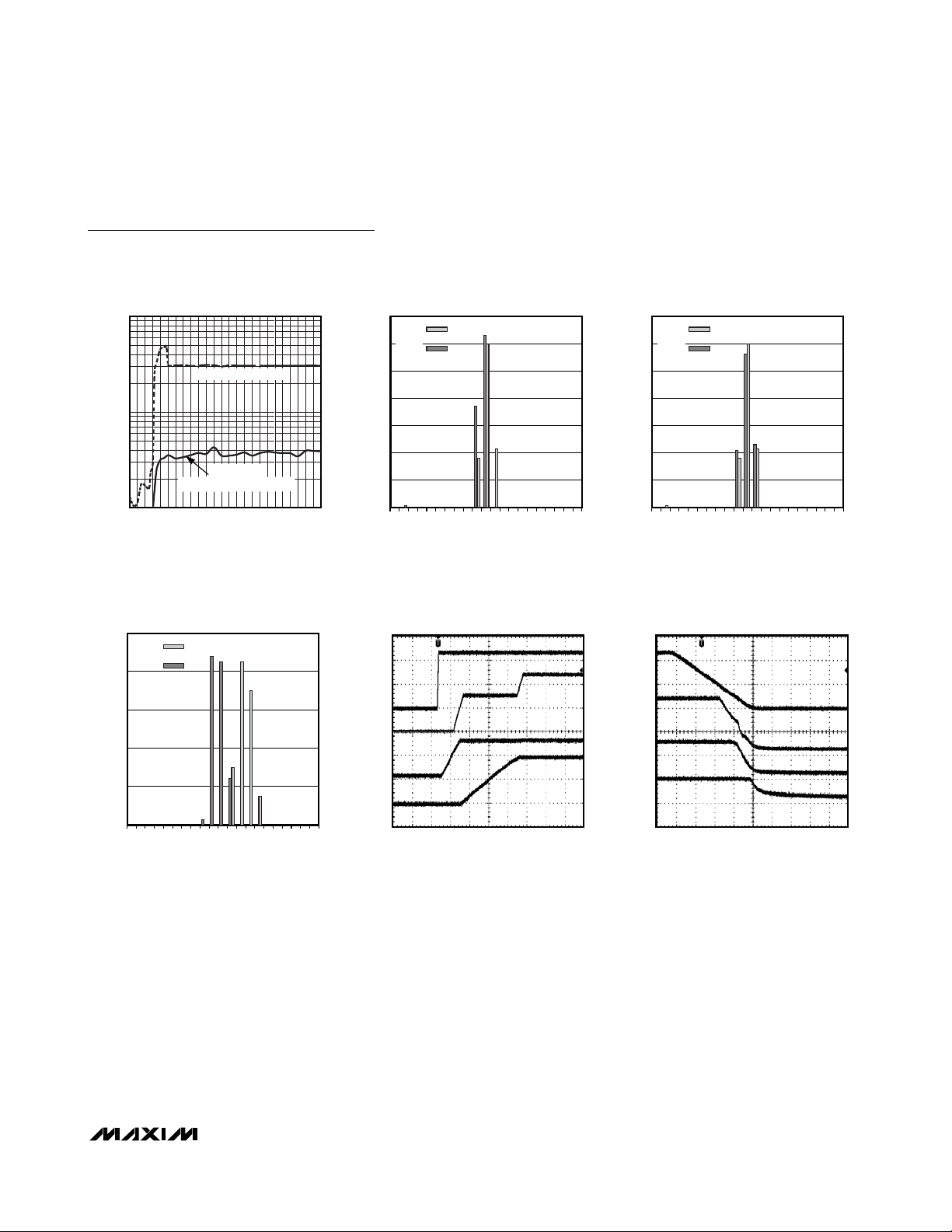
LDO AND RTC POWER-UP
A. INPUT SUPPLY, 5V/div
B. 5V LDO, 2V/div
200μs/div
SAMPLE SIZE = 150
MAX17020 toc14
C. 3.3V RTC, 2V/div
D. 2.0V REF, 1V/div
70
60
MAX17020 toc11
50
40
30
SAMPLE PERCENTAGE (%)
20
10
0
A
12V
12V
B
5V
C
3.3V
D
2.0V
5V
3.3V
2V
REFIN2 OFFSET
VOLTAGE DISTRIBUTION
+85°C
+25°C
-5 -1-3 1 3 5
REFIN2 OFFSET VOLTAGE (mV)
LDO AND RTC POWER REMOVAL
A. INPUT SUPPLY, 5V/div
B. 5V LDO, 2V/div
SAMPLE SIZE = 150
200μs/div
MAX17020 toc15
C. 3.3V RTC, 2V/div
D. 2.0V REF, 1V/div
MAX17020 toc12
A
12V
B
5V
C
3.3V
D
2.0V
 Loading...