

Maxim Integrated MAX17005A, MAX17006A, MAX17015A Datasheet

General Description
The MAX17005A/MAX17006A/MAX17015A are high-frequency multichemistry battery chargers. These circuits
feature a new high-frequency current-mode architecture
that significantly reduces component size and cost*.
The charger uses a high-side MOSFET with n-channel
synchronous rectifier. Widely adjustable charge current,
charge voltage, and input current limit simplify the construction of highly accurate and efficient chargers.
The charge voltage and charge current are set with
analog control inputs. The charge current setting can
also be adjusted with a PWM input. High-accuracy current-sense amplifiers provide fast cycle-by-cycle current-mode control to protect against short circuits to the
battery and respond quickly to system load transients.
In addition, the charger provides a high-accuracy analog output that is proportional to the adapter current. In
the MAX17015A, this current monitor remains active
when the adapter is absent to monitor battery discharge current.
The MAX17005A charges three or four Li+ series cells,
and the MAX17006A charges two or three Li+ series
cells. The MAX17015A adjusts the charge voltage setting and the number of cells through a feedback resistor-divider from the output. All variants of the charger
can provide at least 4A of charge current with a 10mΩ
sense resistor.
The charger utilizes a charge pump to control an n-channel
adapter selection switch. The charge pump remains
active even when the charger is off. When the adapter
is absent, a p-channel MOSFET selects the battery.
The MAX17005A/MAX17006A/MAX17015A are available in a small, 4mm x 4mm x 0.8mm 20-pin, lead-free
TQFN package. An evaluation kit is available to reduce
design time.
Applications
Notebook Computers
Tablet PCs
Portable Equipment with Rechargeable Batteries
Features
o High Switching Frequency (1.2MHz)
o Controlled Inductor Current-Ripple Architecture
Reduced BOM Cost
Small Inductor and Output Capacitors
o ±0.4% Accurate Charge Voltage
o ±2.5% Accurate Input-Current Limiting
o ±3% Accurate Charge Current
o Single-Point Compensation
o Monitor Outputs for
±2.5% Accurate Input Current Limit
±2.5% Battery Discharge Current
(MAX17015A Only)
AC Adapter Detection
o Analog/PWM Adjustable Charge-Current Setting
o Battery Voltage Adjustable for 3 and 4 Cells
(MAX17005A) or 2 and 3 Cells (MAX17006A)
o Adjustable Battery Voltage (4.2V to 4.4V/Cell)
o Cycle-by-Cycle Current Limit
Battery Short-Circuit Protection
Fast Response for Pulse Charging
Fast System-Load-Transient Response
o Programmable Charge Current < 5A
o Automatic System Power Source Selection with
n-Channel MOSFET
o Internal Boost Diode
o +8V to +26V Input-Voltage Range
MAX17005A/MAX17006A/MAX17015A
1.2MHz, Low-Cost,
High-Performance Chargers
________________________________________________________________
Maxim Integrated Products
1
Ordering Information
19-4355; Rev 0; 10/08
For pricing, delivery, and ordering information, please contact Maxim Direct at 1-888-629-4642,
or visit Maxim’s website at www.maxim-ic.com.
+
Denotes a lead-free/RoHS compliant package.
*
Future product—contact factory for availability.
*
*
EP = Exposed pad.
PART TEMP RANGE
PIN-PACKAGE
MAX17005AETP+ -40°C to +85°C 20 TQFN-EP**
-40°C to +85°C 20 TQFN-EP**
MAX17015AETP+ -40°C to +85°C 20 TQFN-EP**
Pin Configuration and Minimal Operating Circuit appear at
end of data sheet.
*
Patent pending.
MAX17006AETP+*
MAX17005A/MAX17006A/MAX17015A
1.2MHz, Low-Cost,
High-Performance Chargers
2 _______________________________________________________________________________________
ABSOLUTE MAXIMUM RATINGS
ELECTRICAL CHARACTERISTICS
(Circuit of Figure 1, V
DCIN
= V
CSSP
= V
CSSN
= 19V, V
BATT
= V
CSIP
= V
CSIN
= 16.8V, V
VCTL
= VAA, V
ISET
= 1V, TA= 0°C to +85°C,
unless otherwise noted. Typical values are at T
A
= +25°C.)
Stresses beyond those listed under “Absolute Maximum Ratings” may cause permanent damage to the device. These are stress ratings only, and functional
operation of the device at these or any other conditions beyond those indicated in the operational sections of the specifications is not implied. Exposure to
absolute maximum rating conditions for extended periods may affect device reliability.
DCIN, CSSP, CSSN, BATT, CSIN, CSIP, ACOK,
LX to AGND .......................................................-0.3V to +30V
BST to LDO.............................................................-0.3V to +30V
CSIP to CSIN, CSSP to CSSN .............................. -0.3V to +0.3V
IINP, FB, ACIN to AGND.............................-0.3V to (V
AA
+ 0.3V)
V
AA
, LDO, ISET, VCTL, CC to AGND .......................-0.3V to +6V
DHI to LX ....................................................-0.3V to (BST + 0.3V)
BST to LX..................................................................-0.3V to +6V
DLO to PGND ............................................-0.3V to (LDO + 0.3V)
PGND to AGND .................................................... -0.3V to +0.3V
Continuous Power Dissipation (T
A
= +70°C)
16-Pin TQFN (derate 16.9mW/°C above +70°C)....1349.1mW
Operating Temperature Range ...........................-40°C to +85°C
Junction Temperature......................................................+150°C
Storage Temperature Range .............................-60°C to +150°C
Lead Temperature (soldering, 10s) .................................+300°C
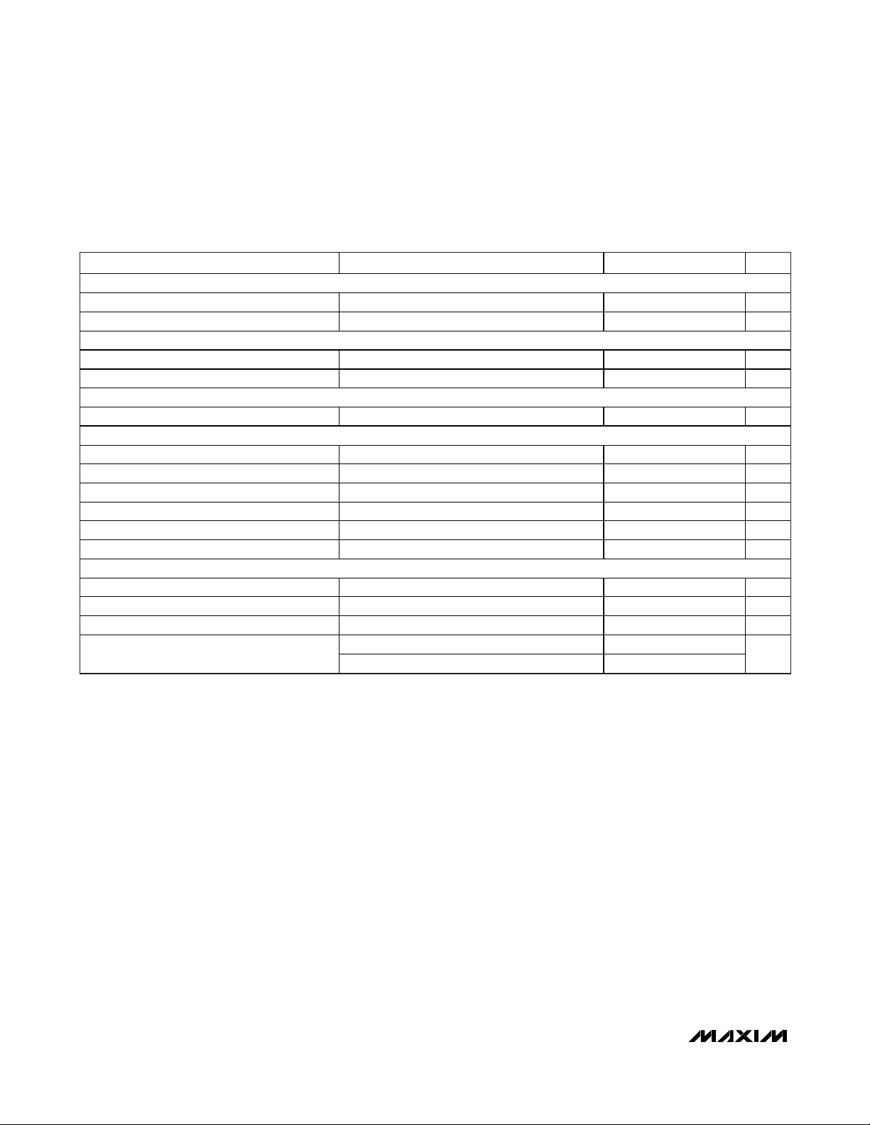
PARAMETER CONDITIONS MIN TYP MAX UNITS
CHARGE-VOLTAGE REGULATION
2 cel ls, V
VCTL
= GND (MAX17006A) 8.3664 8.40 8.4336
3 cells, V
VCTL
= VAA (MAX17005A/MAX17006A) 12.549 12.60 12.651
4 cel ls, V
VCTL
= GND (MAX17005A) 16.733 16.80 16.867
Battery Regulation-Voltage Accuracy
FB accuracy using FB divider (MAX17015A)
(Note 1)
2.0916 2.1 2.1084
V
FB Input Bias Curent -1 +1 μA
2 cells (MAX17006A), 4 cells (MAX17005A) 0
V
AA
/2
-0.2
VCTL Range
3 cells (MAX17005A/MAX17006A)
VAA/2
+0.2
V
AA
V
VCTL Gain V
CELL/VVCTL
5.85 6 6.15 V/V
VCTL Input Bias Current V
VCTL
= GND and VCTL = V
AA
-1 +1 μA
CHARGE-CURRENT REGULATION
ISET Range 0 VAA/2 V
ISET = 1.4V 80
ISET Full-Scale Setting
ISET = 99.9% duty cycle 60
mV
58.2 60 61.8 mV
V
ISET
= VAA/4 or ISET
= 99.9% duty cycle
-3 +3 %
38.2 40 41.8 mV
Ful l-Charge Current Accurac y
(CSIP to CSIN)
V
ISET
= VAA/6 or ISET
= 66.7% duty cycle
-4.5 +4.5 %
1.4 3 4.6 mV
Trickle Charge-Current Accuracy
V
BATT
= 1V to 16.8V
V
ISET
= VAA/80 or ISET
= 5% duty cycle
-52 +52 %
Charge-Current Gain Error Based on V
ISET
= V
VAA
/4 and V
ISET
= V
VAA
/80 -2 +2 %
Charge-Current Offset Error Based on V
ISET
= V
VAA
/4 and V
ISET
= V
VAA
/80 -1.4 +1.4 mV
BATT/CSIP/CSIN Input-Voltage Range 0 24 V
ISET falling 21 26 31
ISET Power-Down Mode Threshold
ISET rising 33 40 47
mV
MAX17005A/MAX17006A/MAX17015A
1.2MHz, Low-Cost,
High-Performance Chargers
_______________________________________________________________________________________ 3
PARAMETER CONDITIONS MIN TYP MAX UNITS
V
ISET
= 3V -0.2 +0.2
ISET Input Bias Current
CSSN = BATT, V
ISET
= 5V -0.2 +0.2
μA
Ri sing 2.4
ISET PWM Threshold
Fal ling 0.8
V
ISET Frequency 0.128 500 kHz
ISET Effecti ve Resolut ion f
PWM
= 3.2MHz 8 Bits
INPUT-CURRENT REGULATION
58.5 60 61.5 mV
Input Current-Limit Thresho ld V
CSSP
- V
CSSN
-2.5 +2.5 %
CSSN Input Bias Current Adapter present -0.1 +0.1 μA
CSSP/CSSN Input-Voltage Range 8.0 26.0 V
IINP Transconductance V
CSSP
- V
CSSN
= 60mV 2.66 2.8 2.94 μA/mV
V
CSSP
- V
CSSN
= 60mV, V
IINP
= 0 to 4.5V -2.5 +2.5
IINP Accuracy
V
CSSP
- V
CSSN
= 35mV -2.5 +2.5
%
SUPPLY AND LINEAR REGULATOR
DCIN Input-Voltage Range 8 26 V
DCIN falling 7.9 8.1
DCIN Undervoltage-Lockout (UVLO) Trip-Point
DCIN rising 8.7 8.9
V
Adapter present (Note 2) 3 6 mA
DCIN + CSSP + CSSN Quiescent Current
Adapter absent (Note 2) 30 50 μA
Adapter absent (Note 2) 10 20
V
BATT
= 16.8V
Charger shutdown (Note 2) 10 20
BATT + CSIP + CSIN + LX Input Current
V
BATT
= 2V to 19V, adapter present (Note 2) 200 500
μA
LDO Output Voltage 8.0V < V
DCIN
< 26V, no load 5.15 5.35 5.55 V
LDO Load Regulation 0 < I
LDO
< 40mA 100 200 mV
LDO UVLO Threshold 3.2 4.1 5.0 V
REFERENCES
VAA Output Voltage I
VAA
= 50μA 4.18 4.20 4.22 V
VAA UVLO Threshold VAA falling 3.1 3.9 V
ACIN
ACIN Thresho ld 2.058 2.1 2.142 V
ACIN Threshold Hysteresi s 10 20 30 mV
ACIN Input Bias Current -1 +1 μA
ACOK
ACOK Sink Current V
ACOK
= 0.4V, V
ACIN
= 1.5V 6 mA
ACOK Leakage Current V
ACOK
= 5.5V, V
ACIN
= 2.5V 1 μA
ELECTRICAL CHARACTERISTICS (continued)
(Circuit of Figure 1, V
DCIN
= V
CSSP
= V
CSSN
= 19V, V
BATT
= V
CSIP
= V
CSIN
= 16.8V, V
VCTL
= VAA, V
ISET
= 1V, TA= 0°C to +85°C,
unless otherwise noted. Typical values are at T
A
= +25°C.)
MAX17005A/MAX17006A/MAX17015A
1.2MHz, Low-Cost,
High-Performance Chargers
4 _______________________________________________________________________________________
PARAMETER CONDITIONS MIN TYP MAX UNITS
SWITCHING REGULATOR
DHI Off-Time K Factor V
DCIN
= 19V, V
BATT
= 10V 0.029 0.030 0.041 μs/V
Sense Voltage for Minimum Discontinuous
Mode Ripple Current
V
CSIP
- V
CSIN
10 mV
Zero-Crossing Comparator Threshold V
CSIP
- V
CSIN
10 mV
Cycle-by-Cycle Current-Limit Sense Voltage V
CSIP
- V
CSIN
105 110 115 mV
DHI Resistance High I
DLO
= 10mA 1.5 3
DHI Resistance Low I
DLO
= -10mA 0.8 1.75
DLO Resistance High I
DLO
= 10mA 3 6
DLO Resistance Low I
DLO
= -10mA 3 7
ADAPTER DETECTION
Adapter Absence-Detect Threshold V
DCIN
- V
BATT
, V
DCIN
falling +70 +120 +170 mV
Adapter Detect Threshold V
DCIN
- V
BATT, VDCIN
rising +360 +420 +580 mV
Adapter Switch C harge-Pump Frequency Charger Shutdown 180 200 220 Hz
DLO 0.04 0.1 0.20
Adapter Switch Charge-Pump Refresh Pulse
DHI 0.07 0.15 0.30
μs
ELECTRICAL CHARACTERISTICS (continued)
(Circuit of Figure 1, V
DCIN
= V
CSSP
= V
CSSN
= 19V, V
BATT
= V
CSIP
= V
CSIN
= 16.8V, V
VCTL
= VAA, V
ISET
= 1V, TA= 0°C to +85°C,
unless otherwise noted. Typical values are at T
A
= +25°C.)
ELECTRICAL CHARACTERISTICS
(Circuit of Figure 1, V
DCIN
= V
CSSP
= V
CSSN
= 19V, V
BATT
= V
CSIP
= V
CSIN
= 16.8V, V
VCTL
= VAA, V
ISET
= 1V, TA= -40°C to +85°C,
unless otherwise noted.)
PARAMETER CONDITIONS MIN TYP MAX UNITS
CHARGE-VOLTAGE REGULATION
2 cel ls, V
VCTL
= GND (MAX17006A) 8.366 8.433
3 cel ls, V
VCTL
= VAA (MAX17005A/MAX17006A) 12.549 12.651
4 cel ls, V
VCTL
= GND (MAX17005A) 16.73 16.86
Battery Regulation-Voltage Accuracy
FB accuracy using FB divider (MAX17015A)
(Note 1)
2.091 2.108
V
2 cells (MAX17006A),
4 cells (MAX17005A)
0.
V
AA
/2
- 0.2
VCTL Range
3 cells (MAX17005A/MAX17006A)
V
AA
/2
+ 0.2
V
AA
V
VCTL Gain V
CELL/VVCTL
5.85 6.15 V/V
MAX17005A/MAX17006A/MAX17015A
1.2MHz, Low-Cost,
High-Performance Chargers
_______________________________________________________________________________________ 5
ELECTRICAL CHARACTERISTICS (continued)
(Circuit of Figure 1, V
DCIN
= V
CSSP
= V
CSSN
= 19V, V
BATT
= V
CSIP
= V
CSIN
= 16.8V, V
VCTL
= VAA, V
ISET
= 1V, TA= -40°C to +85°C,
unless otherwise noted.)
PARAMETER CONDITIONS MIN TYP MAX UNITS
CHARGE-CURRENT REGULATION
ISET Range 0 VAA/2 V
57.5 62.5 mV
V
ISET
= VAA/4 or
ISET = 99.9% duty cycl e
-4.2 +4.2 %
38 42 mV
Ful l Charge-Current Accurac y
(CSIP to CSIN)
V
ISET
= VAA/6 or
ISET = 66.7% duty cycl e
-5 +5 %
1.4 4.6 mV
Trickle Charge-Current Accuracy
V
BATT
= 1V to 16.8V
V
ISET
= VAA/80 or
ISET = 5% duty cycle
-52 +52 %
Charge-Current Gain Error Based on V
ISET
= V
VAA
/4 and V
ISET
= V
VAA
/80 -2 +2 %
Charge-Current Offset Error Ba sed on V
ISET
= V
VAA
/4 and V
ISET
= V
VAA
/80 -1.4 +1.4 mV
BATT/CSIP/CSIN Input-Voltage Range 0 24 V
ISET falling 21 31
ISET Power-Down Mode Threshold
ISET ris ing 33 47
mV
Ri sing 2.4
ISET PWM Threshold
Fal ling 0.8
V
ISET Frequency 0.128 500 kHz
INPUT-CURRENT REGULATION
58.2 61.8 mV
Input Current-Limit Thresho ld V
CSSP
- V
CSSN
-3 +3 %
CSSN Input Bias Current Adapter present -2 +2 μA
CSSP/CSSN Input-Voltage Range 8.0 26.0 V
IINP Transconductance V
CSSP
- V
CSSN
= 60mV 2.66 2.94 μA/mV
V
CSSP
- V
CSSN
= 60mV, V
IINP
= 0 to 4.5V -2.5 +2.5
IINP Accuracy
V
CSSP
- V
CSSN
= 35mV -2.5 +2.5
%
SUPPLY AND LINEAR REGULATOR
DCIN Input-Voltage Range 8 26 V
DCIN falling 7.9
DCIN UVLO Trip-Point
DCIN rising 8.9
V
Adapter present (Note 2) 6 mA
DCIN + CSSP + CSSN Quiescent Current
Adapter absent (Note 2) 50 μA
Adapter absent (Note 2) 20
V
BATT
= 16.8V
Charger shutdown (Note 2) 20
BATT + CSIP + CSIN + LX Input Current
V
BATT
= 2V to 19V, adapter present (Note 2) 500
μA
LDO Output Voltage 8.0V < V
DCIN
< 26V, no load 5.15 5.55 V
LDO Load Regulation 0 < I
LDO
< 40mA 200 mV
LDO UVLO Threshold 3.2 5.0 V
MAX17005A/MAX17006A/MAX17015A
1.2MHz, Low-Cost,
High-Performance Chargers
6 _______________________________________________________________________________________
ELECTRICAL CHARACTERISTICS (continued)
(Circuit of Figure 1, V
DCIN
= V
CSSP
= V
CSSN
= 19V, V
BATT
= V
CSIP
= V
CSIN
= 16.8V, V
VCTL
= VAA, V
ISET
= 1V, TA= -40°C to +85°C,
unless otherwise noted.)
PARAMETER CONDITIONS MIN TYP MAX UNITS
REFERENCES
VAA Output Voltage I
VAA
= 50μA 4.18 4.22 V
VAA UVLO Thresho ld VAA falling 3.9 V
ACIN
ACIN Thresho ld 2.058 2.142 V
ACIN Thresho ld Hysteresis 10 30 mV
ACOK
ACOK Sink Current V
ACOK
= 0.4V, V
ACIN
= 1.5V 6 mA
SWITCHING REGULATOR
DHI Off-Time K Factor V
DCIN
= 19V, V
BATT
= 10V 0.029 0.041 μs/V
Cycle-by-Cycle Current-Limit Sense Voltage V
CSIP
- V
CSIN
105 115 mV
DHI Resistance High I
DLO
= 10mA 3
DHI Resistance Low I
DLO
= -10mA 1.75
DLO Resistance High I
DLO
= 10mA 6
DLO Resistance Low I
DLO
= -10mA 7
ADAPTER DETECTION
Adapter Absence-Detect Threshold V
DCIN
- V
BATT
, V
DCIN
falling +70 +170 mV
Adapter Detect Threshold V
DCIN
- V
BATT, VDCIN
rising +320 +620 mV
Adapter Switch C harge-Pump Frequency 180 220 Hz
DLO 0.04 0.2
Adapter Switch Charge-Pump Refresh Pulse
DHI 0.07 0.3
μs
Note 1: Accuracy does not include errors due to external resistance tolerances.
Note 2: Adapter present conditions are tested at V
DCIN
= 19V and V
BATT
= 16.8V. Adapter absent conditions are tested at
V
DCIN
= 16V, V
BATT
= 16.8V.
MAX17005A/MAX17006A/MAX17015A
1.2MHz, Low-Cost,
High-Performance Chargers
_______________________________________________________________________________________ 7
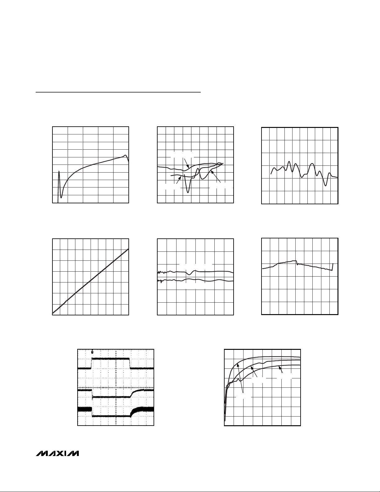
Typical Operating Characteristics
(Circuit of Figure 1, adapter = 19V, battery = 10V, ISET = 1.05V, V
CTL
= GND, TA= +25°C, unless otherwise noted.)
IINP DC ERROR
vs. SYSTEM CURRENT
MAX17005A toc01
SYSTEM CURRENT (A)
IINP ERROR (%)
4312
-8
-6
-4
-2
0
2
4
6
8
10
-10
05
IINP ERROR
vs. SYSTEM CURRENT
MAX17005A toc02
SYSTEM CURRENT (A)
IINP ERROR (%)
4.03.52.5 3.01.0 1.5 2.00.5
-8
-6
-4
-2
0
2
4
6
8
10
-10
04.5
V
BATT
= 16.8V
V
BATT
= 8.4V
V
BATT
= 12.6V
ISET PWM DUTY-CYCLE CHANGE
MAX17005A toc03
DUTY CYCLE
CHARGE-CURRENT ERROR (%)
0.8 0.90.1 0.2 0.3 0.4 0.5 0.6 0.7
0.5
1.0
1.5
2.0
2.5
3.0
0
01.0
ISET PWM DUTY-CYCLE CHANGE
MAX17005A toc04
DUTY CYCLE
CHARGE CURRENT (A)
80 9010 20 30 40 50 60 70
0.5
1.0
1.5
2.0
2.5
3.0
3.5
0
0100
ISET PWM FREQUENCY SWEEP
MAX17005A toc05
FREQUENCY (kHz)
CHARGE-CURRENT ERROR (%)
600 700100 200 300 400 500
0.5
1.0
1.5
2.0
2.5
3.0
0
0 800
DUTY CYCLE = 75%
DUTY CYCLE = 25%
BATTERY VOLTAGE-SETTING ERROR
MAX17005A toc06
VCTL (V)
BATTERY VOLTAGE ERROR (%)
3.0 3.5 4.00.5 1.0 1.5 2.0 2.5
-0.5
-0.4
-0.3
-0.2
-0.1
0
-0.6
04.5
SYSTEM LOAD TRANSIENT
MAX17005A toc07
200μs/div
SYSTEM
CURRENT
5A/div
CHARGING
CURRENT
5A/div
INDUCTOR
CURRENT
5A/div
EFFICIENCY
vs. CHARGE CURRENT
MAX17005A toc08
CHARGE CURRENT (A)
EFFICIENCY (%)
2.5 3.0 3.50.5 1.0 1.5 2.0
70
65
75
80
85
95
90
100
60
04.0
2 CELLS
3 CELLS
4 CELLS
 Loading...