

Page 1
General Description
The MAX1402 evaluation system (EV system) is a complete, multichannel data-acquisition system consisting of
a MAX1402 evaluation kit (EV kit), Maxim 68HC16 microcontroller (µC) module, and USBT0232. The MAX1402 is
a low-power, multichannel, serial-output analog to digital
converter (ADC). Windows
®
98/2000/XP-compatible software provides a handy user interface to exercise the
MAX1402’s features. Source code in C++ and 68HC11
assembly language is provided for the low-level portion of
the software.
Order the EV system for comprehensive evaluation of
the MAX1402 using a personal computer. Order only
the EV kit if the 68HC16 µC module has already been
purchased with a previous Maxim EV system, or for
custom use in other µC-based systems.
The MAX1402 EV kit and EV system can also be used
to evaluate the MAX1400. Simply order a free sample of
the MAX1400CAI along with the MAX1402 EV kit.
MAX1402 Stand-Alone EV Kit
The MAX1402 EV kit provides a proven printed-circuit
board (PCB) layout to facilitate evaluation of the
MAX1402 with user-supplied software and hardware. It
must be interfaced to appropriate timing signals for
proper operation. Refer to the MAX1402 IC data sheet
for timing requirements. See Table 2, Jumper Functions.
MAX1402 EV System
The MAX1402 EV system operates from a user-supplied
+8V to +12VDC power supply.
Features
♦ Easy to Configure
♦ Collects Up to 8192 Samples at Full Speed
♦ Complete Evaluation System
♦ Proven PCB Layout
♦ Fully Assembled and Tested
♦ EV Kit Software Supports Windows 98/2000/XP
with RS-232/COM Port
♦ EV Kit Software Supports Windows 2000/XP with
USB Port
Evaluate: MAX1400/MAX1402
MAX1402 Evaluation Kit/Evaluation System
________________________________________________________________ Maxim Integrated Products 1
19-1440; Rev 2; 5/07
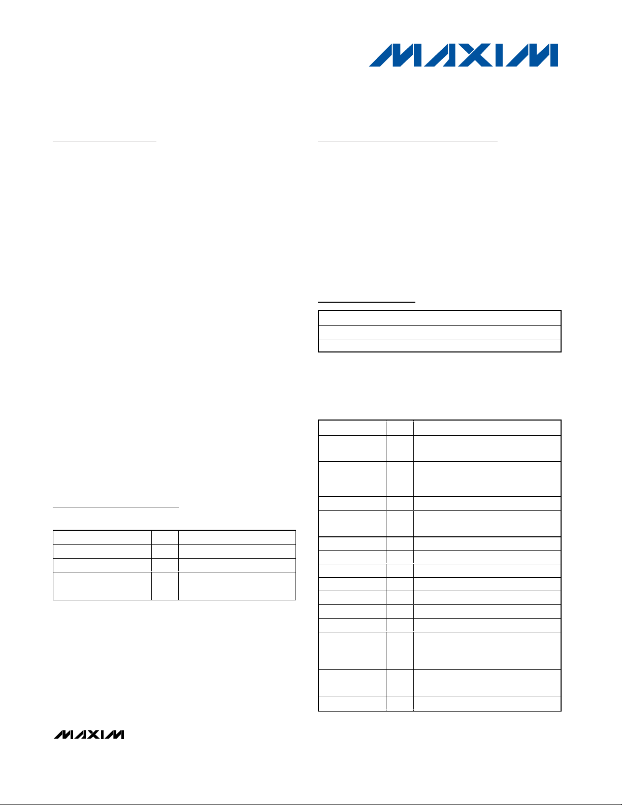
Component Lists
MAX1402 EV System
For pricing, delivery, and ordering information, please contact Maxim Direct at 1-888-629-4642,
or visit Maxim’s website at www.maxim-ic.com.
Ordering Information
MAX1402 EV Kit
Windows is a registered trademark of Microsoft Corp.
Note: The MAX1402 software can only be used with the complete evaluation system (MAX1402EVC16), which includes the
68HC16MODULE-DIP, USBTO232, and the MAX1402EVKIT.
+Denotes lead-free and RoHS-compliant.
PART QTY DESCRIPTION
MAX1402EVKIT 1 MAX1402 EV kit
68HC16MODULE-DIP 1 68HC16 µC module
USBTO232+ 1
USB-to-COM port adapter
board
PART TYPE RANGE INTERFACE TYPE
MAX1402EVKIT 0°C to +70°C User supplied
MAX1402EVC16 0°C to +70°C Windows software
PART QTY DESCRIPTION
C3–C8 6
C9, C10, C11 3
C12, C13 2 Not installed, capacitors
C15 1
J1 1 2 x 20 right-angle socket
J2 1 Female SMA connector
JU1–JU8 0 Not installed
R1–R6 6 100Ω ±5% resistors (1206)
R7, R8 2 10Ω ±5% resistors (1206)
R9, R10 2 Not installed, resistors
U1 1 MAX1402CAI (28-pin SSOP)
U2 1
Y1 1
— 1 PCB: MAX1402 Evaluation Kit+
100pF ceramic capacitors (1206)
TDK C3216C0G2J101K
0.1µF ceramic capacitors (1206)
Murata GRM319R71H104K
TDK C3216X7R1H104K
2.2µF, 25V X7R ceramic capacitor
TDK C3216X7R1E225K
MAX6025AEUR (SOT23)
2.500V voltage reference
(200ppm/°C max)
2.4576MHz ceramic resonator
Murata CSTCC2M45G53-R0
Page 2

Evaluate: MAX1400/MAX1402
MAX1402 Evaluation Kit/Evaluation System
2 _______________________________________________________________________________________
Quick Start
Recommended Equipment (USB Port/PC
Connection Option)
Before beginning, the following equipment is needed:
• MAX1402 EV system:
MAX1402 EV kit
68HC16MODULE-DIP
USBTO232 (USB cable included)
• A DC power supply that generates +8VDC to
+12VDC at 30–50mA
• A user-supplied Windows 2000/XP computer with an
available USB port to connect to the USBTO232
board
Note: In the following sections, software-related items
are identified by bolding. Text in bold refers to items
directly from the EV kit software. Text in bold and
underlined refers to items from the Windows 2000/XP
operating system.
Connections and Setup
The MAX1402 EV kit is fully assembled and tested.
Follow the steps below to verify board operation.
Caution: Do not turn on the power supply until all
connections are completed.
1) Visit the Maxim website (www.maxim-ic.com) to
download the latest version of the USBTO232 User
Guide. Follow the steps in the USBTO232 User
Guide Quick Start section and return to step 2 of
this Quick Start section when finished.
2) Make sure your 68HC16MODULE-DIP module has
the Rev. 2.0 ROM. The software will not function
with the Rev. 1.0 ROM.
3) Carefully connect the boards by aligning the 40-pin
header of the MAX1402 EV kit with the 40-pin connector of the 68HC16MODULE-DIP module. Gently
press them together. The two boards should be
flush against one another.
4) Connect the DC power source to the µC module at
terminal block J2, located next to the ON/OFF
Example Source Code Files
68HC16 Source Code Files
Header file for MAX1402.CPP, provided for
reference.
MAX1402.H
Source code module for driving the
MAX1402, provided for reference. Includes
definitions of the register names and lowlevel access routines. Compiled with
Borland C++ 4.52. Maxim holds the copyright, but allows customers to adapt the
program for their own use without charge.
MAX1402.CPP
Source code defining the program interface with the Maxim 68HC16 Module ROM
(Rev. 2.0).
EVKIT.ASM
Main source code for the KIT1402.C16 program, provided for reference. Maxim holds
the copyright, but allows customers to
adapt the program for their own use without
charge.
KIT1402.ASM
MAX1402 EV Kit Files
Windows Application Program Files
Program settings fileMAX1402.INI
Software loaded into 68HC16 microcontroller.
KIT1402.C16
Help fileMAX1402.HLP
Application program that runs under
Windows 98/2000/XP.
MAX1402.EXE
DESCRIPTIONFILE
DESCRIPTIONFILE
DESCRIPTIONFILE
Note: Indicate that you are using the MAX1402 when contacting these component suppliers.
Component Suppliers
SUPPLIER PHONE FAX WEBSITE
Murata Mfg. Co., Ltd. 770-436-1300 770-436-3030 www.murata.com
TDK Corp. 847-803-6100 847-390-4405 www.component.tdk.com
Page 3

switch, along the top-edge of the µC module.
Observe the polarity marked on the board.
5) Connect the USBTO232 board to the 68HC16MODULEDIP module if you have not done so already.
6) The MAX1402 EV kit software should have already
been downloaded and installed in the USBTO232
Quick Start.
7) Start the MAX1402 program by opening its icon in
the Start | Programs menu.
8) Turn on power supply and slide SW1 to the ON
position on the 68HC16MODULE-DIP module.
Press the OK button to automatically connect and
download the KIT1402.C16 file to the module.
9) When the software successfully establishes communication with the EV kit board, you will see a configuration tool and some other windows. Verify that
the CLKIN and reference voltage settings are correct. Close or minimize this dialog box.
10) Apply input signals to the inputs labeled
AIN1–AIN5, at the bottom-edge of the MAX1402 EV
kit board. AIN6 is analog common. Observe the
readout on the screen.
Recommended Equipment (RS-232-to-COM
Port/PC Connection Option)
Before beginning, the following equipment is needed:
• MAX1402 EV system:
MAX1402 EV kit
68HC16MODULE-DIP
• A DC power supply that generates +8VDC to
+12VDC at 30–50mA
• A user-supplied Windows 98/2000/XP computer with
an available serial communications port, preferably a
9-pin plug
• A serial cable to connect the computer’s serial port to
the 68HC16MODULE-DIP
Note: In the following sections, software-related items
are identified by bolding. Text in bold refers to items
directly from the EV kit software. Text in bold and
underlined refers to items from the Windows
98/2000/XP operating system.
Connections and Setup
1) Visit the Maxim website (www.maxim-ic.com/evkitsoftware) to download the latest version of the EV
kit software. Save the EV kit software to a temporary
folder and uncompress the file (if it is a .zip file).
2) Install the MAX1402 EV kit software on your computer by running the INSTALL.EXE program. The
program files are copied and icons are created for
them in the Windows Start | Programs menu.
3) Make sure your 68HC16MODULE-DIP module has
the Rev. 2.0 ROM. The software will not function with
the Rev. 1.0 ROM.
4) Carefully connect the boards by aligning the 40-pin
header of the MAX1402 EV kit with the 40-pin connector of the 68HC16MODULE-DIP module. Gently
press them together. The two boards should be
flush against one another.
5) Connect the DC power source to the µC module at
terminal block J2, located next to the ON/OFF
switch, along the top-edge of the µC module.
Observe the polarity marked on the board.
6) Connect a cable from the computer’s serial port to
the µC module. If using a 9-pin serial port, use a
straight-through, 9-pin female-to-male cable. If the
only available serial port uses a 25-pin connector, a
standard 25-pin-to-9-pin adapter will be required.
The EV kit software checks the modem status lines
(CTS, DSR, and DCD) to confirm that the correct
port has been selected.
7) Start the MAX1402 program by opening its icon in
the Start | Programs
menu.
8) Turn the power on and slide SW1 to the ON position. Select the correct serial port and press the OK
button. The program will automatically download
KIT1402.C16 to the module.
9) When the software successfully establishes communication with the EV kit board, you will see a configuration tool and some other windows. Verify that
the CLKIN and reference voltage settings are correct. Close or minimize this dialog box.
Evaluate: MAX1400/MAX1402
MAX1402 Evaluation Kit/Evaluation System
_______________________________________________________________________________________ 3
FILE DESCRIPTION
INSTALL.EXE Installs the EV kit files on your computer.
UNINST.INI Database for uninstall program.
Removes the EV kit files from your
UNMAXIM.EXE
computer. This file is automatically copied
to C:\WINDOWS during installation.
FILE DESCRIPTION
INSTALL.EXE Installs the EV kit files on your computer.
UNINST.INI Database for uninstall program.
Removes the EV kit files from your
UNMAXIM.EXE
computer. This file is automatically copied
to C:\WINDOWS during installation.
Page 4

Evaluate: MAX1400/MAX1402
10) Apply input signals to the inputs labeled
AIN1–AIN5, at the bottom-edge of the MAX1402 EV
kit board. AIN6 is analog common. Observe the
readout on the screen.
Upgrading the 68HC16 Module
The MAX1402 EV kit requires Rev. 2.0 of the Maxim
68HC16 Module ROM. Check the label on device U3
on the module; if its label says Rev. 1.0, contact the
factory for a replacement.
To install the new ROM, use the following procedure.
Use antistatic handling precautions. To reduce the risk
of ESD damage, gather all required materials and perform the installation at one sitting:
1) Slide the ON/OFF switch to the OFF position.
2) Using a flat-blade screwdriver, gently pry U3, the
REV 1.0 ROM, out of its socket.
3) Remove the REV 2.0 ROM from its antistatic packaging.
4) Align the REV 2.0 ROM in the U3 socket pins.
Observe correct polarity (the notch at the top of the
ROM). Verify that the pins are lined up with the
socket, and gently press the ROM into place.
Proceed to the regular Quick Start instructions.
Detailed Description
_________________________of Software
The MAX1402 digitizes up to seven inputs. The various
program functions are grouped into windows, which are
accessible from the Show menu on the main menu bar.
Main Display
The main display shows the calculated input voltage
and raw A/D output code for each active channel.
Although there are nine input channels, only certain
configurations are allowed.
Select any single channel or one of the scanning
sequences from the Inputs menu. AIN 1-6 designates
an analog input between the AIN1 pin and the AIN6 pin.
CALOFF designates the signal between the CALOFF+
and CALOFF- pins. CALGAIN designates the signal
between the CALGAIN+ and CALGAIN- pins.
The EV kit software assumes that CALOFF+ and
CALOFF- are grounded so that CALOFF measures zero
volts. Similarly, the software assumes that CALGAIN+ is
connected to REFIN+ and CALGAIN- is connected to
REFIN- so that CALGAIN measures the reference voltage. These two points calibrate the code-to-voltage
translation function performed in the software.
The MAX1400/MAX1402 automatically triggers its measurements, unless the FSYNC control bit is set. The
evaluation kit software communicates with the
MAX1400/MAX1402 at intervals determined by the
Update Every combo box. To halt this automatic update,
uncheck the Update Every checkbox or change the
Update Every to a value between 100ms and 60000ms.
Normally, the microcontroller collects new data as soon
as it becomes available, by using the INT pin to trigger
an interrupt service routine. If the INT pin is not used as
an interrupt, then the MAX1400 must not be operated in
free-running mode. Check or uncheck the Use INT
Interrupt checkbox to configure the evaluation kit software.
Configuration Tool
The Configuration Tool controls parameters that apply
to the entire EV kit. Like the other windows, the
Configuration Tool can be activated from the Show
menu of the main menu bar. The CLK control should
match the external ceramic resonator or crystal that
sets the master clock frequency. The VREF Reference
Voltage control tells the software what the reference
voltage is. This is used to convert the raw A/D output
codes into the corresponding input voltage to speed
user evaluation. The Data Rate control determines how
often the MAX1402 performs a measurement. Some
data rates provide 16-bit, noise-free resolution when
used with the SINC3 filter (discussed below). The Filter
Sync control can be used to inhibit the MAX1402 from
performing its self-timed measurements. The Buffer
Inputs checkbox enables the internal input buffers. The
Burnout Test Currents checkbox enables two small
(0.1µA) current sources to provide an input stimulus.
When used with a transducer, these current sources
can be used to verify that the transducer has not failed
open or short circuit.
At the bottom of the window, there are input voltage
range selection buttons. These buttons configure all
input channels for the same input voltage range.
Although the MAX1400/MAX1402 can be operated with
three different input ranges at the same time, the evaluation kit software only supports a single range for all
channels.
The digital filter on the MAX1402 can be configured for
SINC
3
or SINC1operation, which affects the filter cutoff
frequency. (SINC' means SIN(X) ÷ X, and SINC3means
(SIN(X) ÷ X)3.) The SINC3filter is required for 16-bit accuracy. The SINC1filter provides faster settling time with less
accuracy. Alternatively, the raw modulator output can be
driven out the DOUT pin; however, the EV kit software
cannot read data from the MAX1402 in this mode.
MAX1402 Evaluation Kit/Evaluation System
4 _______________________________________________________________________________________
Page 5

Calibration Tool
The MAX1402 EV kit software can average the measurements from the calibration channels and use the
measured values to correct the voltage displays. The
calibration algorithm assumes that the CALOFF inputs
are externally connected together, and that the
CALGAIN inputs are externally connected to the reference voltage (VREF). View the calibration tool by
selecting it from the Show menu.
The software automatically disables calibration if either
of the calibration channels reports a code of 0 or
262143. This is to prevent erroneous calibration when
using a transfer function that does not include both 0V
and VREF.
When Use CALOFF and CALGAIN for Calibration is
checked, the software averages the raw A/D codes for
the CALOFF and CALGAIN channels. The average is
calculated as a weighted sum of the new data and the
old average value. The Slower/Faster slide bar controls
the weight of the new data vs. the weight of the old
average.
The EV kit software assumes that all three transfer function registers are set to the same value.
This calibration affects only the displayed voltage, not
the raw code numbers. The average CALOFF and
CALGAIN code values are used as the endpoints of a
linear interpolation, with CALOFF measuring zero volts
and CALGAIN measuring VREF.
The linear interpolation formula is as follows:
Sampling Tool
To sample data at full speed, select Sample from the
main display menu, make your selections, and click on
the Begin Sampling button. Sampling rate is controlled
by the Configuration tool. Sample size is restricted to a
power of two. Sample Size controls the number of samples collected on each selected channel. After the
samples have been collected, the data is automatically
uploaded to the host and is graphed. Once displayed,
the data may be saved to a file.
While the Sampling tool is open, the other windows are
locked out. Close the Sampling tool by clicking the
Close icon in the upper corner.
Register Display Tool
This tool displays all of the internal registers of the
MAX1400/MAX1402. Modify any bit value by checking
or unchecking its box. (The START bit and the zero bits
in the special function register (SFR) cannot be modified). The Read All Registers button causes the software to read all of the MAX1400/MAX1402’s registers.
(Not functional when the MDOUT or FULLPD bit is set.)
Refer to Table 4, Guide to Register Bit Functions.
Communications Register (COMMS)
Setting the FSYNC control bit inhibits the MAX1400/
MAX1402 from performing its self-timed measurements.
If FSYNC = 1 when it is time to perform a measurement,
the MAX1400/MAX1402 simply skips that measurement. Thus, power line frequency rejection is not affected by the FSYNC bit.
Setting the STDBY bit places the part in low-power
standby mode. The serial interface and the CLK oscillator continue to operate. The part can be restored to
normal operation by clearing the STDBY bit.
Special Function Register (SFR)
Setting the MDOUT bit causes the raw modulator output
to be driven out the DOUT pin; however, the EV kit software cannot read data from the MAX1402 in this mode.
Setting the FULLPD bit in the SFR register places the
part in full power-down mode. The master oscillator
does not run. To restore normal operation, click on the
Reset menu item in the main display. This causes the
68HC16 software to pulse the MAX1402 RESET pin.
Transfer Function Registers (TF1, TF2, TF3)
The three Transfer Function registers (TF1, TF2, TF3)
control how input voltage is mapped to code values. The
transfer function registers control a programmable-gain
amplifier (PGA) and an offset correction DAC.
If U/B = 1, the transfer function maps unipolar voltages
between 0V and VREF. If U/B = 0, then the transfer
function maps bipolar voltages between -VREF and
+VREF. Next, the PGA increases the code-per-volt processing gain, reducing the full-scale voltage range by a
factor of 1, 2, 4, 8, 16, 32, 64, or 128. Finally, the offset
correction DAC offsets the voltage range by up to ±7/6
of the full-scale voltage range.
Input pins AIN1 and AIN2 are controlled by TF1. Input
pins AIN3 and AIN4 are controlled by TF2. Input pin
AIN5 is controlled by TF3. Input pin AIN6 is the analog
common.
When SCAN = 1, the CALOFF and CALGAIN channels
are controlled by TF3. When SCAN = 0, the CALOFF
and CALGAIN channels are controlled by one of the
transfer function registers, as selected by the A1 and
A0 bits.
Evaluate: MAX1400/MAX1402
MAX1402 Evaluation Kit/Evaluation System
_______________________________________________________________________________________ 5
Voltage
=
()
CALGAINcode CALOFFcode PGAgain
⋅
VREF Code CALOFFcode
()
−
⋅
−
Page 6

Evaluate: MAX1400/MAX1402
MAX1402 Evaluation Kit/Evaluation System
6 _______________________________________________________________________________________
For simplicity, the EV kit software assumes that all three
transfer functions are configured alike.
Detailed Description
________________________of Hardware
U1, the MAX1402, is a multichannel, high-resolution
A/D converter (refer to the MAX1402 data sheet). U2,
the MAX6025, is a 2.5V reference (refer to the
MAX6025 data sheet). Y1 contains a ceramic resonator
and its load capacitors. R1–R6 together with C3–C8
form anti-aliasing input filters. R8 and C11 filter the digital power supply. The analog supply comes through filter R7/C10.
Input Filtering
The EV kit has an RC filter on each input with a time
constant of approximately 0.01µs = 10ns (R = 100Ω,
C = 100pF). When scanning between channels, the RC
filter’s settling time may increase the acquisition time
required for full accuracy.
Evaluating the MAX1400
The MAX1400 can be evaluated by shorting across
jumpers JU6 and JU7. The MAX1400 is exactly like the
MAX1402, except that the function of pins 5, 6, 7, and 8
is changed. Instead of the OUT1/OUT2 outputs and
DS0/DS1 inputs, these pins are used to provide access
to the analog signal between the multiplexer and the
A/D converter. Tables 2 and 3 list the jumper functions
and default settings. Refer to the MAX1400 data sheet
for detailed information.
Measuring Supply Current
Supply current can be estimated by measuring the voltage across a series resistor. On the EV kit board, the
MAX1402 draws all of its analog and digital power
through R8, which is 10Ω. In addition, all analog supply
current flows through R7, which is also 10Ω.
Troubleshooting
Problem: unacceptable amounts of noise in the signal.
Collect a sample of 1024 measurements at a 60Hz data
rate. Observe whether the problem is caused by 60Hz
noise.
Any AC-powered equipment connected to the analog
signal ground can inject noise. Try replacing AC-powered DVMs with battery-powered DVMs.
Page 7

Evaluate: MAX1400/MAX1402
MAX1402 Evaluation Kit/Evaluation System
_______________________________________________________________________________________ 7
Table 3. Default Jumper Settings
*Default trace on top layer of PCB.
JUMPER STATE FUNCTION
JU1 Closed* Use CalGain inputs for gain calibration (CALGAIN+ = REFIN+)
JU2 Closed*
Use CalGain inputs for gain calibration (CALGAIN- = REFIN-)
JU3 Closed* Use CalOff inputs for offset calibration (CALOFF+ = GND)
JU4 Closed*
Use CalOff inputs for offset calibration (CALOFF- = GND)
JU5 Closed* Use on-board reference U2 (REFIN- = GND)
JU6 Open
Disconnects pin 5 from pin 7
MAX1402: pin 5 = digital input DS1, pin 7 = current source
MAX1400: insert filter between mux and A/D
JU7 Open
Disconnects pin 6 from pin 8
MAX1402: pin 6 = digital input DS0, pin 8 = current source
MAX1400: insert filter between mux and A/D
JU8 Closed*
Use on-board reference U2 (REFIN+ = 2.5V)
*Default trace on top layer of PCB.
JUMPER STATE FUNCTION
JU1 Closed* Use CalGain inputs for gain calibration (CALGAIN+ = REFIN+)
JU1 Open
Use CalGain inputs as general purpose signal inputs
JU2 Closed* Use CalGain inputs for gain calibration (CALGAIN- = REFIN-)
JU2 Open
Use CalGain inputs as general purpose signal inputs
JU3 Closed* Use CalOff inputs for offset calibration (CALOFF+ = GND)
JU3 Open
Use CalOff inputs as general purpose signal inputs
JU4 Closed* Use CalOff inputs for offset calibration (CALOFF- = GND)
JU4 Open
Use CalOff inputs as general purpose signal inputs
JU5 Closed* Use on-board reference U2 (REFIN- = GND)
JU5 Open
REFIN+ and REFIN- must be driven by an external reference
JU6 Closed
Connects pin 5 to pin 7
MAX1402: pin 5 = digital input DS1, pin 7 = current source
MAX1400: normal operation
JU6 Open
Disconnects pin 5 from pin 7
MAX1402: pin 5 = digital input DS1, pin 7 = current source
MAX1400: insert filter between mux and A/D
JU7 Closed
Connects pin 6 to pin 8
MAX1402: pin 6 = digital input DS0, pin 8 = current source
MAX1400: normal operation
JU7 Open
Disconnects pin 6 from pin 8
MAX1402: pin 6 = digital input DS0, pin 8 = current source
MAX1400: insert filter between mux and A/D
JU8 Closed* Use on-board reference U2 (REFIN+ = 2.5V)
JU8 Open
REFIN+ and REFIN- must be driven by an external reference
Table 2. Jumper Functions
Page 8

Evaluate: MAX1400/MAX1402
MAX1402 Evaluation Kit/Evaluation System
8 _______________________________________________________________________________________
Table 4. Guide to Register Bit Functions
REGISTER BIT NAME DESCRIPTION
COMMS 0/DRDY Start bit is zero; DIN pin must be 1 when idle
RS2–RS0 Register select for subsequent operation
R/W
Selects subsequent read or write operation
RESET Causes software reset when set to 1
STDBY Activates standby power-down mode when set to 1
FSYNC Inhibits the A/D converter when set to 1
GS1 A1 Selects the active channel
A0 Selects the active channel
MF1 Selects the data output rate
MF0 Selects the data output rate
CLK Selects the CLKIN frequency
FS1 Select the data output rate
FS0 Select the data output rate
FAST Selects SINC1filter instead of SINC
3
GS2 SCAN Enables the scanning sequences
M1 Enables the CalGain channel
M0 Enables the CalOff channel
BUFF Enables the input buffers
DIFF Selects differential input pairs
BOUT Enables the transducer burn-out test currents
IOUT Enables the OUT1 and OUT2 current sources (MAX1402 only)
X2CLK Selects the CLKIN frequency
SFR MDOUT
Changes the DOUT and INT pins to provide raw modulator output
FULLPD Activates full power-down mode. Use hardware reset to restore normal operation.
All other bits in SFR must be zero
TF1, 2, 3 G2–G0 Select the PGA Gain
U/B
Selects unipolar or bipolar coding
D3–D0 Select the offset correction DAC code; D3 = sign, D2–D0 = magnitude
DATA D17–D0 Raw code value
DS1 Value of the DS1 input pin (MAX1402 only)
DS0 Value of the DS0 input pin (MAX1402 only)
CID2–CID0 Channel identification tag
Page 9

Evaluate: MAX1400/MAX1402
MAX1402 Evaluation Kit/Evaluation System
_______________________________________________________________________________________ 9
Figure 1. MAX1402 EV Kit Schematic
J1-1
J1-2
J1-3
J1-4
J1-7
J1-8
U2
R8
10Ω
C11
0.1μF
DVDD
J1-37
J1-36
J1-35
SCLK
MOSI
MISO
28
27
26
DIN
SCLK
DOUT
MCLKIN
MCLKOUT
1
SMA
J2
2
AVDD
C10
4
24
DD
DV
RESET
0.1μF
R7
10Ω
DVDD
23
DS1/MUXOUTP
5
R10
DGND
DS0/MUXOUTN
6
SHORT
22
J1-29
INT
25
DRDY
CS
3
OFFSET+
JU3
C13
CALOFFP
IOUT2/ADCINP
7
OFFSET-
JU4
OPEN
21
CALOFFN
IOUT1/ADCINN
8
J1-5
12
MAX6025
REF+
20
AGND
9
VOUT VIN
REFINP
J1-6
LR
C9
10
C15
GND
100nF
DD
AV
2.2μF
3
JU5
JU8
REF-
19
REFINN
JU1
R9
SHORT
AIN1
11
C3
GAIN-
GAIN+
JU2
R6
100Ω
C12
OPEN
18
17
CALGAINP
CALGAINN
AIN2
12
100pFC4100pFC5100pFC6100pF
AIN6
16
AIN6
AIN3
13
AIN5
R5
100Ω
100pF
C7
15
AIN5
MAX1402
AIN4
14
100pF
C8
U1
3
Y1
2.4576MHz
1
2
OUT1
J1-34
OUT2
J1-33
JU6
DS1
JU7
DS0
OUT2
OUT1
GND
AVDD
AIN1
R1
R2
100Ω
AIN2
R3
100Ω
AIN3
R4
100Ω
100Ω
AIN4
Page 10

Evaluate: MAX1400/MAX1402
MAX1402 Evaluation Kit/Evaluation System
10 ______________________________________________________________________________________
Figure 2. MAX1402 EV Kit Component Placement Guide—Component Side
Page 11

Evaluate: MAX1400/MAX1402
MAX1402 Evaluation Kit/Evaluation System
______________________________________________________________________________________ 11
Figure 3. MAX1402 EV Kit PCB Layout—Component Side
Page 12

Evaluate: MAX1400/MAX1402
MAX1402 Evaluation Kit/Evaluation System
Maxim cannot assume responsibility for use of any circuitry other than circuitry entirely embodied in a Maxim product. No circuit patent licenses are
implied. Maxim reserves the right to change the circuitry and specifications without notice at any time.
12 ____________________Maxim Integrated Products, 120 San Gabriel Drive, Sunnyvale, CA 94086 408-737-7600
© 2007 Maxim Integrated Products is a registered trademark of Maxim Integrated Products, Inc.
Figure 4. MAX1402 EV Kit PCB Layout—Solder Side
Revision History
Pages changed at Rev 2: Title change—all pages, 1,
2, 3, 4, 10, 11
 Loading...